US5642312A - Flash EEPROM system cell array with more than two storage states per memory cell - Google Patents
Flash EEPROM system cell array with more than two storage states per memory cellDownload PDFInfo
- Publication number
- US5642312A US5642312AUS08/650,116US65011696AUS5642312AUS 5642312 AUS5642312 AUS 5642312AUS 65011696 AUS65011696 AUS 65011696AUS 5642312 AUS5642312 AUS 5642312A
- Authority
- US
- United States
- Prior art keywords
- cells
- threshold voltage
- block
- effective threshold
- level
- Prior art date
- Legal status (The legal status is an assumption and is not a legal conclusion. Google has not performed a legal analysis and makes no representation as to the accuracy of the status listed.)
- Expired - Lifetime
Links
- 230000015654memoryEffects0.000titleclaimsabstractdescription41
- 238000000034methodMethods0.000claimsabstractdescription21
- 230000004044responseEffects0.000claimsdescription4
- 230000005669field effectEffects0.000claimsdescription3
- 230000002950deficientEffects0.000claims2
- 239000007787solidSubstances0.000abstractdescription3
- 239000000758substrateSubstances0.000description9
- 230000001351cycling effectEffects0.000description8
- 230000008901benefitEffects0.000description6
- 239000002131composite materialSubstances0.000description6
- 239000004065semiconductorSubstances0.000description5
- 230000014759maintenance of locationEffects0.000description4
- 238000003491arrayMethods0.000description3
- 230000015556catabolic processEffects0.000description3
- 238000001514detection methodMethods0.000description3
- 230000005684electric fieldEffects0.000description3
- 230000006870functionEffects0.000description3
- 238000002347injectionMethods0.000description3
- 239000007924injectionSubstances0.000description3
- 229910021420polycrystalline siliconInorganic materials0.000description3
- 229920005591polysiliconPolymers0.000description3
- 230000005055memory storageEffects0.000description2
- 238000005036potential barrierMethods0.000description2
- 230000009467reductionEffects0.000description2
- FRIKWZARTBPWBN-UHFFFAOYSA-N[Si].O=[Si]=OChemical compound[Si].O=[Si]=OFRIKWZARTBPWBN-UHFFFAOYSA-N0.000description1
- 239000000872bufferSubstances0.000description1
- 239000003990capacitorSubstances0.000description1
- 230000003750conditioning effectEffects0.000description1
- 230000001186cumulative effectEffects0.000description1
- 238000006731degradation reactionMethods0.000description1
- 238000009792diffusion processMethods0.000description1
- 230000000694effectsEffects0.000description1
- 239000002784hot electronSubstances0.000description1
- 239000007943implantSubstances0.000description1
- 238000005468ion implantationMethods0.000description1
- 230000007257malfunctionEffects0.000description1
- 239000000463materialSubstances0.000description1
- 230000002028prematureEffects0.000description1
- 230000000717retained effectEffects0.000description1
- 230000035945sensitivityEffects0.000description1
- 238000012163sequencing techniqueMethods0.000description1
- 238000000638solvent extractionMethods0.000description1
- 238000006467substitution reactionMethods0.000description1
Images


Classifications
- G—PHYSICS
- G11—INFORMATION STORAGE
- G11C—STATIC STORES
- G11C11/00—Digital stores characterised by the use of particular electric or magnetic storage elements; Storage elements therefor
- G11C11/56—Digital stores characterised by the use of particular electric or magnetic storage elements; Storage elements therefor using storage elements with more than two stable states represented by steps, e.g. of voltage, current, phase, frequency
- G11C11/5621—Digital stores characterised by the use of particular electric or magnetic storage elements; Storage elements therefor using storage elements with more than two stable states represented by steps, e.g. of voltage, current, phase, frequency using charge storage in a floating gate
- G11C11/5628—Programming or writing circuits; Data input circuits
- G11C11/5635—Erasing circuits
- G—PHYSICS
- G11—INFORMATION STORAGE
- G11C—STATIC STORES
- G11C11/00—Digital stores characterised by the use of particular electric or magnetic storage elements; Storage elements therefor
- G11C11/56—Digital stores characterised by the use of particular electric or magnetic storage elements; Storage elements therefor using storage elements with more than two stable states represented by steps, e.g. of voltage, current, phase, frequency
- G11C11/5621—Digital stores characterised by the use of particular electric or magnetic storage elements; Storage elements therefor using storage elements with more than two stable states represented by steps, e.g. of voltage, current, phase, frequency using charge storage in a floating gate
- G11C11/5642—Sensing or reading circuits; Data output circuits
- G—PHYSICS
- G11—INFORMATION STORAGE
- G11C—STATIC STORES
- G11C16/00—Erasable programmable read-only memories
- G11C16/02—Erasable programmable read-only memories electrically programmable
- G11C16/04—Erasable programmable read-only memories electrically programmable using variable threshold transistors, e.g. FAMOS
- G11C16/0408—Erasable programmable read-only memories electrically programmable using variable threshold transistors, e.g. FAMOS comprising cells containing floating gate transistors
- G11C16/0425—Erasable programmable read-only memories electrically programmable using variable threshold transistors, e.g. FAMOS comprising cells containing floating gate transistors comprising cells containing a merged floating gate and select transistor
- G—PHYSICS
- G11—INFORMATION STORAGE
- G11C—STATIC STORES
- G11C16/00—Erasable programmable read-only memories
- G11C16/02—Erasable programmable read-only memories electrically programmable
- G11C16/06—Auxiliary circuits, e.g. for writing into memory
- G11C16/34—Determination of programming status, e.g. threshold voltage, overprogramming or underprogramming, retention
- G11C16/349—Arrangements for evaluating degradation, retention or wearout, e.g. by counting erase cycles
- G11C16/3495—Circuits or methods to detect or delay wearout of nonvolatile EPROM or EEPROM memory devices, e.g. by counting numbers of erase or reprogram cycles, by using multiple memory areas serially or cyclically
- G—PHYSICS
- G11—INFORMATION STORAGE
- G11C—STATIC STORES
- G11C29/00—Checking stores for correct operation ; Subsequent repair; Testing stores during standby or offline operation
- G11C29/70—Masking faults in memories by using spares or by reconfiguring
- G11C29/76—Masking faults in memories by using spares or by reconfiguring using address translation or modifications
- G11C29/765—Masking faults in memories by using spares or by reconfiguring using address translation or modifications in solid state disks
- G—PHYSICS
- G11—INFORMATION STORAGE
- G11C—STATIC STORES
- G11C29/00—Checking stores for correct operation ; Subsequent repair; Testing stores during standby or offline operation
- G11C29/70—Masking faults in memories by using spares or by reconfiguring
- G11C29/78—Masking faults in memories by using spares or by reconfiguring using programmable devices
- G11C29/80—Masking faults in memories by using spares or by reconfiguring using programmable devices with improved layout
- G11C29/816—Masking faults in memories by using spares or by reconfiguring using programmable devices with improved layout for an application-specific layout
- G11C29/82—Masking faults in memories by using spares or by reconfiguring using programmable devices with improved layout for an application-specific layout for EEPROMs
- H—ELECTRICITY
- H10—SEMICONDUCTOR DEVICES; ELECTRIC SOLID-STATE DEVICES NOT OTHERWISE PROVIDED FOR
- H10B—ELECTRONIC MEMORY DEVICES
- H10B41/00—Electrically erasable-and-programmable ROM [EEPROM] devices comprising floating gates
- H—ELECTRICITY
- H10—SEMICONDUCTOR DEVICES; ELECTRIC SOLID-STATE DEVICES NOT OTHERWISE PROVIDED FOR
- H10B—ELECTRONIC MEMORY DEVICES
- H10B41/00—Electrically erasable-and-programmable ROM [EEPROM] devices comprising floating gates
- H10B41/10—Electrically erasable-and-programmable ROM [EEPROM] devices comprising floating gates characterised by the top-view layout
- H—ELECTRICITY
- H10—SEMICONDUCTOR DEVICES; ELECTRIC SOLID-STATE DEVICES NOT OTHERWISE PROVIDED FOR
- H10B—ELECTRONIC MEMORY DEVICES
- H10B69/00—Erasable-and-programmable ROM [EPROM] devices not provided for in groups H10B41/00 - H10B63/00, e.g. ultraviolet erasable-and-programmable ROM [UVEPROM] devices
- H—ELECTRICITY
- H10—SEMICONDUCTOR DEVICES; ELECTRIC SOLID-STATE DEVICES NOT OTHERWISE PROVIDED FOR
- H10D—INORGANIC ELECTRIC SEMICONDUCTOR DEVICES
- H10D30/00—Field-effect transistors [FET]
- H10D30/60—Insulated-gate field-effect transistors [IGFET]
- H10D30/68—Floating-gate IGFETs
- H10D30/681—Floating-gate IGFETs having only two programming levels
- H10D30/684—Floating-gate IGFETs having only two programming levels programmed by hot carrier injection
- H10D30/685—Floating-gate IGFETs having only two programming levels programmed by hot carrier injection from the channel
- H—ELECTRICITY
- H10—SEMICONDUCTOR DEVICES; ELECTRIC SOLID-STATE DEVICES NOT OTHERWISE PROVIDED FOR
- H10D—INORGANIC ELECTRIC SEMICONDUCTOR DEVICES
- H10D64/00—Electrodes of devices having potential barriers
- H10D64/01—Manufacture or treatment
- H10D64/031—Manufacture or treatment of data-storage electrodes
- H10D64/035—Manufacture or treatment of data-storage electrodes comprising conductor-insulator-conductor-insulator-semiconductor structures
- G—PHYSICS
- G11—INFORMATION STORAGE
- G11C—STATIC STORES
- G11C2211/00—Indexing scheme relating to digital stores characterized by the use of particular electric or magnetic storage elements; Storage elements therefor
- G11C2211/56—Indexing scheme relating to G11C11/56 and sub-groups for features not covered by these groups
- G11C2211/561—Multilevel memory cell aspects
- G11C2211/5613—Multilevel memory cell with additional gates, not being floating or control gates
- G—PHYSICS
- G11—INFORMATION STORAGE
- G11C—STATIC STORES
- G11C2211/00—Indexing scheme relating to digital stores characterized by the use of particular electric or magnetic storage elements; Storage elements therefor
- G11C2211/56—Indexing scheme relating to G11C11/56 and sub-groups for features not covered by these groups
- G11C2211/563—Multilevel memory reading aspects
- G11C2211/5631—Concurrent multilevel reading of more than one cell
- G—PHYSICS
- G11—INFORMATION STORAGE
- G11C—STATIC STORES
- G11C2211/00—Indexing scheme relating to digital stores characterized by the use of particular electric or magnetic storage elements; Storage elements therefor
- G11C2211/56—Indexing scheme relating to G11C11/56 and sub-groups for features not covered by these groups
- G11C2211/563—Multilevel memory reading aspects
- G11C2211/5634—Reference cells
- G—PHYSICS
- G11—INFORMATION STORAGE
- G11C—STATIC STORES
- G11C2211/00—Indexing scheme relating to digital stores characterized by the use of particular electric or magnetic storage elements; Storage elements therefor
- G11C2211/56—Indexing scheme relating to G11C11/56 and sub-groups for features not covered by these groups
- G11C2211/564—Miscellaneous aspects
- G11C2211/5644—Multilevel memory comprising counting devices
- G—PHYSICS
- G11—INFORMATION STORAGE
- G11C—STATIC STORES
- G11C29/00—Checking stores for correct operation ; Subsequent repair; Testing stores during standby or offline operation
Definitions
- This inventionrelates generally to semiconductor electrically programmable read only memories (EPROM) and electrically erasable programmable read only memories (EEPROM), and specifically to techniques for using them.
- EPROMsemiconductor electrically programmable read only memories
- EEPROMelectrically erasable programmable read only memories
- An electrically programmable read only memoryutilizes a floating (unconnected) conductive gate, in a field effect transistor structure, positioned over but insulated from a channel region in a semiconductor substrate, between source and drain regions.
- a control gateis then provided over the floating gate, but also insulated therefrom.
- the threshold voltage characteristic of the transistoris controlled by the amount of charge that is retained on the floating gate. That is, the minimum amount of voltage (threshold) that must be applied to the control gate before the transistor is turned “on” to permit conduction between its source and drain regions is controlled by the level of charge on the floating gate.
- a transistoris programmed to one of two states by accelerating electrons from the substrate channel region, through a thin gate dielectric and onto the floating gate.
- the memory cell transistor's stateis read by placing an operating voltage across its source and drain and on its control gate, and then detecting the level of current flowing between the source and drain as to whether the device is programmed to be "on” or “off” at the control gate voltage selected.
- a specific, single cell in a two-dimensional array of EPROM cellsis addressed for reading by application of a source-drain voltage to source and drain lines in a column containing the cell being addressed, and application of a control gate voltage to the control gates in a row containing the cell being addressed.
- EEPROMelectrically erasable and programmable read only memory
- Such a memory cellis termed a "triple polysilicon" cell because it contains three conductive layers of polysilicon materials.
- an erase gateis included in addition to the floating and control gates. The erase gate passes through each memory cell transistor closely adjacent to a surface of the floating gate but insulated therefrom by a thin tunnel dielectric. Charge is then removed from the floating gate of a cell to the erase gate, when appropriate voltages are applied to all the transistor elements.
- An array of EEPROM cellsare generally referred to as a Flash EEPROM array if an entire array of cells, or a significant group of cells, is erased simultaneously (i.e., in a flash).
- EEPROM'shave been found to have a limited effective life.
- the number of cycles of programming and erasing that such a device can endure before becoming degradedis finite. After a number of such cycles in excess of 10,000, depending upon its specific structure, its programmability can be reduced. Often, by the time the device has been put through such a cycle for over 100,000 times, it can no longer be programmed or erased properly. This is believed to be the result of electrons being trapped in the dielectric each time charge is transferred to or away from the floating gate by programming or erasing, respectively.
- Another object of the present inventionis to provide techniques for increasing the amount of information that can be stored in a given size EPROM or EEPROM array.
- each EPROM or EEprom memory cellis caused to store more than one bit of data by partitioning its programmed charge into three or more ranges. Each cell is then programmed into one of these ranges. If four ranges are used, two bits of data can be stored in a single cell. If eight ranges are designated, three bits can be stored, and so on.
- An intelligent programming and sensing techniqueis provided which permits the practical implementation of such multiple state storage. Further, an intelligent erase algorithm is provided which results in a significant reduction in the electrical stress experienced by the erase tunnel dielectric and results in much higher endurance to program/erase cycling and a resulting increased life of the memory.
- FIG. 1ais a cross-sectional view of a Flash EEPROM cell.
- FIG. 1is a cross section of an example split channel EPROM or EEprom.
- FIG. 2ais a schematic representation of the composite transistor forming a split channel EPROM device.
- FIG. 2bshows the programming and erase characteristics of a split channel Flash EEPROM device.
- FIG. 2cshows the four conduction states of a split channel Flash EEPROM device in accordance with this invention.
- FIG. 2dshows the program/erase cycling endurance characteristics of prior art Flash EEPROM devices.
- FIG. 2e and 2fshow a circuit schematic and programming/read voltage pulses required to implement multistate storage.
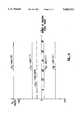
- FIG. 3outlines the key steps in the new algorithm used to erase with a minimum stress.
- FIG. 4shows the program/erase cycling endurance characteristics of the split channel Flash EEPROM device using intelligent algorithms for multistate programming and for reduced stress during erasing.
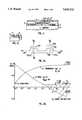
- a semiconductor substrate 11includes source region 13 and drain region 15, usually formed by ion implantation. Between the source and drain is a channel region 17. Over a portion of the channel region designated as L1 is a floating gate 19, separated from the substrate by a thin layer of gate oxide 21. Over a portion of the channel region designated as L2 is formed a control gate 23, separated from the substrate 11 by a thin gate oxide layer 25. The control gate 23 is also electrically isolated from the floating gate 19 by an oxide layer 27.
- the desired charge levelis programmed by applying an appropriate combination of voltages to the source, drain, substrate and control gate, for a designated period of time, in order to cause electrons to move from the substrate 11 to the floating gate 19.
- the floating gateis confined to its one memory cell and is electrically isolated from all other parts of the structure.
- the split-channelhas the effect of providing two field-effect-transistors in series, one with the floating gate 19 and the control gate 23 controlling conduction of its channel and the other with the control gate 23 alone controlling conduction of its channel.
- the generic split-channel EPROM or EEPROM structure of FIG. 1becomes a Flash EEPROM device when an erase gate 31 (FIG. 1a) is added.
- the erase gateis a separate electrode positioned near a portion of the floating gate 27 and separated from it by a tunnel dielectric 33.
- a single erase gateextends to a large number of memory cells, if not the entire array, so that they may be erased all at once.
- Flash EEPROM cellsthe source or drain diffusions underneath the floating gate are used also as the erase electrode, while in other cells the erase electrode is implemented either in the same conductive layer as the control gate or in a separate conductive layer.
- the split channel Flash EEPROM devicecan be viewed as a composite transistor consisting of two transistors T1 and T2 in series--FIG. 2a.
- Transistor T1is a floating gate transistor of effective channel length L1 and having a variable threshold voltage V T1 .
- Transistor T2has a fixed (enhancement) threshold voltage V T2 and an effective channel length L2.
- the EPROM programming characteristics of the composite transistorare shown in curve (a) of FIG. 2b.
- V CGno programming can occur if either one of V CG or V D is at 0 V.
- Prior art devicesemploy a so called "intelligent programming" algorithm whereby programming pulses are applied, each of typically 100 microseconds to 1 millisecond duration, followed by a sensing (read) operation. Pulses are applied until the device is sensed to be fully in the off state, and then one to three more programming pulses are applied to ensure solid programmability.
- This inventionproposes for the first time a scheme to take advantage of the full memory window. This is done by using the wider memory window to store more than two binary states and therefore more than a single bit per cell. For example, it is possible to store 4, rather than 2 states per cell, with these states having the following threshold voltage:
- the conduction current I DS of the composite transistor for all 4 statesis shown as a function of V CG in FIG. 2c.
- a current sensing amplifieris capable of easily distinguishing between these four conduction states.
- the maximum number of states which is realistically feasibleis influenced by the noise sensitivity of the sense amplifier as well as by any charge loss which can be expected over time at elevated temperatures. Eight distinct conduction states are necessary for 3 bit storage per cell, and 16 distinct conduction states are required for 4 bit storage per cell.
- Multistate memory cellshave previously been proposed in conjunction with ROM (Read Only Memory) devices and DRAM (Dynamic Random Access Memory).
- ROMRead Only Memory
- DRAMDynamic Random Access Memory
- each storage transistorcan have one of several fixed conduction states by having different channel ion implant doses to establish more than two permanent threshold voltage states.
- Prior art multistate DRAM cellshave also been proposed where each cell in the array is physically identical to all other cells. However, the charge stored at the capacitor of each cell may be quantized, resulting in several distinct read signal levels.
- An example of such prior art multistate DRAM storageis described in IEEE Journal of Solid-State Circuits, February 1988, p. 27 in an article by M. Horiguchi et al. entitled "An Experimental Large-Capacity Semiconductor File Memory Using 16-Levels/Cell Storage".
- the programming algorithmallow programming of the device into any one of several conduction states.
- the devicebe erased to a voltage V T1 more negative than the "3" state (-3.0 V in this example).
- the deviceis programmed in a short programming pulse, typically one to ten microseconds in duration. Programming conditions are selected such that no single pulse can shift the device threshold by more than one half of the threshold voltage difference between two successive states.
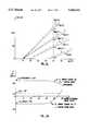
- FIG. 2eAn example of one such circuit is shown in FIG. 2e.
- an array of memory cellshas decoded word lines and decoded bit lines connected to the control gates and drains respectively of rows and columns of cells.
- FIG. 2fshows voltages V PWL and V PBL during operation of the circuit of FIG. 2e.
- Each bit lineis normally precharged to a voltage of between 1.0 V and 2.0 V during the time between read, program or erase.
- four sense amplifierseach with its own distinct current reference levels IREF,0, IREF,1, IREF,2, and IREF,3 are attached to each decoded output of the bit line.
- the current through the Flash EEPROM transistoris compared simultaneously (i.e., in parallel) with these four reference levels (this operation can also be performed in four consecutive read cycles using a single sense amplifier with a different reference applied at each cycle, if the attendant additional time required for reading is not a concern).
- the data outputis provided from the four sense amplifiers through four Di buffers (DO, D1, D2 and D3).
- the four data inputs Ii(I0, I1, I2 and I3) are presented to a comparator circuit which also has presented to it the four sense amp outputs for the accessed cell. If Di match Ii, then the cell is in the correct state and no programming is required. If however all four Di do not match all four Ii, then the comparator output activates a programming control circuit. This circuit in turn controls the bit line (VPBL) and word line (VPWL) programming pulse generators. A single short programming pulse is applied to both the selected word line and the selected bit line. This is followed by a second read cycle to determine if a match between Di and Ii has been established. This sequence is repeated through multiple programming/reading pulses and is stopped only when a match is established (or earlier if no match has been established but after a preset maximum number of pulses has been reached).
- each cellis programmed into any one of the four conduction states in direct correlation with the reference conduction states I REF , i.
- the same sense amplifiers used during programming/reading pulsingare also used during sensing (i.e., during normal reading).
- Thisallows excellent tracking between the reference levels (dashed lines in FIG. 2c) and the programmed conduction levels (solid lines in FIG. 2c), across large memory arrays and also for a very wide range of operating temperatures.
- the deviceexperiences the minimum amount of endurance-related stress possible.
- circuits of FIG. 2ecan be used also with binary storage, or with storage of more than four states per cell.
- circuits other than the one shown in FIG. 2eare also possible.
- voltage level sensingrather than conduction level sensing can be employed.
- states “3" and “2"are the result of net positive charge (holes) on the floating gate while states “1" and “0” are the result of net negative charge (electrons) on the floating gate.
- states “3" and “2”are the result of net positive charge (holes) on the floating gate while states “1" and “0” are the result of net negative charge (electrons) on the floating gate.
- This conditionis readily met for stored electrons in this as well as all prior art EPROM and Flash EEPROM devices. From device physics considerations, retention of holes trapped on the floating gate should be significantly superior to the retention of trapped electrons. This is so because trapped holes can only be neutralized by the injection of electrons onto the floating gate. So long as the conditions for such injection do not exist, it is
- Flash EEPROM devicesThe endurance of Flash EEPROM devices is their ability to withstand a given number of program/erase cycles.
- the physical phenomenon limiting the endurance of prior art Flash EEPROM devicesis trapping of electrons in the active dielectric films of the device.
- the dielectric used during hot electron channel injectiontraps part of the injected electrons.
- the tunnel erase dielectriclikewise traps some of the tunneled electrons. The trapped electrons oppose the applied electric field in subsequent write/erase cycles thereby causing a reduction in the threshold voltage shift of V tx . This can be seen in a gradual closure (FIG. 2d) in the voltage "window" between the "0" and "1" states.
- the window closurecan become sufficiently severe to cause the sensing circuitry to malfunction. If cycling is continued, the device eventually experiences catastrophic failure due to a ruptured dielectric. This typically occurs at between 1 ⁇ 10 6 and 1 ⁇ 10 7 cycles, and is known as the intrinsic breakdown of the device. In memory arrays of prior art devices the window closure is what limits the practical endurance to approximately 1 ⁇ 10 4 cycles. At a given erase voltage, V ERASE , the time required to adequately erase the device can stretch out from 100 milliseconds initially (i.e. in a virgin device) to 10 seconds in a device which has been cycled through 1 ⁇ 10 4 cycles.
- Flash EEPROM devicesspecified to withstand 1 ⁇ 10 4 cycles must specify a sufficiently long erase pulse duration to allow proper erase after 1 ⁇ 10 4 cycles. However, this also results in virgin devices being overerased and therefore being unnecessarily overstressed.
- FIG. 3outlines the main steps in the sequence of the new erase algorithm. Assume that a block array of mxn memory cells is to be fully erased (Flash erase) to state "3"(highest conductivity and lowest V T1 state). Certain parameters are established in conjunction with the erase algorithm. They are listed in FIG. 3: V 1 is the erase voltage of the first erase pulse. V 1 is lower by perhaps 5 volts from the erase voltage required to erase a virgin device to state "3" in a one second erase pulse. t is chosen to be approximately 1/10th of the time required to fully erase a virgin device to state "3". Typically, V 1 may be between 10 and 20 volts while t may be between 10 and 100 milliseconds.
- a cellis considered to be fully erased when its read conductance is greater than I "3" .
- the number S (an experience number) of complete erase cyclings experienced by each blockis an important information at the system level. If S is known for each block then a block can be replaced automatically with a new redundant block once S reaches 1 ⁇ 10 6 (or any other set number) of program/erase cycles. S is set at zero initially, and is incremented by one for each complete block erase multiple pulse cycle.
- the value of S at any one timecan be stored by using for example twenty bits (2 20 equals approximately 1 ⁇ 10 6 ) in each block. That way each block carries its own endurance history. Alternatively the S value can be stored off chip as part of the system.
- Nis greater than x (array not adequately erased) a second erase pulse is applied of magnitude greater by ⁇ V than the magnitude of the first pulse, with the same pulse duration, t. Read diagonal cells, count N.
- the final erase pulseis applied to assure that the array is solidly and fully erased.
- the magnitude of V ERASEcan be the same as in the previous pulse br higher by another increment ⁇ V.
- the durationcan be between 1t and 5t.
- Nis greater than X, then address locations of the N unerased cells are generated, possibly for substitution with redundant good bits at the system level. If N is significantly larger than X (for example, if N exceeds a second number of cells such that N represents perhaps 5% of the total number of cells), then a flag may be raised, to indicate to the user that the array may have reached its endurance limit.
- Sis incremented by one and the new S is stored for future reference. This step is optional.
- the new Scan be stored either by writing it into the newly erased block or off chip in a separate register file.
- the erase cycleis ended.
- the complete cycleis expected to be completed with between 10 to 20 erase pulses and to last a total of approximately one second.
- the total erase timeis significantly shorter than the fixed V ERASE pulse of the prior art. Virgins devices see the minimum pulse duration necessary to erase. Devices which have undergone more than 1 ⁇ 10 4 cycles require only several more ⁇ V voltage increments to overcome dielectric trapped charge, which only adds several hundred milliseconds to their total erase time.
- FIG. 4shows the four conduction states of the Flash EEPROM devices of this invention as a function of the number of program/erase cycles. Since all four states are always accomplished by programming or erasing to fixed reference conduction states, there is no window closure for any of these states at least until 1 ⁇ 10 6 cycles.
- a Flash EEPROM memory chipit is possible to implement efficiently the new erase algorithm by providing on chip (or alternatively on a separate controller chip) a voltage multiplier to provide the necessary voltage V1 and voltage increments ⁇ V to n ⁇ V, timing circuitry to time the erase and sense pulse duration, counting circuitry to count N and compare it with the stored value for X, registers to store address locations of bad bits, and control and sequencing circuitry, including the instruction set to execute the erase sequence outlined above.
Landscapes
- Engineering & Computer Science (AREA)
- Computer Hardware Design (AREA)
- Microelectronics & Electronic Packaging (AREA)
- Read Only Memory (AREA)
Abstract
Description
This application in a continuation of application Ser. No. 08/389,295 filed Feb. 16, 1995, now U.S. Pat. No. 5,583,812, which is a continuation of Ser. No. 08/116,867, filed Sep. 3, 1993, now U.S. Pat. No. 5,434,825, which is a division of application Ser. No. 07/563,287, filed Aug. 6, 1990, now U.S. Pat. No. 5,268,870, which in turn is a division of application Ser. No. 07/380,854, filed Jul. 17, 1989, now U.S. Pat. No. 5,043,940, which in turn is a division of application Ser. No. 07/204,175, filed Jun. 8, 1988, now U.S. Pat. No. 5,095,344.
This invention relates generally to semiconductor electrically programmable read only memories (EPROM) and electrically erasable programmable read only memories (EEPROM), and specifically to techniques for using them.
An electrically programmable read only memory (EPROM) utilizes a floating (unconnected) conductive gate, in a field effect transistor structure, positioned over but insulated from a channel region in a semiconductor substrate, between source and drain regions. A control gate is then provided over the floating gate, but also insulated therefrom. The threshold voltage characteristic of the transistor is controlled by the amount of charge that is retained on the floating gate. That is, the minimum amount of voltage (threshold) that must be applied to the control gate before the transistor is turned "on" to permit conduction between its source and drain regions is controlled by the level of charge on the floating gate. A transistor is programmed to one of two states by accelerating electrons from the substrate channel region, through a thin gate dielectric and onto the floating gate.
The memory cell transistor's state is read by placing an operating voltage across its source and drain and on its control gate, and then detecting the level of current flowing between the source and drain as to whether the device is programmed to be "on" or "off" at the control gate voltage selected. A specific, single cell in a two-dimensional array of EPROM cells is addressed for reading by application of a source-drain voltage to source and drain lines in a column containing the cell being addressed, and application of a control gate voltage to the control gates in a row containing the cell being addressed.
One example of such a memory cell is a triple polysilicon, split channel electrically erasable and programmable read only memory (EEPROM). It is termed a "split channel" device since the floating and control gates extend over adjacent portions of the channel. This results in a transistor structure that operates as two transistors in series, one having a varying threshold in response to the charge level on the floating gate, and another that is unaffected by the floating gate charge but rather which operates in response to the voltage on the control gate as in any normal field effect transistor.
Such a memory cell is termed a "triple polysilicon" cell because it contains three conductive layers of polysilicon materials. In addition to the floating and control gates, an erase gate is included. The erase gate passes through each memory cell transistor closely adjacent to a surface of the floating gate but insulated therefrom by a thin tunnel dielectric. Charge is then removed from the floating gate of a cell to the erase gate, when appropriate voltages are applied to all the transistor elements. An array of EEPROM cells are generally referred to as a Flash EEPROM array if an entire array of cells, or a significant group of cells, is erased simultaneously (i.e., in a flash).
EEPROM's have been found to have a limited effective life. The number of cycles of programming and erasing that such a device can endure before becoming degraded is finite. After a number of such cycles in excess of 10,000, depending upon its specific structure, its programmability can be reduced. Often, by the time the device has been put through such a cycle for over 100,000 times, it can no longer be programmed or erased properly. This is believed to be the result of electrons being trapped in the dielectric each time charge is transferred to or away from the floating gate by programming or erasing, respectively.
It is a primary object of the present invention to provide an EEPROM array with increased storage capacity and life.
Further, it is an object of the present invention to provide techniques for increasing the number of program/erase cycles that an EEPROM can endure.
Another object of the present invention is to provide techniques for increasing the amount of information that can be stored in a given size EPROM or EEPROM array.
It is yet another object of the present invention to provide EEPROM semiconductor chips that are useful for solid state memory to replace magnetic disk storage devices.
These and additional objects are accomplished by the various aspects of the present invention, wherein, briefly and generally, each EPROM or EEprom memory cell is caused to store more than one bit of data by partitioning its programmed charge into three or more ranges. Each cell is then programmed into one of these ranges. If four ranges are used, two bits of data can be stored in a single cell. If eight ranges are designated, three bits can be stored, and so on.
An intelligent programming and sensing technique is provided which permits the practical implementation of such multiple state storage. Further, an intelligent erase algorithm is provided which results in a significant reduction in the electrical stress experienced by the erase tunnel dielectric and results in much higher endurance to program/erase cycling and a resulting increased life of the memory.
Additional objects, features and advantages of the present invention will be understood from the following description of its preferred embodiments, which description should be taken in conjunction with the accompanying drawings.
FIG. 1a is a cross-sectional view of a Flash EEPROM cell.
FIG. 1 is a cross section of an example split channel EPROM or EEprom.
FIG. 2a is a schematic representation of the composite transistor forming a split channel EPROM device.
FIG. 2b shows the programming and erase characteristics of a split channel Flash EEPROM device.
FIG. 2c shows the four conduction states of a split channel Flash EEPROM device in accordance with this invention.
FIG. 2d shows the program/erase cycling endurance characteristics of prior art Flash EEPROM devices.
FIG. 2e and 2f show a circuit schematic and programming/read voltage pulses required to implement multistate storage.
FIG. 3 outlines the key steps in the new algorithm used to erase with a minimum stress.
FIG. 4 shows the program/erase cycling endurance characteristics of the split channel Flash EEPROM device using intelligent algorithms for multistate programming and for reduced stress during erasing.
Referring initially to FIG. 1, the structure of a split-channel EPROM or EEPROM cell is described that is suitable for use in the improved memory array and operation of the present invention. A semiconductor substrate 11 includessource region 13 and drainregion 15, usually formed by ion implantation. Between the source and drain is a channel region 17. Over a portion of the channel region designated as L1 is a floatinggate 19, separated from the substrate by a thin layer ofgate oxide 21. Over a portion of the channel region designated as L2 is formed acontrol gate 23, separated from the substrate 11 by a thingate oxide layer 25. Thecontrol gate 23 is also electrically isolated from the floatinggate 19 by anoxide layer 27.
It is the amount of electrical charge on the floatinggate 19 that is programmed in accordance with the state desired to be stored in the cell. If the charge level is above some set threshold, the cell is considered to be in one state. If below that threshold, it is designated to be in its other state. The desired charge level is programmed by applying an appropriate combination of voltages to the source, drain, substrate and control gate, for a designated period of time, in order to cause electrons to move from the substrate 11 to the floatinggate 19.
The floating gate is confined to its one memory cell and is electrically isolated from all other parts of the structure. Thecontrol gate 23, on the other hand, extends across a large number of cells sharing a common word line. As described hereinafter, the split-channel has the effect of providing two field-effect-transistors in series, one with the floatinggate 19 and thecontrol gate 23 controlling conduction of its channel and the other with thecontrol gate 23 alone controlling conduction of its channel.
The generic split-channel EPROM or EEPROM structure of FIG. 1 becomes a Flash EEPROM device when an erase gate 31 (FIG. 1a) is added. The erase gate is a separate electrode positioned near a portion of the floatinggate 27 and separated from it by atunnel dielectric 33. When the proper voltages are applied to the source, drain, substrate, control gate and erase gate, the amount of charge on the floating gate is reduced. A single erase gate extends to a large number of memory cells, if not the entire array, so that they may be erased all at once. In some prior art Flash EEPROM cells the source or drain diffusions underneath the floating gate are used also as the erase electrode, while in other cells the erase electrode is implemented either in the same conductive layer as the control gate or in a separate conductive layer.
The split channel Flash EEPROM device can be viewed as a composite transistor consisting of two transistors T1 and T2 in series--FIG. 2a. Transistor T1 is a floating gate transistor of effective channel length L1 and having a variable threshold voltage VT1. Transistor T2 has a fixed (enhancement) threshold voltage VT2 and an effective channel length L2. The EPROM programming characteristics of the composite transistor are shown in curve (a) of FIG. 2b. The programmed threshold voltage Vtx is plotted as a function of the time t during which the programming conditions are applied. These programming conditions typically are VCG =12 V, VD =9 V, Vs =VBB =0 V, where VBB is the substrate voltage. No programming can occur if either one of VCG or VD is at 0 V. A virgin (unprogrammed, unerased) device has VT1 =+1.5 V and VT2 =+1.0 V. After programming for approximately 100 microseconds the device reaches a threshold voltage Vtx ≧+6.0 volts. This represents the off ("0") state because the composite device does not conduct at VCG =+5.0 V. Prior art devices employ a so called "intelligent programming" algorithm whereby programming pulses are applied, each of typically 100 microseconds to 1 millisecond duration, followed by a sensing (read) operation. Pulses are applied until the device is sensed to be fully in the off state, and then one to three more programming pulses are applied to ensure solid programmability.
Prior art split channel Flash EEPROM devices erase with a single pulse of sufficient voltage VERASE and sufficient duration to ensure that VT1 is erased to a voltage below VT2 (curve (b) in FIG. 2b). Although the floating gate transistor may continue to erase into depletion mode operation (line (c) in FIG. 2b), the presence of the series T2 transistor obscures this depletion threshold voltage. Therefore the erased on ("1") state is represented by the threshold voltage Vtx =VT2 =+1.0 V. The memory storage "window" is given by ΔV=Vtx ("0")-Vtx ("1")=6.0-1.0 =5.0 V. However, the true memory storage window should be represented by the full swing of Vtx for transistor T1. For example, if T1 is erased into depletion threshold voltage VT1 =-3.0 V, then the true window should be given by--ΔV=6.0-(-3.0)=9.0 V. None of the prior art Flash EEPROM devices take advantage of the true memory window. In fact they ignore altogether the region of device operation (hatched region D in FIG. 2b) where VT1 is more negative than VT2.
This invention proposes for the first time a scheme to take advantage of the full memory window. This is done by using the wider memory window to store more than two binary states and therefore more than a single bit per cell. For example, it is possible to store 4, rather than 2 states per cell, with these states having the following threshold voltage:
______________________________________ State "3": V.sub.T1 = -3.0 V, V.sub.T2 = +1.0 V (highest conduction) = 1, 1. State "2": V.sub.T1 = -0.5 V, V.sub.T2 = +1.0 V (intermediate conduction) = 1, 0. State "1": V.sub.T1 = +2.0 V, V.sub.T2 = +1.0 V (lower conduction) = 0, 1. State "0": V.sub.T1 = +4.5 V, V.sub.T2 = +1.0 V (no conduction) = 0, 0. ______________________________________
To sense any one of these four states, the control gate is raised to VCG =+5.0 V and the source-drain current IDS is sensed through the composite device. Since VT2 =+1.0 V for all four threshold states transistor T2 behaves simply as a series resistor. The conduction current IDS of the composite transistor for all 4 states is shown as a function of VCG in FIG. 2c. A current sensing amplifier is capable of easily distinguishing between these four conduction states. The maximum number of states which is realistically feasible is influenced by the noise sensitivity of the sense amplifier as well as by any charge loss which can be expected over time at elevated temperatures. Eight distinct conduction states are necessary for 3 bit storage per cell, and 16 distinct conduction states are required for 4 bit storage per cell.
Multistate memory cells have previously been proposed in conjunction with ROM (Read Only Memory) devices and DRAM (Dynamic Random Access Memory). In ROM, each storage transistor can have one of several fixed conduction states by having different channel ion implant doses to establish more than two permanent threshold voltage states. Prior art multistate DRAM cells have also been proposed where each cell in the array is physically identical to all other cells. However, the charge stored at the capacitor of each cell may be quantized, resulting in several distinct read signal levels. An example of such prior art multistate DRAM storage is described in IEEE Journal of Solid-State Circuits, February 1988, p. 27 in an article by M. Horiguchi et al. entitled "An Experimental Large-Capacity Semiconductor File Memory Using 16-Levels/Cell Storage". A second example of prior art multistate DRAM is provided in IEEE Custom Integrated Circuits Conference, May 1988, p. 4.4.1 in an article entitled "An Experimental 2-Bit/Cell Storage DRAM for Macrocell or Memory-on-Logic Applications" by T. Furuyama et al.
To take full advantage of multistate storage in EPROMs it is necessary that the programming algorithm allow programming of the device into any one of several conduction states. First it is required that the device be erased to a voltage VT1 more negative than the "3" state (-3.0 V in this example). Then the device is programmed in a short programming pulse, typically one to ten microseconds in duration. Programming conditions are selected such that no single pulse can shift the device threshold by more than one half of the threshold voltage difference between two successive states. The device is then sensed by comparing its conduction current IDS with that of a reference current source IREF, i (i=0,1,2,3) corresponding to the desired conduction state (four distinct reference levels must be provided corresponding to the four states). Programming pulses are continued until the sensed current (solid lines in FIG. 2c) drops slightly below the reference current corresponding to the desired one of four states (dashed lines in FIG. 2c). To better illustrate this point, assume that each programming pulse raises Vtx linearly by 200 millivolts, and assume further that the device was first erased to VT1 =-3.2 V. Then the number of programming/sensing pulses required is:
______________________________________ For state "3" (V.sub.T1 = -3.0 V) No. of pulses = (3.2-3.0)/.2 = 1 For state "2" (V.sub.T1 = -0.5 V) No. of pulses = (3.2-0.5)/.2 = 14 For state "1" (V.sub.T1 = +2.0 V) No. of pulses = (3.2-(-2.0))/.2 = 26 and for state "0" (V.sub.T1 = +4.5 V) No. of pulses = (3.2-(-4.5))/.2 = 39. ______________________________________
In actual fact shifts in Vtx are not linear in time, as shown in FIG. 2b (curve (a)), therefore requiring more pulses than indicated for states "1" and "0". If 2 microseconds is the programming pulse width and 0.1 microseconds is the time required for sensing, then the maximum time required to program the device into any of the 4 states is approximately 39×2+39×0.1=81.9 microseconds. This is less than the time required by "intelligent programming algorithms" of prior art devices. In fact, with the new programming algorithm only carefully metered packets of electrons are injected during programming. A further benefit of this approach is that the sensing during reading is the same sensing as that during programming/sensing, and the same reference current sources are used in both programming and reading operations. That means that each and every memory cell in the array is read relative to the same reference level as used during program/sense. This provides excellent tracking even in very large memory arrays.
Large memory systems typically incorporate error detection and correction schemes which can tolerate a small number of hard failures i.e. bad Flash EEPROM cells. For this reason the programming/sensing cycling algorithm can be automatically halted after a certain maximum number of programming cycles has been applied even if the cell being programmed has not reached the desired threshold voltage state, indicating a faulty memory cell.
There are several ways to implement the multistate storage concept in conjunction with an array of Flash EEPROM transistors. An example of one such circuit is shown in FIG. 2e. In this circuit an array of memory cells has decoded word lines and decoded bit lines connected to the control gates and drains respectively of rows and columns of cells. FIG. 2f shows voltages VPWL and VPBL during operation of the circuit of FIG. 2e. Each bit line is normally precharged to a voltage of between 1.0 V and 2.0 V during the time between read, program or erase. For a four state storage, four sense amplifiers, each with its own distinct current reference levels IREF,0, IREF,1, IREF,2, and IREF,3 are attached to each decoded output of the bit line. During read, the current through the Flash EEPROM transistor is compared simultaneously (i.e., in parallel) with these four reference levels (this operation can also be performed in four consecutive read cycles using a single sense amplifier with a different reference applied at each cycle, if the attendant additional time required for reading is not a concern). The data output is provided from the four sense amplifiers through four Di buffers (DO, D1, D2 and D3).
During programming, the four data inputs Ii (I0, I1, I2 and I3) are presented to a comparator circuit which also has presented to it the four sense amp outputs for the accessed cell. If Di match Ii, then the cell is in the correct state and no programming is required. If however all four Di do not match all four Ii, then the comparator output activates a programming control circuit. This circuit in turn controls the bit line (VPBL) and word line (VPWL) programming pulse generators. A single short programming pulse is applied to both the selected word line and the selected bit line. This is followed by a second read cycle to determine if a match between Di and Ii has been established. This sequence is repeated through multiple programming/reading pulses and is stopped only when a match is established (or earlier if no match has been established but after a preset maximum number of pulses has been reached).
The result of such multistate programming algorithm is that each cell is programmed into any one of the four conduction states in direct correlation with the reference conduction states IREF, i. In fact, the same sense amplifiers used during programming/reading pulsing are also used during sensing (i.e., during normal reading). This allows excellent tracking between the reference levels (dashed lines in FIG. 2c) and the programmed conduction levels (solid lines in FIG. 2c), across large memory arrays and also for a very wide range of operating temperatures. Furthermore, because only a carefully metered number of electrons is introduced onto the floating gate during programming or removed during erasing, the device experiences the minimum amount of endurance-related stress possible.
In actual fact, although four reference levels and four sense amplifiers are used to program the cell into one of four distinct conduction states, only three sense amplifiers and three reference levels are required to sense the correct one of four stored states. For example, in FIG. 2c, IREF ("2")can differentiate correctly between conduction states "3" and "2", IREFF ("1") can differentiate correctly between conduction states "2" and "1", and IREF ("0")can differentiate correctly between conduction states "1" and "0". In a practical implementation of the circuit of FIG. 2e the reference levels IREF, i (i=0,1,2) may be somewhat shifted by a fixed amount during sensing to place them closer to the midpoint between the corresponding lower and higher conduction states of the cell being sensed.
Note that the same principle employed in the circuit of FIG. 2e can be used also with binary storage, or with storage of more than four states per cell. Of course, circuits other than the one shown in FIG. 2e are also possible. For example, voltage level sensing rather than conduction level sensing can be employed.
In the example above,states "3" and "2" are the result of net positive charge (holes) on the floating gate while states "1" and "0" are the result of net negative charge (electrons) on the floating gate. To properly sense the correct conduction state during the lifetime of the device (which may be specified as 10 years at 125 degrees centigrade) it is necessary for this charge not to leak off the floating gate by more than the equivalent of approximately 200 millivolts shift in VT1. This condition is readily met for stored electrons in this as well as all prior art EPROM and Flash EEPROM devices. From device physics considerations, retention of holes trapped on the floating gate should be significantly superior to the retention of trapped electrons. This is so because trapped holes can only be neutralized by the injection of electrons onto the floating gate. So long as the conditions for such injection do not exist, it is almost impossible for the holes to overcome the potential barrier of approximately 5.0 electron volts at the silicon--silicon dioxide interface (compared to a 3.1 electron volt potential barrier for trapped electrons).
Therefore, it is possible to improve the retention of this device by assigning more of the conduction states to states which involve trapped holes. For example, in the example above state "1" had VT1 =+2.0 V, which involved trapped electrons since VT1 for the virgin device was made to be VT1 =+1.5 V. If, however, VT1 of the virgin device is raised to a higher threshold voltage, say to VT1 =+3.0 V (e.g. by increasing the p-type doping concentration in the channel region 17 in FIG. 1), then the same state "1" with VT1 =+2.0 V will involve trapped holes, and will therefore better retain this value of VT1. Of course, it is also possible to set the reference levels so that most or all states will have values of VT1 which are lower than the VT1 of the virgin device.
The endurance of Flash EEPROM devices is their ability to withstand a given number of program/erase cycles. The physical phenomenon limiting the endurance of prior art Flash EEPROM devices is trapping of electrons in the active dielectric films of the device. During programming, the dielectric used during hot electron channel injection traps part of the injected electrons. During erasing, the tunnel erase dielectric likewise traps some of the tunneled electrons. The trapped electrons oppose the applied electric field in subsequent write/erase cycles thereby causing a reduction in the threshold voltage shift of Vtx. This can be seen in a gradual closure (FIG. 2d) in the voltage "window" between the "0" and "1" states. Beyond approximately 1×10⁴ program/erase cycles, the window closure can become sufficiently severe to cause the sensing circuitry to malfunction. If cycling is continued, the device eventually experiences catastrophic failure due to a ruptured dielectric. This typically occurs at between 1×10⁶ and 1×10⁷ cycles, and is known as the intrinsic breakdown of the device. In memory arrays of prior art devices the window closure is what limits the practical endurance to approximately 1×10⁴ cycles. At a given erase voltage, VERASE, the time required to adequately erase the device can stretch out from 100 milliseconds initially (i.e. in a virgin device) to 10 seconds in a device which has been cycled through 1×10⁴ cycles. In anticipation of such degradation, prior art Flash EEPROM devices specified to withstand 1×10⁴ cycles must specify a sufficiently long erase pulse duration to allow proper erase after 1×10⁴ cycles. However, this also results in virgin devices being overerased and therefore being unnecessarily overstressed.
A second problem with prior art devices is that during the erase pulse the tunnel dielectric may be exposed to an excessively high peak stress. This occurs in a device which has previously been programmed to state "0"(VT1 =+4.5 V or higher). This device has a large negative charge Q. When VERASE is applied, the tunnel dielectric is momentarily exposed to a peak electric field with contributions from VERASE as well as from Q. This peak field is eventually reduced when Q is reduced to zero as a consequence of the tunnel erase. Nevertheless, permanent and cumulative damage is inflicted through this erase procedure, which brings about premature device failure.
To overcome the two problems of overstress and window closure, a new erase algorithm is disclosed, which can also be applied equally well to any prior art Flash EEPROM device. Without such new erase algorithm, it would be difficult to have a multistate device since, from curve (b) in FIG. 2d, conduction states having VT1 more negative than VT2 may be eliminated after 1×10⁴ to 1×10⁵ write/erase cycles.
FIG. 3 outlines the main steps in the sequence of the new erase algorithm. Assume that a block array of mxn memory cells is to be fully erased (Flash erase) to state "3"(highest conductivity and lowest VT1 state). Certain parameters are established in conjunction with the erase algorithm. They are listed in FIG. 3: V1 is the erase voltage of the first erase pulse. V1 is lower by perhaps 5 volts from the erase voltage required to erase a virgin device to state "3" in a one second erase pulse. t is chosen to be approximately 1/10th of the time required to fully erase a virgin device to state "3". Typically, V1 may be between 10 and 20 volts while t may be between 10 and 100 milliseconds. The algorithm assumes that a certain small number, X, of bad bits can be tolerated by the system (through for example error detection and correction schemes implemented at the system level. If no error detection and correction is implemented then X=0). These would be bits which may have a shorted or leaky tunnel dielectric which prevents them from being erased even after a very long erase pulse. To avoid excessive erasing the total number of erase pulses in a complete block erase cycling can be limited to a preset number, nmax. ΔV is the voltage by which each successive erase pulse is incremented. Typically, ΔV is in the range between 0.25 V and 1.0 V. For example, if V1 =15.0 V and ΔV=l.0 V, then the seventh erase pulse will be of magnitude VERASE =21.0 V and duration t. A cell is considered to be fully erased when its read conductance is greater than I"3". The number S (an experience number) of complete erase cyclings experienced by each block is an important information at the system level. If S is known for each block then a block can be replaced automatically with a new redundant block once S reaches 1×10⁶ (or any other set number) of program/erase cycles. S is set at zero initially, and is incremented by one for each complete block erase multiple pulse cycle. The value of S at any one time can be stored by using for example twenty bits (220 equals approximately 1×10⁶) in each block. That way each block carries its own endurance history. Alternatively the S value can be stored off chip as part of the system.
The sequence for a complete erase cycle of the new algorithm is as follows (see FIG. 3):
1. Read S. This value can be stored in a register file. (This step can be omitted if S is not expected to approach the endurance limit during the operating lifetime of the device).
1a. Apply a first erase pulse with VERASE =V1 +n ΔV, n=0, pulse duration =t. This pulse (and the next few successive pulses) is insufficient to fully erase all memory cells, but it serves to reduce the charge Q on programmed cells at a relatively low erase field stress, i.e., it is equivalent to a "conditioning" pulse.
1b. Read a sparse pattern or selected number of cells in the array. A diagonal read pattern for example will read substantially less than all (m×n) cells required for a complete read, and will have at least one cell from each row and one cell from each column in the array. The number N of cells not fully erased to state "3" is counted and compared with X.
1c. If N is greater than x (array not adequately erased) a second erase pulse is applied of magnitude greater by ΔV than the magnitude of the first pulse, with the same pulse duration, t. Read diagonal cells, count N.
This cycling of erase pulse/read/increment erase pulse is continued until either N≦X, the number n of erase pulses exceed nmax the threshold level of each of the addressed cells has reached an erased state, or a predetermined maximum voltage VERASE of the erase pulse has been reached. The first one of these two conditions to occur leads to a final erase pulse.
2a. The final erase pulse is applied to assure that the array is solidly and fully erased. The magnitude of VERASE can be the same as in the previous pulse br higher by another increment ΔV. The duration can be between 1t and 5t.
2b. 100% of the array is read. The number N of cells not fully erased is counted. If N is less than or equal to X, then the erase pulsing is completed at this point.
2c. If N is greater than X, then address locations of the N unerased cells are generated, possibly for substitution with redundant good bits at the system level. If N is significantly larger than X (for example, if N exceeds a second number of cells such that N represents perhaps 5% of the total number of cells), then a flag may be raised, to indicate to the user that the array may have reached its endurance limit.
2d. Erase pulsing is ended.
3a. S is incremented by one and the new S is stored for future reference. This step is optional. The new S can be stored either by writing it into the newly erased block or off chip in a separate register file.
3b. The erase cycle is ended. The complete cycle is expected to be completed with between 10 to 20 erase pulses and to last a total of approximately one second.
The new algorithm has the following advantages:
(a) No cell in the array experiences the peak electric field stress. By the time VERASE is incremented to a relatively high voltage any charge Q on the floating gates has already been removed in previous lower voltage erase pulses.
(b) The total erase time is significantly shorter than the fixed VERASE pulse of the prior art. Virgins devices see the minimum pulse duration necessary to erase. Devices which have undergone more than 1×10⁴ cycles require only several more ΔV voltage increments to overcome dielectric trapped charge, which only adds several hundred milliseconds to their total erase time.
(c) The window closure on the erase side (curve (b) in FIG. 2d) is avoided indefinitely (until the device experiences failure by a catastrophic breakdown) because VERASE is simply incremented until the device is erased properly to state "3". Thus, the new erase algorithm preserves the full memory window.
FIG. 4 shows the four conduction states of the Flash EEPROM devices of this invention as a function of the number of program/erase cycles. Since all four states are always accomplished by programming or erasing to fixed reference conduction states, there is no window closure for any of these states at least until 1×10⁶ cycles.
In a Flash EEPROM memory chip, it is possible to implement efficiently the new erase algorithm by providing on chip (or alternatively on a separate controller chip) a voltage multiplier to provide the necessary voltage V1 and voltage increments ΔV to nΔV, timing circuitry to time the erase and sense pulse duration, counting circuitry to count N and compare it with the stored value for X, registers to store address locations of bad bits, and control and sequencing circuitry, including the instruction set to execute the erase sequence outlined above.
While the embodiments of this invention that have been described are the preferred implementations, those skilled in the art will understand that variations thereof may also be possible. Therefore, the invention is entitled to protection within the full scope of the appended claims.
Claims (14)
1. For an array of electrically alterable memory cells divided into blocks of cells and having means for addressing individual cells within said blocks to read and alter their states, said memory cells individually including a field effect transistor with a floating gate and having a threshold voltage level that is a given level in the absence of net charge on said floating gate but which is variable in accordance with an amount of net charge carried by said floating gate, a method of operating the array, comprising:
establishing a plurality of effective threshold voltage levels in excess of two that correspond to a plurality of detectable programmed states of the individual cells in excess of two,
setting the effective threshold voltage level of at least one addressed cell within one of said blocks from a starting level to one of the plurality of threshold voltage levels by altering the amount of charge on the floating gate of said addressed cell until the effective threshold voltage of said addressed cell is substantially equal to one of said plurality of effective threshold voltage levels, whereby the state of said addressed cell is set to one of said plurality of programmed states, setting the effective threshold voltage level including the steps of:
applying a given voltage to said addressed cell for a predetermined time sufficient to move the effective threshold voltage level of the addressed cell from the starting level toward said one of the plurality of threshold voltage levels,
thereafter reading an electrical parameter of the addressed cell to determine whether the effective threshold voltage of the addressed cell has reached said one of the plurality of threshold voltage levels, and
repeating the voltage applying and reading steps until it is detected by the reading step that the effective threshold voltage of the addressed cell has been set to said one of the plurality of threshold voltage levels.
2. The method of claim 1, wherein the voltage applying step includes making said given voltage and said predetermined time such that the effective threshold voltage of the addressed cell is changed by less than one-half a difference between two adjacent of said plurality of effective threshold voltage levels.
3. The method of claim 1 wherein the step of reading includes electrically interrogating the addressed cell and simultaneously comparing a resulting level of an electrical parameter of the addressed cell with a number of reference levels of two or more.
4. The method of claim 1, which additionally comprises, prior to setting the effective threshold voltage level of at least one addressed cell within one of said blocks, of resetting the effective threshold voltage levels of cells within said at least one block to a preset level by the steps of:
applying a given voltage to the cells within said at least one block for a predetermined time sufficient to move the effective threshold voltage level of the cells within said at least one block toward said preset level,
thereafter reading said electrical parameter of the cells within said at least one block to determine whether the effective threshold voltages of the individual cells within said at least one block have reached said preset level, and
repeating the steps of applying voltage and reading the states of the cells within said at least one block until it is detected that the effective threshold voltage of the cells within said at least one block have been reset to said preset level.
5. The method of claim 4 wherein said preset level is made to be substantially equal to one of said plurality of effective threshold voltage levels that correspond to a plurality of detectable programmed states of the individual cells.
6. The method of claim 4 wherein the given voltage applied to the cells within said at least one block during resetting of their effective threshold voltage levels increases when the voltage applying and reading steps are repeated.
7. The method of claim 4 wherein the step of reading said electrical parameter of the cells within said at least one block includes electrically interrogating the cells within said at least one block and simultaneously comparing a resulting level of said electrical parameter of individual ones of the cells within said at least one block with a number of reference levels of two or more.
8. The method of any one of claims 1-7 wherein at least two of said plurality of effective threshold levels result from a net positive charge on the floating gate of the individual cells.
9. The method of any one of claims 1-7 wherein the given threshold level of the individual cells is established to be at least three volts.
10. The method of any one of claims 1-7 wherein the repeating of the voltage applying and reading steps during setting the effective threshold voltage level of said at least one addressed cell is terminated after a preset maximum number of repeats of the voltage applying and reading steps have occurred during setting without setting the effective threshold voltage levels of the addressed cell to said one of the plurality of threshold voltage levels.
11. The method of any one of claims 1-7 wherein the repeating of the voltage applying and reading steps during resetting the effective threshold voltage levels of cells within said at least one block is terminated after a preset maximum number of repeats of the voltage applying and reading steps have occurred during resetting without resetting the effective threshold voltage level of a certain number of the individual cells within said at least one block to said preset level.
12. The method of any one of claims 1-7 which additionally comprises, in response to said at least one addressed cell becoming defective, of substituting therefore a redundant good cell within the array.
13. The method of any one of claims 1-7 which additionally comprises, in response to said at least one block of cells becoming defective, of substituting therefore at least one redundant block of cells within the array.
14. The method of any one of claims 1-7 which additionally comprises accumulating a count of a total number of times that at least one block of cells has been reset.
Priority Applications (1)
| Application Number | Priority Date | Filing Date | Title |
|---|---|---|---|
| US08/650,116US5642312A (en) | 1988-06-08 | 1996-05-22 | Flash EEPROM system cell array with more than two storage states per memory cell |
Applications Claiming Priority (6)
| Application Number | Priority Date | Filing Date | Title |
|---|---|---|---|
| US07/204,175US5095344A (en) | 1988-06-08 | 1988-06-08 | Highly compact eprom and flash eeprom devices |
| US07/380,854US5043940A (en) | 1988-06-08 | 1989-07-17 | Flash EEPROM memory systems having multistate storage cells |
| US07/563,287US5268870A (en) | 1988-06-08 | 1990-08-06 | Flash EEPROM system and intelligent programming and erasing methods therefor |
| US08/116,867US5434825A (en) | 1988-06-08 | 1993-09-03 | Flash EEPROM system cell array with more than two storage states per memory cell |
| US08/389,295US5583812A (en) | 1988-06-08 | 1995-02-16 | Flash EEPROM system cell array with more than two storage states per memory cell |
| US08/650,116US5642312A (en) | 1988-06-08 | 1996-05-22 | Flash EEPROM system cell array with more than two storage states per memory cell |
Related Parent Applications (1)
| Application Number | Title | Priority Date | Filing Date |
|---|---|---|---|
| US08/389,295ContinuationUS5583812A (en) | 1988-06-08 | 1995-02-16 | Flash EEPROM system cell array with more than two storage states per memory cell |
Publications (1)
| Publication Number | Publication Date |
|---|---|
| US5642312Atrue US5642312A (en) | 1997-06-24 |
Family
ID=27394632
Family Applications (10)
| Application Number | Title | Priority Date | Filing Date |
|---|---|---|---|
| US07/563,287Expired - LifetimeUS5268870A (en) | 1988-06-08 | 1990-08-06 | Flash EEPROM system and intelligent programming and erasing methods therefor |
| US08/116,867Expired - LifetimeUS5434825A (en) | 1988-06-08 | 1993-09-03 | Flash EEPROM system cell array with more than two storage states per memory cell |
| US08/389,295Expired - LifetimeUS5583812A (en) | 1988-06-08 | 1995-02-16 | Flash EEPROM system cell array with more than two storage states per memory cell |
| US08/400,034Expired - LifetimeUS5544118A (en) | 1988-06-08 | 1995-03-07 | Flash EEPROM system cell array with defect management including an error correction scheme |
| US08/468,061Expired - LifetimeUS5568439A (en) | 1988-06-08 | 1995-06-06 | Flash EEPROM system which maintains individual memory block cycle counts |
| US08/650,116Expired - LifetimeUS5642312A (en) | 1988-06-08 | 1996-05-22 | Flash EEPROM system cell array with more than two storage states per memory cell |
| US08/652,725Expired - Fee RelatedUS5712819A (en) | 1988-06-08 | 1996-05-22 | Flash EEPROM system with storage of sector characteristic information within the sector |
| US08/991,650Expired - Fee RelatedUS5909390A (en) | 1988-06-08 | 1997-12-16 | Techniques of programming and erasing an array of multi-state flash EEPROM cells including comparing the states of the cells to desired values |
| US08/994,164Expired - Fee RelatedUS5835415A (en) | 1988-06-08 | 1997-12-29 | Flash EEPROM memory systems and methods of using them |
| US09/003,024Expired - Fee RelatedUS5862081A (en) | 1988-06-08 | 1998-01-05 | Multi-state flash EEPROM system with defect management including an error correction scheme |
Family Applications Before (5)
| Application Number | Title | Priority Date | Filing Date |
|---|---|---|---|
| US07/563,287Expired - LifetimeUS5268870A (en) | 1988-06-08 | 1990-08-06 | Flash EEPROM system and intelligent programming and erasing methods therefor |
| US08/116,867Expired - LifetimeUS5434825A (en) | 1988-06-08 | 1993-09-03 | Flash EEPROM system cell array with more than two storage states per memory cell |
| US08/389,295Expired - LifetimeUS5583812A (en) | 1988-06-08 | 1995-02-16 | Flash EEPROM system cell array with more than two storage states per memory cell |
| US08/400,034Expired - LifetimeUS5544118A (en) | 1988-06-08 | 1995-03-07 | Flash EEPROM system cell array with defect management including an error correction scheme |
| US08/468,061Expired - LifetimeUS5568439A (en) | 1988-06-08 | 1995-06-06 | Flash EEPROM system which maintains individual memory block cycle counts |
Family Applications After (4)
| Application Number | Title | Priority Date | Filing Date |
|---|---|---|---|
| US08/652,725Expired - Fee RelatedUS5712819A (en) | 1988-06-08 | 1996-05-22 | Flash EEPROM system with storage of sector characteristic information within the sector |
| US08/991,650Expired - Fee RelatedUS5909390A (en) | 1988-06-08 | 1997-12-16 | Techniques of programming and erasing an array of multi-state flash EEPROM cells including comparing the states of the cells to desired values |
| US08/994,164Expired - Fee RelatedUS5835415A (en) | 1988-06-08 | 1997-12-29 | Flash EEPROM memory systems and methods of using them |
| US09/003,024Expired - Fee RelatedUS5862081A (en) | 1988-06-08 | 1998-01-05 | Multi-state flash EEPROM system with defect management including an error correction scheme |
Country Status (1)
| Country | Link |
|---|---|
| US (10) | US5268870A (en) |
Cited By (87)
| Publication number | Priority date | Publication date | Assignee | Title |
|---|---|---|---|---|
| US5771346A (en)* | 1996-10-24 | 1998-06-23 | Micron Quantum Devices, Inc. | Apparatus and method for detecting over-programming condition in multistate memory device |
| US5835415A (en)* | 1988-06-08 | 1998-11-10 | Harari; Eliyahou | Flash EEPROM memory systems and methods of using them |
| WO1999014758A1 (en)* | 1997-09-16 | 1999-03-25 | Intel Corporation | Sense amplifier for flash memories |
| WO1999024988A1 (en)* | 1997-11-07 | 1999-05-20 | Silicon Storage Technology, Inc. | A sensing circuit for a floating gate memory device having multiple levels of storage in a cell |
| US5963480A (en)* | 1988-06-08 | 1999-10-05 | Harari; Eliyahou | Highly compact EPROM and flash EEPROM devices |
| US5970012A (en)* | 1996-09-30 | 1999-10-19 | Nec Corporation | Non-volatile semiconductor memory device having a memory cell capable of establishing multi-level information and data writing method thereof |
| US6002614A (en) | 1991-02-08 | 1999-12-14 | Btg International Inc. | Memory apparatus including programmable non-volatile multi-bit memory cell, and apparatus and method for demarcating memory states of the cell |
| US6028785A (en)* | 1998-06-29 | 2000-02-22 | Hyundai Electronics Industries Co., Inc. | Memory device for storing multi-data |
| US6031760A (en)* | 1997-07-29 | 2000-02-29 | Kabushiki Kaisha Toshiba | Semiconductor memory device and method of programming the same |
| US6034897A (en)* | 1999-04-01 | 2000-03-07 | Lexar Media, Inc. | Space management for managing high capacity nonvolatile memory |
| US6038166A (en)* | 1998-04-01 | 2000-03-14 | Invox Technology | High resolution multi-bit-per-cell memory |
| US6075725A (en)* | 1997-12-29 | 2000-06-13 | Samsung Electronics Co., Ltd. | Multilevel memory devices having memory cell referenced word line voltage generators with predetermined offsets |
| US6104640A (en)* | 1991-02-08 | 2000-08-15 | Btg International Inc. | Electrically alterable non-violatile memory with N-bits per cell |
| US6122195A (en)* | 1997-03-31 | 2000-09-19 | Lexar Media, Inc. | Method and apparatus for decreasing block write operation times performed on nonvolatile memory |
| US6128695A (en)* | 1995-07-31 | 2000-10-03 | Lexar Media, Inc. | Identification and verification of a sector within a block of mass storage flash memory |
| US6137726A (en)* | 1997-11-25 | 2000-10-24 | Samsung Electronics Co., Ltd. | Multi-level memory devices having memory cell referenced word line voltage generations |
| US6141249A (en)* | 1999-04-01 | 2000-10-31 | Lexar Media, Inc. | Organization of blocks within a nonvolatile memory unit to effectively decrease sector write operation time |
| US6163479A (en)* | 1996-10-24 | 2000-12-19 | Micron Technology, Inc. | Method for performing analog over-program and under-program detection for a multistate memory cell |
| US6175937B1 (en) | 1996-10-24 | 2001-01-16 | Micron Technology, Inc. | Apparatus and method for programming multistate memory device |
| US6202138B1 (en) | 1995-07-31 | 2001-03-13 | Lexar Media, Inc | Increasing the memory performance of flash memory devices by writing sectors simultaneously to multiple flash memory devices |
| US6262918B1 (en) | 1999-04-01 | 2001-07-17 | Lexar Media, Inc. | Space management for managing high capacity nonvolatile memory |
| US6353554B1 (en) | 1995-02-27 | 2002-03-05 | Btg International Inc. | Memory apparatus including programmable non-volatile multi-bit memory cell, and apparatus and method for demarcating memory states of the cell |
| US6374337B1 (en) | 1998-11-17 | 2002-04-16 | Lexar Media, Inc. | Data pipelining method and apparatus for memory control circuit |
| US6411546B1 (en) | 1997-03-31 | 2002-06-25 | Lexar Media, Inc. | Nonvolatile memory using flexible erasing methods and method and system for using same |
| US6466476B1 (en) | 2001-01-18 | 2002-10-15 | Multi Level Memory Technology | Data coding for multi-bit-per-cell memories having variable numbers of bits per memory cell |
| US6552932B1 (en) | 2001-09-21 | 2003-04-22 | Sandisk Corporation | Segmented metal bitlines |
| US20030079149A1 (en)* | 2001-09-28 | 2003-04-24 | Edwin Payne Robert | Power management system |
| US6560146B2 (en) | 2001-09-17 | 2003-05-06 | Sandisk Corporation | Dynamic column block selection |
| US6567307B1 (en) | 2000-07-21 | 2003-05-20 | Lexar Media, Inc. | Block management for mass storage |
| US6567302B2 (en) | 1998-12-29 | 2003-05-20 | Micron Technology, Inc. | Method and apparatus for programming multi-state cells in a memory device |
| US20030206449A1 (en)* | 1989-04-13 | 2003-11-06 | Eliyahou Harari | Flash EEprom system |
| US6662263B1 (en) | 2000-03-03 | 2003-12-09 | Multi Level Memory Technology | Sectorless flash memory architecture |
| US6728851B1 (en) | 1995-07-31 | 2004-04-27 | Lexar Media, Inc. | Increasing the memory performance of flash memory devices by writing sectors simultaneously to multiple flash memory devices |
| US6741502B1 (en) | 2001-09-17 | 2004-05-25 | Sandisk Corporation | Background operation for memory cells |
| US6757800B1 (en) | 1995-07-31 | 2004-06-29 | Lexar Media, Inc. | Increasing the memory performance of flash memory devices by writing sectors simultaneously to multiple flash memory devices |
| US20040190347A1 (en)* | 2001-09-17 | 2004-09-30 | Raul-Adrian Cernea | Dynamic column block selection |
| US6801979B1 (en) | 1995-07-31 | 2004-10-05 | Lexar Media, Inc. | Method and apparatus for memory control circuit |
| US6813678B1 (en) | 1998-01-22 | 2004-11-02 | Lexar Media, Inc. | Flash memory system |
| US20040240269A1 (en)* | 2001-09-17 | 2004-12-02 | Raul-Adrian Cernea | Latched programming of memory and method |
| US20040246798A1 (en)* | 1997-08-07 | 2004-12-09 | Guterman Daniel C. | Novel multi-state memory |
| US20050018527A1 (en)* | 2001-09-28 | 2005-01-27 | Gorobets Sergey Anatolievich | Non-volatile memory control |
| US6898662B2 (en) | 2001-09-28 | 2005-05-24 | Lexar Media, Inc. | Memory system sectors |
| US20050141387A1 (en)* | 2003-12-31 | 2005-06-30 | Raul-Adrian Cernea | Flexible and area efficient column redundancy for non-volatile memories |
| US6950918B1 (en) | 2002-01-18 | 2005-09-27 | Lexar Media, Inc. | File management of one-time-programmable nonvolatile memory devices |
| US6957295B1 (en) | 2002-01-18 | 2005-10-18 | Lexar Media, Inc. | File management of one-time-programmable nonvolatile memory devices |
| US20050265080A1 (en)* | 2004-05-27 | 2005-12-01 | Renesas Technology Corp. | Semiconductor nonvolatile memory device |
| US6978342B1 (en) | 1995-07-31 | 2005-12-20 | Lexar Media, Inc. | Moving sectors within a block of information in a flash memory mass storage architecture |
| US7000064B2 (en) | 2001-09-28 | 2006-02-14 | Lexar Media, Inc. | Data handling system |
| US20060140010A1 (en)* | 2004-12-29 | 2006-06-29 | Lorenzo Bedarida | Method and system for reducing soft-writing in a multi-level flash memory |
| US7102671B1 (en) | 2000-02-08 | 2006-09-05 | Lexar Media, Inc. | Enhanced compact flash memory card |
| US7167944B1 (en) | 2000-07-21 | 2007-01-23 | Lexar Media, Inc. | Block management for mass storage |
| US7185208B2 (en) | 2001-09-28 | 2007-02-27 | Lexar Media, Inc. | Data processing |
| US20070103977A1 (en)* | 2005-11-08 | 2007-05-10 | Conley Kevin M | Retargetable memory cell redundancy methods |
| US7231643B1 (en) | 2002-02-22 | 2007-06-12 | Lexar Media, Inc. | Image rescue system including direct communication between an application program and a device driver |
| US20070211539A1 (en)* | 2006-03-09 | 2007-09-13 | Powerchip Semiconductor Corp. | Method for resetting threshold voltage of non-volatile memory |
| US7275686B2 (en) | 2003-12-17 | 2007-10-02 | Lexar Media, Inc. | Electronic equipment point-of-sale activation to avoid theft |
| US20080001652A1 (en)* | 2006-05-22 | 2008-01-03 | Denso Corporation | Electronic circuit device |
| US20080002464A1 (en)* | 2004-12-09 | 2008-01-03 | Eduardo Maayan | Non-volatile memory device and method for reading cells |
| US7340581B2 (en) | 2001-09-28 | 2008-03-04 | Lexar Media, Inc. | Method of writing data to non-volatile memory |
| US7370166B1 (en) | 2004-04-30 | 2008-05-06 | Lexar Media, Inc. | Secure portable storage device |
| US7464306B1 (en) | 2004-08-27 | 2008-12-09 | Lexar Media, Inc. | Status of overall health of nonvolatile memory |
| US7523249B1 (en) | 1995-07-31 | 2009-04-21 | Lexar Media, Inc. | Direct logical block addressing flash memory mass storage architecture |
| US7594063B1 (en) | 2004-08-27 | 2009-09-22 | Lexar Media, Inc. | Storage capacity status |
| US7656710B1 (en) | 2005-07-14 | 2010-02-02 | Sau Ching Wong | Adaptive operations for nonvolatile memories |
| US7725628B1 (en) | 2004-04-20 | 2010-05-25 | Lexar Media, Inc. | Direct secondary device interface by a host |
| US20100309719A1 (en)* | 2009-06-05 | 2010-12-09 | Yan Li | Folding Data Stored in Binary Format Into Multi-State Format Within Non-Volatile Memory Devices |
| US20100309720A1 (en)* | 2009-06-05 | 2010-12-09 | Bo Liu | Structure and Method for Shuffling Data Within Non-Volatile Memory Devices |
| US20100329007A1 (en)* | 2009-06-24 | 2010-12-30 | Hardwell Chibvongodze | Pointer Based Column Selection Techniques in Non-Volatile Memories |
| US20110002169A1 (en)* | 2009-07-06 | 2011-01-06 | Yan Li | Bad Column Management with Bit Information in Non-Volatile Memory Systems |
| US7917709B2 (en) | 2001-09-28 | 2011-03-29 | Lexar Media, Inc. | Memory system for data storage and retrieval |
| US20110153913A1 (en)* | 2009-12-18 | 2011-06-23 | Jianmin Huang | Non-Volatile Memory with Multi-Gear Control Using On-Chip Folding of Data |
| US8144512B2 (en) | 2009-12-18 | 2012-03-27 | Sandisk Technologies Inc. | Data transfer flows for on-chip folding |
| US8171203B2 (en) | 1995-07-31 | 2012-05-01 | Micron Technology, Inc. | Faster write operations to nonvolatile memory using FSInfo sector manipulation |
| US20120257451A1 (en)* | 2006-08-21 | 2012-10-11 | Micron Technology, Inc. | Non-volatile memory with both single and multiple level cells |
| CN101325089B (en)* | 2007-06-14 | 2012-11-21 | 三星电子株式会社 | Nonvolatile memory device and methods of programming and reading the same |
| US8681548B2 (en) | 2012-05-03 | 2014-03-25 | Sandisk Technologies Inc. | Column redundancy circuitry for non-volatile memory |
| US8725935B2 (en) | 2009-12-18 | 2014-05-13 | Sandisk Technologies Inc. | Balanced performance for on-chip folding of non-volatile memories |
| US8842473B2 (en) | 2012-03-15 | 2014-09-23 | Sandisk Technologies Inc. | Techniques for accessing column selecting shift register with skipped entries in non-volatile memories |
| US8897080B2 (en) | 2012-09-28 | 2014-11-25 | Sandisk Technologies Inc. | Variable rate serial to parallel shift register |
| US9076506B2 (en) | 2012-09-28 | 2015-07-07 | Sandisk Technologies Inc. | Variable rate parallel to serial shift register |
| US9224502B1 (en) | 2015-01-14 | 2015-12-29 | Sandisk Technologies Inc. | Techniques for detection and treating memory hole to local interconnect marginality defects |
| US9269446B1 (en) | 2015-04-08 | 2016-02-23 | Sandisk Technologies Inc. | Methods to improve programming of slow cells |
| US9342446B2 (en) | 2011-03-29 | 2016-05-17 | SanDisk Technologies, Inc. | Non-volatile memory system allowing reverse eviction of data updates to non-volatile binary cache |
| US9490035B2 (en) | 2012-09-28 | 2016-11-08 | SanDisk Technologies, Inc. | Centralized variable rate serializer and deserializer for bad column management |
| US9564219B2 (en) | 2015-04-08 | 2017-02-07 | Sandisk Technologies Llc | Current based detection and recording of memory hole-interconnect spacing defects |
| US9934872B2 (en) | 2014-10-30 | 2018-04-03 | Sandisk Technologies Llc | Erase stress and delta erase loop count methods for various fail modes in non-volatile memory |
| US10032524B2 (en) | 2015-02-09 | 2018-07-24 | Sandisk Technologies Llc | Techniques for determining local interconnect defects |
Families Citing this family (352)
| Publication number | Priority date | Publication date | Assignee | Title |
|---|---|---|---|---|
| EP0935255A2 (en) | 1989-04-13 | 1999-08-11 | SanDisk Corporation | Flash EEPROM system |
| US7447069B1 (en) | 1989-04-13 | 2008-11-04 | Sandisk Corporation | Flash EEprom system |
| GB2251324B (en)* | 1990-12-31 | 1995-05-10 | Intel Corp | File structure for a non-volatile semiconductor memory |
| GB2251323B (en)* | 1990-12-31 | 1994-10-12 | Intel Corp | Disk emulation for a non-volatile semiconductor memory |
| JP2582487B2 (en)* | 1991-07-12 | 1997-02-19 | インターナショナル・ビジネス・マシーンズ・コーポレイション | External storage system using semiconductor memory and control method thereof |
| US5438573A (en)* | 1991-09-13 | 1995-08-01 | Sundisk Corporation | Flash EEPROM array data and header file structure |
| US6230233B1 (en)* | 1991-09-13 | 2001-05-08 | Sandisk Corporation | Wear leveling techniques for flash EEPROM systems |
| US5761127A (en)* | 1991-11-20 | 1998-06-02 | Fujitsu Limited | Flash-erasable semiconductor memory device having an improved reliability |
| US6347051B2 (en)* | 1991-11-26 | 2002-02-12 | Hitachi, Ltd. | Storage device employing a flash memory |
| TW261687B (en)* | 1991-11-26 | 1995-11-01 | Hitachi Seisakusyo Kk | |
| JP3080743B2 (en)* | 1991-12-27 | 2000-08-28 | 日本電気株式会社 | Nonvolatile semiconductor memory device |
| JP3178909B2 (en)* | 1992-01-10 | 2001-06-25 | 株式会社東芝 | Semiconductor memory device |
| US6256642B1 (en)* | 1992-01-29 | 2001-07-03 | Microsoft Corporation | Method and system for file system management using a flash-erasable, programmable, read-only memory |
| JP3485938B2 (en)* | 1992-03-31 | 2004-01-13 | 株式会社東芝 | Nonvolatile semiconductor memory device |
| JPH05324489A (en)* | 1992-05-15 | 1993-12-07 | Toshiba Corp | Storage device |
| US5657332A (en) | 1992-05-20 | 1997-08-12 | Sandisk Corporation | Soft errors handling in EEPROM devices |
| US6549974B2 (en) | 1992-06-22 | 2003-04-15 | Hitachi, Ltd. | Semiconductor storage apparatus including a controller for sending first and second write commands to different nonvolatile memories in a parallel or time overlapped manner |
| JP3328321B2 (en)* | 1992-06-22 | 2002-09-24 | 株式会社日立製作所 | Semiconductor storage device |
| JP2647312B2 (en)* | 1992-09-11 | 1997-08-27 | インターナショナル・ビジネス・マシーンズ・コーポレイション | Batch erase nonvolatile semiconductor memory device |
| US5740395A (en)* | 1992-10-30 | 1998-04-14 | Intel Corporation | Method and apparatus for cleaning up a solid state memory disk storing floating sector data |
| US5479633A (en)* | 1992-10-30 | 1995-12-26 | Intel Corporation | Method of controlling clean-up of a solid state memory disk storing floating sector data |
| US5369616A (en)* | 1992-10-30 | 1994-11-29 | Intel Corporation | Method for assuring that an erase process for a memory array has been properly completed |
| US5870520A (en)* | 1992-12-23 | 1999-02-09 | Packard Bell Nec | Flash disaster recovery ROM and utility to reprogram multiple ROMS |
| US5491809A (en)* | 1993-01-05 | 1996-02-13 | Texas Instruments Incorporated | Smart erase algorithm with secure scheme for flash EPROMs |
| US5581723A (en)* | 1993-02-19 | 1996-12-03 | Intel Corporation | Method and apparatus for retaining flash block structure data during erase operations in a flash EEPROM memory array |
| US6078520A (en)* | 1993-04-08 | 2000-06-20 | Hitachi, Ltd. | Flash memory control method and information processing system therewith |
| KR970008188B1 (en) | 1993-04-08 | 1997-05-21 | 가부시끼가이샤 히다찌세이사꾸쇼 | Flash memory control method and information processing device using the same |
| US5359558A (en)* | 1993-08-23 | 1994-10-25 | Advanced Micro Devices, Inc. | Flash eeprom array with improved high endurance |
| US7137011B1 (en)* | 1993-09-01 | 2006-11-14 | Sandisk Corporation | Removable mother/daughter peripheral card |
| US5887145A (en)* | 1993-09-01 | 1999-03-23 | Sandisk Corporation | Removable mother/daughter peripheral card |
| SG49632A1 (en)* | 1993-10-26 | 1998-06-15 | Intel Corp | Programmable code store circuitry for a nonvolatile semiconductor memory device |
| US5633823A (en)* | 1994-12-01 | 1997-05-27 | Micron Technology, Inc. | Method of narrowing flash memory device threshold voltage distribution |
| US5650965A (en)* | 1993-11-15 | 1997-07-22 | Micron Technology, Inc. | Method of narrowing flash memory device threshold voltage distribution |
| JP3999822B2 (en)* | 1993-12-28 | 2007-10-31 | 株式会社東芝 | Storage system |
| US5526311A (en)* | 1993-12-30 | 1996-06-11 | Intel Corporation | Method and circuitry for enabling and permanently disabling test mode access in a flash memory device |
| US5726937A (en)* | 1994-01-31 | 1998-03-10 | Norand Corporation | Flash memory system having memory cache |
| JP3737525B2 (en)* | 1994-03-11 | 2006-01-18 | 株式会社東芝 | Semiconductor memory device |
| JP3507132B2 (en)* | 1994-06-29 | 2004-03-15 | 株式会社日立製作所 | Storage device using flash memory and storage control method thereof |
| JPH08148580A (en)* | 1994-08-01 | 1996-06-07 | Seiko Instr Inc | Semiconductor integrated circuit device |
| JP3563452B2 (en)* | 1994-08-10 | 2004-09-08 | 株式会社東芝 | Cell threshold distribution detecting circuit and cell threshold distribution detecting method |
| US5765175A (en)* | 1994-08-26 | 1998-06-09 | Intel Corporation | System and method for removing deleted entries in file systems based on write-once or erase-slowly media |
| KR0142368B1 (en)* | 1994-09-09 | 1998-07-15 | 김광호 | Automatic programming dircuit for nonvolatile semiconductor memory |
| US5682346A (en)* | 1995-03-29 | 1997-10-28 | Kabushiki Kaisha Toshiba | Nonvolatile semiconductor memory device having suitable writing efficiency |
| US5557567A (en)* | 1995-04-06 | 1996-09-17 | National Semiconductor Corp. | Method for programming an AMG EPROM or flash memory when cells of the array are formed to store multiple bits of data |
| JP3782840B2 (en) | 1995-07-14 | 2006-06-07 | 株式会社ルネサステクノロジ | External storage device and memory access control method thereof |
| US5973956A (en)* | 1995-07-31 | 1999-10-26 | Information Storage Devices, Inc. | Non-volatile electrically alterable semiconductor memory for analog and digital storage |
| US5687114A (en) | 1995-10-06 | 1997-11-11 | Agate Semiconductor, Inc. | Integrated circuit for storage and retrieval of multiple digital bits per nonvolatile memory cell |
| US6330688B1 (en)* | 1995-10-31 | 2001-12-11 | Intel Corporation | On chip error correction for devices in a solid state drive |
| JP3392604B2 (en)* | 1995-11-14 | 2003-03-31 | 株式会社東芝 | Nonvolatile semiconductor memory device |
| US5966332A (en)* | 1995-11-29 | 1999-10-12 | Sanyo Electric Co., Ltd. | Floating gate memory cell array allowing cell-by-cell erasure |
| US6510083B1 (en)* | 1995-11-29 | 2003-01-21 | Intel Corporation | Electrically erasable and programmable memory that allows data update without prior erasure of the memory |
| JP3941149B2 (en)* | 1996-12-03 | 2007-07-04 | ソニー株式会社 | Semiconductor nonvolatile memory device |
| KR0172401B1 (en)* | 1995-12-07 | 1999-03-30 | 김광호 | Multistate Nonvolatile Semiconductor Memory Devices |
| JPH09160728A (en)* | 1995-12-11 | 1997-06-20 | Oki Electric Ind Co Ltd | Error correcting method for storage |
| JP2848300B2 (en)* | 1995-12-27 | 1999-01-20 | 日本電気株式会社 | Nonvolatile semiconductor memory device |
| DE69516883T2 (en)* | 1995-12-29 | 2000-10-05 | Stmicroelectronics S.R.L., Agrate Brianza | Erase procedure for a non-volatile memory |
| JP3614173B2 (en)* | 1996-02-29 | 2005-01-26 | 株式会社ルネサステクノロジ | Semiconductor memory device with partially defective memory |
| US5787445A (en)* | 1996-03-07 | 1998-07-28 | Norris Communications Corporation | Operating system including improved file management for use in devices utilizing flash memory as main memory |
| JP3200012B2 (en)* | 1996-04-19 | 2001-08-20 | 株式会社東芝 | Storage system |
| US6072719A (en)* | 1996-04-19 | 2000-06-06 | Kabushiki Kaisha Toshiba | Semiconductor memory device |
| US5815439A (en)* | 1996-04-30 | 1998-09-29 | Agate Semiconductor, Inc. | Stabilization circuits and techniques for storage and retrieval of single or multiple digital bits per memory cell |
| US5715193A (en)* | 1996-05-23 | 1998-02-03 | Micron Quantum Devices, Inc. | Flash memory system and method for monitoring the disturb effect on memory cell blocks due to high voltage conditions of other memory cell blocks |
| US5896393A (en)* | 1996-05-23 | 1999-04-20 | Advanced Micro Devices, Inc. | Simplified file management scheme for flash memory |
| US5636162A (en)* | 1996-06-12 | 1997-06-03 | Texas Instruments Incorporated | Erase procedure |
| US5914896A (en)* | 1996-08-01 | 1999-06-22 | Aplus Flash Technology, Inc. | Flash memory with high speed erasing structure using thin oxide and thick oxide semiconductor devices |
| US5917757A (en)* | 1996-08-01 | 1999-06-29 | Aplus Flash Technology, Inc. | Flash memory with high speed erasing structure using thin oxide semiconductor devices |
| JPH1064294A (en)* | 1996-08-20 | 1998-03-06 | Advantest Corp | Failure rescue analysis method of memory device |
| US5949711A (en)* | 1996-09-26 | 1999-09-07 | Waferscale Integration, Inc. | Dual bit memory cell |
| US6078518A (en) | 1998-02-25 | 2000-06-20 | Micron Technology, Inc. | Apparatus and method for reading state of multistate non-volatile memory cells |
| US6052306A (en)* | 1996-11-04 | 2000-04-18 | Siemens Aktiengesellschaft | Method and device for automatic determination of the required high voltage for programming/erasing an EEPROM |
| US5963970A (en)* | 1996-12-20 | 1999-10-05 | Intel Corporation | Method and apparatus for tracking erase cycles utilizing active and inactive wear bar blocks having first and second count fields |
| US6487116B2 (en) | 1997-03-06 | 2002-11-26 | Silicon Storage Technology, Inc. | Precision programming of nonvolatile memory cells |
| US5870335A (en) | 1997-03-06 | 1999-02-09 | Agate Semiconductor, Inc. | Precision programming of nonvolatile memory cells |
| US5726933A (en)* | 1997-05-15 | 1998-03-10 | Taiwan Semiconductor Manufacturing Company, Ltd. | Clipped sine shaped waveform to reduce the cycling-induced electron trapping in the tunneling oxide of flash EEPROM |
| GB2325546B (en)* | 1997-05-21 | 2001-10-17 | Motorola Inc | Electrically programmable memory and method of programming |
| IL125604A (en) | 1997-07-30 | 2004-03-28 | Saifun Semiconductors Ltd | Non-volatile electrically erasable and programmble semiconductor memory cell utilizing asymmetrical charge |
| US6768165B1 (en) | 1997-08-01 | 2004-07-27 | Saifun Semiconductors Ltd. | Two bit non-volatile electrically erasable and programmable semiconductor memory cell utilizing asymmetrical charge trapping |
| US5956743A (en)* | 1997-08-25 | 1999-09-21 | Bit Microsystems, Inc. | Transparent management at host interface of flash-memory overhead-bytes using flash-specific DMA having programmable processor-interrupt of high-level operations |
| US6000006A (en)* | 1997-08-25 | 1999-12-07 | Bit Microsystems, Inc. | Unified re-map and cache-index table with dual write-counters for wear-leveling of non-volatile flash RAM mass storage |
| US5822251A (en)* | 1997-08-25 | 1998-10-13 | Bit Microsystems, Inc. | Expandable flash-memory mass-storage using shared buddy lines and intermediate flash-bus between device-specific buffers and flash-intelligent DMA controllers |
| US5909449A (en)* | 1997-09-08 | 1999-06-01 | Invox Technology | Multibit-per-cell non-volatile memory with error detection and correction |
| US6286114B1 (en) | 1997-10-27 | 2001-09-04 | Altera Corporation | Enhanced embedded logic analyzer |
| US6009496A (en)* | 1997-10-30 | 1999-12-28 | Winbond Electronics Corp. | Microcontroller with programmable embedded flash memory |
| US6430077B1 (en) | 1997-12-12 | 2002-08-06 | Saifun Semiconductors Ltd. | Method for regulating read voltage level at the drain of a cell in a symmetric array |
| US5920501A (en)* | 1997-12-12 | 1999-07-06 | Micron Technology, Inc. | Flash memory system and method for monitoring the disturb effect on memory cell blocks due to high voltage conditions of other memory cell blocks |
| US6633499B1 (en) | 1997-12-12 | 2003-10-14 | Saifun Semiconductors Ltd. | Method for reducing voltage drops in symmetric array architectures |
| US6633496B2 (en) | 1997-12-12 | 2003-10-14 | Saifun Semiconductors Ltd. | Symmetric architecture for memory cells having widely spread metal bit lines |
| US6148435A (en)* | 1997-12-24 | 2000-11-14 | Cypress Semiconductor Corporation | Optimized programming/erase parameters for programmable devices |
| KR100327421B1 (en)* | 1997-12-31 | 2002-07-27 | 주식회사 하이닉스반도체 | Program System of Nonvolatile Memory Device and Its Program Method |
| US6182239B1 (en)* | 1998-02-06 | 2001-01-30 | Stmicroelectronics, Inc. | Fault-tolerant codes for multi-level memories |
| US6040993A (en)* | 1998-02-23 | 2000-03-21 | Macronix International Co., Ltd. | Method for programming an analog/multi-level flash EEPROM |
| US6167541A (en)* | 1998-03-24 | 2000-12-26 | Micron Technology, Inc. | Method for detecting or preparing intercell defects in more than one array of a memory device |
| JP3098486B2 (en)* | 1998-03-31 | 2000-10-16 | 山形日本電気株式会社 | Nonvolatile semiconductor memory device |
| US6038636A (en)* | 1998-04-27 | 2000-03-14 | Lexmark International, Inc. | Method and apparatus for reclaiming and defragmenting a flash memory device |
| US6030871A (en) | 1998-05-05 | 2000-02-29 | Saifun Semiconductors Ltd. | Process for producing two bit ROM cell utilizing angled implant |
| US6348711B1 (en) | 1998-05-20 | 2002-02-19 | Saifun Semiconductors Ltd. | NROM cell with self-aligned programming and erasure areas |
| US6215148B1 (en) | 1998-05-20 | 2001-04-10 | Saifun Semiconductors Ltd. | NROM cell with improved programming, erasing and cycling |
| WO1999065336A1 (en) | 1998-06-18 | 1999-12-23 | Kellogg Company | An edible composition containing agglomerated fortificant particles and method of making and an edible agglomerated granule |
| US6208770B1 (en) | 1998-09-18 | 2001-03-27 | Eastman Kodak Company | Digital colored corrected prints produced from colored film |
| US6256755B1 (en) | 1998-10-19 | 2001-07-03 | International Business Machines Corporation | Apparatus and method for detecting defective NVRAM cells |
| KR100371022B1 (en)* | 1998-11-26 | 2003-07-16 | 주식회사 하이닉스반도체 | Techniques for sensing data of multi-bit memory cell |
| US6282145B1 (en) | 1999-01-14 | 2001-08-28 | Silicon Storage Technology, Inc. | Array architecture and operating methods for digital multilevel nonvolatile memory integrated circuit system |
| US6147904A (en)* | 1999-02-04 | 2000-11-14 | Tower Semiconductor Ltd. | Redundancy method and structure for 2-bit non-volatile memory cells |
| US6157570A (en)* | 1999-02-04 | 2000-12-05 | Tower Semiconductor Ltd. | Program/erase endurance of EEPROM memory cells |
| US6157577A (en)* | 1999-02-09 | 2000-12-05 | Lucent Technologies, Inc. | Memory device voltage steering technique |
| US6331753B1 (en) | 1999-03-18 | 2001-12-18 | Litton Systems, Inc. | Image intensifier tube |
| US6440161B1 (en)* | 1999-07-07 | 2002-08-27 | Endologix, Inc. | Dual wire placement catheter |
| US6521958B1 (en)* | 1999-08-26 | 2003-02-18 | Micron Technology, Inc. | MOSFET technology for programmable address decode and correction |
| US6553510B1 (en)* | 1999-09-02 | 2003-04-22 | Micron Technology, Inc. | Memory device including redundancy routine for correcting random errors |
| EP1129453A1 (en)* | 1999-09-10 | 2001-09-05 | Koninklijke Philips Electronics N.V. | Circuit with a non-volatile memory and method of erasing the memory a number of bits at a time |
| TW561486B (en)* | 1999-09-10 | 2003-11-11 | Koninkl Philips Electronics Nv | Circuit with a non-volatile memory and method of erasing the memory a number of bits at a time |
| JP3937214B2 (en) | 1999-09-17 | 2007-06-27 | 株式会社ルネサステクノロジ | Storage device for recording error correction count |
| US6429063B1 (en) | 1999-10-26 | 2002-08-06 | Saifun Semiconductors Ltd. | NROM cell with generally decoupled primary and secondary injection |
| US7610438B2 (en)* | 2000-01-06 | 2009-10-27 | Super Talent Electronics, Inc. | Flash-memory card for caching a hard disk drive with data-area toggling of pointers stored in a RAM lookup table |
| US6532556B1 (en) | 2000-01-27 | 2003-03-11 | Multi Level Memory Technology | Data management for multi-bit-per-cell memories |
| US6396741B1 (en) | 2000-05-04 | 2002-05-28 | Saifun Semiconductors Ltd. | Programming of nonvolatile memory cells |
| US6928001B2 (en) | 2000-12-07 | 2005-08-09 | Saifun Semiconductors Ltd. | Programming and erasing methods for a non-volatile memory cell |
| US6490204B2 (en) | 2000-05-04 | 2002-12-03 | Saifun Semiconductors Ltd. | Programming and erasing methods for a reference cell of an NROM array |
| US6396742B1 (en) | 2000-07-28 | 2002-05-28 | Silicon Storage Technology, Inc. | Testing of multilevel semiconductor memory |
| US6538922B1 (en) | 2000-09-27 | 2003-03-25 | Sandisk Corporation | Writable tracking cells |
| US6614692B2 (en) | 2001-01-18 | 2003-09-02 | Saifun Semiconductors Ltd. | EEPROM array and method for operation thereof |
| US6763424B2 (en) | 2001-01-19 | 2004-07-13 | Sandisk Corporation | Partial block data programming and reading operations in a non-volatile memory |
| US6674667B2 (en)* | 2001-02-13 | 2004-01-06 | Micron Technology, Inc. | Programmable fuse and antifuse and method therefor |
| US6677805B2 (en)* | 2001-04-05 | 2004-01-13 | Saifun Semiconductors Ltd. | Charge pump stage with body effect minimization |
| US6584017B2 (en) | 2001-04-05 | 2003-06-24 | Saifun Semiconductors Ltd. | Method for programming a reference cell |
| US6636440B2 (en) | 2001-04-25 | 2003-10-21 | Saifun Semiconductors Ltd. | Method for operation of an EEPROM array, including refresh thereof |
| US6614695B2 (en)* | 2001-08-24 | 2003-09-02 | Micron Technology, Inc. | Non-volatile memory with block erase |
| US6643181B2 (en) | 2001-10-24 | 2003-11-04 | Saifun Semiconductors Ltd. | Method for erasing a memory cell |
| US6791396B2 (en)* | 2001-10-24 | 2004-09-14 | Saifun Semiconductors Ltd. | Stack element circuit |
| US7098107B2 (en)* | 2001-11-19 | 2006-08-29 | Saifun Semiconductor Ltd. | Protective layer in memory device and method therefor |
| US6583007B1 (en) | 2001-12-20 | 2003-06-24 | Saifun Semiconductors Ltd. | Reducing secondary injection effects |
| US6885585B2 (en)* | 2001-12-20 | 2005-04-26 | Saifun Semiconductors Ltd. | NROM NOR array |
| US7246268B2 (en)* | 2002-01-16 | 2007-07-17 | Sandisk Corporation | Method and apparatus for dynamic degradation detection |
| JP4071967B2 (en)* | 2002-01-17 | 2008-04-02 | 株式会社ルネサステクノロジ | Nonvolatile semiconductor memory device and data erasing method thereof |
| US7190620B2 (en)* | 2002-01-31 | 2007-03-13 | Saifun Semiconductors Ltd. | Method for operating a memory device |
| US6700818B2 (en)* | 2002-01-31 | 2004-03-02 | Saifun Semiconductors Ltd. | Method for operating a memory device |
| US6975536B2 (en)* | 2002-01-31 | 2005-12-13 | Saifun Semiconductors Ltd. | Mass storage array and methods for operation thereof |
| DE60212332T2 (en)* | 2002-04-26 | 2007-06-06 | Stmicroelectronics S.R.L., Agrate Brianza | Self-repair method for non-volatile memory with error-avoidance architecture and non-volatile memory |
| US6747896B2 (en) | 2002-05-06 | 2004-06-08 | Multi Level Memory Technology | Bi-directional floating gate nonvolatile memory |
| US6914820B1 (en) | 2002-05-06 | 2005-07-05 | Multi Level Memory Technology | Erasing storage nodes in a bi-directional nonvolatile memory cell |
| US7221591B1 (en)* | 2002-05-06 | 2007-05-22 | Samsung Electronics Co., Ltd. | Fabricating bi-directional nonvolatile memory cells |
| DE60230592D1 (en)* | 2002-05-21 | 2009-02-12 | St Microelectronics Srl | Self-repair method for nonvolatile memory device with erase / program error detection, and nonvolatile memory device therefor |
| US6714448B2 (en)* | 2002-07-02 | 2004-03-30 | Atmel Corporation | Method of programming a multi-level memory device |
| US6917544B2 (en) | 2002-07-10 | 2005-07-12 | Saifun Semiconductors Ltd. | Multiple use memory chip |
| US6826107B2 (en)* | 2002-08-01 | 2004-11-30 | Saifun Semiconductors Ltd. | High voltage insertion in flash memory cards |
| US6618297B1 (en) | 2002-08-02 | 2003-09-09 | Atmel Corporation | Method of establishing reference levels for sensing multilevel memory cell states |
| US6724662B2 (en) | 2002-09-04 | 2004-04-20 | Atmel Corporation | Method of recovering overerased bits in a memory device |
| US7035967B2 (en)* | 2002-10-28 | 2006-04-25 | Sandisk Corporation | Maintaining an average erase count in a non-volatile storage system |
| US20040083334A1 (en)* | 2002-10-28 | 2004-04-29 | Sandisk Corporation | Method and apparatus for managing the integrity of data in non-volatile memory system |
| US7181611B2 (en)* | 2002-10-28 | 2007-02-20 | Sandisk Corporation | Power management block for use in a non-volatile memory system |
| US7526599B2 (en)* | 2002-10-28 | 2009-04-28 | Sandisk Corporation | Method and apparatus for effectively enabling an out of sequence write process within a non-volatile memory system |
| US7174440B2 (en)* | 2002-10-28 | 2007-02-06 | Sandisk Corporation | Method and apparatus for performing block caching in a non-volatile memory system |
| US7234036B1 (en) | 2002-10-28 | 2007-06-19 | Sandisk Corporation | Method and apparatus for resolving physical blocks associated with a common logical block |
| US6985992B1 (en) | 2002-10-28 | 2006-01-10 | Sandisk Corporation | Wear-leveling in non-volatile storage systems |
| US7039788B1 (en) | 2002-10-28 | 2006-05-02 | Sandisk Corporation | Method and apparatus for splitting a logical block |
| US7171536B2 (en)* | 2002-10-28 | 2007-01-30 | Sandisk Corporation | Unusable block management within a non-volatile memory system |
| EP1556868B1 (en)* | 2002-10-28 | 2007-09-05 | SanDisk Corporation | Automated wear leveling in non-volatile storage systems |
| US7103732B1 (en) | 2002-10-28 | 2006-09-05 | Sandisk Corporation | Method and apparatus for managing an erase count block |
| US6831865B2 (en)* | 2002-10-28 | 2004-12-14 | Sandisk Corporation | Maintaining erase counts in non-volatile storage systems |
| US6973531B1 (en) | 2002-10-28 | 2005-12-06 | Sandisk Corporation | Tracking the most frequently erased blocks in non-volatile memory systems |
| US7254668B1 (en) | 2002-10-28 | 2007-08-07 | Sandisk Corporation | Method and apparatus for grouping pages within a block |
| US8412879B2 (en)* | 2002-10-28 | 2013-04-02 | Sandisk Technologies Inc. | Hybrid implementation for error correction codes within a non-volatile memory system |
| US7096313B1 (en) | 2002-10-28 | 2006-08-22 | Sandisk Corporation | Tracking the least frequently erased blocks in non-volatile memory systems |
| US6992932B2 (en) | 2002-10-29 | 2006-01-31 | Saifun Semiconductors Ltd | Method circuit and system for read error detection in a non-volatile memory array |
| US6963505B2 (en) | 2002-10-29 | 2005-11-08 | Aifun Semiconductors Ltd. | Method circuit and system for determining a reference voltage |
| US7136304B2 (en) | 2002-10-29 | 2006-11-14 | Saifun Semiconductor Ltd | Method, system and circuit for programming a non-volatile memory array |
| US6717850B1 (en) | 2002-12-05 | 2004-04-06 | Advanced Micro Devices, Inc. | Efficient method to detect process induced defects in the gate stack of flash memory devices |
| US6944063B2 (en)* | 2003-01-28 | 2005-09-13 | Sandisk Corporation | Non-volatile semiconductor memory with large erase blocks storing cycle counts |
| US6967896B2 (en)* | 2003-01-30 | 2005-11-22 | Saifun Semiconductors Ltd | Address scramble |
| US7178004B2 (en) | 2003-01-31 | 2007-02-13 | Yan Polansky | Memory array programming circuit and a method for using the circuit |
| US7083586B2 (en)* | 2003-02-03 | 2006-08-01 | Dj Orthopedics, Llc | Patellofemoral brace |
| JP4073799B2 (en)* | 2003-02-07 | 2008-04-09 | 株式会社ルネサステクノロジ | Memory system |
| US7142464B2 (en)* | 2003-04-29 | 2006-11-28 | Saifun Semiconductors Ltd. | Apparatus and methods for multi-level sensing in a memory array |
| EP1654736B1 (en)* | 2003-07-30 | 2009-09-16 | SanDisk IL Ltd. | Method and system for optimizing reliability and performance of programming data in non-volatile memory devices |
| US7123532B2 (en) | 2003-09-16 | 2006-10-17 | Saifun Semiconductors Ltd. | Operating array cells with matched reference cells |
| US6954393B2 (en)* | 2003-09-16 | 2005-10-11 | Saifun Semiconductors Ltd. | Reading array cell with matched reference cell |
| US7188228B1 (en) | 2003-10-01 | 2007-03-06 | Sandisk Corporation | Hybrid mapping implementation within a non-volatile memory system |
| US7559004B1 (en) | 2003-10-01 | 2009-07-07 | Sandisk Corporation | Dynamic redundant area configuration in a non-volatile memory system |
| US7173852B2 (en) | 2003-10-03 | 2007-02-06 | Sandisk Corporation | Corrected data storage and handling methods |
| US7012835B2 (en) | 2003-10-03 | 2006-03-14 | Sandisk Corporation | Flash memory data correction and scrub techniques |
| US7301807B2 (en) | 2003-10-23 | 2007-11-27 | Sandisk Corporation | Writable tracking cells |
| US7089349B2 (en)* | 2003-10-28 | 2006-08-08 | Sandisk Corporation | Internal maintenance schedule request for non-volatile memory system |
| US7032087B1 (en) | 2003-10-28 | 2006-04-18 | Sandisk Corporation | Erase count differential table within a non-volatile memory system |
| US8706990B2 (en) | 2003-10-28 | 2014-04-22 | Sandisk Technologies Inc. | Adaptive internal table backup for non-volatile memory system |
| US7730368B2 (en)* | 2003-10-31 | 2010-06-01 | Sandisk Il Ltd. | Method, system and computer-readable code for testing of flash memory |
| US7424659B2 (en)* | 2003-10-31 | 2008-09-09 | Sandisk Il Ltd. | System-in-package and method of testing thereof |
| US8019928B2 (en)* | 2004-02-15 | 2011-09-13 | Sandisk Il Ltd. | Method of managing a multi-bit-cell flash memory |
| US7716413B2 (en)* | 2004-02-15 | 2010-05-11 | Sandisk Il Ltd. | Method of making a multi-bit-cell flash memory |
| WO2005081891A2 (en)* | 2004-02-23 | 2005-09-09 | Lexar Media, Inc. | Secure compact flash |
| US7595528B2 (en) | 2004-03-10 | 2009-09-29 | Nanosys, Inc. | Nano-enabled memory devices and anisotropic charge carrying arrays |
| US20050202615A1 (en)* | 2004-03-10 | 2005-09-15 | Nanosys, Inc. | Nano-enabled memory devices and anisotropic charge carrying arrays |
| WO2005089165A2 (en)* | 2004-03-10 | 2005-09-29 | Nanosys, Inc. | Nano-enabled memory devices and anisotropic charge carrying arrays |
| US7310347B2 (en)* | 2004-03-14 | 2007-12-18 | Sandisk, Il Ltd. | States encoding in multi-bit flash cells |
| US20050213393A1 (en) | 2004-03-14 | 2005-09-29 | M-Systems Flash Disk Pioneers, Ltd. | States encoding in multi-bit flash cells for optimizing error rate |
| WO2005094178A2 (en) | 2004-04-01 | 2005-10-13 | Saifun Semiconductors Ltd. | Method, circuit and systems for erasing one or more non-volatile memory cells |
| US8563133B2 (en) | 2004-06-08 | 2013-10-22 | Sandisk Corporation | Compositions and methods for modulation of nanostructure energy levels |
| US8088483B1 (en) | 2004-06-08 | 2012-01-03 | Nanosys, Inc. | Process for group 10 metal nanostructure synthesis and compositions made using same |
| EP1797584A4 (en) | 2004-06-08 | 2014-08-13 | Sandisk Corp | METHODS AND DEVICES FOR FORMING NANOSTRUCTURE MONOLAYERS AND DEVICES COMPRISING SUCH SINGLES |
| US7968273B2 (en)* | 2004-06-08 | 2011-06-28 | Nanosys, Inc. | Methods and devices for forming nanostructure monolayers and devices including such monolayers |
| US7776758B2 (en) | 2004-06-08 | 2010-08-17 | Nanosys, Inc. | Methods and devices for forming nanostructure monolayers and devices including such monolayers |
| TWI406890B (en)* | 2004-06-08 | 2013-09-01 | Sandisk Corp | Post-deposition encapsulation of nanostructures : compositions, devices and systems incorporating same |
| US7366025B2 (en)* | 2004-06-10 | 2008-04-29 | Saifun Semiconductors Ltd. | Reduced power programming of non-volatile cells |
| US7317633B2 (en) | 2004-07-06 | 2008-01-08 | Saifun Semiconductors Ltd | Protection of NROM devices from charge damage |
| US7957189B2 (en)* | 2004-07-26 | 2011-06-07 | Sandisk Il Ltd. | Drift compensation in a flash memory |
| US7095655B2 (en) | 2004-08-12 | 2006-08-22 | Saifun Semiconductors Ltd. | Dynamic matching of signal path and reference path for sensing |
| US20060036803A1 (en)* | 2004-08-16 | 2006-02-16 | Mori Edan | Non-volatile memory device controlled by a micro-controller |
| US7638850B2 (en) | 2004-10-14 | 2009-12-29 | Saifun Semiconductors Ltd. | Non-volatile memory structure and method of fabrication |
| US7493457B2 (en)* | 2004-11-08 | 2009-02-17 | Sandisk Il. Ltd | States encoding in multi-bit flash cells for optimizing error rate |
| US7441067B2 (en)* | 2004-11-15 | 2008-10-21 | Sandisk Corporation | Cyclic flash memory wear leveling |
| US7395404B2 (en)* | 2004-12-16 | 2008-07-01 | Sandisk Corporation | Cluster auto-alignment for storing addressable data packets in a non-volatile memory array |
| US7315916B2 (en) | 2004-12-16 | 2008-01-01 | Sandisk Corporation | Scratch pad block |
| WO2006067839A1 (en)* | 2004-12-22 | 2006-06-29 | Renesas Technology Corp. | Storing apparatus and controller |
| US20060143368A1 (en)* | 2004-12-23 | 2006-06-29 | M-Systems Flash Disk Pioneers Ltd. | Method for using a multi-bit cell flash device in a system not designed for the device |
| US7970984B2 (en)* | 2004-12-23 | 2011-06-28 | Sandisk Il Ltd. | Method for using a multi-bit cell flash device in a system not designed for the device |
| US7308525B2 (en)* | 2005-01-10 | 2007-12-11 | Sandisk Il Ltd. | Method of managing a multi-bit cell flash memory with improved reliablility and performance |
| EP1686592A3 (en) | 2005-01-19 | 2007-04-25 | Saifun Semiconductors Ltd. | Partial erase verify |
| US7315917B2 (en)* | 2005-01-20 | 2008-01-01 | Sandisk Corporation | Scheduling of housekeeping operations in flash memory systems |
| US20060161724A1 (en)* | 2005-01-20 | 2006-07-20 | Bennett Alan D | Scheduling of housekeeping operations in flash memory systems |
| US8108691B2 (en) | 2005-02-07 | 2012-01-31 | Sandisk Technologies Inc. | Methods used in a secure memory card with life cycle phases |
| US8321686B2 (en) | 2005-02-07 | 2012-11-27 | Sandisk Technologies Inc. | Secure memory card with life cycle phases |
| US8423788B2 (en) | 2005-02-07 | 2013-04-16 | Sandisk Technologies Inc. | Secure memory card with life cycle phases |
| US7224604B2 (en)* | 2005-03-14 | 2007-05-29 | Sandisk Il Ltd. | Method of achieving wear leveling in flash memory using relative grades |
| US8053812B2 (en) | 2005-03-17 | 2011-11-08 | Spansion Israel Ltd | Contact in planar NROM technology |
| US8400841B2 (en) | 2005-06-15 | 2013-03-19 | Spansion Israel Ltd. | Device to program adjacent storage cells of different NROM cells |
| US7184313B2 (en) | 2005-06-17 | 2007-02-27 | Saifun Semiconductors Ltd. | Method circuit and system for compensating for temperature induced margin loss in non-volatile memory cells |
| US7317641B2 (en)* | 2005-06-20 | 2008-01-08 | Sandisk Corporation | Volatile memory cell two-pass writing method |
| US7764549B2 (en)* | 2005-06-20 | 2010-07-27 | Sandisk 3D Llc | Floating body memory cell system and method of manufacture |
| US7748031B2 (en) | 2005-07-08 | 2010-06-29 | Sandisk Corporation | Mass storage device with automated credentials loading |
| US7786512B2 (en) | 2005-07-18 | 2010-08-31 | Saifun Semiconductors Ltd. | Dense non-volatile memory array and method of fabrication |
| US7668017B2 (en) | 2005-08-17 | 2010-02-23 | Saifun Semiconductors Ltd. | Method of erasing non-volatile memory cells |
| US7292473B2 (en)* | 2005-09-07 | 2007-11-06 | Freescale Semiconductor, Inc. | Method and apparatus for programming/erasing a non-volatile memory |
| US7752382B2 (en) | 2005-09-09 | 2010-07-06 | Sandisk Il Ltd | Flash memory storage system and method |
| US7934049B2 (en) | 2005-09-14 | 2011-04-26 | Sandisk Corporation | Methods used in a secure yet flexible system architecture for secure devices with flash mass storage memory |
| US8966284B2 (en) | 2005-09-14 | 2015-02-24 | Sandisk Technologies Inc. | Hardware driver integrity check of memory card controller firmware |
| US7631245B2 (en)* | 2005-09-26 | 2009-12-08 | Sandisk Il Ltd. | NAND flash memory controller exporting a NAND interface |
| US8291295B2 (en)* | 2005-09-26 | 2012-10-16 | Sandisk Il Ltd. | NAND flash memory controller exporting a NAND interface |
| US7221138B2 (en) | 2005-09-27 | 2007-05-22 | Saifun Semiconductors Ltd | Method and apparatus for measuring charge pump output current |
| US7681109B2 (en) | 2005-10-13 | 2010-03-16 | Ramot At Tel Aviv University Ltd. | Method of error correction in MBC flash memory |
| US7526715B2 (en)* | 2005-10-17 | 2009-04-28 | Ramot At Tel Aviv University Ltd. | Probabilistic error correction in multi-bit-per-cell flash memory |
| US7954037B2 (en)* | 2005-10-25 | 2011-05-31 | Sandisk Il Ltd | Method for recovering from errors in flash memory |
| US7236402B2 (en)* | 2005-11-30 | 2007-06-26 | Freescale Semiconductor, Inc. | Method and apparatus for programming/erasing a non-volatile memory |
| US7352627B2 (en) | 2006-01-03 | 2008-04-01 | Saifon Semiconductors Ltd. | Method, system, and circuit for operating a non-volatile memory array |
| US7808818B2 (en) | 2006-01-12 | 2010-10-05 | Saifun Semiconductors Ltd. | Secondary injection for NROM |
| KR100744122B1 (en)* | 2006-01-12 | 2007-08-01 | 삼성전자주식회사 | Control method of hybrid hard disk drive, suitable recording medium and suitable device |
| US8253452B2 (en) | 2006-02-21 | 2012-08-28 | Spansion Israel Ltd | Circuit and method for powering up an integrated circuit and an integrated circuit utilizing same |
| US7692961B2 (en) | 2006-02-21 | 2010-04-06 | Saifun Semiconductors Ltd. | Method, circuit and device for disturb-control of programming nonvolatile memory cells by hot-hole injection (HHI) and by channel hot-electron (CHE) injection |
| US7760554B2 (en) | 2006-02-21 | 2010-07-20 | Saifun Semiconductors Ltd. | NROM non-volatile memory and mode of operation |
| US7640389B2 (en)* | 2006-02-28 | 2009-12-29 | Freescale Semiconductor, Inc. | Non-volatile memory having a multiple block erase mode and method therefor |
| US7638835B2 (en) | 2006-02-28 | 2009-12-29 | Saifun Semiconductors Ltd. | Double density NROM with nitride strips (DDNS) |
| US7397703B2 (en)* | 2006-03-21 | 2008-07-08 | Freescale Semiconductor, Inc. | Non-volatile memory with controlled program/erase |
| US7467253B2 (en)* | 2006-04-13 | 2008-12-16 | Sandisk Corporation | Cycle count storage systems |
| US7451264B2 (en)* | 2006-04-13 | 2008-11-11 | Sandisk Corporation | Cycle count storage methods |
| US7701779B2 (en) | 2006-04-27 | 2010-04-20 | Sajfun Semiconductors Ltd. | Method for programming a reference cell |
| US7583545B2 (en)* | 2006-05-21 | 2009-09-01 | Sandisk Il Ltd | Method of storing data in a multi-bit-cell flash memory |
| US7711890B2 (en) | 2006-06-06 | 2010-05-04 | Sandisk Il Ltd | Cache control in a non-volatile memory device |
| US7533328B2 (en)* | 2006-07-04 | 2009-05-12 | Sandisk Il, Ltd. | Method of error correction in a multi-bit-per-cell flash memory |
| US7716415B2 (en)* | 2006-08-01 | 2010-05-11 | Sandisk Il Ltd. | Method of avoiding errors in flash memory |
| US7567461B2 (en)* | 2006-08-18 | 2009-07-28 | Micron Technology, Inc. | Method and system for minimizing number of programming pulses used to program rows of non-volatile memory cells |
| US20080046641A1 (en)* | 2006-08-21 | 2008-02-21 | Sandisk Il Ltd. | NAND flash memory controller exporting a logical sector-based interface |
| US20080046630A1 (en)* | 2006-08-21 | 2008-02-21 | Sandisk Il Ltd. | NAND flash memory controller exporting a logical sector-based interface |
| US7605579B2 (en) | 2006-09-18 | 2009-10-20 | Saifun Semiconductors Ltd. | Measuring and controlling current consumption and output current of charge pumps |
| US7886204B2 (en) | 2006-09-27 | 2011-02-08 | Sandisk Corporation | Methods of cell population distribution assisted read margining |
| US7716538B2 (en) | 2006-09-27 | 2010-05-11 | Sandisk Corporation | Memory with cell population distribution assisted read margining |
| US7356442B1 (en)* | 2006-10-05 | 2008-04-08 | International Business Machines Corporation | End of life prediction of flash memory |
| US20080091901A1 (en)* | 2006-10-12 | 2008-04-17 | Alan David Bennett | Method for non-volatile memory with worst-case control data management |
| US20080091871A1 (en)* | 2006-10-12 | 2008-04-17 | Alan David Bennett | Non-volatile memory with worst-case control data management |
| US7440319B2 (en)* | 2006-11-27 | 2008-10-21 | Sandisk Corporation | Apparatus with segmented bitscan for verification of programming |
| US7545681B2 (en)* | 2006-11-27 | 2009-06-09 | Sandisk Corporation | Segmented bitscan for verification of programming |
| US20080150004A1 (en)* | 2006-12-20 | 2008-06-26 | Nanosys, Inc. | Electron Blocking Layers for Electronic Devices |
| US7847341B2 (en) | 2006-12-20 | 2010-12-07 | Nanosys, Inc. | Electron blocking layers for electronic devices |
| US8686490B2 (en) | 2006-12-20 | 2014-04-01 | Sandisk Corporation | Electron blocking layers for electronic devices |
| US20080150003A1 (en)* | 2006-12-20 | 2008-06-26 | Jian Chen | Electron blocking layers for electronic devices |
| US20080150009A1 (en) | 2006-12-20 | 2008-06-26 | Nanosys, Inc. | Electron Blocking Layers for Electronic Devices |
| US8370561B2 (en)* | 2006-12-24 | 2013-02-05 | Sandisk Il Ltd. | Randomizing for suppressing errors in a flash memory |
| US8127200B2 (en)* | 2006-12-24 | 2012-02-28 | Sandisk Il Ltd. | Flash memory device and system with randomizing for suppressing errors |
| US8423794B2 (en) | 2006-12-28 | 2013-04-16 | Sandisk Technologies Inc. | Method and apparatus for upgrading a memory card that has security mechanisms for preventing copying of secure content and applications |
| US7984360B2 (en)* | 2006-12-31 | 2011-07-19 | Ramot At Tel Aviv University Ltd. | Avoiding errors in a flash memory by using substitution transformations |
| US7477547B2 (en)* | 2007-03-28 | 2009-01-13 | Sandisk Corporation | Flash memory refresh techniques triggered by controlled scrub data reads |
| US7573773B2 (en) | 2007-03-28 | 2009-08-11 | Sandisk Corporation | Flash memory with data refresh triggered by controlled scrub data reads |
| US20080294814A1 (en)* | 2007-05-24 | 2008-11-27 | Sergey Anatolievich Gorobets | Flash Memory System with Management of Housekeeping Operations |
| US20080294813A1 (en)* | 2007-05-24 | 2008-11-27 | Sergey Anatolievich Gorobets | Managing Housekeeping Operations in Flash Memory |
| US8085596B2 (en) | 2007-09-11 | 2011-12-27 | Micron Technology, Inc. | Reducing noise in semiconductor devices |
| US7751237B2 (en)* | 2007-09-25 | 2010-07-06 | Sandisk Il, Ltd. | Post-facto correction for cross coupling in a flash memory |
| US8296498B2 (en)* | 2007-11-13 | 2012-10-23 | Sandisk Technologies Inc. | Method and system for virtual fast access non-volatile RAM |
| US8959307B1 (en) | 2007-11-16 | 2015-02-17 | Bitmicro Networks, Inc. | Reduced latency memory read transactions in storage devices |
| US7590001B2 (en) | 2007-12-18 | 2009-09-15 | Saifun Semiconductors Ltd. | Flash memory with optimized write sector spares |
| US8001316B2 (en)* | 2007-12-27 | 2011-08-16 | Sandisk Il Ltd. | Controller for one type of NAND flash memory for emulating another type of NAND flash memory |
| JP5218228B2 (en)* | 2008-04-23 | 2013-06-26 | 新東工業株式会社 | Conveying device and blasting device |
| CN102099793B (en)* | 2008-06-24 | 2013-10-16 | 桑迪士克以色列有限公司 | Method and device for error correction based on erasure count of solid-state memory |
| US8560762B2 (en)* | 2008-06-25 | 2013-10-15 | Microsoft Corporation | Limited memory power |
| FR2933803B1 (en)* | 2008-07-08 | 2010-09-24 | Thales Sa | DEVICE AND METHOD FOR BACKING UP DATA ON NON-VOLATILE MEMORY MEDIA OF A NAND FLASH TYPE FOR ONBOARD CALCULATORS |
| US20100146239A1 (en)* | 2008-12-08 | 2010-06-10 | Infinite Memories Ltd. | Continuous address space in non-volatile-memories (nvm) using efficient embedded management of array deficiencies |
| US7839690B2 (en)* | 2008-12-11 | 2010-11-23 | Sandisk Corporation | Adaptive erase and soft programming for memory |
| US8316201B2 (en)* | 2008-12-18 | 2012-11-20 | Sandisk Il Ltd. | Methods for executing a command to write data from a source location to a destination location in a memory device |
| US8244960B2 (en) | 2009-01-05 | 2012-08-14 | Sandisk Technologies Inc. | Non-volatile memory and method with write cache partition management methods |
| US8094500B2 (en) | 2009-01-05 | 2012-01-10 | Sandisk Technologies Inc. | Non-volatile memory and method with write cache partitioning |
| US8700840B2 (en) | 2009-01-05 | 2014-04-15 | SanDisk Technologies, Inc. | Nonvolatile memory with write cache having flush/eviction methods |
| US8040744B2 (en) | 2009-01-05 | 2011-10-18 | Sandisk Technologies Inc. | Spare block management of non-volatile memories |
| US20110054587A1 (en) | 2009-04-28 | 2011-03-03 | Endologix, Inc. | Apparatus and method of placement of a graft or graft system |
| US8036044B2 (en)* | 2009-07-16 | 2011-10-11 | Sandisk Technologies Inc. | Dynamically adjustable erase and program levels for non-volatile memory |
| US20110041039A1 (en)* | 2009-08-11 | 2011-02-17 | Eliyahou Harari | Controller and Method for Interfacing Between a Host Controller in a Host and a Flash Memory Device |
| US20110040924A1 (en)* | 2009-08-11 | 2011-02-17 | Selinger Robert D | Controller and Method for Detecting a Transmission Error Over a NAND Interface Using Error Detection Code |
| US8665601B1 (en) | 2009-09-04 | 2014-03-04 | Bitmicro Networks, Inc. | Solid state drive with improved enclosure assembly |
| US9135190B1 (en) | 2009-09-04 | 2015-09-15 | Bitmicro Networks, Inc. | Multi-profile memory controller for computing devices |
| US8447908B2 (en) | 2009-09-07 | 2013-05-21 | Bitmicro Networks, Inc. | Multilevel memory bus system for solid-state mass storage |
| US8560804B2 (en)* | 2009-09-14 | 2013-10-15 | Bitmicro Networks, Inc. | Reducing erase cycles in an electronic storage device that uses at least one erase-limited memory device |
| US8243520B2 (en)* | 2009-11-02 | 2012-08-14 | Infineon Technologies Ag | Non-volatile memory with predictive programming |
| US8443263B2 (en)* | 2009-12-30 | 2013-05-14 | Sandisk Technologies Inc. | Method and controller for performing a copy-back operation |
| US8595411B2 (en) | 2009-12-30 | 2013-11-26 | Sandisk Technologies Inc. | Method and controller for performing a sequence of commands |
| KR20120137354A (en) | 2010-01-28 | 2012-12-20 | 샌디스크 아이엘 엘티디 | Sliding-window error correction |
| TW201225088A (en) | 2010-07-21 | 2012-06-16 | Mosaid Technologies Inc | Multipage program scheme for flash memory |
| JP2012226822A (en) | 2011-04-15 | 2012-11-15 | Samsung Electronics Co Ltd | Nonvolatile memory device |
| US8862902B2 (en)* | 2011-04-29 | 2014-10-14 | Seagate Technology Llc | Cascaded data encryption dependent on attributes of physical memory |
| US8694754B2 (en)* | 2011-09-09 | 2014-04-08 | Ocz Technology Group, Inc. | Non-volatile memory-based mass storage devices and methods for writing data thereto |
| US9372755B1 (en) | 2011-10-05 | 2016-06-21 | Bitmicro Networks, Inc. | Adaptive power cycle sequences for data recovery |
| US8687421B2 (en) | 2011-11-21 | 2014-04-01 | Sandisk Technologies Inc. | Scrub techniques for use with dynamic read |
| EP2820403B1 (en) | 2012-02-28 | 2020-04-08 | Ramot at Tel-Aviv University Ltd. | Molecular sensor based on virtual buried nanowire |
| US9043669B1 (en) | 2012-05-18 | 2015-05-26 | Bitmicro Networks, Inc. | Distributed ECC engine for storage media |
| US8910017B2 (en) | 2012-07-02 | 2014-12-09 | Sandisk Technologies Inc. | Flash memory with random partition |
| US8750045B2 (en) | 2012-07-27 | 2014-06-10 | Sandisk Technologies Inc. | Experience count dependent program algorithm for flash memory |
| US9423457B2 (en) | 2013-03-14 | 2016-08-23 | Bitmicro Networks, Inc. | Self-test solution for delay locked loops |
| US9971524B1 (en) | 2013-03-15 | 2018-05-15 | Bitmicro Networks, Inc. | Scatter-gather approach for parallel data transfer in a mass storage system |
| US9842024B1 (en) | 2013-03-15 | 2017-12-12 | Bitmicro Networks, Inc. | Flash electronic disk with RAID controller |
| US9875205B1 (en) | 2013-03-15 | 2018-01-23 | Bitmicro Networks, Inc. | Network of memory systems |
| US9934045B1 (en) | 2013-03-15 | 2018-04-03 | Bitmicro Networks, Inc. | Embedded system boot from a storage device |
| US9734067B1 (en) | 2013-03-15 | 2017-08-15 | Bitmicro Networks, Inc. | Write buffering |
| US9916213B1 (en) | 2013-03-15 | 2018-03-13 | Bitmicro Networks, Inc. | Bus arbitration with routing and failover mechanism |
| US9501436B1 (en) | 2013-03-15 | 2016-11-22 | Bitmicro Networks, Inc. | Multi-level message passing descriptor |
| US9400617B2 (en) | 2013-03-15 | 2016-07-26 | Bitmicro Networks, Inc. | Hardware-assisted DMA transfer with dependency table configured to permit-in parallel-data drain from cache without processor intervention when filled or drained |
| US10489318B1 (en) | 2013-03-15 | 2019-11-26 | Bitmicro Networks, Inc. | Scatter-gather approach for parallel data transfer in a mass storage system |
| US9720603B1 (en) | 2013-03-15 | 2017-08-01 | Bitmicro Networks, Inc. | IOC to IOC distributed caching architecture |
| US9672178B1 (en) | 2013-03-15 | 2017-06-06 | Bitmicro Networks, Inc. | Bit-mapped DMA transfer with dependency table configured to monitor status so that a processor is not rendered as a bottleneck in a system |
| US9858084B2 (en) | 2013-03-15 | 2018-01-02 | Bitmicro Networks, Inc. | Copying of power-on reset sequencer descriptor from nonvolatile memory to random access memory |
| US9015409B2 (en)* | 2013-03-15 | 2015-04-21 | Advanced Digital Broadcast Sa | Apparatus and methods for prolonging service life of solid-state memory device in a digital video recorder |
| US9430386B2 (en) | 2013-03-15 | 2016-08-30 | Bitmicro Networks, Inc. | Multi-leveled cache management in a hybrid storage system |
| US9798688B1 (en) | 2013-03-15 | 2017-10-24 | Bitmicro Networks, Inc. | Bus arbitration with routing and failover mechanism |
| US9230689B2 (en) | 2014-03-17 | 2016-01-05 | Sandisk Technologies Inc. | Finding read disturbs on non-volatile memories |
| US10025736B1 (en) | 2014-04-17 | 2018-07-17 | Bitmicro Networks, Inc. | Exchange message protocol message transmission between two devices |
| US10042792B1 (en) | 2014-04-17 | 2018-08-07 | Bitmicro Networks, Inc. | Method for transferring and receiving frames across PCI express bus for SSD device |
| US9952991B1 (en) | 2014-04-17 | 2018-04-24 | Bitmicro Networks, Inc. | Systematic method on queuing of descriptors for multiple flash intelligent DMA engine operation |
| US10078604B1 (en) | 2014-04-17 | 2018-09-18 | Bitmicro Networks, Inc. | Interrupt coalescing |
| US10055150B1 (en) | 2014-04-17 | 2018-08-21 | Bitmicro Networks, Inc. | Writing volatile scattered memory metadata to flash device |
| US9811461B1 (en) | 2014-04-17 | 2017-11-07 | Bitmicro Networks, Inc. | Data storage system |
| US9552171B2 (en) | 2014-10-29 | 2017-01-24 | Sandisk Technologies Llc | Read scrub with adaptive counter management |
| US9978456B2 (en) | 2014-11-17 | 2018-05-22 | Sandisk Technologies Llc | Techniques for reducing read disturb in partially written blocks of non-volatile memory |
| US9349479B1 (en) | 2014-11-18 | 2016-05-24 | Sandisk Technologies Inc. | Boundary word line operation in nonvolatile memory |
| US9449700B2 (en) | 2015-02-13 | 2016-09-20 | Sandisk Technologies Llc | Boundary word line search and open block read methods with reduced read disturb |
| US9653154B2 (en) | 2015-09-21 | 2017-05-16 | Sandisk Technologies Llc | Write abort detection for multi-state memories |
| US9852801B1 (en)* | 2016-12-01 | 2017-12-26 | Commissariat A L'energie Atomique Et Aux Energies Alternatives | Method for determining a leakage current through an inter-gate dielectric structure of a flash memory cell |
| US10552050B1 (en) | 2017-04-07 | 2020-02-04 | Bitmicro Llc | Multi-dimensional computer storage system |
| US11302378B2 (en) | 2020-07-07 | 2022-04-12 | International Business Machines Corporation | Semiconductor circuit including an initialization circuit for initializing memory cells and clearing of relatively large blocks of memory |
| US11557335B2 (en) | 2020-07-07 | 2023-01-17 | International Business Machines Corporation | Erasing a partition of an SRAM array with hardware support |
Citations (42)
| Publication number | Priority date | Publication date | Assignee | Title |
|---|---|---|---|---|
| US4051354A (en)* | 1975-07-03 | 1977-09-27 | Texas Instruments Incorporated | Fault-tolerant cell addressable array |
| US4087795A (en)* | 1974-09-20 | 1978-05-02 | Siemens Aktiengesellschaft | Memory field effect storage device |
| JPS54158141A (en)* | 1978-06-02 | 1979-12-13 | Sanyo Electric Co Ltd | Drift compensation circuit for analog memory |
| US4181980A (en)* | 1978-05-15 | 1980-01-01 | Electronic Arrays, Inc. | Acquisition and storage of analog signals |
| US4279024A (en)* | 1978-06-30 | 1981-07-14 | Siemens Aktiengesellschaft | Word-by-word electrically reprogrammable nonvolatile memory |
| US4281398A (en)* | 1980-02-12 | 1981-07-28 | Mostek Corporation | Block redundancy for memory array |
| US4287570A (en)* | 1979-06-01 | 1981-09-01 | Intel Corporation | Multiple bit read-only memory cell and its sense amplifier |
| US4357685A (en)* | 1979-09-28 | 1982-11-02 | Sgs-Ates Componenti Elettronici S.P.A. | Method of programming an electrically alterable nonvolatile memory |
| JPS5860493A (en)* | 1981-10-06 | 1983-04-09 | Sanyo Electric Co Ltd | Nonvolatile analog memory |
| JPS5886777A (en)* | 1981-11-18 | 1983-05-24 | Citizen Watch Co Ltd | Setting method for threshold voltage of mnos memory cell |
| JPS58215795A (en)* | 1982-06-08 | 1983-12-15 | Toshiba Corp | Non-volatile memory device |
| JPS58215794A (en)* | 1982-06-08 | 1983-12-15 | Toshiba Corp | Non-volatile memory device |
| JPS5945695A (en)* | 1982-09-07 | 1984-03-14 | Fujitsu Ltd | Ic memory |
| US4448400A (en)* | 1981-07-13 | 1984-05-15 | Eliyahou Harari | Highly scalable dynamic RAM cell with self-signal amplification |
| US4460982A (en)* | 1982-05-20 | 1984-07-17 | Intel Corporation | Intelligent electrically programmable and electrically erasable ROM |
| JPS59162695A (en)* | 1983-03-07 | 1984-09-13 | Nec Corp | Storage device |
| US4493075A (en)* | 1982-05-17 | 1985-01-08 | National Semiconductor Corporation | Self repairing bulk memory |
| US4527251A (en)* | 1982-12-17 | 1985-07-02 | Honeywell Information Systems Inc. | Remap method and apparatus for a memory system which uses partially good memory devices |
| US4617651A (en)* | 1984-02-22 | 1986-10-14 | Seeq Technology, Inc. | Redundancy circuit for use in a semiconductor memory array |
| US4652897A (en)* | 1984-07-13 | 1987-03-24 | Hitachi, Ltd. | Semiconductor memory device |
| US4667217A (en)* | 1985-04-19 | 1987-05-19 | Ncr Corporation | Two bit vertically/horizontally integrated memory cell |
| JPS62283497A (en)* | 1986-05-31 | 1987-12-09 | Canon Inc | Memory write control method |
| JPS62283496A (en)* | 1986-05-31 | 1987-12-09 | Canon Inc | Programmable read-only memory write count management method |
| US4718041A (en)* | 1986-01-09 | 1988-01-05 | Texas Instruments Incorporated | EEPROM memory having extended life |
| EP0251889A1 (en)* | 1986-06-27 | 1988-01-07 | STMicroelectronics S.A. | Method for programming data into an electrically programmable read-only-memory |
| US4733394A (en)* | 1985-04-23 | 1988-03-22 | Deutsche Itt Industries Gmbh | Electrically programmable semiconductor memory showing redundance |
| JPS63183700A (en)* | 1987-01-26 | 1988-07-29 | Mitsubishi Electric Corp | EEPROM access method |
| US4763305A (en)* | 1985-11-27 | 1988-08-09 | Motorola, Inc. | Intelligent write in an EEPROM with data and erase check |
| US4766473A (en)* | 1986-12-29 | 1988-08-23 | Motorola, Inc. | Single transistor cell for electrically-erasable programmable read-only memory and array thereof |
| EP0349775A2 (en)* | 1988-06-08 | 1990-01-10 | Eliyahou Harari | Flash eeprom memory systems and methods of using them |
| US4942556A (en)* | 1986-04-23 | 1990-07-17 | Hitachi, Ltd. | Semiconductor memory device |
| US5016215A (en)* | 1987-09-30 | 1991-05-14 | Texas Instruments Incorporated | High speed EPROM with reverse polarity voltages applied to source and drain regions during reading and writing |
| US5043940A (en)* | 1988-06-08 | 1991-08-27 | Eliyahou Harari | Flash EEPROM memory systems having multistate storage cells |
| US5053990A (en)* | 1988-02-17 | 1991-10-01 | Intel Corporation | Program/erase selection for flash memory |
| US5163021A (en)* | 1989-04-13 | 1992-11-10 | Sundisk Corporation | Multi-state EEprom read and write circuits and techniques |
| US5268870A (en)* | 1988-06-08 | 1993-12-07 | Eliyahou Harari | Flash EEPROM system and intelligent programming and erasing methods therefor |
| US5270979A (en)* | 1991-03-15 | 1993-12-14 | Sundisk Corporation | Method for optimum erasing of EEPROM |
| US5293560A (en)* | 1988-06-08 | 1994-03-08 | Eliyahou Harari | Multi-state flash EEPROM system using incremental programing and erasing methods |
| US5386388A (en)* | 1990-11-30 | 1995-01-31 | Intel Corporation | Single cell reference scheme for flash memory sensing and program state verification |
| US5424978A (en)* | 1993-03-15 | 1995-06-13 | Nippon Steel Corporation | Non-volatile semiconductor memory cell capable of storing more than two different data and method of using the same |
| US5450363A (en)* | 1994-06-02 | 1995-09-12 | Intel Corporation | Gray coding for a multilevel cell memory system |
| US5539690A (en)* | 1994-06-02 | 1996-07-23 | Intel Corporation | Write verify schemes for flash memory with multilevel cells |
Family Cites Families (20)
| Publication number | Priority date | Publication date | Assignee | Title |
|---|---|---|---|---|
| US4004159A (en)* | 1973-05-18 | 1977-01-18 | Sanyo Electric Co., Ltd. | Electrically reprogrammable nonvolatile floating gate semi-conductor memory device and method of operation |
| US4093985A (en)* | 1976-11-05 | 1978-06-06 | North Electric Company | Memory sparing arrangement |
| US4272830A (en)* | 1978-12-22 | 1981-06-09 | Motorola, Inc. | ROM Storage location having more than two states |
| JPS5856199B2 (en)* | 1980-09-25 | 1983-12-13 | 株式会社東芝 | semiconductor storage device |
| US4422161A (en)* | 1981-10-08 | 1983-12-20 | Rca Corporation | Memory array with redundant elements |
| JPS5877034A (en)* | 1981-10-30 | 1983-05-10 | Hitachi Ltd | Recording method |
| JPS5949022A (en)* | 1982-09-13 | 1984-03-21 | Toshiba Corp | Multi-value logical circuit |
| DE3472502D1 (en)* | 1983-09-16 | 1988-08-04 | Fujitsu Ltd | Plural-bit-per-cell read-only memory |
| JPS6076097A (en)* | 1983-09-30 | 1985-04-30 | Nec Corp | Nonvolatile semiconductor memory |
| JPS60212900A (en)* | 1984-04-09 | 1985-10-25 | Nec Corp | Semiconductor fixed memory |
| JPS6196598A (en)* | 1984-10-17 | 1986-05-15 | Fuji Electric Co Ltd | Electrically erasable P-ROM count data storage method |
| US4800520A (en)* | 1985-10-29 | 1989-01-24 | Kabushiki Kaisha Toshiba | Portable electronic device with garbage collection function |
| FR2591008B1 (en)* | 1985-11-30 | 1991-05-17 | Toshiba Kk | PORTABLE ELECTRONIC DEVICE |
| JPH0828431B2 (en)* | 1986-04-22 | 1996-03-21 | 日本電気株式会社 | Semiconductor memory device |
| JPS62289497A (en)* | 1986-06-07 | 1987-12-16 | Yamaha Motor Co Ltd | Ship with schneider propeller |
| US4949240A (en)* | 1987-03-13 | 1990-08-14 | Kabushiki Kaisha Toshiba | Data storage system having circuitry for dividing received data into sequential wards each stored in storage region identified by chain data |
| US5535328A (en)* | 1989-04-13 | 1996-07-09 | Sandisk Corporation | Non-volatile memory system card with flash erasable sectors of EEprom cells including a mechanism for substituting defective cells |
| US5218569A (en)* | 1991-02-08 | 1993-06-08 | Banks Gerald J | Electrically alterable non-volatile memory with n-bits per memory cell |
| US5396468A (en)* | 1991-03-15 | 1995-03-07 | Sundisk Corporation | Streamlined write operation for EEPROM system |
| US5414664A (en)* | 1993-05-28 | 1995-05-09 | Macronix International Co., Ltd. | Flash EPROM with block erase flags for over-erase protection |
- 1990
- 1990-08-06USUS07/563,287patent/US5268870A/ennot_activeExpired - Lifetime
- 1993
- 1993-09-03USUS08/116,867patent/US5434825A/ennot_activeExpired - Lifetime
- 1995
- 1995-02-16USUS08/389,295patent/US5583812A/ennot_activeExpired - Lifetime
- 1995-03-07USUS08/400,034patent/US5544118A/ennot_activeExpired - Lifetime
- 1995-06-06USUS08/468,061patent/US5568439A/ennot_activeExpired - Lifetime
- 1996
- 1996-05-22USUS08/650,116patent/US5642312A/ennot_activeExpired - Lifetime
- 1996-05-22USUS08/652,725patent/US5712819A/ennot_activeExpired - Fee Related
- 1997
- 1997-12-16USUS08/991,650patent/US5909390A/ennot_activeExpired - Fee Related
- 1997-12-29USUS08/994,164patent/US5835415A/ennot_activeExpired - Fee Related
- 1998
- 1998-01-05USUS09/003,024patent/US5862081A/ennot_activeExpired - Fee Related
Patent Citations (44)
| Publication number | Priority date | Publication date | Assignee | Title |
|---|---|---|---|---|
| US4087795A (en)* | 1974-09-20 | 1978-05-02 | Siemens Aktiengesellschaft | Memory field effect storage device |
| US4051354A (en)* | 1975-07-03 | 1977-09-27 | Texas Instruments Incorporated | Fault-tolerant cell addressable array |
| US4181980A (en)* | 1978-05-15 | 1980-01-01 | Electronic Arrays, Inc. | Acquisition and storage of analog signals |
| JPS54158141A (en)* | 1978-06-02 | 1979-12-13 | Sanyo Electric Co Ltd | Drift compensation circuit for analog memory |
| US4279024A (en)* | 1978-06-30 | 1981-07-14 | Siemens Aktiengesellschaft | Word-by-word electrically reprogrammable nonvolatile memory |
| US4287570A (en)* | 1979-06-01 | 1981-09-01 | Intel Corporation | Multiple bit read-only memory cell and its sense amplifier |
| US4357685A (en)* | 1979-09-28 | 1982-11-02 | Sgs-Ates Componenti Elettronici S.P.A. | Method of programming an electrically alterable nonvolatile memory |
| US4281398A (en)* | 1980-02-12 | 1981-07-28 | Mostek Corporation | Block redundancy for memory array |
| US4448400A (en)* | 1981-07-13 | 1984-05-15 | Eliyahou Harari | Highly scalable dynamic RAM cell with self-signal amplification |
| JPS5860493A (en)* | 1981-10-06 | 1983-04-09 | Sanyo Electric Co Ltd | Nonvolatile analog memory |
| JPS5886777A (en)* | 1981-11-18 | 1983-05-24 | Citizen Watch Co Ltd | Setting method for threshold voltage of mnos memory cell |
| US4493075A (en)* | 1982-05-17 | 1985-01-08 | National Semiconductor Corporation | Self repairing bulk memory |
| US4460982A (en)* | 1982-05-20 | 1984-07-17 | Intel Corporation | Intelligent electrically programmable and electrically erasable ROM |
| JPS58215795A (en)* | 1982-06-08 | 1983-12-15 | Toshiba Corp | Non-volatile memory device |
| JPS58215794A (en)* | 1982-06-08 | 1983-12-15 | Toshiba Corp | Non-volatile memory device |
| JPS5945695A (en)* | 1982-09-07 | 1984-03-14 | Fujitsu Ltd | Ic memory |
| US4527251A (en)* | 1982-12-17 | 1985-07-02 | Honeywell Information Systems Inc. | Remap method and apparatus for a memory system which uses partially good memory devices |
| JPS59162695A (en)* | 1983-03-07 | 1984-09-13 | Nec Corp | Storage device |
| US4617651A (en)* | 1984-02-22 | 1986-10-14 | Seeq Technology, Inc. | Redundancy circuit for use in a semiconductor memory array |
| US4652897A (en)* | 1984-07-13 | 1987-03-24 | Hitachi, Ltd. | Semiconductor memory device |
| US4667217A (en)* | 1985-04-19 | 1987-05-19 | Ncr Corporation | Two bit vertically/horizontally integrated memory cell |
| US4733394A (en)* | 1985-04-23 | 1988-03-22 | Deutsche Itt Industries Gmbh | Electrically programmable semiconductor memory showing redundance |
| US4763305A (en)* | 1985-11-27 | 1988-08-09 | Motorola, Inc. | Intelligent write in an EEPROM with data and erase check |
| US4718041A (en)* | 1986-01-09 | 1988-01-05 | Texas Instruments Incorporated | EEPROM memory having extended life |
| US4942556A (en)* | 1986-04-23 | 1990-07-17 | Hitachi, Ltd. | Semiconductor memory device |
| JPS62283496A (en)* | 1986-05-31 | 1987-12-09 | Canon Inc | Programmable read-only memory write count management method |
| JPS62283497A (en)* | 1986-05-31 | 1987-12-09 | Canon Inc | Memory write control method |
| EP0251889A1 (en)* | 1986-06-27 | 1988-01-07 | STMicroelectronics S.A. | Method for programming data into an electrically programmable read-only-memory |
| US4766473A (en)* | 1986-12-29 | 1988-08-23 | Motorola, Inc. | Single transistor cell for electrically-erasable programmable read-only memory and array thereof |
| JPS63183700A (en)* | 1987-01-26 | 1988-07-29 | Mitsubishi Electric Corp | EEPROM access method |
| US5016215A (en)* | 1987-09-30 | 1991-05-14 | Texas Instruments Incorporated | High speed EPROM with reverse polarity voltages applied to source and drain regions during reading and writing |
| US5053990A (en)* | 1988-02-17 | 1991-10-01 | Intel Corporation | Program/erase selection for flash memory |
| US5434825A (en)* | 1988-06-08 | 1995-07-18 | Harari; Eliyahou | Flash EEPROM system cell array with more than two storage states per memory cell |
| EP0349775A2 (en)* | 1988-06-08 | 1990-01-10 | Eliyahou Harari | Flash eeprom memory systems and methods of using them |
| US5043940A (en)* | 1988-06-08 | 1991-08-27 | Eliyahou Harari | Flash EEPROM memory systems having multistate storage cells |
| US5268870A (en)* | 1988-06-08 | 1993-12-07 | Eliyahou Harari | Flash EEPROM system and intelligent programming and erasing methods therefor |
| US5583812A (en)* | 1988-06-08 | 1996-12-10 | Harari; Eliyahou | Flash EEPROM system cell array with more than two storage states per memory cell |
| US5293560A (en)* | 1988-06-08 | 1994-03-08 | Eliyahou Harari | Multi-state flash EEPROM system using incremental programing and erasing methods |
| US5163021A (en)* | 1989-04-13 | 1992-11-10 | Sundisk Corporation | Multi-state EEprom read and write circuits and techniques |
| US5386388A (en)* | 1990-11-30 | 1995-01-31 | Intel Corporation | Single cell reference scheme for flash memory sensing and program state verification |
| US5270979A (en)* | 1991-03-15 | 1993-12-14 | Sundisk Corporation | Method for optimum erasing of EEPROM |
| US5424978A (en)* | 1993-03-15 | 1995-06-13 | Nippon Steel Corporation | Non-volatile semiconductor memory cell capable of storing more than two different data and method of using the same |
| US5450363A (en)* | 1994-06-02 | 1995-09-12 | Intel Corporation | Gray coding for a multilevel cell memory system |
| US5539690A (en)* | 1994-06-02 | 1996-07-23 | Intel Corporation | Write verify schemes for flash memory with multilevel cells |
Non-Patent Citations (20)
| Title |
|---|
| "Japanese Develop Nondestructive Analog Semiconductor Memory", Electronics Review, Jul. 11, 1974, p. 29. |
| Alberts et al., "Multi-Bit Storage FET EEPROM Cell", IBM Technical Disclosure Bulletin, vol. 24, No. 7A, Dec. 1981, p. 3311. |
| Alberts et al., Multi Bit Storage FET EEPROM Cell , IBM Technical Disclosure Bulletin, vol. 24, No. 7A, Dec. 1981, p. 3311.* |
| Bleiker et al., "A Four-State EEPROM Using Floating-Gate Memory Cells", IEEE Journal of Solid-State Circuits, Jul. 1987, p. 260. |
| Bleiker et al., A Four State EEPROM Using Floating Gate Memory Cells , IEEE Journal of Solid State Circuits, Jul. 1987, p. 260.* |
| Furuyama et al., "An Experimental 2-Bit/Cell Storage DRAM for Macrocell or Memory-on-Logic Applications", IEEE Custom Integrated Circuits Conference, May 1988, p. 4.4.1. |
| Furuyama et al., An Experimental 2 Bit/Cell Storage DRAM for Macrocell or Memory on Logic Applications , IEEE Custom Integrated Circuits Conference, May 1988, p. 4.4.1.* |
| Gee et al., "An Enhanced 16K E2 PROM," IEEE Journal of Solid-State Circuits, vol. SC-17, No. 5, Sec. 024996-025000 (Oct. 1982). |
| Gee et al., An Enhanced 16K E 2 PROM, IEEE Journal of Solid State Circuits, vol. SC 17, No. 5, Sec. 024996 025000 (Oct. 1982).* |
| Harold, "Production E.P.R.O.M. Loading", New Electronics, vol. 15, No. 3, Feb. 1982, pp. 47-50. |
| Harold, Production E.P.R.O.M. Loading , New Electronics, vol. 15, No. 3, Feb. 1982, pp. 47 50.* |
| Horiguchi et al., "An Experimental Large-Capacity Semiconductor File Memory Using 16-Levels/Cell Storage", IEEE Journal of Solid-State Circuits, Feb. 1988, p. 27. |
| Horiguchi et al., An Experimental Large Capacity Semiconductor File Memory Using 16 Levels/Cell Storage , IEEE Journal of Solid State Circuits, Feb. 1988, p. 27.* |
| Japanese Develop Nondestructive Analog Semiconductor Memory , Electronics Review, Jul. 11, 1974, p. 29.* |
| Krick, "Three-State MNOS FET Memory Array", IBM Technical Disclosure Bulletin, vol. 18, No. 12, May 1976, p. 4192. |
| Krick, Three State MNOS FET Memory Array , IBM Technical Disclosure Bulletin, vol. 18, No. 12, May 1976, p. 4192.* |
| Stark, "Two Bits Per Cell ROM," Digest of Papers VLSI, 1981, pp. 209-212. |
| Stark, Two Bits Per Cell ROM, Digest of Papers VLSI, 1981, pp. 209 212.* |
| Torelli et al., "An Improved Method for Programming a Word-Erasable EEPROM", Alta Frequenza, vol. 52, No. 5, Nov. 1983, pp. 487-494. |
| Torelli et al., An Improved Method for Programming a Word Erasable EEPROM , Alta Frequenza, vol. 52, No. 5, Nov. 1983, pp. 487 494.* |
Cited By (232)
| Publication number | Priority date | Publication date | Assignee | Title |
|---|---|---|---|---|
| US6570790B1 (en) | 1988-06-08 | 2003-05-27 | Sandisk Corporation | Highly compact EPROM and flash EEPROM devices |
| US5835415A (en)* | 1988-06-08 | 1998-11-10 | Harari; Eliyahou | Flash EEPROM memory systems and methods of using them |
| US5862081A (en)* | 1988-06-08 | 1999-01-19 | Harari; Eliyahou | Multi-state flash EEPROM system with defect management including an error correction scheme |
| US20050243601A1 (en)* | 1988-06-08 | 2005-11-03 | Eliyahou Harari | Highly compact Eprom and flash EEprom devices |
| US5909390A (en)* | 1988-06-08 | 1999-06-01 | Harari; Eliyahou | Techniques of programming and erasing an array of multi-state flash EEPROM cells including comparing the states of the cells to desired values |
| US6914817B2 (en)* | 1988-06-08 | 2005-07-05 | Sandisk Corporation | Highly compact EPROM and flash EEPROM devices |
| US5963480A (en)* | 1988-06-08 | 1999-10-05 | Harari; Eliyahou | Highly compact EPROM and flash EEPROM devices |
| US20030218920A1 (en)* | 1988-06-08 | 2003-11-27 | Sandisk Corporation | Highly compact Eprom and flash EEprom devices |
| US7492660B2 (en) | 1989-04-13 | 2009-02-17 | Sandisk Corporation | Flash EEprom system |
| US20040170064A1 (en)* | 1989-04-13 | 2004-09-02 | Eliyahou Harari | Flash EEprom system |
| US20030206449A1 (en)* | 1989-04-13 | 2003-11-06 | Eliyahou Harari | Flash EEprom system |
| US20040179397A1 (en)* | 1991-02-08 | 2004-09-16 | Btg International Inc. | Electrically alterable non-volatile memory with n-bits per cell |
| US6339545B2 (en) | 1991-02-08 | 2002-01-15 | Btg International Inc. | Electrically alterable non-volatile memory with n-bits per cell |
| US20080219049A1 (en)* | 1991-02-08 | 2008-09-11 | Banks Gerald J | Electrically alterable non-volatile memory with n-bits per cell |
| US6584012B2 (en) | 1991-02-08 | 2003-06-24 | Btg International Inc. | Electrically alterable non-volatile memory with N-bits per cell |
| US6002614A (en) | 1991-02-08 | 1999-12-14 | Btg International Inc. | Memory apparatus including programmable non-volatile multi-bit memory cell, and apparatus and method for demarcating memory states of the cell |
| US6104640A (en)* | 1991-02-08 | 2000-08-15 | Btg International Inc. | Electrically alterable non-violatile memory with N-bits per cell |
| US6356486B1 (en) | 1991-02-08 | 2002-03-12 | Btg International Inc. | Electrically alterable non-volatile memory with n-bits per cell |
| US20060221687A1 (en)* | 1991-02-08 | 2006-10-05 | Btg International Inc. | Electrically alterable non-volatile memory with n-bits per cell |
| US6344998B2 (en) | 1991-02-08 | 2002-02-05 | Btg International Inc. | Electrically alterable non-volatile memory with N-Bits per cell |
| US7075825B2 (en) | 1991-02-08 | 2006-07-11 | Btg International Inc. | Electrically alterable non-volatile memory with n-bits per cell |
| US6343034B2 (en) | 1991-02-08 | 2002-01-29 | Btg International Inc. | Electrically alterable non-volatile memory with n-bits per cell |
| US6404675B2 (en) | 1991-02-08 | 2002-06-11 | Btg International Inc. | Electrically alterable non-volatile memory with n-bits per cell |
| US6327189B2 (en) | 1991-02-08 | 2001-12-04 | Btg International Inc. | Electrically alterable non-volatile memory with n-bits per cell |
| US6870763B2 (en) | 1991-02-08 | 2005-03-22 | Btg International Inc. | Electrically alterable non-volatile memory with n-bits per cell |
| US6324121B2 (en) | 1991-02-08 | 2001-11-27 | Btg International Inc. | Electrically alterable non-volatile memory with n-bits per cell |
| US6724656B2 (en) | 1991-02-08 | 2004-04-20 | Btg International Inc. | Electrically alterable non-volatile memory with n-bits per cell |
| US6243321B1 (en) | 1991-02-08 | 2001-06-05 | Btg Int Inc | Electrically alterable non-volatile memory with n-bits per cell |
| US6246613B1 (en) | 1991-02-08 | 2001-06-12 | Btg International Inc. | Memory apparatus including programmable non-volatile multi-bit memory cell, and apparatus and method for demarcating memory states of the cell |
| US20040242009A1 (en)* | 1991-02-08 | 2004-12-02 | Btg International Inc. | Electrically alterable non-volatile memory with n-bits per cell |
| US7898868B2 (en) | 1992-01-14 | 2011-03-01 | Sandisk Corporation | Multi-state memory |
| US6714455B2 (en) | 1995-02-27 | 2004-03-30 | Btg International Inc. | Memory apparatus including programmable non-volatile multi-bit memory cell, and apparatus and method for demarcating memory states of the cell |
| US20040136237A1 (en)* | 1995-02-27 | 2004-07-15 | Btg International Inc. | Memory apparatus including programable non-volatile multi-bit memory cell, and apparatus and method for demarcating memory states of the cell |
| US8570814B2 (en) | 1995-02-27 | 2013-10-29 | Mlc Intellectual Property, Llc | Memory apparatus including programmable non-volatile multi-bit memory cell, and apparatus and method for demarcating memory states of the cell |
| US7006384B2 (en) | 1995-02-27 | 2006-02-28 | Btg International Inc. | Memory apparatus including programmable non-volatile multi-bit memory cell, and apparatus and method for demarcating memory states of the cell |
| US7068542B2 (en) | 1995-02-27 | 2006-06-27 | Btg International Inc. | Memory apparatus including programmable non-volatile multi-bit memory cell, and apparatus and method for demarcating memory states of the cell |
| US20060193180A1 (en)* | 1995-02-27 | 2006-08-31 | Btg International Inc. | Memory apparatus including programmable non-volatile multi-bit memory cell, and apparatus and method for demarcating memory states of the cell |
| US6353554B1 (en) | 1995-02-27 | 2002-03-05 | Btg International Inc. | Memory apparatus including programmable non-volatile multi-bit memory cell, and apparatus and method for demarcating memory states of the cell |
| US7911851B2 (en) | 1995-02-27 | 2011-03-22 | Btg International Inc. | Memory apparatus including programmable non-volatile multi-bit memory cell, and apparatus and method for demarcating memory states of the cell |
| US7286414B2 (en) | 1995-02-27 | 2007-10-23 | Btg International Inc. | Memory apparatus including programmable non-volatile multi-bit memory cell, and apparatus and method for demarcating memory states of the cell |
| US6434050B2 (en) | 1995-02-27 | 2002-08-13 | Btg International Inc. | Memory apparatus including programmable non-volatile multi-bit memory cell, and apparatus and method for demarcating memory states of the cell |
| US7111140B2 (en) | 1995-07-31 | 2006-09-19 | Lexar Media, Inc. | Increasing the memory performance of flash memory devices by writing sectors simultaneously to multiple flash memory devices |
| US8032694B2 (en) | 1995-07-31 | 2011-10-04 | Micron Technology, Inc. | Direct logical block addressing flash memory mass storage architecture |
| US6397314B1 (en) | 1995-07-31 | 2002-05-28 | Lexar Media, Inc. | Increasing the memory performance of flash memory devices by writing sectors simultaneously to multiple flash memory devices |
| US7441090B2 (en) | 1995-07-31 | 2008-10-21 | Lexar Media, Inc. | System and method for updating data sectors in a non-volatile memory using logical block addressing |
| US7424593B2 (en) | 1995-07-31 | 2008-09-09 | Micron Technology, Inc. | Increasing the memory performance of flash memory devices by writing sectors simultaneously to multiple flash memory devices |
| US9026721B2 (en) | 1995-07-31 | 2015-05-05 | Micron Technology, Inc. | Managing defective areas of memory |
| US7523249B1 (en) | 1995-07-31 | 2009-04-21 | Lexar Media, Inc. | Direct logical block addressing flash memory mass storage architecture |
| US7549013B2 (en) | 1995-07-31 | 2009-06-16 | Lexar Media, Inc. | Increasing the memory performance of flash memory devices by writing sectors simultaneously to multiple flash memory devices |
| US20090204750A1 (en)* | 1995-07-31 | 2009-08-13 | Petro Estakhri | Direct logical block addressing flash memory mass storage architecture |
| US7263591B2 (en) | 1995-07-31 | 2007-08-28 | Lexar Media, Inc. | Increasing the memory performance of flash memory devices by writing sectors simultaneously to multiple flash memory devices |
| US7774576B2 (en) | 1995-07-31 | 2010-08-10 | Lexar Media, Inc. | Direct logical block addressing flash memory mass storage architecture |
| US6393513B2 (en) | 1995-07-31 | 2002-05-21 | Lexar Media, Inc. | Identification and verification of a sector within a block of mass storage flash memory |
| US7908426B2 (en) | 1995-07-31 | 2011-03-15 | Lexar Media, Inc. | Moving sectors within a block of information in a flash memory mass storage architecture |
| US20040199714A1 (en)* | 1995-07-31 | 2004-10-07 | Petro Estakhri | Increasing the memory performance of flash memory devices by writing sectors simultaneously to multiple flash memory devices |
| US8078797B2 (en) | 1995-07-31 | 2011-12-13 | Micron Technology, Inc. | Increasing the memory performance of flash memory devices by writing sectors simultaneously to multiple flash memory devices |
| US6128695A (en)* | 1995-07-31 | 2000-10-03 | Lexar Media, Inc. | Identification and verification of a sector within a block of mass storage flash memory |
| US8171203B2 (en) | 1995-07-31 | 2012-05-01 | Micron Technology, Inc. | Faster write operations to nonvolatile memory using FSInfo sector manipulation |
| US6978342B1 (en) | 1995-07-31 | 2005-12-20 | Lexar Media, Inc. | Moving sectors within a block of information in a flash memory mass storage architecture |
| US8397019B2 (en) | 1995-07-31 | 2013-03-12 | Micron Technology, Inc. | Memory for accessing multiple sectors of information substantially concurrently |
| US8554985B2 (en) | 1995-07-31 | 2013-10-08 | Micron Technology, Inc. | Memory block identified by group of logical block addresses, storage device with movable sectors, and methods |
| US6223308B1 (en) | 1995-07-31 | 2001-04-24 | Lexar Media, Inc. | Identification and verification of a sector within a block of mass STO rage flash memory |
| US6728851B1 (en) | 1995-07-31 | 2004-04-27 | Lexar Media, Inc. | Increasing the memory performance of flash memory devices by writing sectors simultaneously to multiple flash memory devices |
| US8793430B2 (en) | 1995-07-31 | 2014-07-29 | Micron Technology, Inc. | Electronic system having memory with a physical block having a sector storing data and indicating a move status of another sector of the physical block |
| US6757800B1 (en) | 1995-07-31 | 2004-06-29 | Lexar Media, Inc. | Increasing the memory performance of flash memory devices by writing sectors simultaneously to multiple flash memory devices |
| US6202138B1 (en) | 1995-07-31 | 2001-03-13 | Lexar Media, Inc | Increasing the memory performance of flash memory devices by writing sectors simultaneously to multiple flash memory devices |
| US6801979B1 (en) | 1995-07-31 | 2004-10-05 | Lexar Media, Inc. | Method and apparatus for memory control circuit |
| US5970012A (en)* | 1996-09-30 | 1999-10-19 | Nec Corporation | Non-volatile semiconductor memory device having a memory cell capable of establishing multi-level information and data writing method thereof |
| US8369145B2 (en) | 1996-10-24 | 2013-02-05 | Round Rock Research, Llc | Apparatus and method for detecting over-programming condition in multistate memory device |
| US6577532B1 (en) | 1996-10-24 | 2003-06-10 | Micron Technology, Inc. | Method for performing analog over-program and under-program detection for a multistate memory cell |
| US20070101184A1 (en)* | 1996-10-24 | 2007-05-03 | Micron Technology Inc. | Apparatus and method for detecting over-programming condition in multistate memory device |
| US7457997B2 (en) | 1996-10-24 | 2008-11-25 | Micron Technology, Inc. | Apparatus and method for detecting over-programming condition in multistate memory device |
| US6112314A (en)* | 1996-10-24 | 2000-08-29 | Micron Technology, Inc. | Apparatus and method for detecting over-programming condition in multistate memory device |
| US6278632B1 (en) | 1996-10-24 | 2001-08-21 | Micron Technology, Inc. | Method and circuitry for performing analog over-program and under-program detection for a multistate memory cell |
| US6163479A (en)* | 1996-10-24 | 2000-12-19 | Micron Technology, Inc. | Method for performing analog over-program and under-program detection for a multistate memory cell |
| US6175937B1 (en) | 1996-10-24 | 2001-01-16 | Micron Technology, Inc. | Apparatus and method for programming multistate memory device |
| US8130549B2 (en) | 1996-10-24 | 2012-03-06 | Round Rock Research, Llc | Apparatus and method for detecting over-programming condition in multistate memory device |
| US6601191B1 (en) | 1996-10-24 | 2003-07-29 | Micron Technology, Inc. | Apparatus and method for detecting over-programming condition in multistate memory device |
| US5771346A (en)* | 1996-10-24 | 1998-06-23 | Micron Quantum Devices, Inc. | Apparatus and method for detecting over-programming condition in multistate memory device |
| US6411546B1 (en) | 1997-03-31 | 2002-06-25 | Lexar Media, Inc. | Nonvolatile memory using flexible erasing methods and method and system for using same |
| US6587382B1 (en) | 1997-03-31 | 2003-07-01 | Lexar Media, Inc. | Nonvolatile memory using flexible erasing methods and method and system for using same |
| US6122195A (en)* | 1997-03-31 | 2000-09-19 | Lexar Media, Inc. | Method and apparatus for decreasing block write operation times performed on nonvolatile memory |
| US6031760A (en)* | 1997-07-29 | 2000-02-29 | Kabushiki Kaisha Toshiba | Semiconductor memory device and method of programming the same |
| US20060034124A1 (en)* | 1997-08-07 | 2006-02-16 | Sandisk Corporation | Novel multi-state memory |
| US7385843B2 (en) | 1997-08-07 | 2008-06-10 | Sandisk Corporation | Multi-state memory |
| US20080212374A1 (en)* | 1997-08-07 | 2008-09-04 | Guterman Daniel C | Novel Multi-State Memory |
| US20040246798A1 (en)* | 1997-08-07 | 2004-12-09 | Guterman Daniel C. | Novel multi-state memory |
| US7573740B2 (en) | 1997-08-07 | 2009-08-11 | Sandisk Corporation | Multi-state memory |
| US5973957A (en)* | 1997-09-16 | 1999-10-26 | Intel Corporation | Sense amplifier comprising a preamplifier and a differential input latch for flash memories |
| WO1999014758A1 (en)* | 1997-09-16 | 1999-03-25 | Intel Corporation | Sense amplifier for flash memories |
| WO1999024988A1 (en)* | 1997-11-07 | 1999-05-20 | Silicon Storage Technology, Inc. | A sensing circuit for a floating gate memory device having multiple levels of storage in a cell |
| US5910914A (en)* | 1997-11-07 | 1999-06-08 | Silicon Storage Technology, Inc. | Sensing circuit for a floating gate memory device having multiple levels of storage in a cell |
| US6137726A (en)* | 1997-11-25 | 2000-10-24 | Samsung Electronics Co., Ltd. | Multi-level memory devices having memory cell referenced word line voltage generations |
| US6075725A (en)* | 1997-12-29 | 2000-06-13 | Samsung Electronics Co., Ltd. | Multilevel memory devices having memory cell referenced word line voltage generators with predetermined offsets |
| US6813678B1 (en) | 1998-01-22 | 2004-11-02 | Lexar Media, Inc. | Flash memory system |
| US6038166A (en)* | 1998-04-01 | 2000-03-14 | Invox Technology | High resolution multi-bit-per-cell memory |
| US6028785A (en)* | 1998-06-29 | 2000-02-22 | Hyundai Electronics Industries Co., Inc. | Memory device for storing multi-data |
| US6374337B1 (en) | 1998-11-17 | 2002-04-16 | Lexar Media, Inc. | Data pipelining method and apparatus for memory control circuit |
| US6567302B2 (en) | 1998-12-29 | 2003-05-20 | Micron Technology, Inc. | Method and apparatus for programming multi-state cells in a memory device |
| US6134151A (en)* | 1999-04-01 | 2000-10-17 | Lexar Media, Inc. | Space management for managing high capacity nonvolatile memory |
| US6034897A (en)* | 1999-04-01 | 2000-03-07 | Lexar Media, Inc. | Space management for managing high capacity nonvolatile memory |
| US6262918B1 (en) | 1999-04-01 | 2001-07-17 | Lexar Media, Inc. | Space management for managing high capacity nonvolatile memory |
| US6141249A (en)* | 1999-04-01 | 2000-10-31 | Lexar Media, Inc. | Organization of blocks within a nonvolatile memory unit to effectively decrease sector write operation time |
| US7102671B1 (en) | 2000-02-08 | 2006-09-05 | Lexar Media, Inc. | Enhanced compact flash memory card |
| US6662263B1 (en) | 2000-03-03 | 2003-12-09 | Multi Level Memory Technology | Sectorless flash memory architecture |
| US7080192B1 (en) | 2000-03-03 | 2006-07-18 | Samsung Electronics Co., Ltd. | File storage and erasure in flash memory |
| US8250294B2 (en) | 2000-07-21 | 2012-08-21 | Micron Technology, Inc. | Block management for mass storage |
| US7167944B1 (en) | 2000-07-21 | 2007-01-23 | Lexar Media, Inc. | Block management for mass storage |
| US8019932B2 (en) | 2000-07-21 | 2011-09-13 | Micron Technology, Inc. | Block management for mass storage |
| US6567307B1 (en) | 2000-07-21 | 2003-05-20 | Lexar Media, Inc. | Block management for mass storage |
| US7734862B2 (en) | 2000-07-21 | 2010-06-08 | Lexar Media, Inc. | Block management for mass storage |
| US6466476B1 (en) | 2001-01-18 | 2002-10-15 | Multi Level Memory Technology | Data coding for multi-bit-per-cell memories having variable numbers of bits per memory cell |
| US7660156B2 (en) | 2001-09-17 | 2010-02-09 | Sandisk Corporation | NAND flash memory with a programming voltage held dynamically in a NAND chain channel region |
| US20040240269A1 (en)* | 2001-09-17 | 2004-12-02 | Raul-Adrian Cernea | Latched programming of memory and method |
| US20030223274A1 (en)* | 2001-09-17 | 2003-12-04 | Sandisk Corporation | Dynamic column block selection |
| US6985388B2 (en) | 2001-09-17 | 2006-01-10 | Sandisk Corporation | Dynamic column block selection |
| US7768841B2 (en) | 2001-09-17 | 2010-08-03 | Sandisk Corporation | Dynamic column block selection |
| US20040190347A1 (en)* | 2001-09-17 | 2004-09-30 | Raul-Adrian Cernea | Dynamic column block selection |
| US6822911B2 (en) | 2001-09-17 | 2004-11-23 | Sandisk Corporation | Dynamic column block selection |
| US6845045B1 (en) | 2001-09-17 | 2005-01-18 | Sandisk Corporation | Background operation for memory cells |
| US6560146B2 (en) | 2001-09-17 | 2003-05-06 | Sandisk Corporation | Dynamic column block selection |
| US20090244987A1 (en)* | 2001-09-17 | 2009-10-01 | Raul-Adrian Cernea | Dynamic Column Block Selection |
| US7586793B2 (en) | 2001-09-17 | 2009-09-08 | Sandisk Corporation | Dynamic column block selection |
| US20070109859A1 (en)* | 2001-09-17 | 2007-05-17 | Raul-Adrian Cernea | Latched Programming of Memory and Method |
| US6741502B1 (en) | 2001-09-17 | 2004-05-25 | Sandisk Corporation | Background operation for memory cells |
| US7978533B2 (en) | 2001-09-17 | 2011-07-12 | Sandisk Corporation | NAND flash memory with a programming voltage held dynamically in a NAND chain channel region |
| US6856541B2 (en) | 2001-09-21 | 2005-02-15 | Sandisk Corporation | Segmented metal bitlines |
| US6922358B2 (en) | 2001-09-21 | 2005-07-26 | Sandisk Corporation | Segmented metal bitlines |
| US20050002232A1 (en)* | 2001-09-21 | 2005-01-06 | Cernea Raul Adrian | Segmented metal bitlines |
| US6552932B1 (en) | 2001-09-21 | 2003-04-22 | Sandisk Corporation | Segmented metal bitlines |
| US20030206450A1 (en)* | 2001-09-21 | 2003-11-06 | Sandisk Corporation, A Corporation Of The State Of Delaware | Segmented metal bitlines |
| US7158409B2 (en) | 2001-09-21 | 2007-01-02 | Sandisk Corporation | Segmented metal bitlines |
| US20050232010A1 (en)* | 2001-09-21 | 2005-10-20 | Cernea Raul A | Segmented metal bitlines |
| US7254724B2 (en) | 2001-09-28 | 2007-08-07 | Lexar Media, Inc. | Power management system |
| US9032134B2 (en) | 2001-09-28 | 2015-05-12 | Micron Technology, Inc. | Methods of operating a memory system that include outputting a data pattern from a sector allocation table to a host if a logical sector is indicated as being erased |
| US8208322B2 (en) | 2001-09-28 | 2012-06-26 | Micron Technology, Inc. | Non-volatile memory control |
| US20050018527A1 (en)* | 2001-09-28 | 2005-01-27 | Gorobets Sergey Anatolievich | Non-volatile memory control |
| US7000064B2 (en) | 2001-09-28 | 2006-02-14 | Lexar Media, Inc. | Data handling system |
| US6898662B2 (en) | 2001-09-28 | 2005-05-24 | Lexar Media, Inc. | Memory system sectors |
| US8135925B2 (en) | 2001-09-28 | 2012-03-13 | Micron Technology, Inc. | Methods of operating a memory system |
| US8386695B2 (en) | 2001-09-28 | 2013-02-26 | Micron Technology, Inc. | Methods and apparatus for writing data to non-volatile memory |
| US7917709B2 (en) | 2001-09-28 | 2011-03-29 | Lexar Media, Inc. | Memory system for data storage and retrieval |
| US7681057B2 (en) | 2001-09-28 | 2010-03-16 | Lexar Media, Inc. | Power management of non-volatile memory systems |
| US7185208B2 (en) | 2001-09-28 | 2007-02-27 | Lexar Media, Inc. | Data processing |
| US7340581B2 (en) | 2001-09-28 | 2008-03-04 | Lexar Media, Inc. | Method of writing data to non-volatile memory |
| US7215580B2 (en) | 2001-09-28 | 2007-05-08 | Lexar Media, Inc. | Non-volatile memory control |
| US9489301B2 (en) | 2001-09-28 | 2016-11-08 | Micron Technology, Inc. | Memory systems |
| US7944762B2 (en) | 2001-09-28 | 2011-05-17 | Micron Technology, Inc. | Non-volatile memory control |
| US8694722B2 (en) | 2001-09-28 | 2014-04-08 | Micron Technology, Inc. | Memory systems |
| US20030079149A1 (en)* | 2001-09-28 | 2003-04-24 | Edwin Payne Robert | Power management system |
| US6957295B1 (en) | 2002-01-18 | 2005-10-18 | Lexar Media, Inc. | File management of one-time-programmable nonvolatile memory devices |
| US6950918B1 (en) | 2002-01-18 | 2005-09-27 | Lexar Media, Inc. | File management of one-time-programmable nonvolatile memory devices |
| US9213606B2 (en) | 2002-02-22 | 2015-12-15 | Micron Technology, Inc. | Image rescue |
| US7231643B1 (en) | 2002-02-22 | 2007-06-12 | Lexar Media, Inc. | Image rescue system including direct communication between an application program and a device driver |
| US8166488B2 (en) | 2002-02-22 | 2012-04-24 | Micron Technology, Inc. | Methods of directly accessing a mass storage data device |
| US7275686B2 (en) | 2003-12-17 | 2007-10-02 | Lexar Media, Inc. | Electronic equipment point-of-sale activation to avoid theft |
| US7170802B2 (en) | 2003-12-31 | 2007-01-30 | Sandisk Corporation | Flexible and area efficient column redundancy for non-volatile memories |
| US20070103976A1 (en)* | 2003-12-31 | 2007-05-10 | Raul-Adrian Cernea | Flexible and Area Efficient Column Redundancy for Non-Volatile Memories |
| US7405985B2 (en) | 2003-12-31 | 2008-07-29 | Sandisk Corporation | Flexible and area efficient column redundancy for non-volatile memories |
| US20050141387A1 (en)* | 2003-12-31 | 2005-06-30 | Raul-Adrian Cernea | Flexible and area efficient column redundancy for non-volatile memories |
| US8316165B2 (en) | 2004-04-20 | 2012-11-20 | Micron Technology, Inc. | Direct secondary device interface by a host |
| US7725628B1 (en) | 2004-04-20 | 2010-05-25 | Lexar Media, Inc. | Direct secondary device interface by a host |
| US8090886B2 (en) | 2004-04-20 | 2012-01-03 | Micron Technology, Inc. | Direct secondary device interface by a host |
| US8151041B2 (en) | 2004-04-30 | 2012-04-03 | Micron Technology, Inc. | Removable storage device |
| US9576154B2 (en) | 2004-04-30 | 2017-02-21 | Micron Technology, Inc. | Methods of operating storage systems including using a key to determine whether a password can be changed |
| US10049207B2 (en) | 2004-04-30 | 2018-08-14 | Micron Technology, Inc. | Methods of operating storage systems including encrypting a key salt |
| US7370166B1 (en) | 2004-04-30 | 2008-05-06 | Lexar Media, Inc. | Secure portable storage device |
| US8612671B2 (en) | 2004-04-30 | 2013-12-17 | Micron Technology, Inc. | Removable devices |
| US7865659B2 (en) | 2004-04-30 | 2011-01-04 | Micron Technology, Inc. | Removable storage device |
| US20050265080A1 (en)* | 2004-05-27 | 2005-12-01 | Renesas Technology Corp. | Semiconductor nonvolatile memory device |
| US8472258B2 (en) | 2004-05-27 | 2013-06-25 | Renesas Electronics Corporation | Semiconductor nonvolatile memory device |
| CN101847437B (en)* | 2004-05-27 | 2012-06-20 | 瑞萨电子株式会社 | Operation method of semiconductor memory device |
| US7212444B2 (en)* | 2004-05-27 | 2007-05-01 | Renesas Technology Corp. | Semiconductor nonvolatile memory device |
| US20090014775A1 (en)* | 2004-05-27 | 2009-01-15 | Renesas Technology Corp. | Semiconductor nonvolatile memory device |
| US7443731B2 (en) | 2004-05-27 | 2008-10-28 | Renesas Technology Corp. | Semiconductor nonvolatile memory device |
| US8064261B2 (en) | 2004-05-27 | 2011-11-22 | Renesas Electronics Corporation | Semiconductor nonvolatile memory device |
| US20100232231A1 (en)* | 2004-05-27 | 2010-09-16 | Renesas Technology Corp. | Semiconductor nonvolatile memory device |
| US7751255B2 (en) | 2004-05-27 | 2010-07-06 | Renesas Technology Corp. | Semiconductor nonvolatile memory device |
| US20070183206A1 (en)* | 2004-05-27 | 2007-08-09 | Digh Hisamoto | Semiconductor nonvolatile memory device |
| US7594063B1 (en) | 2004-08-27 | 2009-09-22 | Lexar Media, Inc. | Storage capacity status |
| US7743290B2 (en) | 2004-08-27 | 2010-06-22 | Lexar Media, Inc. | Status of overall health of nonvolatile memory |
| US7949822B2 (en) | 2004-08-27 | 2011-05-24 | Micron Technology, Inc. | Storage capacity status |
| US7464306B1 (en) | 2004-08-27 | 2008-12-09 | Lexar Media, Inc. | Status of overall health of nonvolatile memory |
| US8296545B2 (en) | 2004-08-27 | 2012-10-23 | Micron Technology, Inc. | Storage capacity status |
| US7535765B2 (en)* | 2004-12-09 | 2009-05-19 | Saifun Semiconductors Ltd. | Non-volatile memory device and method for reading cells |
| US20080002464A1 (en)* | 2004-12-09 | 2008-01-03 | Eduardo Maayan | Non-volatile memory device and method for reading cells |
| US20060140010A1 (en)* | 2004-12-29 | 2006-06-29 | Lorenzo Bedarida | Method and system for reducing soft-writing in a multi-level flash memory |
| US7522455B2 (en) | 2004-12-29 | 2009-04-21 | Atmel Corporation | Method and system for reducing soft-writing in a multi-level flash memory |
| US10535407B2 (en) | 2005-07-14 | 2020-01-14 | Samsung Electronics Co., Ltd. | Adaptive parallel writing to nonvolatile memory cells |
| US10978159B2 (en) | 2005-07-14 | 2021-04-13 | Samsung Electronics Co., Ltd. | Programming nonvolatile memory cells through a series of predetermined threshold voltages |
| US9576647B2 (en) | 2005-07-14 | 2017-02-21 | Sau Ching Wong | Parallel programming of nonvolatile memory cells |
| US10468108B2 (en) | 2005-07-14 | 2019-11-05 | Samsung Electronics Co., Ltd. | Programming nonvolatile memory cells using resolution-based and level-based voltage increments |
| US7656710B1 (en) | 2005-07-14 | 2010-02-02 | Sau Ching Wong | Adaptive operations for nonvolatile memories |
| US10468107B2 (en) | 2005-07-14 | 2019-11-05 | Samsung Electronics Co., Ltd. | Programming nonvolatile memory cells through a series of predetermined threshold voltages |
| US9449682B2 (en) | 2005-07-14 | 2016-09-20 | Sau Ching Wong | Reading a multi-bit value from a memory cell |
| US11200954B2 (en) | 2005-07-14 | 2021-12-14 | Samsung Electronics Co., Ltd. | Programming nonvolatile memory cells through a series of predetermined threshold voltages |
| US11114164B2 (en) | 2005-07-14 | 2021-09-07 | Samsung Electronics Co., Ltd. | Programming nonvolatile memory cells through a series of predetermined threshold voltages |
| US20070103978A1 (en)* | 2005-11-08 | 2007-05-10 | Conley Kevin M | Memory with retargetable memory cell redundancy |
| US7447066B2 (en) | 2005-11-08 | 2008-11-04 | Sandisk Corporation | Memory with retargetable memory cell redundancy |
| US20070103977A1 (en)* | 2005-11-08 | 2007-05-10 | Conley Kevin M | Retargetable memory cell redundancy methods |
| US7379330B2 (en) | 2005-11-08 | 2008-05-27 | Sandisk Corporation | Retargetable memory cell redundancy methods |
| US20070211539A1 (en)* | 2006-03-09 | 2007-09-13 | Powerchip Semiconductor Corp. | Method for resetting threshold voltage of non-volatile memory |
| US20080001652A1 (en)* | 2006-05-22 | 2008-01-03 | Denso Corporation | Electronic circuit device |
| US7471119B2 (en) | 2006-05-22 | 2008-12-30 | Denso Corporation | Electronic circuit device |
| US20120257451A1 (en)* | 2006-08-21 | 2012-10-11 | Micron Technology, Inc. | Non-volatile memory with both single and multiple level cells |
| US8437186B2 (en)* | 2006-08-21 | 2013-05-07 | Micron Technology, Inc. | Non-volatile memory with both single and multiple level cells |
| CN101325089B (en)* | 2007-06-14 | 2012-11-21 | 三星电子株式会社 | Nonvolatile memory device and methods of programming and reading the same |
| US20100309719A1 (en)* | 2009-06-05 | 2010-12-09 | Yan Li | Folding Data Stored in Binary Format Into Multi-State Format Within Non-Volatile Memory Devices |
| US8027195B2 (en) | 2009-06-05 | 2011-09-27 | SanDisk Technologies, Inc. | Folding data stored in binary format into multi-state format within non-volatile memory devices |
| US20100309720A1 (en)* | 2009-06-05 | 2010-12-09 | Bo Liu | Structure and Method for Shuffling Data Within Non-Volatile Memory Devices |
| US8102705B2 (en) | 2009-06-05 | 2012-01-24 | Sandisk Technologies Inc. | Structure and method for shuffling data within non-volatile memory devices |
| US8228729B2 (en) | 2009-06-05 | 2012-07-24 | Sandisk Technologies Inc. | Structure and method for shuffling data within non-volatile memory devices |
| US7974124B2 (en) | 2009-06-24 | 2011-07-05 | Sandisk Corporation | Pointer based column selection techniques in non-volatile memories |
| US20100329007A1 (en)* | 2009-06-24 | 2010-12-30 | Hardwell Chibvongodze | Pointer Based Column Selection Techniques in Non-Volatile Memories |
| US9748001B2 (en) | 2009-07-06 | 2017-08-29 | Sandisk Technologies Llc | Bad column management with bit information in non-volatile memory systems |
| US8711625B2 (en) | 2009-07-06 | 2014-04-29 | Sandisk Technologies Inc. | Bad column management with bit information in non-volatile memory systems |
| US20110002169A1 (en)* | 2009-07-06 | 2011-01-06 | Yan Li | Bad Column Management with Bit Information in Non-Volatile Memory Systems |
| US8144512B2 (en) | 2009-12-18 | 2012-03-27 | Sandisk Technologies Inc. | Data transfer flows for on-chip folding |
| US8468294B2 (en) | 2009-12-18 | 2013-06-18 | Sandisk Technologies Inc. | Non-volatile memory with multi-gear control using on-chip folding of data |
| US8725935B2 (en) | 2009-12-18 | 2014-05-13 | Sandisk Technologies Inc. | Balanced performance for on-chip folding of non-volatile memories |
| US20110153913A1 (en)* | 2009-12-18 | 2011-06-23 | Jianmin Huang | Non-Volatile Memory with Multi-Gear Control Using On-Chip Folding of Data |
| US9342446B2 (en) | 2011-03-29 | 2016-05-17 | SanDisk Technologies, Inc. | Non-volatile memory system allowing reverse eviction of data updates to non-volatile binary cache |
| US8842473B2 (en) | 2012-03-15 | 2014-09-23 | Sandisk Technologies Inc. | Techniques for accessing column selecting shift register with skipped entries in non-volatile memories |
| US8681548B2 (en) | 2012-05-03 | 2014-03-25 | Sandisk Technologies Inc. | Column redundancy circuitry for non-volatile memory |
| US9076506B2 (en) | 2012-09-28 | 2015-07-07 | Sandisk Technologies Inc. | Variable rate parallel to serial shift register |
| US9490035B2 (en) | 2012-09-28 | 2016-11-08 | SanDisk Technologies, Inc. | Centralized variable rate serializer and deserializer for bad column management |
| US8897080B2 (en) | 2012-09-28 | 2014-11-25 | Sandisk Technologies Inc. | Variable rate serial to parallel shift register |
| US9934872B2 (en) | 2014-10-30 | 2018-04-03 | Sandisk Technologies Llc | Erase stress and delta erase loop count methods for various fail modes in non-volatile memory |
| US9224502B1 (en) | 2015-01-14 | 2015-12-29 | Sandisk Technologies Inc. | Techniques for detection and treating memory hole to local interconnect marginality defects |
| US10032524B2 (en) | 2015-02-09 | 2018-07-24 | Sandisk Technologies Llc | Techniques for determining local interconnect defects |
| US9564219B2 (en) | 2015-04-08 | 2017-02-07 | Sandisk Technologies Llc | Current based detection and recording of memory hole-interconnect spacing defects |
| US9269446B1 (en) | 2015-04-08 | 2016-02-23 | Sandisk Technologies Inc. | Methods to improve programming of slow cells |
Also Published As
| Publication number | Publication date |
|---|---|
| US5544118A (en) | 1996-08-06 |
| US5434825A (en) | 1995-07-18 |
| US5268870A (en) | 1993-12-07 |
| US5909390A (en) | 1999-06-01 |
| US5568439A (en) | 1996-10-22 |
| US5862081A (en) | 1999-01-19 |
| US5583812A (en) | 1996-12-10 |
| US5835415A (en) | 1998-11-10 |
| US5712819A (en) | 1998-01-27 |
Similar Documents
| Publication | Publication Date | Title |
|---|---|---|
| US5642312A (en) | Flash EEPROM system cell array with more than two storage states per memory cell | |
| US5293560A (en) | Multi-state flash EEPROM system using incremental programing and erasing methods | |
| US5043940A (en) | Flash EEPROM memory systems having multistate storage cells | |
| EP0349775B1 (en) | Flash eeprom memory systems and methods of using them | |
| KR100828196B1 (en) | Soft Program and Soft Program Verification of Core Cells in Flash Memory Arrays | |
| KR100788491B1 (en) | Erasing Verification Method and System for Dual Bit Memory | |
| US6567303B1 (en) | Charge injection | |
| EP0539358B1 (en) | EEPROM including reference cell | |
| US5696717A (en) | Nonvolatile integrated circuit memory devices having adjustable erase/program threshold voltage verification capability | |
| US7130210B2 (en) | Multi-level ONO flash program algorithm for threshold width control | |
| US6512701B1 (en) | Erase method for dual bit virtual ground flash | |
| EP4026129B1 (en) | Method of improving read current stability in analog non-volatile memory by screening memory cells | |
| CN100555456C (en) | Systems and methods for multi-bit flash memory reading using dual dynamic reference | |
| US6731557B2 (en) | Method of refreshing an electrically erasable and programmable non-volatile memory | |
| WO2003063167A2 (en) | System and method for programming ono dual bit memory cells | |
| US5825689A (en) | Nonvolatile semiconductor memory device having data detecting circuit for memory cells block | |
| US7453724B2 (en) | Flash memory device having improved program rate | |
| US6172915B1 (en) | Unified erase method in flash EEPROM | |
| US7656705B2 (en) | Fast single phase program algorithm for quadbit | |
| US7483324B2 (en) | Memory device and method providing an average threshold based refresh mechanism | |
| US6934190B1 (en) | Ramp source hot-hole programming for trap based non-volatile memory devices | |
| JP2987105B2 (en) | Flash EEprom memory system and its use | |
| JP3632001B2 (en) | Flash EEprom memory system and method of use thereof | |
| JP2000067589A (en) | FLASH EEprom MEMORY SYSTEM AND ITS USING METHOD | |
| JP3576686B2 (en) | Nonvolatile semiconductor memory device |
Legal Events
| Date | Code | Title | Description |
|---|---|---|---|
| STCF | Information on status: patent grant | Free format text:PATENTED CASE | |
| CC | Certificate of correction | ||
| FPAY | Fee payment | Year of fee payment:4 | |
| AS | Assignment | Owner name:SANDISK CORPORATION, CALIFORNIA Free format text:ASSIGNMENT OF ASSIGNORS INTEREST;ASSIGNOR:HARARI, ELIYAHOU;REEL/FRAME:011783/0928 Effective date:20010509 | |
| FPAY | Fee payment | Year of fee payment:8 | |
| FPAY | Fee payment | Year of fee payment:12 | |
| REMI | Maintenance fee reminder mailed | ||
| AS | Assignment | Owner name:SANDISK TECHNOLOGIES INC., TEXAS Free format text:ASSIGNMENT OF ASSIGNORS INTEREST;ASSIGNOR:SANDISK CORPORATION;REEL/FRAME:038438/0904 Effective date:20160324 | |
| AS | Assignment | Owner name:SANDISK TECHNOLOGIES LLC, TEXAS Free format text:CHANGE OF NAME;ASSIGNOR:SANDISK TECHNOLOGIES INC;REEL/FRAME:038807/0980 Effective date:20160516 |