US5640356A - Two-stage differential sense amplifier with positive feedback in the first and second stages - Google Patents
Two-stage differential sense amplifier with positive feedback in the first and second stagesDownload PDFInfo
- Publication number
- US5640356A US5640356AUS08/578,187US57818795AUS5640356AUS 5640356 AUS5640356 AUS 5640356AUS 57818795 AUS57818795 AUS 57818795AUS 5640356 AUS5640356 AUS 5640356A
- Authority
- US
- United States
- Prior art keywords
- signal
- coupled
- transistor
- receiving
- port
- Prior art date
- Legal status (The legal status is an assumption and is not a legal conclusion. Google has not performed a legal analysis and makes no representation as to the accuracy of the status listed.)
- Expired - Lifetime
Links
- 230000003321amplificationEffects0.000claimsabstractdescription18
- 238000003199nucleic acid amplification methodMethods0.000claimsabstractdescription18
- 230000000295complement effectEffects0.000claimsdescription18
- 238000010586diagramMethods0.000description6
- 238000000034methodMethods0.000description5
- 238000005516engineering processMethods0.000description4
- 239000004065semiconductorSubstances0.000description4
- 238000003491arrayMethods0.000description2
- 230000009977dual effectEffects0.000description2
- 230000006870functionEffects0.000description2
- 230000015654memoryEffects0.000description2
- 230000003068static effectEffects0.000description2
- 230000007423decreaseEffects0.000description1
- 230000001934delayEffects0.000description1
- 230000001419dependent effectEffects0.000description1
- 229910044991metal oxideInorganic materials0.000description1
- 150000004706metal oxidesChemical class0.000description1
- 238000012986modificationMethods0.000description1
- 230000004048modificationEffects0.000description1
Images


Classifications
- G—PHYSICS
- G11—INFORMATION STORAGE
- G11C—STATIC STORES
- G11C7/00—Arrangements for writing information into, or reading information out from, a digital store
- G11C7/06—Sense amplifiers; Associated circuits, e.g. timing or triggering circuits
- G11C7/062—Differential amplifiers of non-latching type, e.g. comparators, long-tailed pairs
Definitions
- the present inventionrelates to an improved sense amplifier.
- Sense amplifiersare used to amplify output signals from semiconductor storage arrays, such as static random access memories (SRAMs), programmable read only memories (PROMs) and programmable logic devices (PLDs). Each of these storage arrays need to be “sensed” to read the data stored in the devices. This data is stored within semiconductor structures in the array which are generally capable of producing only very low level output signals which indicate the data. These output signals are binary, ones or zeros, and the difference between the two binary levels is very small. Accordingly, a sense amplifier is required to amplify the levels of these signals in order to further utilize them.
- SRAMsstatic random access memories
- PROMsprogrammable read only memories
- PLDsprogrammable logic devices
- CMOScomplementary MOS
- the input signalappears at terminals IN and IN.
- the input signalcan, for example, be the signal sensed from the bit line of a Programmable Logic Device (PLD) or Static Random Access Memory (SRAM). Generally, it is a small differential voltage, between about 100 mV to 200 mV.
- PLDProgrammable Logic Device
- SRAMStatic Random Access Memory
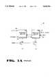
- FIG. 1ais a simplified representation of a dual differential amplifier commonly used in the prior art sense amplifier 20.
- differential amplifier 200with differential inputs 205, 215 and single output 206 is controlled by transistor 207.
- differential amplifier 210which receives differential inputs 205, 215 to generate output-bar 216.
- the sense amplifieris turned on by an enable signal which drives the gates of transistors 207 and 217.
- FIG. 1bis a schematic diagram of prior art sense amplifier 20.
- a typical sense amplifier 30comprises two differential amplifiers 31, 32.
- Input 307 and input-bar 317are applied to the gates of the differential pair of transistors 303, 302, respectively in differential amplifier 31.
- input 307 and input-bar 317apply to the gates of the differential pair of transistors 312, 313, respectively in differential amplifier 32.
- Tail device 304 in differential amplifier 31is driven by the node connecting the gates of p-channel gate-coupled devices 300,301.
- tail device 314is driven by the node connecting the gates of p-channel gate-coupled devices 310, 311 in differential amplifier 32.
- the prior art sense amplifiershave the following shortcomings. First, these sense amplifiers cannot accept input signals at the power supply voltage (e.g., V cc ). Specifically, the input signals must be translated down from the power supply voltage to a lower voltage (e.g., 1 V below V cc ) for the prior art circuits to work properly. Moreover, the gain of the pre-amplifier stage of these prior art circuits is high which increases the delay through the amplifier.
- the improved sense amplifier of the present inventionincludes a level shifting circuit that has a first input for receiving a true signal (IN) and a second input for receiving a complement signal (IN-bar).
- the level shifting circuitis coupled to a pre-amplification circuit that provides voltage gain to the true and complement signals.
- the pre-amplification circuithas a first output for generating an amplified true signal and a second output for generating an amplified complement signal.
- the improved sense amplifier of the present inventionalso includes a first driver circuit (e.g., an inverter), coupled to the pre-amplification circuit, having an input for receiving the amplified complement signal and an output for generating the output signal (i.e., the output of the first driver is coupled to the output port (V out ) of the sense amplifier).
- the first driveralso includes a first port for receiving a first reference voltage, usually a power voltage signal, and a second port for receiving a second reference voltage, usually a ground signal.
- the present inventionalso includes a second driver (e.g., an inverter) that is coupled to the pre-amplification circuit. This second driver includes an input port for receiving the amplified true signal and an output port.
- This second driveralso includes a first port for receiving the power supply voltage signal and a second port for receiving the ground signal.
- the second driverprovides high gain for the sense amplifier.
- the present inventionalso includes a first transistor that has a first electrode (e.g., a drain) coupled to the first reference voltage (e.g., the power supply voltage), a second electrode (e.g., a source) coupled to the first port of the first and second inverters and a third electrode (e.g., gate), which is employed to control current flow through the transistor.
- a second transistorhas a first electrode coupled to the second port of the first and second inverters, a second electrode coupled to the second reference voltage (e.g., a ground signal) and a third electrode coupled to the output of the second inverter and the third electrode of the first and second transistor.
- the improved sense amplifier of the present inventionhas several distinct advantages over the prior art sense amplifiers.
- the amplifier of the present inventionaccepts input signals at the power supply voltage.
- the pre-amplifier of the present inventionhas a minimum number of transistors to minimize the input offset voltage.
- the pre-amplifier of the present inventionhas low gain to minimize the propagation delay through the amplifier.
- the second stage of the present inventionhas high voltage gain.
- FIG. 1ais a simplified representation of a dual differential amplifier with differential outputs commonly used in the prior art sense amplifiers.
- FIG. 1bis a schematic diagram of the prior art sense amplifier of FIG. 1a.
- FIG. 2illustrates a schematic diagram of the present invention.
- FIG. 3illustrates a circuit diagram of the present invention.
- FIG. 4illustrates a sense amplifier propagation delay versus the supply voltage.
- FIG. 5illustrates a graph of V in versus V out for the first stage of the present invention and also the gain of the improved sense amp of the present invention.
- MOSMetal Oxide Semiconductor
- a transistorhas a first electrode, a second electrode, and a third electrode.
- the first electrodemay be a source or a drain depending on the type of transistor employed.
- the second electrodeis a drain or source, whichever the first electrode is not.
- the third electrodeis a gate of the transistor that is employed to control the amount of current flowing through the transistor.
- the first and second electrodesform a current path for the transistor. In an NMOS transistor current flows from the drain to the source, whereas in a PMOS transistor, the current flows from the source to the drain.
- the first electrode and the second electrodemay be a collector or an emitter
- the third electrodemay be a base in a bipolar transistor.
- the collector and emitter in a bipolar transistorperform essentially the same function as the drain and source in a MOS transistor. Specifically, the collector and emitter form a current path for the bipolar transistor, and the base is employed to control the amount of current flowing through the current path.
- FIG. 2illustrates a schematic diagram of the present invention.
- the present inventionis an improved two-stage differential sense amplifier with positive feedback in the first stage 21 and the second stage 34.
- the first stage 21includes a level shifting and pre-amplification circuit for receiving the differential inputs (IN and IN) and generating amplified true and complement signals.
- the second stage 34includes a first driver, which in this embodiment of the present invention is a first inverter 23 that is coupled to the level shifting and pre-amplification circuit of the first stage 21.
- the first inverter 23includes an input for receiving an amplified complement signal (IN), and an output coupled to the output port (V out ) of the sense amplifier.
- the second stage 34also includes a second driver, which in this embodiment of the present invention is a second inverter 27 that is also coupled to the level shifting and pre-amplification circuit of the first stage 21.
- the second inverter 27has an input for receiving the amplified true signal (IN) and also has an output port.
- Both the first inverter 23 and the second inverter 27each have a first port for receiving a first reference voltage, such as a power voltage signal and a second port for receiving a second reference voltage, such as a V ss signal (e.g. ground signal).
- the first ports of the first and second inverters 23 and 27are coupled to the first reference voltage (e.g., V cc ) through a first transistor M7.
- transistor M7is a PMOS transistor.
- the ground port of the first and second inverters 23 and 27is coupled to the V ss (e.g., ground) via a second transistor M10.
- transistor M10is a MMOS transistor.
- the gates of transistors M7 and M10are coupled to the output port of the second inverter 27.
- FIG. 3illustrates in greater detail the circuit elements of the present invention.
- the small circle on transistorse.g., MS, M6 and M7 indicates that it is a p-channel transistor.
- Transistorse.g., M1-M4, M8-10) without the small circle are, thus, n-channel transistors.
- Transistors M5 and M8, as well as transistors M6 and M9,are complementary transistor pairs.
- the gates of transistors M5 and M8are connected together and also connected to node 2, as shown.
- the drains of transistors M5 and M8are coupled together and also connected to the output port (V out ).
- the sources of transistors M5 and M8connect respectively to node 4 and node 5.
- the drains of transistors M6 and M9are coupled together and also connected to node 3.
- the source of transistor M6 and the source of transistor M9connect respectively to node 4 and node 5.
- the first stage 21 of the present inventionincludes transistors M1 and M2 for receiving the true and complement signals, respectively.
- Transistors M1 and M2are known in the art as “source followers” that have their drains coupled to the power supply voltage (V cc ) and their sources coupled to the inputs for the second stage 34.
- the source of transistor M1is coupled to node 1 which is coupled to the gates of transistors M6 and M9 of the second stage 34.
- the source of transistor M2is coupled to node 2, which is coupled to gates of transistors M5 and M8 of the second stage 34.
- the first stage 21also includes transistors M3 and M4 that are cross-coupled (i.e., having their gates tied to the drains of each other). Transistors M1 and M2 act as loads for transistors M3 and M4 in the first stage 21. Transistors M3 and M4 are connected in a positive feedback loop which provides gain for the first stage 21. Nodes 1 and 2 are outputs of the first stage 21 and inputs to the second stage 34.
- the source followers M1 and M2set the common mode voltage at node 1 and node 2 at approximately 1/2 the value of V cc . Hence, transistors M1 and M2 provide a "level-shifting" function to establish the input voltages to the second stage 34.
- Table 1illustrates exemplary W/L values for the transistors employed in the present invention.
- Wrepresents the width of the gate of the transistor in question, and L represents the length of the gate of that particular transistor. Unless otherwise noted, the W and L values are expressed in micron units (um).
- the W and L ratios illustrated in Table 1are exemplary values that may be appropriate for certain applications.
- transistors M1-M4are sized using a 1 micron gate length. Although using a 1 micron gate length slightly increases the propagation delay through this part (i.e., slows the performance of this particular part), the use of the 1 micron gate length lowers the amount of current entering the second stage 34 and also provides a better matching of transistors M1-M4, which is useful for the proper operation of the present invention. Please refer to Table 1 for exemplary values of transistors M1-M4 that provide a proper "level-shifting" of nodes 1 and 2.
- the second stage 34includes a first inverter 23 made up of transistors M5 and M8.
- the gates of M5 and M8are coupled to node 2, which reflects an amplified complement signal. If node were tied to ground or V ss and node 4 was tied to V cc , the first inverter 23, including transistors M5 and M8, would provide an approximate gain of ten in one embodiment.
- the output port (V out ) of the present inventionis coupled to the drain of transistor M8 and the drain of transistor M5 (i.e., the output of the first inverter 23).
- the second stage 34includes a second inverter 27 that includes transistors M6 and M9.
- the second inverter 27,if coupled to the rails (V cc and V ss ), would also produce an approximate gain of ten in one embodiment.
- the present inventionties the output of the second inverter 27 to the gates of M7 and M10.
- Transistor M10provides a path to ground for node 5. Specifically, the drain of M10 is coupled to node 5, and the source of M10 is coupled to V ss (e.g., ground).
- Transistor M7provides a path for node 4 to V cc . Specifically, the source of transistor M7 is coupled to V cc and the drain is coupled to node 4.
- the present inventionutilizes the combination of transistors M6, M7, M9 and M10 to greatly increase the gain of the first inverter. This gain is generated by feeding back the output of the second inverter, which has as its input the amplified true signal (node 1) to the first inverter (M5 and M8) through transistors M7 and M10.
- FIG. 4illustrates a graph of the propagation delay of the present invention versus the power supply voltage (V cc ).
- FIG. 4illustrates results for a sense amplifier employing transistors sized in accordance with the values as specified in Table 1. The actual results may differ based on the process technology.
- the graphs in this applicationwere generated using a circuit simulator.
- the propagation delay through the sense amplifier in pico seconds (ps)decreases with an increasing power voltage supply (V cc ).
- V ccpower voltage supply
- the propagation delay through the sense amplifieris approximately 1,200 pico seconds at a supply voltage of 2.7 V
- the propagation delay through the sense amplifieris approximately 700 pico seconds at a supply voltage of 3.9 V.
- the propagation delay through the sense amplifieris highly dependent on the process used. For example, it is well known in the art that the speed of a part (i.e., the propagation delay through the part) is directly proportional to the size of the gates of the transistors used. For example, if the width of a gate is halved, the part, as a rule of thumb, is twice as fast.
- the propagation delayis measured from the time the differential inputs cross to the time that the voltage at the output reaches 50% of the full range swing (i.e., V cc -V ss ).
- the propagation delayis generally measured with an input of 100 millivolts (mV).
- mVmillivolts
- FIG. 5illustrates a graph of the V in versus V out (i.e., gain) of the first stage 21 of the present invention, as well as the overall gain of the improved sense amplifier.
- the gain through the first stageis approximately 4-5, whereas the gain through the sense amplifier, as a whole, is approximately 100-200.
- the vertical axis representing V outis divided into 0.5 V increments, and V in (the horizontal axis) is divided into 10 millivolts (mV) increments.
- mVmillivolts
- the gain of an amplifieris simply V out /V in .
- the results said forth in FIG. 5illustrates the gain of one exemplary embodiment of the present invention that employs transistors, which have the sizes illustrated in Table 1. The actual results with respect to the overall gain of the present invention may differ depending on the parameters discussed previously.
Landscapes
- Amplifiers (AREA)
Abstract
Description
TABLE 1 ______________________________________ Transistor W/L ______________________________________ M1 8/1 M2 8/1 M3 8/1 M4 8/1 M5 8/0.5 M6 8/0.5 M7 8/0.5M8 5/0.5M9 5/0.5M10 5/0.5 ______________________________________
Claims (5)
Priority Applications (1)
| Application Number | Priority Date | Filing Date | Title |
|---|---|---|---|
| US08/578,187US5640356A (en) | 1995-12-29 | 1995-12-29 | Two-stage differential sense amplifier with positive feedback in the first and second stages |
Applications Claiming Priority (1)
| Application Number | Priority Date | Filing Date | Title |
|---|---|---|---|
| US08/578,187US5640356A (en) | 1995-12-29 | 1995-12-29 | Two-stage differential sense amplifier with positive feedback in the first and second stages |
Publications (1)
| Publication Number | Publication Date |
|---|---|
| US5640356Atrue US5640356A (en) | 1997-06-17 |
Family
ID=24311796
Family Applications (1)
| Application Number | Title | Priority Date | Filing Date |
|---|---|---|---|
| US08/578,187Expired - LifetimeUS5640356A (en) | 1995-12-29 | 1995-12-29 | Two-stage differential sense amplifier with positive feedback in the first and second stages |
Country Status (1)
| Country | Link |
|---|---|
| US (1) | US5640356A (en) |
Cited By (26)
| Publication number | Priority date | Publication date | Assignee | Title |
|---|---|---|---|---|
| WO1999014758A1 (en)* | 1997-09-16 | 1999-03-25 | Intel Corporation | Sense amplifier for flash memories |
| US5982690A (en)* | 1998-04-15 | 1999-11-09 | Cirrus Logic, Inc. | Static low-power differential sense amplifier circuits, systems and methods |
| US6088278A (en)* | 1998-07-23 | 2000-07-11 | Micron Technology, Inc. | Latching sense amplifier structure with pre-amplifier |
| US6108258A (en)* | 1999-08-19 | 2000-08-22 | United Integrated Circuits Corp. | Sense amplifier for high-speed integrated circuit memory device |
| US6259633B1 (en)* | 1999-10-19 | 2001-07-10 | Advanced Micro Devices, Inc. | Sense amplifier architecture for sliding banks for a simultaneous operation flash memory device |
| US20020130692A1 (en)* | 1999-06-28 | 2002-09-19 | Broadcom Corporation | Current-controlled CMOS logic family |
| US20030067337A1 (en)* | 1999-06-28 | 2003-04-10 | Broadcom Corporation | Current-controlled CMOS circuit using higher voltage supply in low voltage CMOS process |
| US20030122603A1 (en)* | 2000-02-24 | 2003-07-03 | Broadcom Corporation | Current-controlled CMOS circuits with inductive broadbanding |
| US6639866B2 (en) | 2000-11-03 | 2003-10-28 | Broadcom Corporation | Very small swing high performance asynchronous CMOS static memory (multi-port register file) with power reducing column multiplexing scheme |
| US6897697B2 (en)* | 1999-06-28 | 2005-05-24 | Broadcom Corporation | Current-controlled CMOS circuit using higher voltage supply in low voltage CMOS process |
| US7126869B1 (en) | 2003-06-26 | 2006-10-24 | Cypress Semiconductor Corp. | Sense amplifier with dual cascode transistors and improved noise margin |
| US20070024369A1 (en)* | 2005-07-29 | 2007-02-01 | Jun Cao | Current-controlled CMOS (C3MOS) wideband input data amplifier for reduced differential and common-mode reflection |
| US20070025435A1 (en)* | 2005-07-29 | 2007-02-01 | Jun Cao | Current-controlled CMOS (C3MOS) fully differential integrated wideband amplifier/equalizer with adjustable gain and frequency response without additional power or loading |
| US20070052467A1 (en)* | 2005-09-06 | 2007-03-08 | Jun Cao | Current-controlled CMOS (C3MOS) fully differential integrated delay cell with variable delay and high bandwidth |
| US20070097765A1 (en)* | 2005-10-28 | 2007-05-03 | Sony Corporation | Dynamic sense amplifier for SRAM |
| US7330388B1 (en) | 2005-09-23 | 2008-02-12 | Cypress Semiconductor Corporation | Sense amplifier circuit and method of operation |
| US7849208B2 (en) | 2002-08-30 | 2010-12-07 | Broadcom Corporation | System and method for TCP offload |
| US7912064B2 (en) | 2002-08-30 | 2011-03-22 | Broadcom Corporation | System and method for handling out-of-order frames |
| US7934021B2 (en) | 2002-08-29 | 2011-04-26 | Broadcom Corporation | System and method for network interfacing |
| US8116203B2 (en) | 2001-07-23 | 2012-02-14 | Broadcom Corporation | Multiple virtual channels for use in network devices |
| US8135016B2 (en) | 2002-03-08 | 2012-03-13 | Broadcom Corporation | System and method for identifying upper layer protocol message boundaries |
| US8180928B2 (en) | 2002-08-30 | 2012-05-15 | Broadcom Corporation | Method and system for supporting read operations with CRC for iSCSI and iSCSI chimney |
| US20120235708A1 (en)* | 2011-03-16 | 2012-09-20 | Mark Slamowitz | Method and System for High Speed Differential Synchronous Sense Amplifier |
| US8402142B2 (en) | 2002-08-30 | 2013-03-19 | Broadcom Corporation | System and method for TCP/IP offload independent of bandwidth delay product |
| US8750320B2 (en) | 1997-01-23 | 2014-06-10 | Broadcom Corporation | Fibre channel arbitrated loop bufferless switch circuitry to increase bandwidth without significant increase in cost |
| US8798091B2 (en) | 1998-11-19 | 2014-08-05 | Broadcom Corporation | Fibre channel arbitrated loop bufferless switch circuitry to increase bandwidth without significant increase in cost |
Citations (2)
| Publication number | Priority date | Publication date | Assignee | Title |
|---|---|---|---|---|
| US4618785A (en)* | 1984-09-06 | 1986-10-21 | Thomson Components - Mostek Corporation | CMOS sense amplifier with level shifter |
| US5231318A (en)* | 1990-08-03 | 1993-07-27 | Reddy Chitranjan N | Differential latch sense amplifier |
- 1995
- 1995-12-29USUS08/578,187patent/US5640356A/ennot_activeExpired - Lifetime
Patent Citations (2)
| Publication number | Priority date | Publication date | Assignee | Title |
|---|---|---|---|---|
| US4618785A (en)* | 1984-09-06 | 1986-10-21 | Thomson Components - Mostek Corporation | CMOS sense amplifier with level shifter |
| US5231318A (en)* | 1990-08-03 | 1993-07-27 | Reddy Chitranjan N | Differential latch sense amplifier |
Cited By (58)
| Publication number | Priority date | Publication date | Assignee | Title |
|---|---|---|---|---|
| US8750320B2 (en) | 1997-01-23 | 2014-06-10 | Broadcom Corporation | Fibre channel arbitrated loop bufferless switch circuitry to increase bandwidth without significant increase in cost |
| US8767756B2 (en) | 1997-01-23 | 2014-07-01 | Broadcom Corporation | Fibre channel arbitrated loop bufferless switch circuitry to increase bandwidth without significant increase in cost |
| US8774199B2 (en) | 1997-01-23 | 2014-07-08 | Broadcom Corporation | Fibre channel arbitrated loop bufferless switch circuitry to increase bandwidth without significant increase in cost |
| KR100382693B1 (en)* | 1997-09-16 | 2003-05-09 | 인텔 코오퍼레이션 | Sense amplifier for flash memories |
| US5973957A (en)* | 1997-09-16 | 1999-10-26 | Intel Corporation | Sense amplifier comprising a preamplifier and a differential input latch for flash memories |
| WO1999014758A1 (en)* | 1997-09-16 | 1999-03-25 | Intel Corporation | Sense amplifier for flash memories |
| US5982690A (en)* | 1998-04-15 | 1999-11-09 | Cirrus Logic, Inc. | Static low-power differential sense amplifier circuits, systems and methods |
| US6088278A (en)* | 1998-07-23 | 2000-07-11 | Micron Technology, Inc. | Latching sense amplifier structure with pre-amplifier |
| US8798091B2 (en) | 1998-11-19 | 2014-08-05 | Broadcom Corporation | Fibre channel arbitrated loop bufferless switch circuitry to increase bandwidth without significant increase in cost |
| US6900670B2 (en) | 1999-06-28 | 2005-05-31 | Broadcom Corporation | Current-controlled CMOS logic family |
| US20020130692A1 (en)* | 1999-06-28 | 2002-09-19 | Broadcom Corporation | Current-controlled CMOS logic family |
| US8299834B2 (en) | 1999-06-28 | 2012-10-30 | Broadcom Corporation | Current-controlled CMOS logic family |
| US7724057B2 (en) | 1999-06-28 | 2010-05-25 | Broadcom Corporation | Current-controlled CMOS logic family |
| US20030001646A1 (en)* | 1999-06-28 | 2003-01-02 | Broadcom Corporation | Current-controlled CMOS logic family |
| US20030067337A1 (en)* | 1999-06-28 | 2003-04-10 | Broadcom Corporation | Current-controlled CMOS circuit using higher voltage supply in low voltage CMOS process |
| US6897697B2 (en)* | 1999-06-28 | 2005-05-24 | Broadcom Corporation | Current-controlled CMOS circuit using higher voltage supply in low voltage CMOS process |
| US8823435B2 (en) | 1999-06-28 | 2014-09-02 | Broadcom Corporation | Current-controlled CMOS logic family |
| US9112487B2 (en) | 1999-06-28 | 2015-08-18 | Broadcom Corporation | Current-controlled CMOS logic family |
| US6911855B2 (en) | 1999-06-28 | 2005-06-28 | Broadcom Corporation | Current-controlled CMOS circuit using higher voltage supply in low voltage CMOS process |
| US6937080B2 (en) | 1999-06-28 | 2005-08-30 | Broadcom Corporation | Current-controlled CMOS logic family |
| US10396763B2 (en) | 1999-06-28 | 2019-08-27 | Avago Technologies International Sales Pte. Limited | Current-controlled CMOS logic family |
| US9831853B2 (en) | 1999-06-28 | 2017-11-28 | Avago Technologies General Ip (Singapore) Pte. Ltd. | Current-controlled CMOS logic family |
| US6108258A (en)* | 1999-08-19 | 2000-08-22 | United Integrated Circuits Corp. | Sense amplifier for high-speed integrated circuit memory device |
| US6259633B1 (en)* | 1999-10-19 | 2001-07-10 | Advanced Micro Devices, Inc. | Sense amplifier architecture for sliding banks for a simultaneous operation flash memory device |
| US20030122603A1 (en)* | 2000-02-24 | 2003-07-03 | Broadcom Corporation | Current-controlled CMOS circuits with inductive broadbanding |
| US7919985B2 (en) | 2000-02-24 | 2011-04-05 | Broadcom Corporation | Current-controlled CMOS circuits with inductive broadbanding |
| US6909309B2 (en) | 2000-02-24 | 2005-06-21 | Broadcom Corporation | Current-controlled CMOS circuits with inductive broadbanding |
| US7251175B2 (en) | 2000-11-03 | 2007-07-31 | Broadcom Corporation | Very small swing high performance asynchronous CMOS static memory (multi-port register file) with power reducing column multiplexing scheme |
| US6822918B2 (en) | 2000-11-03 | 2004-11-23 | Broadcom Corporation | Very small swing high performance asynchronous CMOS static memory (multi-port register file) with power reducing column multiplexing scheme |
| US20050091477A1 (en)* | 2000-11-03 | 2005-04-28 | Mark Slamowitz | Very small swing high performance asynchronous CMOS static memory (multi-port register file) with power reducing column multiplexing scheme |
| US20040066687A1 (en)* | 2000-11-03 | 2004-04-08 | Mark Slamowitz | Very small swing high performance asynchronous CMOS static memory (multi-port register file) with power reducing column multiplexing scheme |
| US6639866B2 (en) | 2000-11-03 | 2003-10-28 | Broadcom Corporation | Very small swing high performance asynchronous CMOS static memory (multi-port register file) with power reducing column multiplexing scheme |
| US8493857B2 (en) | 2001-07-23 | 2013-07-23 | Broadcom Corporation | Multiple logical channels for use in network devices |
| US8116203B2 (en) | 2001-07-23 | 2012-02-14 | Broadcom Corporation | Multiple virtual channels for use in network devices |
| US9036643B2 (en) | 2001-07-23 | 2015-05-19 | Broadcom Corporation | Multiple logical channels for use in network devices |
| US8345689B2 (en) | 2002-03-08 | 2013-01-01 | Broadcom Corporation | System and method for identifying upper layer protocol message boundaries |
| US8451863B2 (en) | 2002-03-08 | 2013-05-28 | Broadcom Corporation | System and method for identifying upper layer protocol message boundaries |
| US8958440B2 (en) | 2002-03-08 | 2015-02-17 | Broadcom Corporation | System and method for identifying upper layer protocol message boundaries |
| US8135016B2 (en) | 2002-03-08 | 2012-03-13 | Broadcom Corporation | System and method for identifying upper layer protocol message boundaries |
| US7934021B2 (en) | 2002-08-29 | 2011-04-26 | Broadcom Corporation | System and method for network interfacing |
| US8549152B2 (en) | 2002-08-30 | 2013-10-01 | Broadcom Corporation | System and method for TCP/IP offload independent of bandwidth delay product |
| US7912064B2 (en) | 2002-08-30 | 2011-03-22 | Broadcom Corporation | System and method for handling out-of-order frames |
| US7849208B2 (en) | 2002-08-30 | 2010-12-07 | Broadcom Corporation | System and method for TCP offload |
| US8402142B2 (en) | 2002-08-30 | 2013-03-19 | Broadcom Corporation | System and method for TCP/IP offload independent of bandwidth delay product |
| US7929540B2 (en) | 2002-08-30 | 2011-04-19 | Broadcom Corporation | System and method for handling out-of-order frames |
| US8180928B2 (en) | 2002-08-30 | 2012-05-15 | Broadcom Corporation | Method and system for supporting read operations with CRC for iSCSI and iSCSI chimney |
| US8677010B2 (en) | 2002-08-30 | 2014-03-18 | Broadcom Corporation | System and method for TCP offload |
| US7126869B1 (en) | 2003-06-26 | 2006-10-24 | Cypress Semiconductor Corp. | Sense amplifier with dual cascode transistors and improved noise margin |
| US7362174B2 (en) | 2005-07-29 | 2008-04-22 | Broadcom Corporation | Current-controlled CMOS (C3MOS) wideband input data amplifier for reduced differential and common-mode reflection |
| US7598811B2 (en) | 2005-07-29 | 2009-10-06 | Broadcom Corporation | Current-controlled CMOS (C3MOS) fully differential integrated wideband amplifier/equalizer with adjustable gain and frequency response without additional power or loading |
| US20070025435A1 (en)* | 2005-07-29 | 2007-02-01 | Jun Cao | Current-controlled CMOS (C3MOS) fully differential integrated wideband amplifier/equalizer with adjustable gain and frequency response without additional power or loading |
| US20070024369A1 (en)* | 2005-07-29 | 2007-02-01 | Jun Cao | Current-controlled CMOS (C3MOS) wideband input data amplifier for reduced differential and common-mode reflection |
| US7598788B2 (en) | 2005-09-06 | 2009-10-06 | Broadcom Corporation | Current-controlled CMOS (C3MOS) fully differential integrated delay cell with variable delay and high bandwidth |
| US20070052467A1 (en)* | 2005-09-06 | 2007-03-08 | Jun Cao | Current-controlled CMOS (C3MOS) fully differential integrated delay cell with variable delay and high bandwidth |
| US7330388B1 (en) | 2005-09-23 | 2008-02-12 | Cypress Semiconductor Corporation | Sense amplifier circuit and method of operation |
| US7313040B2 (en) | 2005-10-28 | 2007-12-25 | Sony Corporation | Dynamic sense amplifier for SRAM |
| US20070097765A1 (en)* | 2005-10-28 | 2007-05-03 | Sony Corporation | Dynamic sense amplifier for SRAM |
| US20120235708A1 (en)* | 2011-03-16 | 2012-09-20 | Mark Slamowitz | Method and System for High Speed Differential Synchronous Sense Amplifier |
Similar Documents
| Publication | Publication Date | Title |
|---|---|---|
| US5640356A (en) | Two-stage differential sense amplifier with positive feedback in the first and second stages | |
| US4973864A (en) | Sense circuit for use in semiconductor memory | |
| KR100735754B1 (en) | Sense amp flip flop | |
| US4999519A (en) | Semiconductor circuit with low power consumption having emitter-coupled logic or differential amplifier | |
| US5821799A (en) | Low voltage level shifting circuit and low voltage sense amplifier | |
| US4618785A (en) | CMOS sense amplifier with level shifter | |
| US5537066A (en) | Flip-flop type amplifier circuit | |
| US5247479A (en) | Current sensing amplifier for SRAM | |
| US5467313A (en) | Level shifter and data output buffer having same | |
| US5345121A (en) | Differential amplification circuit | |
| EP0090572B1 (en) | Semiconductor sense-amplifier circuitry | |
| JPH06132747A (en) | Semiconductor device | |
| US5414379A (en) | Output buffer circuit for integrated circuit | |
| US5091886A (en) | Dual current data bus clamp circuit of semiconductor memory device | |
| JP2756797B2 (en) | FET sense amplifier | |
| US4658160A (en) | Common gate MOS differential sense amplifier | |
| US5606292A (en) | Ring oscillator having its output amplified in a comparator | |
| US5260904A (en) | Data bus clamp circuit for a semiconductor memory device | |
| US4908794A (en) | Semiconductor memory device with improved output circuit | |
| US4626713A (en) | Trip-point clamping circuit for a semiconductor device | |
| US5646892A (en) | Data reading circuit | |
| US6295242B1 (en) | SRAM with current-mode test read data path | |
| KR100762866B1 (en) | Dual power supply circuit of sense amplifier | |
| JPH04160815A (en) | Output buffer circuit | |
| JP2638046B2 (en) | I/O line load circuit |
Legal Events
| Date | Code | Title | Description |
|---|---|---|---|
| AS | Assignment | Owner name:CYPRESS SEMICONDUCTOR, CALIFORNIA Free format text:ASSIGNMENT OF ASSIGNORS INTEREST;ASSIGNOR:GIBBS, GARY A.;REEL/FRAME:007937/0006 Effective date:19960313 | |
| STCF | Information on status: patent grant | Free format text:PATENTED CASE | |
| FPAY | Fee payment | Year of fee payment:4 | |
| SULP | Surcharge for late payment | ||
| REMI | Maintenance fee reminder mailed | ||
| FPAY | Fee payment | Year of fee payment:8 | |
| FEPP | Fee payment procedure | Free format text:PAYER NUMBER DE-ASSIGNED (ORIGINAL EVENT CODE: RMPN); ENTITY STATUS OF PATENT OWNER: LARGE ENTITY Free format text:PAYOR NUMBER ASSIGNED (ORIGINAL EVENT CODE: ASPN); ENTITY STATUS OF PATENT OWNER: LARGE ENTITY | |
| REMI | Maintenance fee reminder mailed | ||
| FPAY | Fee payment | Year of fee payment:12 | |
| SULP | Surcharge for late payment | Year of fee payment:11 | |
| AS | Assignment | Owner name:RPX CORPORATION, CALIFORNIA Free format text:ASSIGNMENT OF ASSIGNORS INTEREST;ASSIGNOR:CYPRESS SEMICONDUCTOR CORPORATION;REEL/FRAME:033119/0615 Effective date:20140604 | |
| AS | Assignment | Owner name:JPMORGAN CHASE BANK, N.A., AS COLLATERAL AGENT, IL Free format text:SECURITY AGREEMENT;ASSIGNORS:RPX CORPORATION;RPX CLEARINGHOUSE LLC;REEL/FRAME:038041/0001 Effective date:20160226 | |
| AS | Assignment | Owner name:RPX CLEARINGHOUSE LLC, CALIFORNIA Free format text:RELEASE (REEL 038041 / FRAME 0001);ASSIGNOR:JPMORGAN CHASE BANK, N.A.;REEL/FRAME:044970/0030 Effective date:20171222 Owner name:RPX CORPORATION, CALIFORNIA Free format text:RELEASE (REEL 038041 / FRAME 0001);ASSIGNOR:JPMORGAN CHASE BANK, N.A.;REEL/FRAME:044970/0030 Effective date:20171222 |