US5637901A - Integrated circuit with diode-connected transistor for reducing ESD damage - Google Patents
Integrated circuit with diode-connected transistor for reducing ESD damageDownload PDFInfo
- Publication number
- US5637901A US5637901AUS08/468,250US46825095AUS5637901AUS 5637901 AUS5637901 AUS 5637901AUS 46825095 AUS46825095 AUS 46825095AUS 5637901 AUS5637901 AUS 5637901A
- Authority
- US
- United States
- Prior art keywords
- base
- region
- cell
- emitter
- esd
- Prior art date
- Legal status (The legal status is an assumption and is not a legal conclusion. Google has not performed a legal analysis and makes no representation as to the accuracy of the status listed.)
- Expired - Lifetime
Links
- 230000006378damageEffects0.000titleclaimsdescription13
- 239000002019doping agentSubstances0.000claimsdescription10
- 239000000463materialSubstances0.000claimsdescription10
- 238000002955isolationMethods0.000claimsdescription8
- 239000004065semiconductorSubstances0.000claimsdescription6
- 239000003990capacitorSubstances0.000claimsdescription4
- 230000015572biosynthetic processEffects0.000claims2
- 238000009792diffusion processMethods0.000abstractdescription6
- 238000001465metallisationMethods0.000abstractdescription4
- 230000003071parasitic effectEffects0.000abstractdescription4
- 238000010438heat treatmentMethods0.000abstractdescription3
- XUIMIQQOPSSXEZ-UHFFFAOYSA-NSiliconChemical compound[Si]XUIMIQQOPSSXEZ-UHFFFAOYSA-N0.000description8
- 229910052710siliconInorganic materials0.000description8
- 239000010703siliconSubstances0.000description8
- 230000015556catabolic processEffects0.000description5
- 229910021420polycrystalline siliconInorganic materials0.000description4
- 238000012876topographyMethods0.000description4
- VYPSYNLAJGMNEJ-UHFFFAOYSA-NSilicium dioxideChemical compoundO=[Si]=OVYPSYNLAJGMNEJ-UHFFFAOYSA-N0.000description2
- 230000008901benefitEffects0.000description2
- 239000004020conductorSubstances0.000description2
- 238000010586diagramMethods0.000description2
- 239000003989dielectric materialSubstances0.000description2
- 230000005684electric fieldEffects0.000description2
- 239000000758substrateSubstances0.000description2
- 239000010409thin filmSubstances0.000description2
- WPPDFTBPZNZZRP-UHFFFAOYSA-Naluminum copperChemical compound[Al].[Cu]WPPDFTBPZNZZRP-UHFFFAOYSA-N0.000description1
- 238000005513bias potentialMethods0.000description1
- 230000001066destructive effectEffects0.000description1
- 230000001627detrimental effectEffects0.000description1
- 230000000694effectsEffects0.000description1
- 238000009413insulationMethods0.000description1
- 238000004519manufacturing processMethods0.000description1
- 239000002184metalSubstances0.000description1
- 229910052751metalInorganic materials0.000description1
- 230000001681protective effectEffects0.000description1
- 235000012239silicon dioxideNutrition0.000description1
- 239000000377silicon dioxideSubstances0.000description1
- 239000012209synthetic fiberSubstances0.000description1
- 229920002994synthetic fiberPolymers0.000description1
Images


Classifications
- H—ELECTRICITY
- H10—SEMICONDUCTOR DEVICES; ELECTRIC SOLID-STATE DEVICES NOT OTHERWISE PROVIDED FOR
- H10D—INORGANIC ELECTRIC SEMICONDUCTOR DEVICES
- H10D89/00—Aspects of integrated devices not covered by groups H10D84/00 - H10D88/00
- H10D89/60—Integrated devices comprising arrangements for electrical or thermal protection, e.g. protection circuits against electrostatic discharge [ESD]
- H10D89/601—Integrated devices comprising arrangements for electrical or thermal protection, e.g. protection circuits against electrostatic discharge [ESD] for devices having insulated gate electrodes, e.g. for IGFETs or IGBTs
- H10D89/711—Integrated devices comprising arrangements for electrical or thermal protection, e.g. protection circuits against electrostatic discharge [ESD] for devices having insulated gate electrodes, e.g. for IGFETs or IGBTs using bipolar transistors as protective elements
- H—ELECTRICITY
- H10—SEMICONDUCTOR DEVICES; ELECTRIC SOLID-STATE DEVICES NOT OTHERWISE PROVIDED FOR
- H10D—INORGANIC ELECTRIC SEMICONDUCTOR DEVICES
- H10D89/00—Aspects of integrated devices not covered by groups H10D84/00 - H10D88/00
- H10D89/60—Integrated devices comprising arrangements for electrical or thermal protection, e.g. protection circuits against electrostatic discharge [ESD]
- H10D89/601—Integrated devices comprising arrangements for electrical or thermal protection, e.g. protection circuits against electrostatic discharge [ESD] for devices having insulated gate electrodes, e.g. for IGFETs or IGBTs
- H10D89/611—Integrated devices comprising arrangements for electrical or thermal protection, e.g. protection circuits against electrostatic discharge [ESD] for devices having insulated gate electrodes, e.g. for IGFETs or IGBTs using diodes as protective elements
Definitions
- This inventionrelates to the means of reducing ESD damage to integrated circuits (ICs) comprising a substrate carrying a large number of circuit elements such as transistors and the like.
- Electrostatic DischargeESD
- the electrostatic chargecan be developed by any of many sources, such as lightning, friction between insulating bodies such as synthetic fiber clothing, and contact with chip handling apparatus. Damage occurs when the ESD charge is accidentally coupled to one of the circuit terminal points to cause a large pulse of current to flow through some portion of the metal interconnect of the chip to a sensitive circuit element of the IC. Frequently, such current pulses will destroy the circuit element and with it the entire IC chip.
- Bipolar junctions, dielectrics and thin film circuit elementsare especially subject to damage from ESD transients of relatively high energy.
- ESD transientscan be simulated by the so-called Human Body Model (HBM), Machine Model (MM) and Charged Device Model (CDM).
- HBMHuman Body Model
- MMMachine Model
- CDMCharged Device Model
- a high-performance ESD clamp deviceformed as part of the IC chip and connected to terminal points (such as bond pads) of the chip to shunt destructive ESD energy away from sensitive die circuitry.
- This embodimentcomprises a diode-connected vertical bipolar transistor having a collector-emitter-base layout configuration, with circular and annular topographies.
- the two terminal, diode connected bipolar transistor ESD deviceis formed by externally connecting the base and emitter together with die metallization. A symbolic representation can be found in FIG. 1.
- This two terminal clamp deviceis arranged to be connected between supply rails, ground, or any other circuit nodes. That is, the clamp device is connected as a shunt element and formed to withstand large power transients such as encountered during an ESD event between the external terminal point (bond pad and package pin) and sensitive circuitry to be protected. When an electrostatic pulse of large energy strikes the chip pin, the clamp device conducts to shunt the ESD energy away from sensitive circuitry. Thus the ESD energy is dissipated so as to avoid damaging any sensitive circuit elements connected to the external terminal point.
- ESD clamp deviceis its improved capability to conduct current vertically from emitter to collector identical to a bipolar transistor in the active mode. This result is accomplished by the position of the emitter which encloses the base contact. Further features comprise circular and annular topographies which eliminate high electric field concentrations and distribute current more evenly throughout the device.
- the active emitter areais increased significantly with only a small increase in transistor area. This gives an important reduction in power density during an ESD event, thus reducing local joule heating and increasing the overall ESD tolerance. Because there is only a small increase in area, the parasitic capacitance is virtually unchanged as compared to non-annular, non-circular clamping devices.
- FIG. 1shows symbolic representations of bipolar transistor ESD devices configured as two terminal devices.
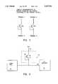
- FIG. 2is a plan view of an IC cell comprising an ESD clamp device in accordance with the present invention
- FIG. 3is a cross-section view of the cell taken along line 3--3 of FIG. 2;
- FIG. 4is a horizontal section of the cell taken along line 4--4 of FIG. 3;
- FIG. 5is a circuit diagram showing the preferred embodiment a clamp device connected in shunt fashion between a bond pad and the IC circuitry to be protected from ESD pulses;
- FIG. 6is a cut-away diagram showing, partly in perspective, current paths during reverse-bias operation.
- the ESD clampis a circular cell generally identified at 10 which is a vertical NPN transistor. Surrounding this cell are other cells of the IC (not shown) formed with devices such as but not limited to transistors, capacitors and resistors.
- the interior of the cell 10comprises silicon isolated from the rest of the chip by dielectric material.
- the outermost region of the ESD cell 10is a dielectrically filled deep trench 12 which functions as electrical isolation for the cell.
- the trench 12circumscribes the ESD cell and extends from the upper silicon surface 8 to the buried oxide layer 14.
- the bottom of the cellis defined by the oxide insulation layer 14 (buried oxide) which is between the lower surface of N-type silicon (to be described) and the upper surface of a P-type silicon substrate (not completely shown), and which sometimes is referred to as the "handle" of the chip.
- the upper surface of the cellis formed of silicon dioxide 16 for the chip.
- the regions 18 outside of the trenchtypically are tied to a supply rail of the chip and are designated as non-active circuit areas.
- the collector region of the ESD cellis comprised of four different diffusions of N-type dopant. They are: a buried layer 20, a deep plug 24, an N-well 22, and a shallow N++ region 26.
- the buried layer 20is a heavily doped region of relatively low resistance which comprises the bottommost electrically active layer of the transistor.
- the buried layer 20extends throughout the ESD cell to the edge of the deep trench 12.
- An annular ring of deep plug 24extends from the silicon surface 8 to the buried layer 20 with its outermost edge abutting the edge of the trench 12.
- the inner edge of the deep plug annulus 24is spaced sufficiently far from the base region 32 of the transistor to assure an adequate breakdown potential of the collector to base junction. Electrical contact to the collector is made through the surface dielectric 16 to an annular-shaped (but not completely closed) highly doped n++ layer 26 concentric with and contained within the deep plug annulus 24.
- the base 32 of the transistoris circular shaped and concentric with the collector plug annulus.
- the base 32is made of P-type dopant (opposite that of the collector) and extends from the silicon surface 8 to a depth that is spaced sufficiently far from the buried layer 20 to assure an adequate breakdown potential between the collector to base regions, and between the collector to emitter regions.
- Electrical contact to the base region 32is made through the surface dielectric 16 to a circular shaped region of a highly doped P++ layer 36 which is concentric to the base 32.
- the P++ layer 36assures good electrical contact to the base region 32 and is constrained on all sides by the base layer 32.
- the emitter 34is a heavily doped N-type layer of annular shape, concentric to the base 32, with its inner edge spaced sufficiently far away from the highly doped P++ layer 36 to assure adequate breakdown potential of the emitter to base junction.
- the outer edge of the emitter annulus 34is located within the base region 32 and spaced sufficiently far from the edge of the base to assure adequate electrical breakdown between the emitter to collector junction. Electrical contact to the emitter 34 is made through the surface dielectric 16.
- the region of silicon 22 surrounding the base 32 and located between the collector plug regions 24 and the buried layer 20is lightly doped N-type (N-well).
- the N-wellis formed by counter doping the P-type epitaxial layer.
- the electrical contacts to the emitter 34 and collector 26are made through openings in the surface dielectric 16 filled with polycrystalline silicon 42, 28 highly doped N-type. Electrical contact to the base region 36 is made through an opening in the surface dielectric 16 filled with polycrystalline silicon 40 of highly doped P-type.
- the polycrystalline silicon layers 42, 28, 40provide good ohmic contact and low resistance between the chip metallization 30, 44 and the silicon surface of the transistor. Above and directly in contact with the polycrystalline silicon layers 42, 28, 40 is chip metallization 30, 44 (e.g., aluminum-copper) providing for external connections.
- the common base-emitter regions 32, 34 of the clamp device 10are connected to the lead 50 extending from sensitive integrated circuitry 52 to a bond pad 54 of the chip.
- Bond pad 54is the interface between the IC chip and the external world.
- the collector 24 of the clamp deviceis connected to the most positive potential which in this embodiment is a power supply rail designated +V s , and serving as a low impedance bus for the clamp device.
- ESD failures in the semiconductor materialare thermally related and proportional to the localized power density in the device. Failures predominately occur in reverse-biased junctions where the power density is equal to the electric field across the junction multiplied by the current density in that semiconductor region.
- Traditional ESD clampsrely on current flows similar to I 1 alone; hence large topographical areas are needed to reduce current density to increase the ESD threshold.
- the area in current path I 2is approximately the topographic area of the emitter diffusion (A e )
- the area in current path I 1is approximated by the topographical circumference of the base diffusion (C base ) multiplied by the base junction depth (X jb ). In most IC chips junction depth is typically much less than emitter drawn feature size. Therefore for the same size transistor:
- the circular and annular topographies of the disclosed deviceprovide for a more uniform and reduced current density compared to more traditional rectangular striped configurations.
- the ESD protection circuit of the disclosed devicealso protects against ESD induced spikes of positive polarity.
- a positive voltage spike generated by an ESDimpinges across wire-bonding pad 50 and power supply conductor 51 as in FIG. 5.
- the potential at the wire bonding pad 50is more positive than the potential at power supply conductor 51.
- Transistor 10responds swiftly with its base-collector junction forward biasing conducting current laterally from base 32 to collector 24 in a manner similar to current I 1 shown in FIG. 6, but in an opposite direction.
- the voltage across the base-emitter junctionis a normal diode drop which is about 0.6 Volt in the preferred embodiment.
- Powerwhich is equal to the product of voltage and current, is small in this case.
- the lateral current flowconsequently does not result in excessive localized heating, hence large ESD thresholds are obtained.
- the ESD clampfunctions as a reverse-biased diode.
- the low parasitic capacitance, low leakage current, and compact geometric area of the ESD clampare important advantageous features of ESD clamps for high speed applications.
Landscapes
- Semiconductor Integrated Circuits (AREA)
- Bipolar Integrated Circuits (AREA)
Abstract
Description
This application is a divisional application of application Ser. No. 08,166,636 as originally filed on Dec. 14, 1993 U.S. Pat. No. 5,446,302.
1. Field of the Invention
This invention relates to the means of reducing ESD damage to integrated circuits (ICs) comprising a substrate carrying a large number of circuit elements such as transistors and the like.
2. Prior Art
It is well known that ICs are subject to serious damage or destruction as a result of Electrostatic Discharge (ESD) events. The electrostatic charge can be developed by any of many sources, such as lightning, friction between insulating bodies such as synthetic fiber clothing, and contact with chip handling apparatus. Damage occurs when the ESD charge is accidentally coupled to one of the circuit terminal points to cause a large pulse of current to flow through some portion of the metal interconnect of the chip to a sensitive circuit element of the IC. Frequently, such current pulses will destroy the circuit element and with it the entire IC chip.
Bipolar junctions, dielectrics and thin film circuit elements (i.e., thin film resistors, diffused resistors, dielectric isolations, oxide capacitors) are especially subject to damage from ESD transients of relatively high energy. Such ESD transients can be simulated by the so-called Human Body Model (HBM), Machine Model (MM) and Charged Device Model (CDM).
Various devices have been employed to prevent damage to ICs from ESD events. For example, individual circuit elements often are protected by additional devices which shunt the ESD energy and thereby protect the element in question. In general, a separate shunt device must be provided for each element requiring protection (although in some cases the protection device may be shared by more than one element requiring protection). In any event, providing protection devices to prevent damage from ESD events requires additional IC area and typically produces some harmful side effects such as additional parasitic capacitance which slows down the response time of the circuitry. It is very desirable to reduce the impact of these detrimental consequences resulting from the use of ESD protective devices. Additionally, to fabricate the ESD device, it is desirable to use standard fabrication sequences which are monitored and controlled by statistical means.
In a preferred embodiment of the invention, to be described hereinbelow in detail, there is provided a high-performance ESD clamp device formed as part of the IC chip and connected to terminal points (such as bond pads) of the chip to shunt destructive ESD energy away from sensitive die circuitry. This embodiment comprises a diode-connected vertical bipolar transistor having a collector-emitter-base layout configuration, with circular and annular topographies. The two terminal, diode connected bipolar transistor ESD device is formed by externally connecting the base and emitter together with die metallization. A symbolic representation can be found in FIG. 1.
This two terminal clamp device is arranged to be connected between supply rails, ground, or any other circuit nodes. That is, the clamp device is connected as a shunt element and formed to withstand large power transients such as encountered during an ESD event between the external terminal point (bond pad and package pin) and sensitive circuitry to be protected. When an electrostatic pulse of large energy strikes the chip pin, the clamp device conducts to shunt the ESD energy away from sensitive circuitry. Thus the ESD energy is dissipated so as to avoid damaging any sensitive circuit elements connected to the external terminal point.
One feature of this ESD clamp device is its improved capability to conduct current vertically from emitter to collector identical to a bipolar transistor in the active mode. This result is accomplished by the position of the emitter which encloses the base contact. Further features comprise circular and annular topographies which eliminate high electric field concentrations and distribute current more evenly throughout the device.
By incorporating these features (as compared for example to traditional rectangular topographies and positioning of collector-base-emitter), the active emitter area is increased significantly with only a small increase in transistor area. This gives an important reduction in power density during an ESD event, thus reducing local joule heating and increasing the overall ESD tolerance. Because there is only a small increase in area, the parasitic capacitance is virtually unchanged as compared to non-annular, non-circular clamping devices.
Other objects, aspects and advantages of the invention will in part be pointed out in and in part apparent from the following detailed description of a preferred embodiment of the invention, considered together with the accompanying drawings.
FIG. 1 shows symbolic representations of bipolar transistor ESD devices configured as two terminal devices.
FIG. 2 is a plan view of an IC cell comprising an ESD clamp device in accordance with the present invention;
FIG. 3 is a cross-section view of the cell taken alongline 3--3 of FIG. 2;
FIG. 4 is a horizontal section of the cell taken alongline 4--4 of FIG. 3;
FIG. 5 is a circuit diagram showing the preferred embodiment a clamp device connected in shunt fashion between a bond pad and the IC circuitry to be protected from ESD pulses; and
FIG. 6 is a cut-away diagram showing, partly in perspective, current paths during reverse-bias operation.
Turning first to FIGS. 2 and 3, the ESD clamp is a circular cell generally identified at 10 which is a vertical NPN transistor. Surrounding this cell are other cells of the IC (not shown) formed with devices such as but not limited to transistors, capacitors and resistors. The interior of thecell 10 comprises silicon isolated from the rest of the chip by dielectric material.
More specifically, the outermost region of theESD cell 10 is a dielectrically filleddeep trench 12 which functions as electrical isolation for the cell. Thetrench 12 circumscribes the ESD cell and extends from theupper silicon surface 8 to the buriedoxide layer 14. The bottom of the cell is defined by the oxide insulation layer 14 (buried oxide) which is between the lower surface of N-type silicon (to be described) and the upper surface of a P-type silicon substrate (not completely shown), and which sometimes is referred to as the "handle" of the chip. The upper surface of the cell is formed ofsilicon dioxide 16 for the chip. Theregions 18 outside of the trench typically are tied to a supply rail of the chip and are designated as non-active circuit areas.
The collector region of the ESD cell is comprised of four different diffusions of N-type dopant. They are: a buried layer 20, adeep plug 24, an N-well 22, and ashallow N++ region 26. The buried layer 20 is a heavily doped region of relatively low resistance which comprises the bottommost electrically active layer of the transistor. The buried layer 20 extends throughout the ESD cell to the edge of thedeep trench 12. An annular ring ofdeep plug 24 extends from thesilicon surface 8 to the buried layer 20 with its outermost edge abutting the edge of thetrench 12.
The inner edge of thedeep plug annulus 24 is spaced sufficiently far from thebase region 32 of the transistor to assure an adequate breakdown potential of the collector to base junction. Electrical contact to the collector is made through the surface dielectric 16 to an annular-shaped (but not completely closed) highly dopedn++ layer 26 concentric with and contained within thedeep plug annulus 24.
Thebase 32 of the transistor is circular shaped and concentric with the collector plug annulus. Thebase 32 is made of P-type dopant (opposite that of the collector) and extends from thesilicon surface 8 to a depth that is spaced sufficiently far from the buried layer 20 to assure an adequate breakdown potential between the collector to base regions, and between the collector to emitter regions.
Electrical contact to thebase region 32 is made through the surface dielectric 16 to a circular shaped region of a highlydoped P++ layer 36 which is concentric to thebase 32. TheP++ layer 36 assures good electrical contact to thebase region 32 and is constrained on all sides by thebase layer 32.
Theemitter 34 is a heavily doped N-type layer of annular shape, concentric to thebase 32, with its inner edge spaced sufficiently far away from the highly dopedP++ layer 36 to assure adequate breakdown potential of the emitter to base junction. The outer edge of theemitter annulus 34 is located within thebase region 32 and spaced sufficiently far from the edge of the base to assure adequate electrical breakdown between the emitter to collector junction. Electrical contact to theemitter 34 is made through thesurface dielectric 16.
The region of silicon 22 surrounding thebase 32 and located between thecollector plug regions 24 and the buried layer 20 is lightly doped N-type (N-well). The N-well is formed by counter doping the P-type epitaxial layer.
The electrical contacts to theemitter 34 andcollector 26 are made through openings in thesurface dielectric 16 filled withpolycrystalline silicon base region 36 is made through an opening in thesurface dielectric 16 filled withpolycrystalline silicon 40 of highly doped P-type. The polycrystalline silicon layers 42, 28, 40 provide good ohmic contact and low resistance between thechip metallization chip metallization 30, 44 (e.g., aluminum-copper) providing for external connections.
It will be seen that with this geometrical configuration, with theemitter region 34 entirely enclosing the centrally locatedbase contact
In the preferred embodiment as shown in FIG. 5, the common base-emitter regions clamp device 10 are connected to thelead 50 extending from sensitiveintegrated circuitry 52 to abond pad 54 of the chip.Bond pad 54 is the interface between the IC chip and the external world. Thecollector 24 of the clamp device is connected to the most positive potential which in this embodiment is a power supply rail designated +Vs, and serving as a low impedance bus for the clamp device. When an electrostatic pulse strikes the bond pad, the energy travelling along theconnection lead 50 is shunted by the clamp device to the supply rail so as to limit the voltage and current received by thecircuitry 52 and preventing damage to that circuitry.
In the preferred embodiment, when a negative ESD spike reaches the clamp device as in FIG. 5, a positive polarity from the collector (+) to the emitter-base (-) occurs. The base-collector becomes reverse biased and eventually goes into avalanche breakdown, conducting the avalanche current in path I1 as shown in FIG. 6. As theorized as the current I1 increases with respect to the increasing magnitude of the ESD spike, the lateral voltage drop in the base (Rb ×I1) develops a localized forward bias potential of the emitter and base junction in the base region pinched between the emitter and N-well layer diffusions. This localized forward bias junction induces current conduction between the emitter and collector such as a bipolar transistor conducting in the active mode. Once the voltage and current from the ESD spike has been shunted and dissipated, the clamp devices' current conduction from collector to emitter-base turns off and the clamp functions as a reverse biased diode.
ESD failures in the semiconductor material are thermally related and proportional to the localized power density in the device. Failures predominately occur in reverse-biased junctions where the power density is equal to the electric field across the junction multiplied by the current density in that semiconductor region. Traditional ESD clamps rely on current flows similar to I1 alone; hence large topographical areas are needed to reduce current density to increase the ESD threshold. In comparing the current density of each path (I1, I2), the area in current path I2 is approximately the topographic area of the emitter diffusion (Ae), whereas the area in current path I1 is approximated by the topographical circumference of the base diffusion (Cbase) multiplied by the base junction depth (Xjb). In most IC chips junction depth is typically much less than emitter drawn feature size. Therefore for the same size transistor:
Ae >>Xjb ×Cbase and;
Current density (I2)<<Current density (I1) where I2 /Ae =Current density due to I2 and (Xjb ×Cbase)=current density due to I1.
For the same ESD event, the circular and annular topographies of the disclosed device provide for a more uniform and reduced current density compared to more traditional rectangular striped configurations.
The ESD protection circuit of the disclosed device also protects against ESD induced spikes of positive polarity. Suppose that a positive voltage spike generated by an ESD impinges across wire-bonding pad 50 andpower supply conductor 51 as in FIG. 5. In this case, the potential at thewire bonding pad 50 is more positive than the potential atpower supply conductor 51.Transistor 10 responds swiftly with its base-collector junction forward biasing conducting current laterally frombase 32 tocollector 24 in a manner similar to current I1 shown in FIG. 6, but in an opposite direction. In this case, the voltage across the base-emitter junction is a normal diode drop which is about 0.6 Volt in the preferred embodiment. Power, which is equal to the product of voltage and current, is small in this case. The lateral current flow consequently does not result in excessive localized heating, hence large ESD thresholds are obtained.
Under normal IC chip operation, the ESD clamp functions as a reverse-biased diode. The low parasitic capacitance, low leakage current, and compact geometric area of the ESD clamp are important advantageous features of ESD clamps for high speed applications.
Although a preferred embodiment of the invention has been disclosed herein in detail, it is to be understood that this is for the purpose of illustrating the invention, and should not be construed as necessarily limiting the scope of the invention since it is apparent that many changes can be made by those skilled in the art while still practicing the invention claimed herein.
Claims (5)
1. An integrated-circuit (IC) chip comprising circuitry including elements such as transistors, capacitors or resistors, said circuitry being connected by a lead to an external terminal point of said IC chip, said IC chip further being formed with a clamp device to reduce damage to at least one of said elements of said circuitry from electrostatic discharge (ESD) striking said terminal point, said clamp device being formed during the formation of said circuit elements of the chip and including:
a cell comprising semiconductive material having contiguous upper and lower segments;
said upper and lower cell segments having top and bottom surfaces respectively and having side surfaces extending around said cell;
electrical isolation means surrounding said cell at said top, bottom and side surfaces thereof;
a vertical bipolar transistor formed in said cell and comprising:
a first region of semiconductor material in said upper cell segment formed with dopant of one type and having an upper surface in contact with the electrical isolation means at said top surface;
said first region serving at least as part of a collector for said vertical bipolar transistor;
a second region of semiconductive material in said upper cell segment having dopant of type opposite said one type and located adjacent said top surface to serve as the base of said bipolar transistor with an upper surface of said second region in contact with the electrical isolation means at said top surface;
said second region being spaced from said side surfaces of said cell with said first region positioned between said second region and said side surfaces in at least certain sectors thereof;
base contact means comprising semiconductor material of said upper segment located interiorly of said base region, said base contact means being formed with dopant of said opposite type to establish a contact for making electrical connection to said base;
an emitter in said base region with dopant of said one type and formed to enclose said base contact means in a plane parallel to said top surface;
said emitter being spaced from said base contact means such that part of said base region is between said base contact means and said emitter;
means conductively connecting said base contact means and said emitter;
means to establish a contact for said region functioning as a collector;
means connecting one of said contacts to a low-impedance bus; and
means connecting the other of said contacts to said lead between said terminal point and said IC circuitry so as to shunt electrostatic energy received from said terminal point thereby to prevent damage to said IC circuitry.
2. An IC chip as claimed in claim 1, wherein said first region comprises a plug of semiconductive material extending at least part way around said cell adjacent said top surface and said side surfaces.
3. An IC chip as claimed in claim 1, wherein said base is disc-shaped in a plane parallel to said top surface;
said emitter being annular in shape and concentric with said disc-shaped base.
4. An integrated-circuit (IC) chip comprising circuitry including elements such as transistors, capacitors or resistors, said circuitry being connected by a lead to an external terminal point of said IC chip, said IC chip further being formed with a clamp device to reduce damage to at least one of said elements of said circuitry from electrostatic discharge (ESD) striking said terminal point, said clamp device being formed during the formation of said circuit elements of the chip and including:
a cell comprising semiconductive material having contiguous upper and lower segments;
said upper and lower cell segments having top and bottom surfaces respectively and having side surfaces extending around said cell;
electrical isolation means surrounding said cell at said top, bottom and side surfaces thereof;
a vertical bipolar transistor formed in said cell and comprising:
a first region of semiconductor material in said upper cell segment formed with dopant of one type and having an upper surface in contact with the electrical isolation means at said top surface;
said first region serving at least as part of a collector for said vertical bipolar transistor;
a second region of semiconductive material in said upper cell segment having dopant of type opposite said one type and located adjacent said top surface to serve as the base of said bipolar transistor with an upper surface of said second region in contact with the electrical isolation means at said top surface;
said second region being spaced from said side surfaces of said cell with said first region positioned between said second region and said side surfaces in at least certain sectors thereof;
base contact means comprising semiconductor material of said upper segment located interiorly of said base region, said base contact means being formed with dopant of said opposite type to establish a contact for making electrical connection to said base;
an emitter in said base region with dopant of said one type and formed to enclose said base contact means in a plane parallel to said top surface;
said emitter having a curvilinear ring-like configuration with at least portions being curved in enclosing said base contact means in said plane;
means conductively connecting said first base contact means and said emitter;
means to establish a contact for said region functioning as a collector;
means connecting one of said contacts to a low-impedance bus; and
means connecting the other of said contacts to said lead between said terminal point and said IC circuitry so as to shunt electrostatic energy received from said terminal point thereby to prevent damage to said IC circuitry.
5. An IC chip as claimed in claim 2, wherein said cell is circular in any cross-section plane parallel to said top surface;
said base being circular with said base contact means at the center thereof;
said emitter being annular-shaped and concentric with said base.
Priority Applications (1)
| Application Number | Priority Date | Filing Date | Title |
|---|---|---|---|
| US08/468,250US5637901A (en) | 1993-12-14 | 1995-06-06 | Integrated circuit with diode-connected transistor for reducing ESD damage |
Applications Claiming Priority (2)
| Application Number | Priority Date | Filing Date | Title |
|---|---|---|---|
| US08/166,636US5446302A (en) | 1993-12-14 | 1993-12-14 | Integrated circuit with diode-connected transistor for reducing ESD damage |
| US08/468,250US5637901A (en) | 1993-12-14 | 1995-06-06 | Integrated circuit with diode-connected transistor for reducing ESD damage |
Related Parent Applications (1)
| Application Number | Title | Priority Date | Filing Date |
|---|---|---|---|
| US08/166,636DivisionUS5446302A (en) | 1993-12-14 | 1993-12-14 | Integrated circuit with diode-connected transistor for reducing ESD damage |
Publications (1)
| Publication Number | Publication Date |
|---|---|
| US5637901Atrue US5637901A (en) | 1997-06-10 |
Family
ID=22604111
Family Applications (2)
| Application Number | Title | Priority Date | Filing Date |
|---|---|---|---|
| US08/166,636Expired - LifetimeUS5446302A (en) | 1993-12-14 | 1993-12-14 | Integrated circuit with diode-connected transistor for reducing ESD damage |
| US08/468,250Expired - LifetimeUS5637901A (en) | 1993-12-14 | 1995-06-06 | Integrated circuit with diode-connected transistor for reducing ESD damage |
Family Applications Before (1)
| Application Number | Title | Priority Date | Filing Date |
|---|---|---|---|
| US08/166,636Expired - LifetimeUS5446302A (en) | 1993-12-14 | 1993-12-14 | Integrated circuit with diode-connected transistor for reducing ESD damage |
Country Status (2)
| Country | Link |
|---|---|
| US (2) | US5446302A (en) |
| WO (1) | WO1995017011A1 (en) |
Cited By (67)
| Publication number | Priority date | Publication date | Assignee | Title |
|---|---|---|---|---|
| US5862031A (en)* | 1997-11-26 | 1999-01-19 | Analog Devices, Inc. | ESD protection circuit for integrated circuits having a bipolar differential input |
| US5966517A (en)* | 1996-11-01 | 1999-10-12 | Motorola, Inc. | Semiconductor device using diode place-holders and method of manufacture thereof |
| US6169001B1 (en) | 1999-02-12 | 2001-01-02 | Vanguard International Semiconductor Corporation | CMOS device with deep current path for ESD protection |
| WO2002087686A1 (en)* | 2001-04-26 | 2002-11-07 | Alfred E. Mann Foundation For Scientific Research | Protection apparatus for implantable medical device |
| US6586782B1 (en)* | 1998-07-30 | 2003-07-01 | Skyworks Solutions, Inc. | Transistor layout having a heat dissipative emitter |
| US20030168701A1 (en)* | 2002-03-08 | 2003-09-11 | International Business Machines Corporation | Method and structure for low capacitance ESD robust diodes |
| US6627925B1 (en)* | 1998-07-30 | 2003-09-30 | Skyworks Solutions, Inc. | Transistor having a novel layout and an emitter having more than one feed point |
| US20030204218A1 (en)* | 2001-04-26 | 2003-10-30 | Vogel Martin J. | Protection apparatus for implantable medical device |
| US6657280B1 (en)* | 2000-11-13 | 2003-12-02 | International Business Machines Corporation | Redundant interconnect high current bipolar device |
| US6734504B1 (en) | 2002-04-05 | 2004-05-11 | Cypress Semiconductor Corp. | Method of providing HBM protection with a decoupled HBM structure |
| US20040169231A1 (en)* | 2000-08-09 | 2004-09-02 | Taiwan Semiconductor Manufacturing Company | Bipolar ESD protection structure |
| US20050012181A1 (en)* | 2003-07-17 | 2005-01-20 | Katsuhiro Kato | Diode |
| US20050012155A1 (en)* | 2003-07-17 | 2005-01-20 | Industrial Technology Research Institute | Turn-on-efficient bipolar structures with deep N-well for on-chip ESD protection |
| US6853526B1 (en) | 2000-09-22 | 2005-02-08 | Anadigics, Inc. | Transient overvoltage protection circuit |
| US7199447B2 (en)* | 1995-08-25 | 2007-04-03 | Micron Technology, Inc. | Angled implant to improve high current operation of bipolar transistors |
| US20070085143A1 (en)* | 2005-09-30 | 2007-04-19 | Infineon Technologies Ag | Semiconductor structure for draining an overvoltage pulse, and method for manufacturing same |
| US20110101444A1 (en)* | 2009-11-04 | 2011-05-05 | Analog Devices, Inc. | Electrostatic protection device |
| US7999357B1 (en) | 2008-05-12 | 2011-08-16 | Semiconductor Components Industries, Llc | Electrostatic discharge circuit using forward biased circular-arc shaped steering diodes |
| US20110216459A1 (en)* | 2008-09-11 | 2011-09-08 | Nxp B.V. | Protection for an integrated circuit |
| US8421189B2 (en) | 2011-05-11 | 2013-04-16 | Analog Devices, Inc. | Apparatus for electrostatic discharge protection |
| US20140131711A1 (en)* | 2011-11-15 | 2014-05-15 | Shine C. Chung | Structures and techniques for using semiconductor body to construct bipolar junction transistors |
| US8742455B2 (en) | 2011-05-11 | 2014-06-03 | Analog Devices, Inc. | Apparatus for electrostatic discharge protection |
| US8803193B2 (en) | 2011-05-11 | 2014-08-12 | Analog Devices, Inc. | Overvoltage and/or electrostatic discharge protection device |
| US8816389B2 (en) | 2011-10-21 | 2014-08-26 | Analog Devices, Inc. | Overvoltage and/or electrostatic discharge protection device |
| US8830720B2 (en) | 2010-08-20 | 2014-09-09 | Shine C. Chung | Circuit and system of using junction diode as program selector and MOS as read selector for one-time programmable devices |
| US8848423B2 (en) | 2011-02-14 | 2014-09-30 | Shine C. Chung | Circuit and system of using FinFET for building programmable resistive devices |
| US8854859B2 (en) | 2010-08-20 | 2014-10-07 | Shine C. Chung | Programmably reversible resistive device cells using CMOS logic processes |
| US8913415B2 (en) | 2010-08-20 | 2014-12-16 | Shine C. Chung | Circuit and system for using junction diode as program selector for one-time programmable devices |
| US8913449B2 (en) | 2012-03-11 | 2014-12-16 | Shine C. Chung | System and method of in-system repairs or configurations for memories |
| US8923085B2 (en) | 2010-11-03 | 2014-12-30 | Shine C. Chung | Low-pin-count non-volatile memory embedded in a integrated circuit without any additional pins for access |
| US8988965B2 (en) | 2010-11-03 | 2015-03-24 | Shine C. Chung | Low-pin-count non-volatile memory interface |
| US9007804B2 (en) | 2012-02-06 | 2015-04-14 | Shine C. Chung | Circuit and system of protective mechanisms for programmable resistive memories |
| US9019791B2 (en) | 2010-11-03 | 2015-04-28 | Shine C. Chung | Low-pin-count non-volatile memory interface for 3D IC |
| US9019742B2 (en) | 2010-08-20 | 2015-04-28 | Shine C. Chung | Multiple-state one-time programmable (OTP) memory to function as multi-time programmable (MTP) memory |
| US9025357B2 (en) | 2010-08-20 | 2015-05-05 | Shine C. Chung | Programmable resistive memory unit with data and reference cells |
| US9042153B2 (en) | 2010-08-20 | 2015-05-26 | Shine C. Chung | Programmable resistive memory unit with multiple cells to improve yield and reliability |
| US9070437B2 (en) | 2010-08-20 | 2015-06-30 | Shine C. Chung | Circuit and system of using junction diode as program selector for one-time programmable devices with heat sink |
| US9076526B2 (en) | 2012-09-10 | 2015-07-07 | Shine C. Chung | OTP memories functioning as an MTP memory |
| US9136261B2 (en) | 2011-11-15 | 2015-09-15 | Shine C. Chung | Structures and techniques for using mesh-structure diodes for electro-static discharge (ESD) protection |
| US9183897B2 (en) | 2012-09-30 | 2015-11-10 | Shine C. Chung | Circuits and methods of a self-timed high speed SRAM |
| US9224496B2 (en) | 2010-08-11 | 2015-12-29 | Shine C. Chung | Circuit and system of aggregated area anti-fuse in CMOS processes |
| US9236141B2 (en) | 2010-08-20 | 2016-01-12 | Shine C. Chung | Circuit and system of using junction diode of MOS as program selector for programmable resistive devices |
| US9251893B2 (en) | 2010-08-20 | 2016-02-02 | Shine C. Chung | Multiple-bit programmable resistive memory using diode as program selector |
| US9324849B2 (en) | 2011-11-15 | 2016-04-26 | Shine C. Chung | Structures and techniques for using semiconductor body to construct SCR, DIAC, or TRIAC |
| US9324447B2 (en) | 2012-11-20 | 2016-04-26 | Shine C. Chung | Circuit and system for concurrently programming multiple bits of OTP memory devices |
| US9412473B2 (en) | 2014-06-16 | 2016-08-09 | Shine C. Chung | System and method of a novel redundancy scheme for OTP |
| US9431127B2 (en) | 2010-08-20 | 2016-08-30 | Shine C. Chung | Circuit and system of using junction diode as program selector for metal fuses for one-time programmable devices |
| US9460807B2 (en) | 2010-08-20 | 2016-10-04 | Shine C. Chung | One-time programmable memory devices using FinFET technology |
| US9484739B2 (en) | 2014-09-25 | 2016-11-01 | Analog Devices Global | Overvoltage protection device and method |
| US9496265B2 (en) | 2010-12-08 | 2016-11-15 | Attopsemi Technology Co., Ltd | Circuit and system of a high density anti-fuse |
| US9496033B2 (en) | 2010-08-20 | 2016-11-15 | Attopsemi Technology Co., Ltd | Method and system of programmable resistive devices with read capability using a low supply voltage |
| US9711237B2 (en) | 2010-08-20 | 2017-07-18 | Attopsemi Technology Co., Ltd. | Method and structure for reliable electrical fuse programming |
| US9818478B2 (en) | 2012-12-07 | 2017-11-14 | Attopsemi Technology Co., Ltd | Programmable resistive device and memory using diode as selector |
| US9824768B2 (en) | 2015-03-22 | 2017-11-21 | Attopsemi Technology Co., Ltd | Integrated OTP memory for providing MTP memory |
| US10181719B2 (en) | 2015-03-16 | 2019-01-15 | Analog Devices Global | Overvoltage blocking protection device |
| US10192615B2 (en) | 2011-02-14 | 2019-01-29 | Attopsemi Technology Co., Ltd | One-time programmable devices having a semiconductor fin structure with a divided active region |
| US10199482B2 (en) | 2010-11-29 | 2019-02-05 | Analog Devices, Inc. | Apparatus for electrostatic discharge protection |
| US10229746B2 (en) | 2010-08-20 | 2019-03-12 | Attopsemi Technology Co., Ltd | OTP memory with high data security |
| US10249379B2 (en) | 2010-08-20 | 2019-04-02 | Attopsemi Technology Co., Ltd | One-time programmable devices having program selector for electrical fuses with extended area |
| US10535413B2 (en) | 2017-04-14 | 2020-01-14 | Attopsemi Technology Co., Ltd | Low power read operation for programmable resistive memories |
| US10586832B2 (en) | 2011-02-14 | 2020-03-10 | Attopsemi Technology Co., Ltd | One-time programmable devices using gate-all-around structures |
| US10726914B2 (en) | 2017-04-14 | 2020-07-28 | Attopsemi Technology Co. Ltd | Programmable resistive memories with low power read operation and novel sensing scheme |
| US10770160B2 (en) | 2017-11-30 | 2020-09-08 | Attopsemi Technology Co., Ltd | Programmable resistive memory formed by bit slices from a standard cell library |
| US10916317B2 (en) | 2010-08-20 | 2021-02-09 | Attopsemi Technology Co., Ltd | Programmable resistance memory on thin film transistor technology |
| US10923204B2 (en) | 2010-08-20 | 2021-02-16 | Attopsemi Technology Co., Ltd | Fully testible OTP memory |
| US11062786B2 (en) | 2017-04-14 | 2021-07-13 | Attopsemi Technology Co., Ltd | One-time programmable memories with low power read operation and novel sensing scheme |
| US11615859B2 (en) | 2017-04-14 | 2023-03-28 | Attopsemi Technology Co., Ltd | One-time programmable memories with ultra-low power read operation and novel sensing scheme |
Families Citing this family (26)
| Publication number | Priority date | Publication date | Assignee | Title |
|---|---|---|---|---|
| US5477078A (en)* | 1994-02-18 | 1995-12-19 | Analog Devices, Incorporated | Integrated circuit (IC) with a two-terminal diode device to protect metal-oxide-metal capacitors from ESD damage |
| US5607867A (en)* | 1994-07-15 | 1997-03-04 | Texas Instruments Incorporated | Method of forming a controlled low collector breakdown voltage transistor for ESD protection circuits |
| US5656510A (en)* | 1994-11-22 | 1997-08-12 | Lucent Technologies Inc. | Method for manufacturing gate oxide capacitors including wafer backside dielectric and implantation electron flood gun current control |
| US5786722A (en)* | 1996-11-12 | 1998-07-28 | Xerox Corporation | Integrated RF switching cell built in CMOS technology and utilizing a high voltage integrated circuit diode with a charge injecting node |
| DE19743230C1 (en)* | 1997-09-30 | 1999-04-15 | Siemens Ag | Integrated semiconductor circuit with protective structure to protect against electrostatic discharge |
| DE19746410C2 (en)* | 1997-10-21 | 1999-11-25 | Bosch Gmbh Robert | ESD protection device for integrated circuits |
| US6445039B1 (en)* | 1998-11-12 | 2002-09-03 | Broadcom Corporation | System and method for ESD Protection |
| US6885275B1 (en)* | 1998-11-12 | 2005-04-26 | Broadcom Corporation | Multi-track integrated spiral inductor |
| US8405152B2 (en) | 1999-01-15 | 2013-03-26 | Broadcom Corporation | System and method for ESD protection |
| WO2000042659A2 (en)* | 1999-01-15 | 2000-07-20 | Broadcom Corporation | System and method for esd protection |
| US7687858B2 (en)* | 1999-01-15 | 2010-03-30 | Broadcom Corporation | System and method for ESD protection |
| US6046087A (en)* | 1999-02-10 | 2000-04-04 | Vanguard International Semiconductor Corporation | Fabrication of ESD protection device using a gate as a silicide blocking mask for a drain region |
| DE19944487B4 (en)* | 1999-09-16 | 2005-04-28 | Infineon Technologies Ag | ESD protection arrangement for a semiconductor device |
| US6529059B1 (en) | 2000-07-26 | 2003-03-04 | Agere Systems Inc. | Output stage ESD protection for an integrated circuit |
| US6400204B1 (en) | 2000-07-26 | 2002-06-04 | Agere Systems Guardian Corp. | Input stage ESD protection for an integrated circuit |
| US6552406B1 (en)* | 2000-10-03 | 2003-04-22 | International Business Machines Corporation | SiGe transistor, varactor and p-i-n velocity saturated ballasting element for BiCMOS peripheral circuits and ESD networks |
| DE10343681B4 (en)* | 2003-09-18 | 2007-08-09 | Atmel Germany Gmbh | Semiconductor structure and its use, in particular for limiting overvoltages |
| US7439592B2 (en)* | 2004-12-13 | 2008-10-21 | Broadcom Corporation | ESD protection for high voltage applications |
| US7505238B2 (en)* | 2005-01-07 | 2009-03-17 | Agnes Neves Woo | ESD configuration for low parasitic capacitance I/O |
| JP4024269B2 (en)* | 2005-12-22 | 2007-12-19 | シャープ株式会社 | Semiconductor device and manufacturing method thereof |
| JP2009076761A (en)* | 2007-09-21 | 2009-04-09 | Sanyo Electric Co Ltd | Semiconductor device and manufacturing method thereof |
| JP5925445B2 (en)* | 2011-08-19 | 2016-05-25 | エスアイアイ・セミコンダクタ株式会社 | Semiconductor device |
| FR2987938A1 (en)* | 2012-03-12 | 2013-09-13 | St Microelectronics Sa | Integrated electronic component for protection device used for protecting nodes of integrated circuit against electrostatic discharges, has annular zones associated with boxes to form triacs structures having single common trigger |
| JP2014241367A (en)* | 2013-06-12 | 2014-12-25 | 三菱電機株式会社 | Semiconductor element, semiconductor element manufacturing method |
| US11271099B2 (en)* | 2020-07-28 | 2022-03-08 | Amazing Microelectronic Corp. | Vertical bipolar transistor device |
| US20230066908A1 (en)* | 2021-08-31 | 2023-03-02 | Innolux Corporation | Electronic device |
Citations (3)
| Publication number | Priority date | Publication date | Assignee | Title |
|---|---|---|---|---|
| US3740835A (en)* | 1970-08-31 | 1973-06-26 | Fairchild Camera Instr Co | Method of forming semiconductor device contacts |
| US4100561A (en)* | 1976-05-24 | 1978-07-11 | Rca Corp. | Protective circuit for MOS devices |
| US4295266A (en)* | 1980-06-30 | 1981-10-20 | Rca Corporation | Method of manufacturing bulk CMOS integrated circuits |
- 1993
- 1993-12-14USUS08/166,636patent/US5446302A/ennot_activeExpired - Lifetime
- 1994
- 1994-12-13WOPCT/US1994/014354patent/WO1995017011A1/enactiveApplication Filing
- 1995
- 1995-06-06USUS08/468,250patent/US5637901A/ennot_activeExpired - Lifetime
Patent Citations (3)
| Publication number | Priority date | Publication date | Assignee | Title |
|---|---|---|---|---|
| US3740835A (en)* | 1970-08-31 | 1973-06-26 | Fairchild Camera Instr Co | Method of forming semiconductor device contacts |
| US4100561A (en)* | 1976-05-24 | 1978-07-11 | Rca Corp. | Protective circuit for MOS devices |
| US4295266A (en)* | 1980-06-30 | 1981-10-20 | Rca Corporation | Method of manufacturing bulk CMOS integrated circuits |
Cited By (107)
| Publication number | Priority date | Publication date | Assignee | Title |
|---|---|---|---|---|
| US20070138597A1 (en)* | 1995-08-25 | 2007-06-21 | Micron Technology, Inc. | Angled implant to improve high current operation of bipolar transistors |
| US7199447B2 (en)* | 1995-08-25 | 2007-04-03 | Micron Technology, Inc. | Angled implant to improve high current operation of bipolar transistors |
| US6308308B1 (en) | 1996-11-01 | 2001-10-23 | Motorola Inc. | Semiconductor device using diode place-holders and method of manufacture thereof |
| US5966517A (en)* | 1996-11-01 | 1999-10-12 | Motorola, Inc. | Semiconductor device using diode place-holders and method of manufacture thereof |
| US5862031A (en)* | 1997-11-26 | 1999-01-19 | Analog Devices, Inc. | ESD protection circuit for integrated circuits having a bipolar differential input |
| US6586782B1 (en)* | 1998-07-30 | 2003-07-01 | Skyworks Solutions, Inc. | Transistor layout having a heat dissipative emitter |
| US6627925B1 (en)* | 1998-07-30 | 2003-09-30 | Skyworks Solutions, Inc. | Transistor having a novel layout and an emitter having more than one feed point |
| US6274911B1 (en) | 1999-02-12 | 2001-08-14 | Vanguard International Semiconductor Corporation | CMOS device with deep current path for ESD protection |
| US6169001B1 (en) | 1999-02-12 | 2001-01-02 | Vanguard International Semiconductor Corporation | CMOS device with deep current path for ESD protection |
| US20040169231A1 (en)* | 2000-08-09 | 2004-09-02 | Taiwan Semiconductor Manufacturing Company | Bipolar ESD protection structure |
| US7215005B2 (en)* | 2000-08-09 | 2007-05-08 | Taiwan Semiconductor Manufacturing Company | Bipolar ESD protection structure |
| US6853526B1 (en) | 2000-09-22 | 2005-02-08 | Anadigics, Inc. | Transient overvoltage protection circuit |
| US7317240B2 (en) | 2000-11-13 | 2008-01-08 | International Business Machines Corporation | Redundant interconnect high current bipolar device and method of forming the device |
| US20060175634A1 (en)* | 2000-11-13 | 2006-08-10 | International Business Machines Corporation | Redundant interconnect high current bipolar device and method of forming the device |
| US6657280B1 (en)* | 2000-11-13 | 2003-12-02 | International Business Machines Corporation | Redundant interconnect high current bipolar device |
| US6998699B2 (en) | 2000-11-13 | 2006-02-14 | International Business Machines Corporation | Redundant interconnect high current bipolar device and method of forming the device |
| US20050189618A1 (en)* | 2000-11-13 | 2005-09-01 | Hulvey Michael D. | Redundant interconnect high current bipolar device and method of forming the device |
| US7108711B2 (en) | 2001-04-26 | 2006-09-19 | Alfred E. Mann Foundation For Scientific Research | Protection apparatus for implantable medical device |
| US20030195566A1 (en)* | 2001-04-26 | 2003-10-16 | Vogel Martin J. | Protection apparatus for implantable medical device |
| US6551345B2 (en) | 2001-04-26 | 2003-04-22 | Alfred E. Mann Foundation For Scientific Research | Protection apparatus for implantable medical device |
| WO2002087686A1 (en)* | 2001-04-26 | 2002-11-07 | Alfred E. Mann Foundation For Scientific Research | Protection apparatus for implantable medical device |
| US20030204218A1 (en)* | 2001-04-26 | 2003-10-30 | Vogel Martin J. | Protection apparatus for implantable medical device |
| US7384854B2 (en)* | 2002-03-08 | 2008-06-10 | International Business Machines Corporation | Method of forming low capacitance ESD robust diodes |
| US20030168701A1 (en)* | 2002-03-08 | 2003-09-11 | International Business Machines Corporation | Method and structure for low capacitance ESD robust diodes |
| US6734504B1 (en) | 2002-04-05 | 2004-05-11 | Cypress Semiconductor Corp. | Method of providing HBM protection with a decoupled HBM structure |
| US20050012155A1 (en)* | 2003-07-17 | 2005-01-20 | Industrial Technology Research Institute | Turn-on-efficient bipolar structures with deep N-well for on-chip ESD protection |
| US7525159B2 (en) | 2003-07-17 | 2009-04-28 | Ming-Dou Ker | Turn-on-efficient bipolar structures for on-chip ESD protection |
| US7244992B2 (en)* | 2003-07-17 | 2007-07-17 | Ming-Dou Ker | Turn-on-efficient bipolar structures with deep N-well for on-chip ESD protection |
| US20070290266A1 (en)* | 2003-07-17 | 2007-12-20 | Ming-Dou Ker | Turn-on-efficient bipolar structures for on-chip esd protection |
| US7012308B2 (en)* | 2003-07-17 | 2006-03-14 | Oki Electric Industry Co., Ltd. | Diode |
| US20080044969A1 (en)* | 2003-07-17 | 2008-02-21 | Ming-Dou Ker | Turn-on-efficient bipolar structures with deep n-well for on-chip esd protection |
| US20050012181A1 (en)* | 2003-07-17 | 2005-01-20 | Katsuhiro Kato | Diode |
| US7494854B2 (en) | 2003-07-17 | 2009-02-24 | Transpacific Ip, Ltd. | Turn-on-efficient bipolar structures for on-chip ESD protection |
| US20070085143A1 (en)* | 2005-09-30 | 2007-04-19 | Infineon Technologies Ag | Semiconductor structure for draining an overvoltage pulse, and method for manufacturing same |
| US7999357B1 (en) | 2008-05-12 | 2011-08-16 | Semiconductor Components Industries, Llc | Electrostatic discharge circuit using forward biased circular-arc shaped steering diodes |
| US20110216459A1 (en)* | 2008-09-11 | 2011-09-08 | Nxp B.V. | Protection for an integrated circuit |
| US8390971B2 (en) | 2008-09-11 | 2013-03-05 | Nxp B.V. | Protection for an integrated circuit |
| US20110101444A1 (en)* | 2009-11-04 | 2011-05-05 | Analog Devices, Inc. | Electrostatic protection device |
| WO2011056335A3 (en)* | 2009-11-04 | 2011-08-04 | Analog Devices, Inc. | Electrostatic protection device and method of manufacturing the same |
| CN102640288A (en)* | 2009-11-04 | 2012-08-15 | 美国亚德诺半导体公司 | Electrostatic protection device |
| US10043792B2 (en) | 2009-11-04 | 2018-08-07 | Analog Devices, Inc. | Electrostatic protection device |
| US9520486B2 (en) | 2009-11-04 | 2016-12-13 | Analog Devices, Inc. | Electrostatic protection device |
| CN102640288B (en)* | 2009-11-04 | 2015-07-29 | 美国亚德诺半导体公司 | Electrostatic protection device |
| US9224496B2 (en) | 2010-08-11 | 2015-12-29 | Shine C. Chung | Circuit and system of aggregated area anti-fuse in CMOS processes |
| US9478306B2 (en) | 2010-08-20 | 2016-10-25 | Attopsemi Technology Co., Ltd. | Circuit and system of using junction diode as program selector for one-time programmable devices with heat sink |
| US10127992B2 (en) | 2010-08-20 | 2018-11-13 | Attopsemi Technology Co., Ltd. | Method and structure for reliable electrical fuse programming |
| US10923204B2 (en) | 2010-08-20 | 2021-02-16 | Attopsemi Technology Co., Ltd | Fully testible OTP memory |
| US8854859B2 (en) | 2010-08-20 | 2014-10-07 | Shine C. Chung | Programmably reversible resistive device cells using CMOS logic processes |
| US10916317B2 (en) | 2010-08-20 | 2021-02-09 | Attopsemi Technology Co., Ltd | Programmable resistance memory on thin film transistor technology |
| US8913415B2 (en) | 2010-08-20 | 2014-12-16 | Shine C. Chung | Circuit and system for using junction diode as program selector for one-time programmable devices |
| US10249379B2 (en) | 2010-08-20 | 2019-04-02 | Attopsemi Technology Co., Ltd | One-time programmable devices having program selector for electrical fuses with extended area |
| US9431127B2 (en) | 2010-08-20 | 2016-08-30 | Shine C. Chung | Circuit and system of using junction diode as program selector for metal fuses for one-time programmable devices |
| US9385162B2 (en) | 2010-08-20 | 2016-07-05 | Shine C. Chung | Programmably reversible resistive device cells using CMOS logic processes |
| US10229746B2 (en) | 2010-08-20 | 2019-03-12 | Attopsemi Technology Co., Ltd | OTP memory with high data security |
| US9349773B2 (en) | 2010-08-20 | 2016-05-24 | Shine C. Chung | Memory devices using a plurality of diodes as program selectors for memory cells |
| US9019742B2 (en) | 2010-08-20 | 2015-04-28 | Shine C. Chung | Multiple-state one-time programmable (OTP) memory to function as multi-time programmable (MTP) memory |
| US9025357B2 (en) | 2010-08-20 | 2015-05-05 | Shine C. Chung | Programmable resistive memory unit with data and reference cells |
| US9042153B2 (en) | 2010-08-20 | 2015-05-26 | Shine C. Chung | Programmable resistive memory unit with multiple cells to improve yield and reliability |
| US9070437B2 (en) | 2010-08-20 | 2015-06-30 | Shine C. Chung | Circuit and system of using junction diode as program selector for one-time programmable devices with heat sink |
| US9496033B2 (en) | 2010-08-20 | 2016-11-15 | Attopsemi Technology Co., Ltd | Method and system of programmable resistive devices with read capability using a low supply voltage |
| US9711237B2 (en) | 2010-08-20 | 2017-07-18 | Attopsemi Technology Co., Ltd. | Method and structure for reliable electrical fuse programming |
| US9460807B2 (en) | 2010-08-20 | 2016-10-04 | Shine C. Chung | One-time programmable memory devices using FinFET technology |
| US8830720B2 (en) | 2010-08-20 | 2014-09-09 | Shine C. Chung | Circuit and system of using junction diode as program selector and MOS as read selector for one-time programmable devices |
| US9767915B2 (en) | 2010-08-20 | 2017-09-19 | Attopsemi Technology Co., Ltd | One-time programmable device with integrated heat sink |
| US9754679B2 (en) | 2010-08-20 | 2017-09-05 | Attopsemi Technology Co., Ltd | One-time programmable memory devices using FinFET technology |
| US9236141B2 (en) | 2010-08-20 | 2016-01-12 | Shine C. Chung | Circuit and system of using junction diode of MOS as program selector for programmable resistive devices |
| US9251893B2 (en) | 2010-08-20 | 2016-02-02 | Shine C. Chung | Multiple-bit programmable resistive memory using diode as program selector |
| US9305973B2 (en) | 2010-08-20 | 2016-04-05 | Shine C. Chung | One-time programmable memories using polysilicon diodes as program selectors |
| US9293220B2 (en) | 2010-11-03 | 2016-03-22 | Shine C. Chung | Low-pin-count non-volatile memory interface for 3D IC |
| US9281038B2 (en) | 2010-11-03 | 2016-03-08 | Shine C. Chung | Low-pin-count non-volatile memory interface |
| US9076513B2 (en) | 2010-11-03 | 2015-07-07 | Shine C. Chung | Low-pin-count non-volatile memory interface with soft programming capability |
| US9343176B2 (en) | 2010-11-03 | 2016-05-17 | Shine C. Chung | Low-pin-count non-volatile memory interface with soft programming capability |
| US9019791B2 (en) | 2010-11-03 | 2015-04-28 | Shine C. Chung | Low-pin-count non-volatile memory interface for 3D IC |
| US8988965B2 (en) | 2010-11-03 | 2015-03-24 | Shine C. Chung | Low-pin-count non-volatile memory interface |
| US8923085B2 (en) | 2010-11-03 | 2014-12-30 | Shine C. Chung | Low-pin-count non-volatile memory embedded in a integrated circuit without any additional pins for access |
| US10199482B2 (en) | 2010-11-29 | 2019-02-05 | Analog Devices, Inc. | Apparatus for electrostatic discharge protection |
| US9496265B2 (en) | 2010-12-08 | 2016-11-15 | Attopsemi Technology Co., Ltd | Circuit and system of a high density anti-fuse |
| US9881970B2 (en) | 2011-02-14 | 2018-01-30 | Attopsemi Technology Co. LTD. | Programmable resistive devices using Finfet structures for selectors |
| US11011577B2 (en) | 2011-02-14 | 2021-05-18 | Attopsemi Technology Co., Ltd | One-time programmable memory using gate-all-around structures |
| US8848423B2 (en) | 2011-02-14 | 2014-09-30 | Shine C. Chung | Circuit and system of using FinFET for building programmable resistive devices |
| US10192615B2 (en) | 2011-02-14 | 2019-01-29 | Attopsemi Technology Co., Ltd | One-time programmable devices having a semiconductor fin structure with a divided active region |
| US10586832B2 (en) | 2011-02-14 | 2020-03-10 | Attopsemi Technology Co., Ltd | One-time programmable devices using gate-all-around structures |
| US9548109B2 (en) | 2011-02-14 | 2017-01-17 | Attopsemi Technology Co., Ltd | Circuit and system of using FinFET for building programmable resistive devices |
| US8742455B2 (en) | 2011-05-11 | 2014-06-03 | Analog Devices, Inc. | Apparatus for electrostatic discharge protection |
| US8803193B2 (en) | 2011-05-11 | 2014-08-12 | Analog Devices, Inc. | Overvoltage and/or electrostatic discharge protection device |
| US8421189B2 (en) | 2011-05-11 | 2013-04-16 | Analog Devices, Inc. | Apparatus for electrostatic discharge protection |
| US8816389B2 (en) | 2011-10-21 | 2014-08-26 | Analog Devices, Inc. | Overvoltage and/or electrostatic discharge protection device |
| US20140131711A1 (en)* | 2011-11-15 | 2014-05-15 | Shine C. Chung | Structures and techniques for using semiconductor body to construct bipolar junction transistors |
| US8912576B2 (en)* | 2011-11-15 | 2014-12-16 | Shine C. Chung | Structures and techniques for using semiconductor body to construct bipolar junction transistors |
| US9136261B2 (en) | 2011-11-15 | 2015-09-15 | Shine C. Chung | Structures and techniques for using mesh-structure diodes for electro-static discharge (ESD) protection |
| US9324849B2 (en) | 2011-11-15 | 2016-04-26 | Shine C. Chung | Structures and techniques for using semiconductor body to construct SCR, DIAC, or TRIAC |
| US9007804B2 (en) | 2012-02-06 | 2015-04-14 | Shine C. Chung | Circuit and system of protective mechanisms for programmable resistive memories |
| US8913449B2 (en) | 2012-03-11 | 2014-12-16 | Shine C. Chung | System and method of in-system repairs or configurations for memories |
| US9076526B2 (en) | 2012-09-10 | 2015-07-07 | Shine C. Chung | OTP memories functioning as an MTP memory |
| US9183897B2 (en) | 2012-09-30 | 2015-11-10 | Shine C. Chung | Circuits and methods of a self-timed high speed SRAM |
| US9324447B2 (en) | 2012-11-20 | 2016-04-26 | Shine C. Chung | Circuit and system for concurrently programming multiple bits of OTP memory devices |
| US10586593B2 (en) | 2012-12-07 | 2020-03-10 | Attopsemi Technology Co., Ltd | Programmable resistive device and memory using diode as selector |
| US9818478B2 (en) | 2012-12-07 | 2017-11-14 | Attopsemi Technology Co., Ltd | Programmable resistive device and memory using diode as selector |
| US9412473B2 (en) | 2014-06-16 | 2016-08-09 | Shine C. Chung | System and method of a novel redundancy scheme for OTP |
| US9484739B2 (en) | 2014-09-25 | 2016-11-01 | Analog Devices Global | Overvoltage protection device and method |
| US10181719B2 (en) | 2015-03-16 | 2019-01-15 | Analog Devices Global | Overvoltage blocking protection device |
| US9824768B2 (en) | 2015-03-22 | 2017-11-21 | Attopsemi Technology Co., Ltd | Integrated OTP memory for providing MTP memory |
| US10535413B2 (en) | 2017-04-14 | 2020-01-14 | Attopsemi Technology Co., Ltd | Low power read operation for programmable resistive memories |
| US10726914B2 (en) | 2017-04-14 | 2020-07-28 | Attopsemi Technology Co. Ltd | Programmable resistive memories with low power read operation and novel sensing scheme |
| US11062786B2 (en) | 2017-04-14 | 2021-07-13 | Attopsemi Technology Co., Ltd | One-time programmable memories with low power read operation and novel sensing scheme |
| US11615859B2 (en) | 2017-04-14 | 2023-03-28 | Attopsemi Technology Co., Ltd | One-time programmable memories with ultra-low power read operation and novel sensing scheme |
| US10770160B2 (en) | 2017-11-30 | 2020-09-08 | Attopsemi Technology Co., Ltd | Programmable resistive memory formed by bit slices from a standard cell library |
Also Published As
| Publication number | Publication date |
|---|---|
| US5446302A (en) | 1995-08-29 |
| WO1995017011A1 (en) | 1995-06-22 |
Similar Documents
| Publication | Publication Date | Title |
|---|---|---|
| US5637901A (en) | Integrated circuit with diode-connected transistor for reducing ESD damage | |
| US5594266A (en) | Integrated circuit (IC) with a two-terminal diode device to protect metal-oxide-metal capacitors from ESD damage | |
| US4763184A (en) | Input circuit for protecting against damage caused by electrostatic discharge | |
| US6538266B2 (en) | Protection device with a silicon-controlled rectifier | |
| US5548134A (en) | Device for the protection of an integrated circuit against electrostatic discharges | |
| US4476476A (en) | CMOS Input and output protection circuit | |
| US5212618A (en) | Electrostatic discharge clamp using vertical NPN transistor | |
| US5336908A (en) | Input EDS protection circuit | |
| JPH06232346A (en) | Circuit and structure for electrostatic discharge protection | |
| US6320232B1 (en) | Integrated semiconductor circuit with protective structure for protection against electrostatic discharge | |
| US5844280A (en) | Device for protecting a semiconductor circuit | |
| US7973334B2 (en) | Localized trigger ESD protection device | |
| US5814865A (en) | Bimodal ESD protection for DRAM power supplies and SCRs for DRAMs and logic circuits | |
| KR20040023477A (en) | Electrostatic discharge protection silicon controlled rectifier(esd-scr) for silicon germanium technologies | |
| KR910009931B1 (en) | Electro static discharge input protection network | |
| JPH0828426B2 (en) | Protection of IGFET integrated circuits from electrostatic discharge | |
| US5789785A (en) | Device for the protection of an integrated circuit against electrostatic discharges | |
| JPS58219763A (en) | Two-terminal overcurrent protection device | |
| JPH04211131A (en) | Overvoltage protection method for semiconductor devices | |
| JPH022153A (en) | Protective structure and circuit for protecting integrated circuit from overvoltage | |
| US4972247A (en) | High energy event protection for semiconductor devices | |
| JP3404036B2 (en) | PISO electrostatic discharge protection device | |
| US12336301B2 (en) | Electro-static discharge protection devices having a low trigger voltage | |
| US6288884B1 (en) | MOS buffer immun to ESD damage | |
| EP0730300B1 (en) | Device for the protection of an integrated circuit against electrostatic discharges |
Legal Events
| Date | Code | Title | Description |
|---|---|---|---|
| STCF | Information on status: patent grant | Free format text:PATENTED CASE | |
| FPAY | Fee payment | Year of fee payment:4 | |
| FPAY | Fee payment | Year of fee payment:8 | |
| FPAY | Fee payment | Year of fee payment:12 |