US5636002A - Auxiliary mask features for enhancing the resolution of photolithography - Google Patents
Auxiliary mask features for enhancing the resolution of photolithographyDownload PDFInfo
- Publication number
- US5636002A US5636002AUS08/550,879US55087995AUS5636002AUS 5636002 AUS5636002 AUS 5636002AUS 55087995 AUS55087995 AUS 55087995AUS 5636002 AUS5636002 AUS 5636002A
- Authority
- US
- United States
- Prior art keywords
- feature
- assist
- optical radiation
- mask
- optical
- Prior art date
- Legal status (The legal status is an assumption and is not a legal conclusion. Google has not performed a legal analysis and makes no representation as to the accuracy of the status listed.)
- Expired - Lifetime
Links
- 238000000206photolithographyMethods0.000titledescription2
- 230000002708enhancing effectEffects0.000title1
- 230000003287optical effectEffects0.000claimsabstractdescription55
- 229920002120photoresistant polymerPolymers0.000claimsabstractdescription28
- 230000005855radiationEffects0.000claimsabstractdescription26
- 238000005286illuminationMethods0.000claimsabstractdescription23
- 230000005540biological transmissionEffects0.000claimsabstractdescription17
- 238000000034methodMethods0.000description6
- 230000000694effectsEffects0.000description4
- 239000000463materialSubstances0.000description4
- 230000010363phase shiftEffects0.000description4
- 238000003384imaging methodMethods0.000description3
- 239000004065semiconductorSubstances0.000description3
- 238000005530etchingMethods0.000description2
- 238000001459lithographyMethods0.000description2
- 238000004519manufacturing processMethods0.000description2
- 238000001465metallisationMethods0.000description2
- 230000001902propagating effectEffects0.000description2
- 230000009286beneficial effectEffects0.000description1
- 230000001419dependent effectEffects0.000description1
- 238000010586diagramMethods0.000description1
- 239000012535impuritySubstances0.000description1
- 150000002500ionsChemical class0.000description1
- QSHDDOUJBYECFT-UHFFFAOYSA-NmercuryChemical compound[Hg]QSHDDOUJBYECFT-UHFFFAOYSA-N0.000description1
- 229910052753mercuryInorganic materials0.000description1
- 229910052751metalInorganic materials0.000description1
- 239000002184metalSubstances0.000description1
- 238000012986modificationMethods0.000description1
- 230000004048modificationEffects0.000description1
- 238000001020plasma etchingMethods0.000description1
- 239000000758substrateSubstances0.000description1
- 238000001039wet etchingMethods0.000description1
Images


Classifications
- G—PHYSICS
- G03—PHOTOGRAPHY; CINEMATOGRAPHY; ANALOGOUS TECHNIQUES USING WAVES OTHER THAN OPTICAL WAVES; ELECTROGRAPHY; HOLOGRAPHY
- G03F—PHOTOMECHANICAL PRODUCTION OF TEXTURED OR PATTERNED SURFACES, e.g. FOR PRINTING, FOR PROCESSING OF SEMICONDUCTOR DEVICES; MATERIALS THEREFOR; ORIGINALS THEREFOR; APPARATUS SPECIALLY ADAPTED THEREFOR
- G03F7/00—Photomechanical, e.g. photolithographic, production of textured or patterned surfaces, e.g. printing surfaces; Materials therefor, e.g. comprising photoresists; Apparatus specially adapted therefor
- G03F7/70—Microphotolithographic exposure; Apparatus therefor
- G03F7/70058—Mask illumination systems
- G03F7/70125—Use of illumination settings tailored to particular mask patterns
- G—PHYSICS
- G03—PHOTOGRAPHY; CINEMATOGRAPHY; ANALOGOUS TECHNIQUES USING WAVES OTHER THAN OPTICAL WAVES; ELECTROGRAPHY; HOLOGRAPHY
- G03F—PHOTOMECHANICAL PRODUCTION OF TEXTURED OR PATTERNED SURFACES, e.g. FOR PRINTING, FOR PROCESSING OF SEMICONDUCTOR DEVICES; MATERIALS THEREFOR; ORIGINALS THEREFOR; APPARATUS SPECIALLY ADAPTED THEREFOR
- G03F1/00—Originals for photomechanical production of textured or patterned surfaces, e.g., masks, photo-masks, reticles; Mask blanks or pellicles therefor; Containers specially adapted therefor; Preparation thereof
- G03F1/36—Masks having proximity correction features; Preparation thereof, e.g. optical proximity correction [OPC] design processes
- G—PHYSICS
- G03—PHOTOGRAPHY; CINEMATOGRAPHY; ANALOGOUS TECHNIQUES USING WAVES OTHER THAN OPTICAL WAVES; ELECTROGRAPHY; HOLOGRAPHY
- G03F—PHOTOMECHANICAL PRODUCTION OF TEXTURED OR PATTERNED SURFACES, e.g. FOR PRINTING, FOR PROCESSING OF SEMICONDUCTOR DEVICES; MATERIALS THEREFOR; ORIGINALS THEREFOR; APPARATUS SPECIALLY ADAPTED THEREFOR
- G03F7/00—Photomechanical, e.g. photolithographic, production of textured or patterned surfaces, e.g. printing surfaces; Materials therefor, e.g. comprising photoresists; Apparatus specially adapted therefor
- G03F7/70—Microphotolithographic exposure; Apparatus therefor
- G03F7/70425—Imaging strategies, e.g. for increasing throughput or resolution, printing product fields larger than the image field or compensating lithography- or non-lithography errors, e.g. proximity correction, mix-and-match, stitching or double patterning
- G03F7/70433—Layout for increasing efficiency or for compensating imaging errors, e.g. layout of exposure fields for reducing focus errors; Use of mask features for increasing efficiency or for compensating imaging errors
Definitions
- This inventionrelates to lithography, especially optical lithography, such as that used for fabricating semiconductor integrated circuit and other devices. More particularly, the invention relates to optical lithographic mask structures and to methods of making such structures, for use in lithography systems for fabricating such devices. These masks are also called “reticles” particularly when used in optical systems having magnifications different from unity.
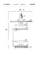
- FIG. 1shows a typical optical lithographic fabrication system 100 for delineating features in a workpiece 120.
- the workpiece 120comprises a semiconductor wafer (substrate), together with one or more layers of material(s) (not shown) located on a top major surface of the wafer.
- an optical source 106such as a mercury lamp
- the optical radiation emanating from the reticle 103is focused by the lens 102 onto a photoresist layer 101 located on the top major surface of the workpiece 120.
- the pattern of the reticle 103--that is, its pattern of transparent and opaque portions--is focused on the photoresist layer 101.
- this photoresisttypically a wet developer
- the material of the photoresistis removed or remains at and only at areas where the optical radiation was incident.
- the pattern of the maskis transferred to ("printed on") the photoresist layer 101.
- Subsequent etching processessuch as wet etching or dry plasma etching, remove selected portions of the workpiece 120.
- Portions of the workpiece 120thus are removed from the top surface of the workpiece 120 at areas underlying those where the photoresist layer 101 was removed by the development process but not at areas underlying those regions where the photoresist remains.
- impurity ionscan be implanted into the workpiece 120 at areas underlying those where the photoresist layer was removed by the development process but not at areas underlying where the photoresist remains.
- the pattern of the mask 103--i.e., each feature of the mask--is transferred to the workpiece 120 as is desired, for example, in the art of semiconductor integrated circuit fabrication.
- a transistor or other feature sizesuch as the feature size of a metallization stripe--i.e., its width--or of an aperture in an insulating layer which is to be filled with metal, in order to form electrical connections, for example, between one level of metallization and another.
- DOFdepth of focus
- the optical intensity transmission T of the opaque portions of the maskwas set at a value in the approximate range of 0.05 to 0.15 typically at approximately 0.10, rather than zero.
- the side lobes of the diffraction patternare undesirably increased in intensity, at the expense of the central lobe.
- OFF-axis illuminationimproves the DOF only for some values of, for example, the width L of a line feature printed on the PR layer, where a "line feature" refers to a feature in which its length is equal to at least three times its width L. More specifically, although OFF-axis illumination enhanced the DOF for cases in which L was equal to or less than approximately (0.75) ⁇ /(NA) and at the same time the spaces G between adjacent line features was also equal to or less than approximately (0.75) ⁇ /(NA), nevertheless OFF-axis illumination degraded both the DOF and the (dI/dx)/I of the image for cases in which L was equal to or greater than (0.75) ⁇ /(NA).
- This inventioninvolves an optical lithographic system in which an optical source directs optical radiation containing a wavelength ⁇ onto a patterned mask, to form an image feature on a photoresist layer located on the image plane of the system.
- the patterned maskhas an object feature in the form of the image feature, and the object feature has a portion whose width is everywhere less than or equal to ⁇ /NA, typically less than (0.5) ⁇ /NA, where NA is the numerical aperture of the image side of the system.
- An assist featurewhose width is everywhere less than (0.2) ⁇ /NA.
- the outside or the mask portion of the object feature(hereinafter “main feature”) is located on the mask in a neighborhood of the portion of the object feature, and has a distance of closest approach to the portion of the main object feature that is everywhere equal to less than (0.5) ⁇ /NA or else is located on the mask inside the portion of the main feature object.
- assistant featurerefers to a feature (pattern) located on the mask such that, when the mask is used as the reticle 103 in the system 100 (FIG.
- the image of the assist feature on the photoresist layer 101is sufficiently proximate to the image of the main feature thereon that the two images can be and is printed on the photoresist layer 101 as a single (merged) pattern--i.e., as though only a single (merged) image of the main and assist features had been formed.
- advantageously OFF-axis illuminationis used: for example, the optical radiation is directed successively through an annular aperture in an opaque screen and through a collimating lens onto the mask.
- proximity effectsthat is, the actual printed width of a feature of width L on the mask depends upon the distance G between neighboring object features on the mask.
- the use of the assist features of this inventionenables minimization of the proximity effects: that is, by using the invention the printed size of an object feature is less dependent on the presence of neighboring object features.
- FIGS. 1 and 2depict optical lithographic systems useful in the practice of this invention.
- FIGS. 3 through 6are top-view diagrams of portions of an optical mask, according to various embodiments of the invention.
- FIGURES.Only for the sake of clarity, none of the FIGURES. is drawn to any scale. In different FIGURES., elements that are the same, or are similar, are denoted by the same reference numerals.
- each of these masksis to be used in an optical lithographic system such as the previously described system 100 (FIG. 1) or the previously described system 200 (FIG. 2).
- a patterned optical lithographic maskhas a portion 30 indicated in FIG. 3.
- This portion 30comprises a group of parallel line segments, each representing a portion of a main feature (hereinafter, "main line segment") having a width L. Between adjacent line segments there exist mutually equal gap distances G, such that 1.0 ⁇ G/L ⁇ 1.5 and L ⁇ (0.5)(NA)/ ⁇ .
- Ggap distance
- Ggap distance
- the term “attenuation”will be used to describe situations in which T falls in the approximate range of 0.05 to 0.15 rather than T being equal to approximately 0.00 (“opaque”).
- a pair of assist features 31 and 32are located at the outside edges of the extreme left-hand and right-hand line segments (FIG. 3). Each of these assist features 31 and 32 has approximately the same transmission coefficient T as that of the line segments ("main features") themselves. Each of these assist features has a width s w equal to approximately (0.25) ⁇ /(NA) and is spaced apart from the nearest line segment by a distance s p that is equal to approximately (0.5) ⁇ /(NA). It should be recognized that this Example 1 is a case of "bright field" main features--i.e., dark main features that are situated on the mask in an environment of bright surroundings.
- each such assist feature 33is centrally located with respect to the end (hereinafter, "termination") of the main line segment and has a width that extends a distance equal to s p /2 to the left-hand and to the right-hand directions and that extends a distance equal to approximately s w in the direction parallel to the main line feature, where s p and s w are as defined before.
- each such assist feature 33is spaced from the termination of the main line feature by a distance equal to approximately s p , where s p is as defined above.
- Example 3the situation with respect to the main object features--i.e., the line segments (but not the assist features)--is the same as that described above in conjunction with FIG. 3 (and hence is the same as Example 1 or 2) except that in this Example 3 the ratio G/L satisfies: 1.5 ⁇ G/L ⁇ 3.0.
- Example 5the situation is the same as that described under Example 1 or 2 except that in this Example 5, L is approximately equal to ⁇ /(NA).
- an assist feature 46is inserted centrally inside each main line segment, rather than on the outside as in the above Examples 1, 2, 3, and 4.
- the quantities s p and s ware defined in terms of L, NA, and ⁇ in the same way as in Example 1. No assist feature is to be inserted outside the main line segment.
- Example 6the situation is the same as that described in Examples 1 or 2 except that in the situation of this Example 6,L ⁇ (1.5) ⁇ /(NA), and here no assist feature is required.
- a patterned optical lithographic mask(FIG. 5) has a portion 45.
- a square-shaped assist feature 42centrally located within the main feature 41, is added.
- This square-shaped assist feature 42has the form of a square, and it has an opposite transmission tone from that of the main square feature 41.
- advantageously ON-axis illuminationis used.
- a circular-shaped main feature having a diameter equal to 2Lcan be assisted by an assist feature whose diameter is approximately equal to s w , where L and s w are the same as defined above for the square-shaped main feature 41.
- a patterned optical lithographic maskhas a portion 50 indicated in FIG. 6.
- assist features 52are added each having a transmission tone that is the same as that of the main feature 51.
- either ON- or OFF-axis illuminationcan be used.
- OFF-axis illuminationis used in conjunction with a transmission coefficient T that falls in the approximate range between 0.05 and 0.15.
- Ttransmission coefficient
- all main features of the maskare isolated (i.e., are spaced apart by more than (1.5) ⁇ /(NA)) and are clear features (dark field) whose widths are less than approximately (0.75) ⁇ /(NA)
- the added advantage of OFF-axis illuminationis not significant.
- OFF-axis illumination without attenuation but with assist featuresresults in a significant improvement in the imaging process as opposed to omission of the assist features, but such an arrangement is not as good for imaging purposes as is OFF-axis illumination with attenuation except in the case described in the immediately preceding sentence.
Landscapes
- Physics & Mathematics (AREA)
- General Physics & Mathematics (AREA)
- Exposure And Positioning Against Photoresist Photosensitive Materials (AREA)
Abstract
Description
Claims (20)
Priority Applications (1)
| Application Number | Priority Date | Filing Date | Title |
|---|---|---|---|
| US08/550,879US5636002A (en) | 1994-04-29 | 1995-10-31 | Auxiliary mask features for enhancing the resolution of photolithography |
Applications Claiming Priority (2)
| Application Number | Priority Date | Filing Date | Title |
|---|---|---|---|
| US23572194A | 1994-04-29 | 1994-04-29 | |
| US08/550,879US5636002A (en) | 1994-04-29 | 1995-10-31 | Auxiliary mask features for enhancing the resolution of photolithography |
Related Parent Applications (1)
| Application Number | Title | Priority Date | Filing Date |
|---|---|---|---|
| US23572194AContinuation-In-Part | 1994-04-29 | 1994-04-29 |
Publications (1)
| Publication Number | Publication Date |
|---|---|
| US5636002Atrue US5636002A (en) | 1997-06-03 |
Family
ID=22886660
Family Applications (1)
| Application Number | Title | Priority Date | Filing Date |
|---|---|---|---|
| US08/550,879Expired - LifetimeUS5636002A (en) | 1994-04-29 | 1995-10-31 | Auxiliary mask features for enhancing the resolution of photolithography |
Country Status (1)
| Country | Link |
|---|---|
| US (1) | US5636002A (en) |
Cited By (58)
| Publication number | Priority date | Publication date | Assignee | Title |
|---|---|---|---|---|
| US5900340A (en)* | 1997-03-03 | 1999-05-04 | Motorola, Inc. | One dimensional lithographic proximity correction using DRC shape functions |
| US6011611A (en)* | 1997-11-07 | 2000-01-04 | Kabushiki Kaisha Toshiba | Method of measuring aberration of projection optics |
| US6021009A (en)* | 1998-06-30 | 2000-02-01 | Intel Corporation | Method and apparatus to improve across field dimensional control in a microlithography tool |
| US6165693A (en)* | 1998-06-11 | 2000-12-26 | United Microelectronics Corp. | Method of designing an assist feature |
| US6214497B1 (en) | 1999-06-29 | 2001-04-10 | Micron Technology, Inc. | Method to eliminate side lobe printing of attenuated phase shift masks |
| US6258490B1 (en) | 1999-07-09 | 2001-07-10 | International Business Machines Corporation | Transmission control mask utilized to reduce foreshortening effects |
| US6401236B1 (en) | 1999-04-05 | 2002-06-04 | Micron Technology Inc. | Method to eliminate side lobe printing of attenuated phase shift |
| US6453457B1 (en) | 2000-09-29 | 2002-09-17 | Numerical Technologies, Inc. | Selection of evaluation point locations based on proximity effects model amplitudes for correcting proximity effects in a fabrication layout |
| US20020199157A1 (en)* | 1999-04-30 | 2002-12-26 | Cobb Nicolas Bailey | Mixed-mode optical proximity correction |
| US6514648B2 (en) | 1998-08-28 | 2003-02-04 | International Business Machines Corporation | Method to produce equal sized features in microlithography |
| US6523162B1 (en) | 2000-08-02 | 2003-02-18 | Numerical Technologies, Inc. | General purpose shape-based layout processing scheme for IC layout modifications |
| US6541165B1 (en) | 2000-07-05 | 2003-04-01 | Numerical Technologies, Inc. | Phase shift mask sub-resolution assist features |
| US6553559B2 (en) | 2001-01-05 | 2003-04-22 | International Business Machines Corporation | Method to determine optical proximity correction and assist feature rules which account for variations in mask dimensions |
| US20030097647A1 (en)* | 2000-02-28 | 2003-05-22 | Numerical Technologies, Inc. | Method and apparatus for mixed-mode optical proximity correction |
| US20030117605A1 (en)* | 2001-12-20 | 2003-06-26 | Nanya Technology Corporation | Apparatus and method for contact hole exposure |
| US6602728B1 (en) | 2001-01-05 | 2003-08-05 | International Business Machines Corporation | Method for generating a proximity model based on proximity rules |
| US6625801B1 (en) | 2000-09-29 | 2003-09-23 | Numerical Technologies, Inc. | Dissection of printed edges from a fabrication layout for correcting proximity effects |
| US6653026B2 (en) | 2000-12-20 | 2003-11-25 | Numerical Technologies, Inc. | Structure and method of correcting proximity effects in a tri-tone attenuated phase-shifting mask |
| US6653028B2 (en)* | 2000-05-31 | 2003-11-25 | Boe-Hydis Technology Co., Ltd. | Photo mask for fabricating a thin film transistor liquid crystal display |
| US6665856B1 (en) | 2000-12-01 | 2003-12-16 | Numerical Technologies, Inc. | Displacing edge segments on a fabrication layout based on proximity effects model amplitudes for correcting proximity effects |
| US6670082B2 (en) | 2001-10-09 | 2003-12-30 | Numerical Technologies, Inc. | System and method for correcting 3D effects in an alternating phase-shifting mask |
| US6684382B2 (en) | 2001-08-31 | 2004-01-27 | Numerical Technologies, Inc. | Microloading effect correction |
| US20040063000A1 (en)* | 2002-09-27 | 2004-04-01 | Mentor Graphics Corporation | Chromeless phase mask layout generation |
| US20040138860A1 (en)* | 2003-01-13 | 2004-07-15 | Stanton William A. | Methods of forming radiation-patterning tools; carrier waves and computer readable media |
| US6777141B2 (en) | 2000-07-05 | 2004-08-17 | Numerical Technologies, Inc. | Phase shift mask including sub-resolution assist features for isolated spaces |
| US20040172610A1 (en)* | 2003-02-28 | 2004-09-02 | International Business Machines Corporation | Pitch-based subresolution assist feature design |
| US6792590B1 (en) | 2000-09-29 | 2004-09-14 | Numerical Technologies, Inc. | Dissection of edges with projection points in a fabrication layout for correcting proximity effects |
| US20040188383A1 (en)* | 2003-03-27 | 2004-09-30 | Lucas Kevin D. | Non-resolving mask tiling method for flare reduction |
| US20050026047A1 (en)* | 2003-08-01 | 2005-02-03 | Yang Chin Cheng | Mask for reducing proximity effect |
| US20050096888A1 (en)* | 2001-05-11 | 2005-05-05 | Ismail Yehea I. | Efficient model order reduction via multi-point moment matching |
| US6900124B1 (en) | 2003-09-03 | 2005-05-31 | Advanced Micro Devices, Inc. | Patterning for elliptical Vss contact on flash memory |
| US20060292885A1 (en)* | 2005-06-24 | 2006-12-28 | Texas Instruments Incorporated | Layout modification to eliminate line bending caused by line material shrinkage |
| US20100252890A1 (en)* | 2008-03-13 | 2010-10-07 | Tela Innovations, Inc. | Linear Gate Level Cross-Coupled Transistor Device with Non-Overlapping PMOS Transistors and Non-Overlapping NMOS Transistors Relative to Direction of Gate Electrodes |
| US8089101B2 (en) | 2006-03-09 | 2012-01-03 | Tela Innovations, Inc. | Integrated circuit device with gate electrode level region including two side-by-side ones of at least three linear-shaped conductive structures electrically connected to each other through non-gate level |
| US8214778B2 (en) | 2007-08-02 | 2012-07-03 | Tela Innovations, Inc. | Methods for cell phasing and placement in dynamic array architecture and implementation of the same |
| US8225239B2 (en)* | 2006-03-09 | 2012-07-17 | Tela Innovations, Inc. | Methods for defining and utilizing sub-resolution features in linear topology |
| US8225261B2 (en) | 2006-03-09 | 2012-07-17 | Tela Innovations, Inc. | Methods for defining contact grid in dynamic array architecture |
| US8245180B2 (en) | 2006-03-09 | 2012-08-14 | Tela Innovations, Inc. | Methods for defining and using co-optimized nanopatterns for integrated circuit design and apparatus implementing same |
| US8247846B2 (en) | 2006-03-09 | 2012-08-21 | Tela Innovations, Inc. | Oversized contacts and vias in semiconductor chip defined by linearly constrained topology |
| US8286107B2 (en) | 2007-02-20 | 2012-10-09 | Tela Innovations, Inc. | Methods and systems for process compensation technique acceleration |
| US8283701B2 (en) | 2007-08-02 | 2012-10-09 | Tela Innovations, Inc. | Semiconductor device with dynamic array sections defined and placed according to manufacturing assurance halos |
| US8448102B2 (en) | 2006-03-09 | 2013-05-21 | Tela Innovations, Inc. | Optimizing layout of irregular structures in regular layout context |
| US8453094B2 (en) | 2008-01-31 | 2013-05-28 | Tela Innovations, Inc. | Enforcement of semiconductor structure regularity for localized transistors and interconnect |
| US8471391B2 (en) | 2008-03-27 | 2013-06-25 | Tela Innovations, Inc. | Methods for multi-wire routing and apparatus implementing same |
| US8541879B2 (en) | 2007-12-13 | 2013-09-24 | Tela Innovations, Inc. | Super-self-aligned contacts and method for making the same |
| US8653857B2 (en) | 2006-03-09 | 2014-02-18 | Tela Innovations, Inc. | Circuitry and layouts for XOR and XNOR logic |
| US8658542B2 (en) | 2006-03-09 | 2014-02-25 | Tela Innovations, Inc. | Coarse grid design methods and structures |
| US8661392B2 (en) | 2009-10-13 | 2014-02-25 | Tela Innovations, Inc. | Methods for cell boundary encroachment and layouts implementing the Same |
| US8667443B2 (en) | 2007-03-05 | 2014-03-04 | Tela Innovations, Inc. | Integrated circuit cell library for multiple patterning |
| US8680626B2 (en) | 2007-10-26 | 2014-03-25 | Tela Innovations, Inc. | Methods, structures, and designs for self-aligning local interconnects used in integrated circuits |
| US8839175B2 (en) | 2006-03-09 | 2014-09-16 | Tela Innovations, Inc. | Scalable meta-data objects |
| US8863063B2 (en) | 2009-05-06 | 2014-10-14 | Tela Innovations, Inc. | Finfet transistor circuit |
| US9035359B2 (en) | 2006-03-09 | 2015-05-19 | Tela Innovations, Inc. | Semiconductor chip including region including linear-shaped conductive structures forming gate electrodes and having electrical connection areas arranged relative to inner region between transistors of different types and associated methods |
| US9122832B2 (en) | 2008-08-01 | 2015-09-01 | Tela Innovations, Inc. | Methods for controlling microloading variation in semiconductor wafer layout and fabrication |
| US9159627B2 (en) | 2010-11-12 | 2015-10-13 | Tela Innovations, Inc. | Methods for linewidth modification and apparatus implementing the same |
| US9230910B2 (en) | 2006-03-09 | 2016-01-05 | Tela Innovations, Inc. | Oversized contacts and vias in layout defined by linearly constrained topology |
| US9563733B2 (en) | 2009-05-06 | 2017-02-07 | Tela Innovations, Inc. | Cell circuit and layout with linear finfet structures |
| CN115524917A (en)* | 2021-08-30 | 2022-12-27 | 台湾积体电路制造股份有限公司 | Photomask and method of manufacturing semiconductor device |
Citations (5)
| Publication number | Priority date | Publication date | Assignee | Title |
|---|---|---|---|---|
| US5117254A (en)* | 1988-05-13 | 1992-05-26 | Canon Kabushiki Kaisha | Projection exposure apparatus |
| US5184196A (en)* | 1990-12-26 | 1993-02-02 | Nikon Corporation | Projection exposure apparatus |
| US5286581A (en)* | 1991-08-19 | 1994-02-15 | Motorola, Inc. | Phase-shift mask and method for making |
| US5300971A (en)* | 1992-02-17 | 1994-04-05 | Nikon Corporation | Projection exposure apparatus |
| US5357311A (en)* | 1991-02-25 | 1994-10-18 | Nikon Corporation | Projection type light exposure apparatus and light exposure method |
- 1995
- 1995-10-31USUS08/550,879patent/US5636002A/ennot_activeExpired - Lifetime
Patent Citations (5)
| Publication number | Priority date | Publication date | Assignee | Title |
|---|---|---|---|---|
| US5117254A (en)* | 1988-05-13 | 1992-05-26 | Canon Kabushiki Kaisha | Projection exposure apparatus |
| US5184196A (en)* | 1990-12-26 | 1993-02-02 | Nikon Corporation | Projection exposure apparatus |
| US5357311A (en)* | 1991-02-25 | 1994-10-18 | Nikon Corporation | Projection type light exposure apparatus and light exposure method |
| US5286581A (en)* | 1991-08-19 | 1994-02-15 | Motorola, Inc. | Phase-shift mask and method for making |
| US5300971A (en)* | 1992-02-17 | 1994-04-05 | Nikon Corporation | Projection exposure apparatus |
Cited By (227)
| Publication number | Priority date | Publication date | Assignee | Title |
|---|---|---|---|---|
| US5900340A (en)* | 1997-03-03 | 1999-05-04 | Motorola, Inc. | One dimensional lithographic proximity correction using DRC shape functions |
| US6011611A (en)* | 1997-11-07 | 2000-01-04 | Kabushiki Kaisha Toshiba | Method of measuring aberration of projection optics |
| US6165693A (en)* | 1998-06-11 | 2000-12-26 | United Microelectronics Corp. | Method of designing an assist feature |
| US6021009A (en)* | 1998-06-30 | 2000-02-01 | Intel Corporation | Method and apparatus to improve across field dimensional control in a microlithography tool |
| US6514648B2 (en) | 1998-08-28 | 2003-02-04 | International Business Machines Corporation | Method to produce equal sized features in microlithography |
| US6517978B2 (en) | 1998-08-28 | 2003-02-11 | International Business Machines Corporation | Method to produce equal sized features in microlithography |
| US6401236B1 (en) | 1999-04-05 | 2002-06-04 | Micron Technology Inc. | Method to eliminate side lobe printing of attenuated phase shift |
| US7024655B2 (en) | 1999-04-30 | 2006-04-04 | Cobb Nicolas B | Mixed-mode optical proximity correction |
| US20020199157A1 (en)* | 1999-04-30 | 2002-12-26 | Cobb Nicolas Bailey | Mixed-mode optical proximity correction |
| US20040221254A1 (en)* | 1999-04-30 | 2004-11-04 | Mentor Graphics Corporation | Mixed mode optical proximity correction |
| US6413684B1 (en) | 1999-06-29 | 2002-07-02 | Micron Technology, Inc. | Method to eliminate side lobe printing of attenuated phase shift masks |
| US6214497B1 (en) | 1999-06-29 | 2001-04-10 | Micron Technology, Inc. | Method to eliminate side lobe printing of attenuated phase shift masks |
| US6258490B1 (en) | 1999-07-09 | 2001-07-10 | International Business Machines Corporation | Transmission control mask utilized to reduce foreshortening effects |
| US20030097647A1 (en)* | 2000-02-28 | 2003-05-22 | Numerical Technologies, Inc. | Method and apparatus for mixed-mode optical proximity correction |
| US6584609B1 (en) | 2000-02-28 | 2003-06-24 | Numerical Technologies, Inc. | Method and apparatus for mixed-mode optical proximity correction |
| US6988259B2 (en) | 2000-02-28 | 2006-01-17 | Synopsys, Inc. | Method and apparatus for mixed-mode optical proximity correction |
| US6653028B2 (en)* | 2000-05-31 | 2003-11-25 | Boe-Hydis Technology Co., Ltd. | Photo mask for fabricating a thin film transistor liquid crystal display |
| US6541165B1 (en) | 2000-07-05 | 2003-04-01 | Numerical Technologies, Inc. | Phase shift mask sub-resolution assist features |
| US7585595B2 (en) | 2000-07-05 | 2009-09-08 | Synopsys, Inc. | Phase shift mask including sub-resolution assist features for isolated spaces |
| US6777141B2 (en) | 2000-07-05 | 2004-08-17 | Numerical Technologies, Inc. | Phase shift mask including sub-resolution assist features for isolated spaces |
| US6523162B1 (en) | 2000-08-02 | 2003-02-18 | Numerical Technologies, Inc. | General purpose shape-based layout processing scheme for IC layout modifications |
| US7003757B2 (en) | 2000-09-29 | 2006-02-21 | Synopsys, Inc. | Dissection of edges with projection points in a fabrication layout for correcting proximity effects |
| US6625801B1 (en) | 2000-09-29 | 2003-09-23 | Numerical Technologies, Inc. | Dissection of printed edges from a fabrication layout for correcting proximity effects |
| US6918104B2 (en) | 2000-09-29 | 2005-07-12 | Synopsys, Inc. | Dissection of printed edges from a fabrication layout for correcting proximity effects |
| US6453457B1 (en) | 2000-09-29 | 2002-09-17 | Numerical Technologies, Inc. | Selection of evaluation point locations based on proximity effects model amplitudes for correcting proximity effects in a fabrication layout |
| US20040221255A1 (en)* | 2000-09-29 | 2004-11-04 | Numerical Technologies, Inc. | Dissection of edges with projection points in a fabrication layout for correcting proximity effects |
| US6792590B1 (en) | 2000-09-29 | 2004-09-14 | Numerical Technologies, Inc. | Dissection of edges with projection points in a fabrication layout for correcting proximity effects |
| US20040083439A1 (en)* | 2000-12-01 | 2004-04-29 | Numerical Technologies, Inc. | Displacing edge segments on a fabrication layout based on proximity effects model amplitudes for correcting proximity effects |
| US7926004B2 (en) | 2000-12-01 | 2011-04-12 | Synopsys, Inc. | Displacing edge segments on a fabrication layout based on proximity effects model amplitudes for correcting proximity effects |
| US20090249266A1 (en)* | 2000-12-01 | 2009-10-01 | Synopsys, Inc. | Displacing Edge Segments On A Fabrication Layout Based On Proximity Effects Model Amplitudes For Correcting Proximity Effects |
| US7562319B2 (en) | 2000-12-01 | 2009-07-14 | Synopsys, Inc. | Displacing edge segments on a fabrication layout based on proximity effects model amplitudes for correcting proximity effects |
| US20070006118A1 (en)* | 2000-12-01 | 2007-01-04 | Synopsys Inc. | Displacing Edge Segments On A Fabrication Layout Based On Proximity Effects Model Amplitudes For Correcting Proximity Effects |
| US7131101B2 (en) | 2000-12-01 | 2006-10-31 | Synopsys Inc. | Displacing edge segments on a fabrication layout based on proximity effects model amplitudes for correcting proximity effects |
| US6665856B1 (en) | 2000-12-01 | 2003-12-16 | Numerical Technologies, Inc. | Displacing edge segments on a fabrication layout based on proximity effects model amplitudes for correcting proximity effects |
| US7236916B2 (en) | 2000-12-20 | 2007-06-26 | Synopsys, Inc. | Structure and method of correcting proximity effects in a tri-tone attenuated phase-shifting mask |
| US6653026B2 (en) | 2000-12-20 | 2003-11-25 | Numerical Technologies, Inc. | Structure and method of correcting proximity effects in a tri-tone attenuated phase-shifting mask |
| US6553559B2 (en) | 2001-01-05 | 2003-04-22 | International Business Machines Corporation | Method to determine optical proximity correction and assist feature rules which account for variations in mask dimensions |
| US6602728B1 (en) | 2001-01-05 | 2003-08-05 | International Business Machines Corporation | Method for generating a proximity model based on proximity rules |
| US20050096888A1 (en)* | 2001-05-11 | 2005-05-05 | Ismail Yehea I. | Efficient model order reduction via multi-point moment matching |
| US6684382B2 (en) | 2001-08-31 | 2004-01-27 | Numerical Technologies, Inc. | Microloading effect correction |
| US6830854B2 (en) | 2001-10-09 | 2004-12-14 | Numerical Technologies, Inc. | System and method for correcting 3D effects in an alternating phase-shifting mask |
| US6670082B2 (en) | 2001-10-09 | 2003-12-30 | Numerical Technologies, Inc. | System and method for correcting 3D effects in an alternating phase-shifting mask |
| US20040076895A1 (en)* | 2001-10-09 | 2004-04-22 | Numerical Technologies, Inc. | System and method for correcting 3D effects in an alternating phase-shifting mask |
| US20030117605A1 (en)* | 2001-12-20 | 2003-06-26 | Nanya Technology Corporation | Apparatus and method for contact hole exposure |
| US7172838B2 (en) | 2002-09-27 | 2007-02-06 | Wilhelm Maurer | Chromeless phase mask layout generation |
| US20040063000A1 (en)* | 2002-09-27 | 2004-04-01 | Mentor Graphics Corporation | Chromeless phase mask layout generation |
| US20050049839A1 (en)* | 2003-01-13 | 2005-03-03 | Stanton William A. | Methods of forming radiation-patterning tools; carrier waves and computer readable media |
| US20040138860A1 (en)* | 2003-01-13 | 2004-07-15 | Stanton William A. | Methods of forming radiation-patterning tools; carrier waves and computer readable media |
| US6807519B2 (en)* | 2003-01-13 | 2004-10-19 | Micron Technology, Inc. | Methods of forming radiation-patterning tools; carrier waves and computer readable media |
| US7401010B2 (en) | 2003-01-13 | 2008-07-15 | Micron Technology, Inc. | Methods of forming radiation-patterning tools; carrier waves and computer readable media |
| US6964032B2 (en) | 2003-02-28 | 2005-11-08 | International Business Machines Corporation | Pitch-based subresolution assist feature design |
| US20040172610A1 (en)* | 2003-02-28 | 2004-09-02 | International Business Machines Corporation | Pitch-based subresolution assist feature design |
| US6989229B2 (en)* | 2003-03-27 | 2006-01-24 | Freescale Semiconductor, Inc. | Non-resolving mask tiling method for flare reduction |
| US20040188383A1 (en)* | 2003-03-27 | 2004-09-30 | Lucas Kevin D. | Non-resolving mask tiling method for flare reduction |
| US20050026047A1 (en)* | 2003-08-01 | 2005-02-03 | Yang Chin Cheng | Mask for reducing proximity effect |
| US6983444B2 (en)* | 2003-08-01 | 2006-01-03 | Macronix International Co., Ltd. | Mask for reducing proximity effect |
| US7018922B1 (en) | 2003-09-03 | 2006-03-28 | Advanced Micro Devices, Inc. | Patterning for elongated VSS contact flash memory |
| US6900124B1 (en) | 2003-09-03 | 2005-05-31 | Advanced Micro Devices, Inc. | Patterning for elliptical Vss contact on flash memory |
| US20060292885A1 (en)* | 2005-06-24 | 2006-12-28 | Texas Instruments Incorporated | Layout modification to eliminate line bending caused by line material shrinkage |
| US8952425B2 (en) | 2006-03-09 | 2015-02-10 | Tela Innovations, Inc. | Integrated circuit including at least four linear-shaped conductive structures having extending portions of different length |
| US8258550B2 (en) | 2006-03-09 | 2012-09-04 | Tela Innovations, Inc. | Semiconductor device including at least six transistor forming linear shapes including at least two transistor forming linear shapes having different extension distances beyond gate contact |
| US8089099B2 (en) | 2006-03-09 | 2012-01-03 | Tela Innovations, Inc, | Integrated circuit device and associated layout including gate electrode level region of 965 NM radius with linear-shaped conductive segments on fixed pitch |
| US8089098B2 (en) | 2006-03-09 | 2012-01-03 | Tela Innovations, Inc. | Integrated circuit device and associated layout including linear gate electrodes of different transistor types next to linear-shaped non-gate conductive segment |
| US8089102B2 (en) | 2006-03-09 | 2012-01-03 | Tela Innovations, Inc. | Method for fabricating integrated circuit having three or more linear-shaped gate electrode level conductive segments of both equal length and equal pitch |
| US8088682B2 (en) | 2006-03-09 | 2012-01-03 | Tela Innovations, Inc. | Method for fabricating integrated circuit with gate electrode level region including two side-by-side ones of at least three linear-shaped conductive structures electrically connected to each other through non-gate level |
| US8089103B2 (en) | 2006-03-09 | 2012-01-03 | Tela Innovations, Inc. | Integrated circuit device with gate level region including at least three linear-shaped conductive segments having offset line ends and forming three transistors of first type and one transistor of second type |
| US8088681B2 (en) | 2006-03-09 | 2012-01-03 | Tela Innovations, Inc. | Method for fabricating integrated circuit including separated diffusion regions of different type each having four gate electrodes with each of two complementary gate electrode pairs formed from respective linear condcutive segment |
| US8088679B2 (en) | 2006-03-09 | 2012-01-03 | Tela Innovations, Inc. | Method for fabricating integrated circuit with gate electrode level portion including at least two complementary transistor forming linear conductive segments and at least one non-gate linear conductive segment |
| US8089100B2 (en) | 2006-03-09 | 2012-01-03 | Tela Innovations, Inc. | Integrated circuit with gate electrode level region including at least four linear-shaped conductive structures forming gate electrodes of transistors and including extending portions of at least two different sizes |
| US8088680B2 (en) | 2006-03-09 | 2012-01-03 | Tela Innovations, Inc. | Method for fabricating integrated circuit having at least three linear-shaped gate electrode level conductive features of equal length positioned side-by-side at equal pitch |
| US8089104B2 (en) | 2006-03-09 | 2012-01-03 | Tela Innovations, Inc. | Integrated circuit with gate electrode level region including multiple linear-shaped conductive structures forming gate electrodes of transistors and including uniformity extending portions of different size |
| US8101975B2 (en) | 2006-03-09 | 2012-01-24 | Tela Innovations, Inc. | Integrated circuit device with gate level region including non-gate linear conductive segment positioned within 965 nanometers of four transistors of first type and four transistors of second type |
| US8110854B2 (en) | 2006-03-09 | 2012-02-07 | Tela Innovations, Inc. | Integrated circuit device with linearly defined gate electrode level region and shared diffusion region of first type connected to shared diffusion region of second type through at least two interconnect levels |
| US8129753B2 (en) | 2006-03-09 | 2012-03-06 | Tela Innovations, Inc. | Integrated circuit including gate electrode level region including at least seven linear-shaped conductive structures of equal length positioned at equal pitch with at least two linear-shaped conductive structures each forming one transistor and having extending portion sized greater than gate portion |
| US8129757B2 (en) | 2006-03-09 | 2012-03-06 | Tela Innovations, Inc. | Integrated circuit including at least six linear-shaped conductive structive structures at equal pitch including at least two linear-shaped conductive structures having non-gate portions of different length |
| US8129750B2 (en) | 2006-03-09 | 2012-03-06 | Tela Innovations, Inc. | Integrated circuit including at least six linear-shaped conductive structures forming gate electrodes of transistors with at least two linear-shaped conductive structures of different length |
| US8129754B2 (en) | 2006-03-09 | 2012-03-06 | Tela Innovations, Inc. | Integrated circuit with gate electrode level including at least six linear-shaped conductive structures forming gate electrodes of transisters with at least one pair of linear-shaped conductive structures having offset ends |
| US8129751B2 (en) | 2006-03-09 | 2012-03-06 | Tela Innovations, Inc. | Integrated circuit including at least six linear-shaped conductive structures forming gate electrodes and including four conductive contacting structures having at least two different connection distances |
| US8129752B2 (en) | 2006-03-09 | 2012-03-06 | Tela Innovations, Inc. | Integrated circuit including a linear-shaped conductive structure forming one gate electrode and having length greater than or equal to one-half the length of linear-shaped conductive structure forming two gate electrodes |
| US8129756B2 (en) | 2006-03-09 | 2012-03-06 | Tela Innovations, Inc. | Integrated circuit including at least six linear-shaped conductive structures forming gate electrodes of transistors with at least two different extension distances beyond conductive contacting structures |
| US8129755B2 (en) | 2006-03-09 | 2012-03-06 | Tela Innovations, Inc. | Integrated circuit with gate electrode level including at least four linear-shaped conductive structures of equal length and equal pitch with linear-shaped conductive structure forming one transistor |
| US8129819B2 (en) | 2006-03-09 | 2012-03-06 | Tela Innovations, Inc. | Method of fabricating integrated circuit including at least six linear-shaped conductive structures at equal pitch including at least two linear-shaped conductive structures having non-gate portions of different length |
| US8134186B2 (en) | 2006-03-09 | 2012-03-13 | Tela Innovations, Inc. | Integrated circuit including at least three linear-shaped conductive structures at equal pitch including linear-shaped conductive structure having non-gate portion length greater than gate portion length |
| US8134184B2 (en) | 2006-03-09 | 2012-03-13 | Tela Innovations, Inc. | Integrated circuit having gate electrode level region including at least four linear-shaped conductive structures with some outer-contacted linear-shaped conductive structures having larger outer extending portion than inner extending portion |
| US8134183B2 (en) | 2006-03-09 | 2012-03-13 | Tela Innovations, Inc. | Integrated circuit including linear-shaped conductive structures that have gate portions and extending portions of different size |
| US8134185B2 (en) | 2006-03-09 | 2012-03-13 | Tela Innovations, Inc. | Integrated circuit having gate electrode level region including at least seven linear-shaped conductive structures at equal pitch including linear-shaped conductive structure forming transistors of two different types and at least three linear-shaped conductive structures having aligned ends |
| US8138525B2 (en) | 2006-03-09 | 2012-03-20 | Tela Innovations, Inc. | Integrated circuit including at least three linear-shaped conductive structures of different length each forming gate of different transistor |
| US8198656B2 (en) | 2006-03-09 | 2012-06-12 | Tela Innovations, Inc. | Integrated circuit including gate electrode level region including at least four linear-shaped conductive structures of equal length having aligned ends and positioned at equal pitch and forming multiple gate electrodes of transistors of different type |
| US8207053B2 (en) | 2006-03-09 | 2012-06-26 | Tela Innovations, Inc. | Electrodes of transistors with at least two linear-shaped conductive structures of different length |
| US8921897B2 (en) | 2006-03-09 | 2014-12-30 | Tela Innovations, Inc. | Integrated circuit with gate electrode conductive structures having offset ends |
| US8217428B2 (en) | 2006-03-09 | 2012-07-10 | Tela Innovations, Inc. | Integrated circuit including gate electrode level region including at least three linear-shaped conductive structures of equal length having aligned ends and positioned at equal pitch and forming multiple gate electrodes of transistors of different type |
| US8225239B2 (en)* | 2006-03-09 | 2012-07-17 | Tela Innovations, Inc. | Methods for defining and utilizing sub-resolution features in linear topology |
| US8225261B2 (en) | 2006-03-09 | 2012-07-17 | Tela Innovations, Inc. | Methods for defining contact grid in dynamic array architecture |
| US8245180B2 (en) | 2006-03-09 | 2012-08-14 | Tela Innovations, Inc. | Methods for defining and using co-optimized nanopatterns for integrated circuit design and apparatus implementing same |
| US8247846B2 (en) | 2006-03-09 | 2012-08-21 | Tela Innovations, Inc. | Oversized contacts and vias in semiconductor chip defined by linearly constrained topology |
| US8253172B2 (en) | 2006-03-09 | 2012-08-28 | Tela Innovations, Inc. | Semiconductor device with linearly restricted gate level region including four serially connected transistors of first type and four serially connected transistors of second type separated by non-diffusion region |
| US8253173B2 (en) | 2006-03-09 | 2012-08-28 | Tela Innovations, Inc. | Semiconductor device with gate level including four transistors of first type and four transistors of second type separated by non-diffusion region and having at least two gate contacts positioned outside separating non-diffusion region |
| US8946781B2 (en) | 2006-03-09 | 2015-02-03 | Tela Innovations, Inc. | Integrated circuit including gate electrode conductive structures with different extension distances beyond contact |
| US9589091B2 (en) | 2006-03-09 | 2017-03-07 | Tela Innovations, Inc. | Scalable meta-data objects |
| US8258551B2 (en) | 2006-03-09 | 2012-09-04 | Tela Innovations, Inc. | Semiconductor device with gate level including transistors of first type and transistors of second type with corresponding gate contact placement restriction |
| US8258547B2 (en) | 2006-03-09 | 2012-09-04 | Tela Innovations, Inc. | Semiconductor device with linearly restricted gate level region including two transistors of first type and two transistors of second type with offset gate contacts |
| US8258552B2 (en) | 2006-03-09 | 2012-09-04 | Tela Innovations, Inc. | Semiconductor device including at least six transistor forming linear shapes with at least two transistor forming linear shapes having offset ends |
| US8258549B2 (en) | 2006-03-09 | 2012-09-04 | Tela Innovations, Inc. | Semiconductor device including two transistors of first type having gates formed by conductors of different length respectively aligned with two transistors of second type having gates formed by conductors of different length |
| US8258548B2 (en) | 2006-03-09 | 2012-09-04 | Tela Innovations, Inc. | Semiconductor device with gate level including four transistors of first type and four transistors of second type separated by non-diffusion region with restricted gate contact placement over separating non-diffusion region |
| US8264008B2 (en) | 2006-03-09 | 2012-09-11 | Tela Innovations, Inc. | Semiconductor device including transistor forming linear shapes including gate portions and extending portions of different size |
| US9009641B2 (en) | 2006-03-09 | 2015-04-14 | Tela Innovations, Inc. | Circuits with linear finfet structures |
| US8264007B2 (en) | 2006-03-09 | 2012-09-11 | Tela Innovations, Inc. | Semiconductor device including at least six transistor forming linear shapes including at least two different gate contact connection distances |
| US8264009B2 (en) | 2006-03-09 | 2012-09-11 | Tela Innovations, Inc. | Semiconductor device with linearly restricted gate level region including four transistors of first type and four transistors of second type with gate defining shapes of different length |
| US10230377B2 (en) | 2006-03-09 | 2019-03-12 | Tela Innovations, Inc. | Circuitry and layouts for XOR and XNOR logic |
| US10217763B2 (en) | 2006-03-09 | 2019-02-26 | Tela Innovations, Inc. | Semiconductor chip having region including gate electrode features of rectangular shape on gate horizontal grid and first-metal structures of rectangular shape on at least eight first-metal gridlines of first-metal vertical grid |
| US8921896B2 (en) | 2006-03-09 | 2014-12-30 | Tela Innovations, Inc. | Integrated circuit including linear gate electrode structures having different extension distances beyond contact |
| US8839175B2 (en) | 2006-03-09 | 2014-09-16 | Tela Innovations, Inc. | Scalable meta-data objects |
| US8823062B2 (en) | 2006-03-09 | 2014-09-02 | Tela Innovations, Inc. | Integrated circuit with offset line end spacings in linear gate electrode level |
| US10186523B2 (en) | 2006-03-09 | 2019-01-22 | Tela Innovations, Inc. | Semiconductor chip having region including gate electrode features formed in part from rectangular layout shapes on gate horizontal grid and first-metal structures formed in part from rectangular layout shapes on at least eight first-metal gridlines of first-metal vertical grid |
| US10141335B2 (en) | 2006-03-09 | 2018-11-27 | Tela Innovations, Inc. | Semiconductor CIP including region having rectangular-shaped gate structures and first metal structures |
| US10141334B2 (en) | 2006-03-09 | 2018-11-27 | Tela Innovations, Inc. | Semiconductor chip including region having rectangular-shaped gate structures and first-metal structures |
| US8436400B2 (en) | 2006-03-09 | 2013-05-07 | Tela Innovations, Inc. | Semiconductor device with gate level including gate electrode conductors for transistors of first type and transistors of second type with some gate electrode conductors of different length |
| US8448102B2 (en) | 2006-03-09 | 2013-05-21 | Tela Innovations, Inc. | Optimizing layout of irregular structures in regular layout context |
| US9035359B2 (en) | 2006-03-09 | 2015-05-19 | Tela Innovations, Inc. | Semiconductor chip including region including linear-shaped conductive structures forming gate electrodes and having electrical connection areas arranged relative to inner region between transistors of different types and associated methods |
| US9230910B2 (en) | 2006-03-09 | 2016-01-05 | Tela Innovations, Inc. | Oversized contacts and vias in layout defined by linearly constrained topology |
| US9240413B2 (en) | 2006-03-09 | 2016-01-19 | Tela Innovations, Inc. | Methods, structures, and designs for self-aligning local interconnects used in integrated circuits |
| US9336344B2 (en) | 2006-03-09 | 2016-05-10 | Tela Innovations, Inc. | Coarse grid design methods and structures |
| US9917056B2 (en) | 2006-03-09 | 2018-03-13 | Tela Innovations, Inc. | Coarse grid design methods and structures |
| US9425145B2 (en) | 2006-03-09 | 2016-08-23 | Tela Innovations, Inc. | Oversized contacts and vias in layout defined by linearly constrained topology |
| US9905576B2 (en) | 2006-03-09 | 2018-02-27 | Tela Innovations, Inc. | Semiconductor chip including region having rectangular-shaped gate structures and first metal structures |
| US9859277B2 (en) | 2006-03-09 | 2018-01-02 | Tela Innovations, Inc. | Methods, structures, and designs for self-aligning local interconnects used in integrated circuits |
| US9425272B2 (en) | 2006-03-09 | 2016-08-23 | Tela Innovations, Inc. | Semiconductor chip including integrated circuit including four transistors of first transistor type and four transistors of second transistor type with electrical connections between various transistors and methods for manufacturing the same |
| US9754878B2 (en) | 2006-03-09 | 2017-09-05 | Tela Innovations, Inc. | Semiconductor chip including a chip level based on a layout that includes both regular and irregular wires |
| US9741719B2 (en) | 2006-03-09 | 2017-08-22 | Tela Innovations, Inc. | Methods, structures, and designs for self-aligning local interconnects used in integrated circuits |
| US9711495B2 (en) | 2006-03-09 | 2017-07-18 | Tela Innovations, Inc. | Oversized contacts and vias in layout defined by linearly constrained topology |
| US9673825B2 (en) | 2006-03-09 | 2017-06-06 | Tela Innovations, Inc. | Circuitry and layouts for XOR and XNOR logic |
| US8089101B2 (en) | 2006-03-09 | 2012-01-03 | Tela Innovations, Inc. | Integrated circuit device with gate electrode level region including two side-by-side ones of at least three linear-shaped conductive structures electrically connected to each other through non-gate level |
| US8653857B2 (en) | 2006-03-09 | 2014-02-18 | Tela Innovations, Inc. | Circuitry and layouts for XOR and XNOR logic |
| US8658542B2 (en) | 2006-03-09 | 2014-02-25 | Tela Innovations, Inc. | Coarse grid design methods and structures |
| US9425273B2 (en) | 2006-03-09 | 2016-08-23 | Tela Innovations, Inc. | Semiconductor chip including integrated circuit including at least five gate level conductive structures having particular spatial and electrical relationship and method for manufacturing the same |
| US9443947B2 (en) | 2006-03-09 | 2016-09-13 | Tela Innovations, Inc. | Semiconductor chip including region having integrated circuit transistor gate electrodes formed by various conductive structures of specified shape and position and method for manufacturing the same |
| US8286107B2 (en) | 2007-02-20 | 2012-10-09 | Tela Innovations, Inc. | Methods and systems for process compensation technique acceleration |
| US8667443B2 (en) | 2007-03-05 | 2014-03-04 | Tela Innovations, Inc. | Integrated circuit cell library for multiple patterning |
| US10074640B2 (en) | 2007-03-05 | 2018-09-11 | Tela Innovations, Inc. | Integrated circuit cell library for multiple patterning |
| US9633987B2 (en) | 2007-03-05 | 2017-04-25 | Tela Innovations, Inc. | Integrated circuit cell library for multiple patterning |
| US9910950B2 (en) | 2007-03-07 | 2018-03-06 | Tela Innovations, Inc. | Methods for cell phasing and placement in dynamic array architecture and implementation of the same |
| US8966424B2 (en) | 2007-03-07 | 2015-02-24 | Tela Innovations, Inc. | Methods for cell phasing and placement in dynamic array architecture and implementation of the same |
| US9595515B2 (en) | 2007-03-07 | 2017-03-14 | Tela Innovations, Inc. | Semiconductor chip including integrated circuit defined within dynamic array section |
| US9424387B2 (en) | 2007-03-07 | 2016-08-23 | Tela Innovations, Inc. | Methods for cell phasing and placement in dynamic array architecture and implementation of the same |
| US8283701B2 (en) | 2007-08-02 | 2012-10-09 | Tela Innovations, Inc. | Semiconductor device with dynamic array sections defined and placed according to manufacturing assurance halos |
| US8356268B2 (en) | 2007-08-02 | 2013-01-15 | Tela Innovations, Inc. | Integrated circuit device including dynamic array section with gate level having linear conductive features on at least three side-by-side lines and uniform line end spacings |
| US8549455B2 (en) | 2007-08-02 | 2013-10-01 | Tela Innovations, Inc. | Methods for cell phasing and placement in dynamic array architecture and implementation of the same |
| US8756551B2 (en) | 2007-08-02 | 2014-06-17 | Tela Innovations, Inc. | Methods for designing semiconductor device with dynamic array section |
| US8759882B2 (en) | 2007-08-02 | 2014-06-24 | Tela Innovations, Inc. | Semiconductor device with dynamic array sections defined and placed according to manufacturing assurance halos |
| US8214778B2 (en) | 2007-08-02 | 2012-07-03 | Tela Innovations, Inc. | Methods for cell phasing and placement in dynamic array architecture and implementation of the same |
| US10734383B2 (en) | 2007-10-26 | 2020-08-04 | Tela Innovations, Inc. | Methods, structures, and designs for self-aligning local interconnects used in integrated circuits |
| US8680626B2 (en) | 2007-10-26 | 2014-03-25 | Tela Innovations, Inc. | Methods, structures, and designs for self-aligning local interconnects used in integrated circuits |
| US9281371B2 (en) | 2007-12-13 | 2016-03-08 | Tela Innovations, Inc. | Super-self-aligned contacts and method for making the same |
| US10461081B2 (en) | 2007-12-13 | 2019-10-29 | Tel Innovations, Inc. | Super-self-aligned contacts and method for making the same |
| US8951916B2 (en) | 2007-12-13 | 2015-02-10 | Tela Innovations, Inc. | Super-self-aligned contacts and method for making the same |
| US8541879B2 (en) | 2007-12-13 | 2013-09-24 | Tela Innovations, Inc. | Super-self-aligned contacts and method for making the same |
| US9818747B2 (en) | 2007-12-13 | 2017-11-14 | Tela Innovations, Inc. | Super-self-aligned contacts and method for making the same |
| US8453094B2 (en) | 2008-01-31 | 2013-05-28 | Tela Innovations, Inc. | Enforcement of semiconductor structure regularity for localized transistors and interconnect |
| US9202779B2 (en) | 2008-01-31 | 2015-12-01 | Tela Innovations, Inc. | Enforcement of semiconductor structure regularity for localized transistors and interconnect |
| US9530734B2 (en) | 2008-01-31 | 2016-12-27 | Tela Innovations, Inc. | Enforcement of semiconductor structure regularity for localized transistors and interconnect |
| US8701071B2 (en) | 2008-01-31 | 2014-04-15 | Tela Innovations, Inc. | Enforcement of semiconductor structure regularity for localized transistors and interconnect |
| US8729643B2 (en) | 2008-03-13 | 2014-05-20 | Tela Innovations, Inc. | Cross-coupled transistor circuit including offset inner gate contacts |
| US8729606B2 (en) | 2008-03-13 | 2014-05-20 | Tela Innovations, Inc. | Integrated circuit including cross-coupled transistors having gate electrodes formed within gate level feature layout channels |
| US8872283B2 (en) | 2008-03-13 | 2014-10-28 | Tela Innovations, Inc. | Integrated circuit including cross-coupled transistors having gate electrodes formed within gate level feature layout channels with shared diffusion regions on opposite sides of two-transistor-forming gate level feature |
| US8853794B2 (en) | 2008-03-13 | 2014-10-07 | Tela Innovations, Inc. | Integrated circuit within semiconductor chip including cross-coupled transistor configuration |
| US8853793B2 (en) | 2008-03-13 | 2014-10-07 | Tela Innovations, Inc. | Integrated circuit including gate electrode level region including cross-coupled transistors having gate contacts located over inner portion of gate electrode level region and offset gate level feature line ends |
| US8847331B2 (en) | 2008-03-13 | 2014-09-30 | Tela Innovations, Inc. | Semiconductor chip including region having cross-coupled transistor configuration with offset electrical connection areas on gate electrode forming conductive structures and at least two different inner extension distances of gate electrode forming conductive structures |
| US8847329B2 (en) | 2008-03-13 | 2014-09-30 | Tela Innovations, Inc. | Cross-coupled transistor circuit defined having diffusion regions of common node on opposing sides of same gate electrode track with at least two non-inner positioned gate contacts |
| US20100252890A1 (en)* | 2008-03-13 | 2010-10-07 | Tela Innovations, Inc. | Linear Gate Level Cross-Coupled Transistor Device with Non-Overlapping PMOS Transistors and Non-Overlapping NMOS Transistors Relative to Direction of Gate Electrodes |
| US8836045B2 (en) | 2008-03-13 | 2014-09-16 | Tela Innovations, Inc. | Cross-coupled transistor circuit having diffusion regions of common node on opposing sides of same gate electrode track |
| US8835989B2 (en) | 2008-03-13 | 2014-09-16 | Tela Innovations, Inc. | Integrated circuit including cross-coupled transistors having gate electrodes formed within gate level feature layout channels with gate electrode placement specifications |
| US8816402B2 (en) | 2008-03-13 | 2014-08-26 | Tela Innovations, Inc. | Integrated circuit including cross-coupled transistors having gate electrodes formed within gate level feature layout channels with gate level feature layout channel including single transistor |
| US9081931B2 (en) | 2008-03-13 | 2015-07-14 | Tela Innovations, Inc. | Cross-coupled transistor circuit having diffusion regions of common node on opposing sides of same gate electrode track and gate node connection through single interconnect layer |
| US9117050B2 (en) | 2008-03-13 | 2015-08-25 | Tela Innovations, Inc. | Integrated circuit including cross-coupled transistors having gate electrodes formed within gate level feature layout channels with gate contact position and offset specifications |
| US8785979B2 (en) | 2008-03-13 | 2014-07-22 | Tela Innovations, Inc. | Integrated circuit including cross-coupled transistors having gate electrodes formed within gate level feature layout channels with two inside positioned gate contacts and two outside positioned gate contacts and electrical connection of cross-coupled transistors through same interconnect layer |
| US9208279B2 (en) | 2008-03-13 | 2015-12-08 | Tela Innovations, Inc. | Semiconductor chip including digital logic circuit including linear-shaped conductive structures having electrical connection areas located within inner region between transistors of different type and associated methods |
| US9213792B2 (en) | 2008-03-13 | 2015-12-15 | Tela Innovations, Inc. | Semiconductor chip including digital logic circuit including at least six transistors with some transistors forming cross-coupled transistor configuration and associated methods |
| US8785978B2 (en) | 2008-03-13 | 2014-07-22 | Tela Innovations, Inc. | Integrated circuit including cross-coupled transistors having gate electrodes formed within gate level feature layout channels with electrical connection of cross-coupled transistors through same interconnect layer |
| US8772839B2 (en) | 2008-03-13 | 2014-07-08 | Tela Innovations, Inc. | Integrated circuit including cross-coupled transistors having gate electrodes formed within gate level feature layout channels with four inside positioned gate contacts having offset and aligned relationships and electrical connection of transistor gates through linear interconnect conductors in single interconnect layer |
| US9245081B2 (en) | 2008-03-13 | 2016-01-26 | Tela Innovations, Inc. | Semiconductor chip including digital logic circuit including at least nine linear-shaped conductive structures collectively forming gate electrodes of at least six transistors with some transistors forming cross-coupled transistor configuration and associated methods |
| US8395224B2 (en) | 2008-03-13 | 2013-03-12 | Tela Innovations, Inc. | Linear gate level cross-coupled transistor device with non-overlapping PMOS transistors and non-overlapping NMOS transistors relative to directions of gate electrodes |
| US8405162B2 (en) | 2008-03-13 | 2013-03-26 | Tela Innovations, Inc. | Integrated circuit including gate electrode level region including cross-coupled transistors having at least one gate contact located over outer portion of gate electrode level region |
| US8258581B2 (en) | 2008-03-13 | 2012-09-04 | Tela Innovations, Inc. | Integrated circuit including cross-coupled transistors with two transistors of different type formed by same gate level structure and two transistors of different type formed by separate gate level structures |
| US8742463B2 (en) | 2008-03-13 | 2014-06-03 | Tela Innovations, Inc. | Integrated circuit including cross-coupled transistors having gate electrodes formed within gate level feature layout channels with outer positioned gate contacts |
| US8405163B2 (en) | 2008-03-13 | 2013-03-26 | Tela Innovations, Inc. | Integrated circuit including cross-coupled transistors having gate electrodes formed within gate level feature layout channels with shared diffusion regions on opposite sides of two-transistor-forming gate level feature |
| US8742462B2 (en) | 2008-03-13 | 2014-06-03 | Tela Innovations, Inc. | Integrated circuit including cross-coupled transistors having gate electrodes formed within gate level feature layout channels with gate contact position specifications |
| US8735944B2 (en) | 2008-03-13 | 2014-05-27 | Tela Innovations, Inc. | Integrated circuit including cross-coupled transistors having gate electrodes formed within gate level feature layout channels with serially connected transistors |
| US8735995B2 (en) | 2008-03-13 | 2014-05-27 | Tela Innovations, Inc. | Cross-coupled transistor circuit defined on three gate electrode tracks with diffusion regions of common node on opposing sides of same gate electrode track |
| US8274099B2 (en) | 2008-03-13 | 2012-09-25 | Tela Innovations, Inc. | Integrated circuit including cross-coupled transistors having gate electrodes formed within gate level feature layout channels with gate contact position and offset specifications |
| US8680583B2 (en) | 2008-03-13 | 2014-03-25 | Tela Innovations, Inc. | Integrated circuit including cross-coupled transistors having gate electrodes formed within at least nine gate level feature layout channels |
| US10727252B2 (en) | 2008-03-13 | 2020-07-28 | Tela Innovations, Inc. | Semiconductor chip including integrated circuit having cross-coupled transistor configuration and method for manufacturing the same |
| US10658385B2 (en) | 2008-03-13 | 2020-05-19 | Tela Innovations, Inc. | Cross-coupled transistor circuit defined on four gate electrode tracks |
| US8669594B2 (en) | 2008-03-13 | 2014-03-11 | Tela Innovations, Inc. | Integrated circuit including cross-coupled transistors having gate electrodes formed within at least twelve gate level feature layout channels |
| US9536899B2 (en) | 2008-03-13 | 2017-01-03 | Tela Innovations, Inc. | Semiconductor chip including integrated circuit having cross-coupled transistor configuration and method for manufacturing the same |
| US8866197B2 (en) | 2008-03-13 | 2014-10-21 | Tela Innovations, Inc. | Integrated circuit including cross-coupled transistors having gate electrodes formed within gate level feature layout channels with at least two gate electrodes electrically connected to each other through another transistor forming gate level feature |
| US8669595B2 (en) | 2008-03-13 | 2014-03-11 | Tela Innovations, Inc. | Integrated circuit including cross-coupled transistors having gate electrodes formed within gate level feature layout channels with gate contact position, alignment, and offset specifications |
| US10651200B2 (en) | 2008-03-13 | 2020-05-12 | Tela Innovations, Inc. | Cross-coupled transistor circuit defined on three gate electrode tracks |
| US8592872B2 (en) | 2008-03-13 | 2013-11-26 | Tela Innovations, Inc. | Integrated circuit including cross-coupled transistors with two transistors of different type having gate electrodes formed by common gate level feature with shared diffusion regions on opposite sides of common gate level feature |
| US8587034B2 (en) | 2008-03-13 | 2013-11-19 | Tela Innovations, Inc. | Integrated circuit including cross-coupled transistors having gate electrodes formed within gate level feature layout channels with four inside positioned gate contacts and electrical connection of transistor gates through linear interconnect conductors in single interconnect layer |
| US8264049B2 (en) | 2008-03-13 | 2012-09-11 | Tela Innovations, Inc. | Integrated circuit including cross-coupled transistors with two transistors of different type having gate electrodes formed by common gate level feature with shared diffusion regions on opposite sides of common gate level feature |
| US8264044B2 (en) | 2008-03-13 | 2012-09-11 | Tela Innovations, Inc. | Integrated circuit including cross-coupled transistors having two complementary pairs of co-aligned gate electrodes with offset contacting structures positioned between transistors of different type |
| US8581304B2 (en) | 2008-03-13 | 2013-11-12 | Tela Innovations, Inc. | Integrated circuit including cross-coupled transistors having gate electrodes formed within gate level feature layout channels with four inside positioned gate contacts having offset and aligned relationships |
| US8581303B2 (en) | 2008-03-13 | 2013-11-12 | Tela Innovations, Inc. | Integrated circuit including cross-coupled trasistors having gate electrodes formed within gate level feature layout channels with four inside positioned gate contacts having offset relationships and electrical connection of cross-coupled transistors through same interconnect layer |
| US8575706B2 (en) | 2008-03-13 | 2013-11-05 | Tela Innovations, Inc. | Integrated circuit including cross-coupled transistors having gate electrodes formed within gate level feature layout channels with at least two different gate level features inner extensions beyond gate electrode |
| US10020321B2 (en) | 2008-03-13 | 2018-07-10 | Tela Innovations, Inc. | Cross-coupled transistor circuit defined on two gate electrode tracks |
| US8569841B2 (en) | 2008-03-13 | 2013-10-29 | Tela Innovations, Inc. | Integrated circuit including cross-coupled transistors having gate electrodes formed within gate level feature layout channels with at least one gate level feature extending into adjacent gate level feature layout channel |
| US8564071B2 (en) | 2008-03-13 | 2013-10-22 | Tela Innovations, Inc. | Integrated circuit including cross-coupled transistors having gate electrodes formed within gate level feature layout channels with at least two different gate level feature extensions beyond contact |
| US9871056B2 (en) | 2008-03-13 | 2018-01-16 | Tela Innovations, Inc. | Semiconductor chip including integrated circuit having cross-coupled transistor configuration and method for manufacturing the same |
| US8558322B2 (en) | 2008-03-13 | 2013-10-15 | Tela Innovations, Inc. | Integrated circuit including cross-coupled transistors having gate electrodes formed within gate level feature layout channels with at least two gate electrodes electrically connected to each other through gate level feature |
| US8552508B2 (en) | 2008-03-13 | 2013-10-08 | Tela Innovations, Inc. | Integrated circuit including cross-coupled transistors having gate electrodes formed within gate level feature layout channels with shared diffusion regions on opposite sides of two-transistor-forming gate level feature and electrical connection of transistor gates through linear interconnect conductors in single interconnect layer |
| US8552509B2 (en) | 2008-03-13 | 2013-10-08 | Tela Innovations, Inc. | Integrated circuit including cross-coupled transistors having gate electrodes formed within gate level feature layout channels with other transistors positioned between cross-coupled transistors |
| US9779200B2 (en) | 2008-03-27 | 2017-10-03 | Tela Innovations, Inc. | Methods for multi-wire routing and apparatus implementing same |
| US8471391B2 (en) | 2008-03-27 | 2013-06-25 | Tela Innovations, Inc. | Methods for multi-wire routing and apparatus implementing same |
| US9390215B2 (en) | 2008-03-27 | 2016-07-12 | Tela Innovations, Inc. | Methods for multi-wire routing and apparatus implementing same |
| US8759985B2 (en) | 2008-03-27 | 2014-06-24 | Tela Innovations, Inc. | Methods for multi-wire routing and apparatus implementing same |
| US9122832B2 (en) | 2008-08-01 | 2015-09-01 | Tela Innovations, Inc. | Methods for controlling microloading variation in semiconductor wafer layout and fabrication |
| US9563733B2 (en) | 2009-05-06 | 2017-02-07 | Tela Innovations, Inc. | Cell circuit and layout with linear finfet structures |
| US10446536B2 (en) | 2009-05-06 | 2019-10-15 | Tela Innovations, Inc. | Cell circuit and layout with linear finfet structures |
| US8863063B2 (en) | 2009-05-06 | 2014-10-14 | Tela Innovations, Inc. | Finfet transistor circuit |
| US8661392B2 (en) | 2009-10-13 | 2014-02-25 | Tela Innovations, Inc. | Methods for cell boundary encroachment and layouts implementing the Same |
| US9530795B2 (en) | 2009-10-13 | 2016-12-27 | Tela Innovations, Inc. | Methods for cell boundary encroachment and semiconductor devices implementing the same |
| US9269702B2 (en) | 2009-10-13 | 2016-02-23 | Tela Innovations, Inc. | Methods for cell boundary encroachment and layouts implementing the same |
| US9704845B2 (en) | 2010-11-12 | 2017-07-11 | Tela Innovations, Inc. | Methods for linewidth modification and apparatus implementing the same |
| US9159627B2 (en) | 2010-11-12 | 2015-10-13 | Tela Innovations, Inc. | Methods for linewidth modification and apparatus implementing the same |
| CN115524917A (en)* | 2021-08-30 | 2022-12-27 | 台湾积体电路制造股份有限公司 | Photomask and method of manufacturing semiconductor device |
| US20230066993A1 (en)* | 2021-08-30 | 2023-03-02 | Taiwan Semiconductor Manufacturing Company, Ltd. | Photo mask and lithography method using the same |
| US11854808B2 (en)* | 2021-08-30 | 2023-12-26 | Taiwan Semiconductor Manufacturing Company, Ltd. | Photo mask and lithography method using the same |
Similar Documents
| Publication | Publication Date | Title |
|---|---|---|
| US5636002A (en) | Auxiliary mask features for enhancing the resolution of photolithography | |
| US7053405B2 (en) | Phase-shifting mask and semiconductor device | |
| US5863677A (en) | Aligner and patterning method using phase shift mask | |
| JP2988417B2 (en) | Photo mask | |
| JP3368947B2 (en) | Reticles and reticle blanks | |
| US5958656A (en) | Pattern forming method using phase shift mask | |
| JP4646367B2 (en) | Semiconductor device manufacturing method and semiconductor device | |
| JPH03267940A (en) | Mask and its manufacturing method, and pattern forming method using the mask | |
| US5642183A (en) | Spatial filter used in a reduction-type projection printing apparatus | |
| US5935736A (en) | Mask and method to eliminate side-lobe effects in attenuated phase shifting masks | |
| US7771892B2 (en) | Double exposure method and photomask for same | |
| JP2003515256A (en) | Imaging method using phase boundary mask with deformed illumination | |
| US6551750B2 (en) | Self-aligned fabrication technique for tri-tone attenuated phase-shifting masks | |
| US5358827A (en) | Phase-shifting lithographic masks with improved resolution | |
| US5292623A (en) | Method for forming integrated circuit devices using a phase shifting mask | |
| US5589303A (en) | Self-aligned opaque regions for attenuating phase-shifting masks | |
| KR970009825B1 (en) | Half-tone phase shift mast and fabrication method | |
| US5538818A (en) | Reflection Photomask | |
| KR100399444B1 (en) | Edge reinforced phase reversal mask and its manufacturing method | |
| US5726741A (en) | Photolithographic projection systems including grating masks and related methods | |
| KR20020081345A (en) | A Novel Chromeless Alternating Reticle For Producing Semiconductor Device Features | |
| US6451488B1 (en) | Single-level masking with partial use of attenuated phase-shift technology | |
| US20040219435A1 (en) | Critical dimension control of printed features using non-printing fill patterns | |
| US6436608B1 (en) | Lithographic method utilizing a phase-shifting mask | |
| US20070148558A1 (en) | Double metal collimated photo masks, diffraction gratings, optics system, and method related thereto |
Legal Events
| Date | Code | Title | Description |
|---|---|---|---|
| AS | Assignment | Owner name:AT&T CORP., NEW YORK Free format text:ASSIGNMENT OF ASSIGNORS INTEREST;ASSIGNOR:GAROFALO, JOSEPH GERARD;REEL/FRAME:007767/0694 Effective date:19951030 | |
| AS | Assignment | Owner name:LUCENT TECHNOLOGIES INC., NEW JERSEY Free format text:ASSIGNMENT OF ASSIGNORS INTEREST;ASSIGNOR:AT&T CORP.;REEL/FRAME:008684/0001 Effective date:19960329 | |
| STCF | Information on status: patent grant | Free format text:PATENTED CASE | |
| FEPP | Fee payment procedure | Free format text:PAYOR NUMBER ASSIGNED (ORIGINAL EVENT CODE: ASPN); ENTITY STATUS OF PATENT OWNER: LARGE ENTITY | |
| FPAY | Fee payment | Year of fee payment:4 | |
| FEPP | Fee payment procedure | Free format text:PAYER NUMBER DE-ASSIGNED (ORIGINAL EVENT CODE: RMPN); ENTITY STATUS OF PATENT OWNER: LARGE ENTITY Free format text:PAYOR NUMBER ASSIGNED (ORIGINAL EVENT CODE: ASPN); ENTITY STATUS OF PATENT OWNER: LARGE ENTITY | |
| FPAY | Fee payment | Year of fee payment:8 | |
| SULP | Surcharge for late payment | Year of fee payment:7 | |
| REMI | Maintenance fee reminder mailed | ||
| CC | Certificate of correction | ||
| AS | Assignment | Owner name:AGERE SYSTEMS INC., PENNSYLVANIA Free format text:ASSIGNMENT OF ASSIGNORS INTEREST;ASSIGNOR:LUCENT TECHNOLOGIES INC.;REEL/FRAME:018826/0855 Effective date:20010130 | |
| FPAY | Fee payment | Year of fee payment:12 | |
| AS | Assignment | Owner name:BELL SEMICONDUCTOR, LLC, ILLINOIS Free format text:ASSIGNMENT OF ASSIGNORS INTEREST;ASSIGNORS:AVAGO TECHNOLOGIES GENERAL IP (SINGAPORE) PTE. LTD.;BROADCOM CORPORATION;REEL/FRAME:044886/0608 Effective date:20171208 | |
| AS | Assignment | Owner name:CORTLAND CAPITAL MARKET SERVICES LLC, AS COLLATERA Free format text:SECURITY INTEREST;ASSIGNORS:HILCO PATENT ACQUISITION 56, LLC;BELL SEMICONDUCTOR, LLC;BELL NORTHERN RESEARCH, LLC;REEL/FRAME:045216/0020 Effective date:20180124 | |
| AS | Assignment | Owner name:BELL NORTHERN RESEARCH, LLC, ILLINOIS Free format text:RELEASE BY SECURED PARTY;ASSIGNOR:CORTLAND CAPITAL MARKET SERVICES LLC;REEL/FRAME:059720/0719 Effective date:20220401 Owner name:BELL SEMICONDUCTOR, LLC, ILLINOIS Free format text:RELEASE BY SECURED PARTY;ASSIGNOR:CORTLAND CAPITAL MARKET SERVICES LLC;REEL/FRAME:059720/0719 Effective date:20220401 Owner name:HILCO PATENT ACQUISITION 56, LLC, ILLINOIS Free format text:RELEASE BY SECURED PARTY;ASSIGNOR:CORTLAND CAPITAL MARKET SERVICES LLC;REEL/FRAME:059720/0719 Effective date:20220401 |