US5635846A - Test probe having elongated conductor embedded in an elostomeric material which is mounted on a space transformer - Google Patents
Test probe having elongated conductor embedded in an elostomeric material which is mounted on a space transformerDownload PDFInfo
- Publication number
- US5635846A US5635846AUS08/055,485US5548593AUS5635846AUS 5635846 AUS5635846 AUS 5635846AUS 5548593 AUS5548593 AUS 5548593AUS 5635846 AUS5635846 AUS 5635846A
- Authority
- US
- United States
- Prior art keywords
- space transformer
- contact locations
- wires
- substrate
- elongated
- Prior art date
- Legal status (The legal status is an assumption and is not a legal conclusion. Google has not performed a legal analysis and makes no representation as to the accuracy of the status listed.)
- Expired - Lifetime
Links
Images


Classifications
- G—PHYSICS
- G01—MEASURING; TESTING
- G01R—MEASURING ELECTRIC VARIABLES; MEASURING MAGNETIC VARIABLES
- G01R1/00—Details of instruments or arrangements of the types included in groups G01R5/00 - G01R13/00 and G01R31/00
- G01R1/02—General constructional details
- G01R1/06—Measuring leads; Measuring probes
- G01R1/067—Measuring probes
- G01R1/073—Multiple probes
- G01R1/07307—Multiple probes with individual probe elements, e.g. needles, cantilever beams or bump contacts, fixed in relation to each other, e.g. bed of nails fixture or probe card
- G01R1/07364—Multiple probes with individual probe elements, e.g. needles, cantilever beams or bump contacts, fixed in relation to each other, e.g. bed of nails fixture or probe card with provisions for altering position, number or connection of probe tips; Adapting to differences in pitch
- G01R1/07371—Multiple probes with individual probe elements, e.g. needles, cantilever beams or bump contacts, fixed in relation to each other, e.g. bed of nails fixture or probe card with provisions for altering position, number or connection of probe tips; Adapting to differences in pitch using an intermediate card or back card with apertures through which the probes pass
- G—PHYSICS
- G01—MEASURING; TESTING
- G01R—MEASURING ELECTRIC VARIABLES; MEASURING MAGNETIC VARIABLES
- G01R1/00—Details of instruments or arrangements of the types included in groups G01R5/00 - G01R13/00 and G01R31/00
- G01R1/02—General constructional details
- G01R1/06—Measuring leads; Measuring probes
- G01R1/067—Measuring probes
- G01R1/073—Multiple probes
- G01R1/07307—Multiple probes with individual probe elements, e.g. needles, cantilever beams or bump contacts, fixed in relation to each other, e.g. bed of nails fixture or probe card
- G01R1/07314—Multiple probes with individual probe elements, e.g. needles, cantilever beams or bump contacts, fixed in relation to each other, e.g. bed of nails fixture or probe card the body of the probe being perpendicular to test object, e.g. bed of nails or probe with bump contacts on a rigid support
- G—PHYSICS
- G01—MEASURING; TESTING
- G01R—MEASURING ELECTRIC VARIABLES; MEASURING MAGNETIC VARIABLES
- G01R1/00—Details of instruments or arrangements of the types included in groups G01R5/00 - G01R13/00 and G01R31/00
- G01R1/02—General constructional details
- G01R1/06—Measuring leads; Measuring probes
- G01R1/067—Measuring probes
- G01R1/073—Multiple probes
- G01R1/07307—Multiple probes with individual probe elements, e.g. needles, cantilever beams or bump contacts, fixed in relation to each other, e.g. bed of nails fixture or probe card
- G01R1/07342—Multiple probes with individual probe elements, e.g. needles, cantilever beams or bump contacts, fixed in relation to each other, e.g. bed of nails fixture or probe card the body of the probe being at an angle other than perpendicular to test object, e.g. probe card
- G—PHYSICS
- G01—MEASURING; TESTING
- G01R—MEASURING ELECTRIC VARIABLES; MEASURING MAGNETIC VARIABLES
- G01R3/00—Apparatus or processes specially adapted for the manufacture or maintenance of measuring instruments, e.g. of probe tips
- G—PHYSICS
- G01—MEASURING; TESTING
- G01R—MEASURING ELECTRIC VARIABLES; MEASURING MAGNETIC VARIABLES
- G01R31/00—Arrangements for testing electric properties; Arrangements for locating electric faults; Arrangements for electrical testing characterised by what is being tested not provided for elsewhere
- G01R31/28—Testing of electronic circuits, e.g. by signal tracer
- G01R31/2851—Testing of integrated circuits [IC]
- G01R31/2886—Features relating to contacting the IC under test, e.g. probe heads; chucks
- H—ELECTRICITY
- H01—ELECTRIC ELEMENTS
- H01L—SEMICONDUCTOR DEVICES NOT COVERED BY CLASS H10
- H01L23/00—Details of semiconductor or other solid state devices
- H01L23/48—Arrangements for conducting electric current to or from the solid state body in operation, e.g. leads, terminal arrangements ; Selection of materials therefor
- H01L23/488—Arrangements for conducting electric current to or from the solid state body in operation, e.g. leads, terminal arrangements ; Selection of materials therefor consisting of soldered or bonded constructions
- H01L23/498—Leads, i.e. metallisations or lead-frames on insulating substrates, e.g. chip carriers
- H01L23/49827—Via connections through the substrates, e.g. pins going through the substrate, coaxial cables
- H—ELECTRICITY
- H01—ELECTRIC ELEMENTS
- H01L—SEMICONDUCTOR DEVICES NOT COVERED BY CLASS H10
- H01L23/00—Details of semiconductor or other solid state devices
- H01L23/52—Arrangements for conducting electric current within the device in operation from one component to another, i.e. interconnections, e.g. wires, lead frames
- H01L23/538—Arrangements for conducting electric current within the device in operation from one component to another, i.e. interconnections, e.g. wires, lead frames the interconnection structure between a plurality of semiconductor chips being formed on, or in, insulating substrates
- H01L23/5384—Conductive vias through the substrate with or without pins, e.g. buried coaxial conductors
- H—ELECTRICITY
- H01—ELECTRIC ELEMENTS
- H01L—SEMICONDUCTOR DEVICES NOT COVERED BY CLASS H10
- H01L25/00—Assemblies consisting of a plurality of semiconductor or other solid state devices
- H01L25/03—Assemblies consisting of a plurality of semiconductor or other solid state devices all the devices being of a type provided for in a single subclass of subclasses H10B, H10D, H10F, H10H, H10K or H10N, e.g. assemblies of rectifier diodes
- H01L25/04—Assemblies consisting of a plurality of semiconductor or other solid state devices all the devices being of a type provided for in a single subclass of subclasses H10B, H10D, H10F, H10H, H10K or H10N, e.g. assemblies of rectifier diodes the devices not having separate containers
- H01L25/065—Assemblies consisting of a plurality of semiconductor or other solid state devices all the devices being of a type provided for in a single subclass of subclasses H10B, H10D, H10F, H10H, H10K or H10N, e.g. assemblies of rectifier diodes the devices not having separate containers the devices being of a type provided for in group H10D89/00
- H01L25/0652—Assemblies consisting of a plurality of semiconductor or other solid state devices all the devices being of a type provided for in a single subclass of subclasses H10B, H10D, H10F, H10H, H10K or H10N, e.g. assemblies of rectifier diodes the devices not having separate containers the devices being of a type provided for in group H10D89/00 the devices being arranged next and on each other, i.e. mixed assemblies
- G—PHYSICS
- G01—MEASURING; TESTING
- G01R—MEASURING ELECTRIC VARIABLES; MEASURING MAGNETIC VARIABLES
- G01R1/00—Details of instruments or arrangements of the types included in groups G01R5/00 - G01R13/00 and G01R31/00
- G01R1/02—General constructional details
- G01R1/06—Measuring leads; Measuring probes
- G01R1/067—Measuring probes
- G01R1/06711—Probe needles; Cantilever beams; "Bump" contacts; Replaceable probe pins
- G01R1/06733—Geometry aspects
- G01R1/0675—Needle-like
- G—PHYSICS
- G01—MEASURING; TESTING
- G01R—MEASURING ELECTRIC VARIABLES; MEASURING MAGNETIC VARIABLES
- G01R1/00—Details of instruments or arrangements of the types included in groups G01R5/00 - G01R13/00 and G01R31/00
- G01R1/02—General constructional details
- G01R1/06—Measuring leads; Measuring probes
- G01R1/067—Measuring probes
- G01R1/073—Multiple probes
- G01R1/07307—Multiple probes with individual probe elements, e.g. needles, cantilever beams or bump contacts, fixed in relation to each other, e.g. bed of nails fixture or probe card
- G01R1/07364—Multiple probes with individual probe elements, e.g. needles, cantilever beams or bump contacts, fixed in relation to each other, e.g. bed of nails fixture or probe card with provisions for altering position, number or connection of probe tips; Adapting to differences in pitch
- G01R1/07378—Multiple probes with individual probe elements, e.g. needles, cantilever beams or bump contacts, fixed in relation to each other, e.g. bed of nails fixture or probe card with provisions for altering position, number or connection of probe tips; Adapting to differences in pitch using an intermediate adapter, e.g. space transformers
- H—ELECTRICITY
- H01—ELECTRIC ELEMENTS
- H01L—SEMICONDUCTOR DEVICES NOT COVERED BY CLASS H10
- H01L2224/00—Indexing scheme for arrangements for connecting or disconnecting semiconductor or solid-state bodies and methods related thereto as covered by H01L24/00
- H01L2224/01—Means for bonding being attached to, or being formed on, the surface to be connected, e.g. chip-to-package, die-attach, "first-level" interconnects; Manufacturing methods related thereto
- H01L2224/10—Bump connectors; Manufacturing methods related thereto
- H01L2224/11—Manufacturing methods
- H01L2224/113—Manufacturing methods by local deposition of the material of the bump connector
- H01L2224/1133—Manufacturing methods by local deposition of the material of the bump connector in solid form
- H01L2224/1134—Stud bumping, i.e. using a wire-bonding apparatus
- H—ELECTRICITY
- H01—ELECTRIC ELEMENTS
- H01L—SEMICONDUCTOR DEVICES NOT COVERED BY CLASS H10
- H01L2224/00—Indexing scheme for arrangements for connecting or disconnecting semiconductor or solid-state bodies and methods related thereto as covered by H01L24/00
- H01L2224/01—Means for bonding being attached to, or being formed on, the surface to be connected, e.g. chip-to-package, die-attach, "first-level" interconnects; Manufacturing methods related thereto
- H01L2224/10—Bump connectors; Manufacturing methods related thereto
- H01L2224/12—Structure, shape, material or disposition of the bump connectors prior to the connecting process
- H01L2224/13—Structure, shape, material or disposition of the bump connectors prior to the connecting process of an individual bump connector
- H01L2224/13001—Core members of the bump connector
- H01L2224/13099—Material
- H—ELECTRICITY
- H01—ELECTRIC ELEMENTS
- H01L—SEMICONDUCTOR DEVICES NOT COVERED BY CLASS H10
- H01L2224/00—Indexing scheme for arrangements for connecting or disconnecting semiconductor or solid-state bodies and methods related thereto as covered by H01L24/00
- H01L2224/01—Means for bonding being attached to, or being formed on, the surface to be connected, e.g. chip-to-package, die-attach, "first-level" interconnects; Manufacturing methods related thereto
- H01L2224/10—Bump connectors; Manufacturing methods related thereto
- H01L2224/15—Structure, shape, material or disposition of the bump connectors after the connecting process
- H01L2224/16—Structure, shape, material or disposition of the bump connectors after the connecting process of an individual bump connector
- H—ELECTRICITY
- H01—ELECTRIC ELEMENTS
- H01L—SEMICONDUCTOR DEVICES NOT COVERED BY CLASS H10
- H01L2224/00—Indexing scheme for arrangements for connecting or disconnecting semiconductor or solid-state bodies and methods related thereto as covered by H01L24/00
- H01L2224/01—Means for bonding being attached to, or being formed on, the surface to be connected, e.g. chip-to-package, die-attach, "first-level" interconnects; Manufacturing methods related thereto
- H01L2224/42—Wire connectors; Manufacturing methods related thereto
- H01L2224/44—Structure, shape, material or disposition of the wire connectors prior to the connecting process
- H01L2224/45—Structure, shape, material or disposition of the wire connectors prior to the connecting process of an individual wire connector
- H01L2224/45001—Core members of the connector
- H01L2224/4501—Shape
- H01L2224/45012—Cross-sectional shape
- H01L2224/45015—Cross-sectional shape being circular
- H—ELECTRICITY
- H01—ELECTRIC ELEMENTS
- H01L—SEMICONDUCTOR DEVICES NOT COVERED BY CLASS H10
- H01L2224/00—Indexing scheme for arrangements for connecting or disconnecting semiconductor or solid-state bodies and methods related thereto as covered by H01L24/00
- H01L2224/01—Means for bonding being attached to, or being formed on, the surface to be connected, e.g. chip-to-package, die-attach, "first-level" interconnects; Manufacturing methods related thereto
- H01L2224/42—Wire connectors; Manufacturing methods related thereto
- H01L2224/44—Structure, shape, material or disposition of the wire connectors prior to the connecting process
- H01L2224/45—Structure, shape, material or disposition of the wire connectors prior to the connecting process of an individual wire connector
- H01L2224/45001—Core members of the connector
- H01L2224/45099—Material
- H01L2224/451—Material with a principal constituent of the material being a metal or a metalloid, e.g. boron (B), silicon (Si), germanium (Ge), arsenic (As), antimony (Sb), tellurium (Te) and polonium (Po), and alloys thereof
- H01L2224/45117—Material with a principal constituent of the material being a metal or a metalloid, e.g. boron (B), silicon (Si), germanium (Ge), arsenic (As), antimony (Sb), tellurium (Te) and polonium (Po), and alloys thereof the principal constituent melting at a temperature of greater than or equal to 400°C and less than 950°C
- H01L2224/45124—Aluminium (Al) as principal constituent
- H—ELECTRICITY
- H01—ELECTRIC ELEMENTS
- H01L—SEMICONDUCTOR DEVICES NOT COVERED BY CLASS H10
- H01L2224/00—Indexing scheme for arrangements for connecting or disconnecting semiconductor or solid-state bodies and methods related thereto as covered by H01L24/00
- H01L2224/01—Means for bonding being attached to, or being formed on, the surface to be connected, e.g. chip-to-package, die-attach, "first-level" interconnects; Manufacturing methods related thereto
- H01L2224/42—Wire connectors; Manufacturing methods related thereto
- H01L2224/44—Structure, shape, material or disposition of the wire connectors prior to the connecting process
- H01L2224/45—Structure, shape, material or disposition of the wire connectors prior to the connecting process of an individual wire connector
- H01L2224/45001—Core members of the connector
- H01L2224/45099—Material
- H01L2224/451—Material with a principal constituent of the material being a metal or a metalloid, e.g. boron (B), silicon (Si), germanium (Ge), arsenic (As), antimony (Sb), tellurium (Te) and polonium (Po), and alloys thereof
- H01L2224/45138—Material with a principal constituent of the material being a metal or a metalloid, e.g. boron (B), silicon (Si), germanium (Ge), arsenic (As), antimony (Sb), tellurium (Te) and polonium (Po), and alloys thereof the principal constituent melting at a temperature of greater than or equal to 950°C and less than 1550°C
- H01L2224/45144—Gold (Au) as principal constituent
- H—ELECTRICITY
- H01—ELECTRIC ELEMENTS
- H01L—SEMICONDUCTOR DEVICES NOT COVERED BY CLASS H10
- H01L2224/00—Indexing scheme for arrangements for connecting or disconnecting semiconductor or solid-state bodies and methods related thereto as covered by H01L24/00
- H01L2224/01—Means for bonding being attached to, or being formed on, the surface to be connected, e.g. chip-to-package, die-attach, "first-level" interconnects; Manufacturing methods related thereto
- H01L2224/42—Wire connectors; Manufacturing methods related thereto
- H01L2224/44—Structure, shape, material or disposition of the wire connectors prior to the connecting process
- H01L2224/45—Structure, shape, material or disposition of the wire connectors prior to the connecting process of an individual wire connector
- H01L2224/45001—Core members of the connector
- H01L2224/45099—Material
- H01L2224/451—Material with a principal constituent of the material being a metal or a metalloid, e.g. boron (B), silicon (Si), germanium (Ge), arsenic (As), antimony (Sb), tellurium (Te) and polonium (Po), and alloys thereof
- H01L2224/45138—Material with a principal constituent of the material being a metal or a metalloid, e.g. boron (B), silicon (Si), germanium (Ge), arsenic (As), antimony (Sb), tellurium (Te) and polonium (Po), and alloys thereof the principal constituent melting at a temperature of greater than or equal to 950°C and less than 1550°C
- H01L2224/45147—Copper (Cu) as principal constituent
- H—ELECTRICITY
- H01—ELECTRIC ELEMENTS
- H01L—SEMICONDUCTOR DEVICES NOT COVERED BY CLASS H10
- H01L2224/00—Indexing scheme for arrangements for connecting or disconnecting semiconductor or solid-state bodies and methods related thereto as covered by H01L24/00
- H01L2224/01—Means for bonding being attached to, or being formed on, the surface to be connected, e.g. chip-to-package, die-attach, "first-level" interconnects; Manufacturing methods related thereto
- H01L2224/42—Wire connectors; Manufacturing methods related thereto
- H01L2224/44—Structure, shape, material or disposition of the wire connectors prior to the connecting process
- H01L2224/45—Structure, shape, material or disposition of the wire connectors prior to the connecting process of an individual wire connector
- H01L2224/45001—Core members of the connector
- H01L2224/45099—Material
- H01L2224/451—Material with a principal constituent of the material being a metal or a metalloid, e.g. boron (B), silicon (Si), germanium (Ge), arsenic (As), antimony (Sb), tellurium (Te) and polonium (Po), and alloys thereof
- H01L2224/45138—Material with a principal constituent of the material being a metal or a metalloid, e.g. boron (B), silicon (Si), germanium (Ge), arsenic (As), antimony (Sb), tellurium (Te) and polonium (Po), and alloys thereof the principal constituent melting at a temperature of greater than or equal to 950°C and less than 1550°C
- H01L2224/45155—Nickel (Ni) as principal constituent
- H—ELECTRICITY
- H01—ELECTRIC ELEMENTS
- H01L—SEMICONDUCTOR DEVICES NOT COVERED BY CLASS H10
- H01L2224/00—Indexing scheme for arrangements for connecting or disconnecting semiconductor or solid-state bodies and methods related thereto as covered by H01L24/00
- H01L2224/01—Means for bonding being attached to, or being formed on, the surface to be connected, e.g. chip-to-package, die-attach, "first-level" interconnects; Manufacturing methods related thereto
- H01L2224/42—Wire connectors; Manufacturing methods related thereto
- H01L2224/44—Structure, shape, material or disposition of the wire connectors prior to the connecting process
- H01L2224/45—Structure, shape, material or disposition of the wire connectors prior to the connecting process of an individual wire connector
- H01L2224/45001—Core members of the connector
- H01L2224/45099—Material
- H01L2224/451—Material with a principal constituent of the material being a metal or a metalloid, e.g. boron (B), silicon (Si), germanium (Ge), arsenic (As), antimony (Sb), tellurium (Te) and polonium (Po), and alloys thereof
- H01L2224/45163—Material with a principal constituent of the material being a metal or a metalloid, e.g. boron (B), silicon (Si), germanium (Ge), arsenic (As), antimony (Sb), tellurium (Te) and polonium (Po), and alloys thereof the principal constituent melting at a temperature of greater than 1550°C
- H01L2224/45164—Palladium (Pd) as principal constituent
- H—ELECTRICITY
- H01—ELECTRIC ELEMENTS
- H01L—SEMICONDUCTOR DEVICES NOT COVERED BY CLASS H10
- H01L2224/00—Indexing scheme for arrangements for connecting or disconnecting semiconductor or solid-state bodies and methods related thereto as covered by H01L24/00
- H01L2224/01—Means for bonding being attached to, or being formed on, the surface to be connected, e.g. chip-to-package, die-attach, "first-level" interconnects; Manufacturing methods related thereto
- H01L2224/42—Wire connectors; Manufacturing methods related thereto
- H01L2224/47—Structure, shape, material or disposition of the wire connectors after the connecting process
- H01L2224/48—Structure, shape, material or disposition of the wire connectors after the connecting process of an individual wire connector
- H01L2224/4805—Shape
- H01L2224/4809—Loop shape
- H01L2224/48091—Arched
- H—ELECTRICITY
- H01—ELECTRIC ELEMENTS
- H01L—SEMICONDUCTOR DEVICES NOT COVERED BY CLASS H10
- H01L2224/00—Indexing scheme for arrangements for connecting or disconnecting semiconductor or solid-state bodies and methods related thereto as covered by H01L24/00
- H01L2224/01—Means for bonding being attached to, or being formed on, the surface to be connected, e.g. chip-to-package, die-attach, "first-level" interconnects; Manufacturing methods related thereto
- H01L2224/42—Wire connectors; Manufacturing methods related thereto
- H01L2224/47—Structure, shape, material or disposition of the wire connectors after the connecting process
- H01L2224/48—Structure, shape, material or disposition of the wire connectors after the connecting process of an individual wire connector
- H01L2224/481—Disposition
- H01L2224/48151—Connecting between a semiconductor or solid-state body and an item not being a semiconductor or solid-state body, e.g. chip-to-substrate, chip-to-passive
- H01L2224/48221—Connecting between a semiconductor or solid-state body and an item not being a semiconductor or solid-state body, e.g. chip-to-substrate, chip-to-passive the body and the item being stacked
- H01L2224/48225—Connecting between a semiconductor or solid-state body and an item not being a semiconductor or solid-state body, e.g. chip-to-substrate, chip-to-passive the body and the item being stacked the item being non-metallic, e.g. insulating substrate with or without metallisation
- H01L2224/48227—Connecting between a semiconductor or solid-state body and an item not being a semiconductor or solid-state body, e.g. chip-to-substrate, chip-to-passive the body and the item being stacked the item being non-metallic, e.g. insulating substrate with or without metallisation connecting the wire to a bond pad of the item
- H—ELECTRICITY
- H01—ELECTRIC ELEMENTS
- H01L—SEMICONDUCTOR DEVICES NOT COVERED BY CLASS H10
- H01L2224/00—Indexing scheme for arrangements for connecting or disconnecting semiconductor or solid-state bodies and methods related thereto as covered by H01L24/00
- H01L2224/74—Apparatus for manufacturing arrangements for connecting or disconnecting semiconductor or solid-state bodies and for methods related thereto
- H01L2224/78—Apparatus for connecting with wire connectors
- H01L2224/7825—Means for applying energy, e.g. heating means
- H01L2224/783—Means for applying energy, e.g. heating means by means of pressure
- H01L2224/78301—Capillary
- H—ELECTRICITY
- H01—ELECTRIC ELEMENTS
- H01L—SEMICONDUCTOR DEVICES NOT COVERED BY CLASS H10
- H01L2224/00—Indexing scheme for arrangements for connecting or disconnecting semiconductor or solid-state bodies and methods related thereto as covered by H01L24/00
- H01L2224/80—Methods for connecting semiconductor or other solid state bodies using means for bonding being attached to, or being formed on, the surface to be connected
- H01L2224/85—Methods for connecting semiconductor or other solid state bodies using means for bonding being attached to, or being formed on, the surface to be connected using a wire connector
- H01L2224/852—Applying energy for connecting
- H01L2224/85201—Compression bonding
- H01L2224/85205—Ultrasonic bonding
- H—ELECTRICITY
- H01—ELECTRIC ELEMENTS
- H01L—SEMICONDUCTOR DEVICES NOT COVERED BY CLASS H10
- H01L2224/00—Indexing scheme for arrangements for connecting or disconnecting semiconductor or solid-state bodies and methods related thereto as covered by H01L24/00
- H01L2224/80—Methods for connecting semiconductor or other solid state bodies using means for bonding being attached to, or being formed on, the surface to be connected
- H01L2224/85—Methods for connecting semiconductor or other solid state bodies using means for bonding being attached to, or being formed on, the surface to be connected using a wire connector
- H01L2224/852—Applying energy for connecting
- H01L2224/8521—Applying energy for connecting with energy being in the form of electromagnetic radiation
- H01L2224/85214—Applying energy for connecting with energy being in the form of electromagnetic radiation using a laser
- H—ELECTRICITY
- H01—ELECTRIC ELEMENTS
- H01L—SEMICONDUCTOR DEVICES NOT COVERED BY CLASS H10
- H01L24/00—Arrangements for connecting or disconnecting semiconductor or solid-state bodies; Methods or apparatus related thereto
- H01L24/01—Means for bonding being attached to, or being formed on, the surface to be connected, e.g. chip-to-package, die-attach, "first-level" interconnects; Manufacturing methods related thereto
- H01L24/42—Wire connectors; Manufacturing methods related thereto
- H01L24/44—Structure, shape, material or disposition of the wire connectors prior to the connecting process
- H01L24/45—Structure, shape, material or disposition of the wire connectors prior to the connecting process of an individual wire connector
- H—ELECTRICITY
- H01—ELECTRIC ELEMENTS
- H01L—SEMICONDUCTOR DEVICES NOT COVERED BY CLASS H10
- H01L24/00—Arrangements for connecting or disconnecting semiconductor or solid-state bodies; Methods or apparatus related thereto
- H01L24/01—Means for bonding being attached to, or being formed on, the surface to be connected, e.g. chip-to-package, die-attach, "first-level" interconnects; Manufacturing methods related thereto
- H01L24/42—Wire connectors; Manufacturing methods related thereto
- H01L24/47—Structure, shape, material or disposition of the wire connectors after the connecting process
- H01L24/48—Structure, shape, material or disposition of the wire connectors after the connecting process of an individual wire connector
- H—ELECTRICITY
- H01—ELECTRIC ELEMENTS
- H01L—SEMICONDUCTOR DEVICES NOT COVERED BY CLASS H10
- H01L2924/00—Indexing scheme for arrangements or methods for connecting or disconnecting semiconductor or solid-state bodies as covered by H01L24/00
- H01L2924/0001—Technical content checked by a classifier
- H01L2924/00013—Fully indexed content
- H—ELECTRICITY
- H01—ELECTRIC ELEMENTS
- H01L—SEMICONDUCTOR DEVICES NOT COVERED BY CLASS H10
- H01L2924/00—Indexing scheme for arrangements or methods for connecting or disconnecting semiconductor or solid-state bodies as covered by H01L24/00
- H01L2924/01—Chemical elements
- H01L2924/01014—Silicon [Si]
- H—ELECTRICITY
- H01—ELECTRIC ELEMENTS
- H01L—SEMICONDUCTOR DEVICES NOT COVERED BY CLASS H10
- H01L2924/00—Indexing scheme for arrangements or methods for connecting or disconnecting semiconductor or solid-state bodies as covered by H01L24/00
- H01L2924/01—Chemical elements
- H01L2924/01019—Potassium [K]
- H—ELECTRICITY
- H01—ELECTRIC ELEMENTS
- H01L—SEMICONDUCTOR DEVICES NOT COVERED BY CLASS H10
- H01L2924/00—Indexing scheme for arrangements or methods for connecting or disconnecting semiconductor or solid-state bodies as covered by H01L24/00
- H01L2924/01—Chemical elements
- H01L2924/01046—Palladium [Pd]
- H—ELECTRICITY
- H01—ELECTRIC ELEMENTS
- H01L—SEMICONDUCTOR DEVICES NOT COVERED BY CLASS H10
- H01L2924/00—Indexing scheme for arrangements or methods for connecting or disconnecting semiconductor or solid-state bodies as covered by H01L24/00
- H01L2924/01—Chemical elements
- H01L2924/01078—Platinum [Pt]
- H—ELECTRICITY
- H01—ELECTRIC ELEMENTS
- H01L—SEMICONDUCTOR DEVICES NOT COVERED BY CLASS H10
- H01L2924/00—Indexing scheme for arrangements or methods for connecting or disconnecting semiconductor or solid-state bodies as covered by H01L24/00
- H01L2924/01—Chemical elements
- H01L2924/01079—Gold [Au]
- H—ELECTRICITY
- H01—ELECTRIC ELEMENTS
- H01L—SEMICONDUCTOR DEVICES NOT COVERED BY CLASS H10
- H01L2924/00—Indexing scheme for arrangements or methods for connecting or disconnecting semiconductor or solid-state bodies as covered by H01L24/00
- H01L2924/095—Indexing scheme for arrangements or methods for connecting or disconnecting semiconductor or solid-state bodies as covered by H01L24/00 with a principal constituent of the material being a combination of two or more materials provided in the groups H01L2924/013 - H01L2924/0715
- H01L2924/097—Glass-ceramics, e.g. devitrified glass
- H01L2924/09701—Low temperature co-fired ceramic [LTCC]
- H—ELECTRICITY
- H01—ELECTRIC ELEMENTS
- H01L—SEMICONDUCTOR DEVICES NOT COVERED BY CLASS H10
- H01L2924/00—Indexing scheme for arrangements or methods for connecting or disconnecting semiconductor or solid-state bodies as covered by H01L24/00
- H01L2924/10—Details of semiconductor or other solid state devices to be connected
- H01L2924/102—Material of the semiconductor or solid state bodies
- H01L2924/1025—Semiconducting materials
- H01L2924/10251—Elemental semiconductors, i.e. Group IV
- H01L2924/10253—Silicon [Si]
- H—ELECTRICITY
- H01—ELECTRIC ELEMENTS
- H01L—SEMICONDUCTOR DEVICES NOT COVERED BY CLASS H10
- H01L2924/00—Indexing scheme for arrangements or methods for connecting or disconnecting semiconductor or solid-state bodies as covered by H01L24/00
- H01L2924/10—Details of semiconductor or other solid state devices to be connected
- H01L2924/11—Device type
- H01L2924/12—Passive devices, e.g. 2 terminal devices
- H01L2924/1204—Optical Diode
- H01L2924/12042—LASER
- H—ELECTRICITY
- H01—ELECTRIC ELEMENTS
- H01L—SEMICONDUCTOR DEVICES NOT COVERED BY CLASS H10
- H01L2924/00—Indexing scheme for arrangements or methods for connecting or disconnecting semiconductor or solid-state bodies as covered by H01L24/00
- H01L2924/10—Details of semiconductor or other solid state devices to be connected
- H01L2924/11—Device type
- H01L2924/14—Integrated circuits
- H—ELECTRICITY
- H01—ELECTRIC ELEMENTS
- H01L—SEMICONDUCTOR DEVICES NOT COVERED BY CLASS H10
- H01L2924/00—Indexing scheme for arrangements or methods for connecting or disconnecting semiconductor or solid-state bodies as covered by H01L24/00
- H01L2924/15—Details of package parts other than the semiconductor or other solid state devices to be connected
- H01L2924/151—Die mounting substrate
- H01L2924/1517—Multilayer substrate
- H01L2924/15192—Resurf arrangement of the internal vias
- H—ELECTRICITY
- H01—ELECTRIC ELEMENTS
- H01L—SEMICONDUCTOR DEVICES NOT COVERED BY CLASS H10
- H01L2924/00—Indexing scheme for arrangements or methods for connecting or disconnecting semiconductor or solid-state bodies as covered by H01L24/00
- H01L2924/15—Details of package parts other than the semiconductor or other solid state devices to be connected
- H01L2924/161—Cap
- H01L2924/162—Disposition
- H01L2924/1627—Disposition stacked type assemblies, e.g. stacked multi-cavities
- H—ELECTRICITY
- H01—ELECTRIC ELEMENTS
- H01L—SEMICONDUCTOR DEVICES NOT COVERED BY CLASS H10
- H01L2924/00—Indexing scheme for arrangements or methods for connecting or disconnecting semiconductor or solid-state bodies as covered by H01L24/00
- H01L2924/15—Details of package parts other than the semiconductor or other solid state devices to be connected
- H01L2924/181—Encapsulation
- H—ELECTRICITY
- H01—ELECTRIC ELEMENTS
- H01L—SEMICONDUCTOR DEVICES NOT COVERED BY CLASS H10
- H01L2924/00—Indexing scheme for arrangements or methods for connecting or disconnecting semiconductor or solid-state bodies as covered by H01L24/00
- H01L2924/19—Details of hybrid assemblies other than the semiconductor or other solid state devices to be connected
- H01L2924/191—Disposition
- H01L2924/19101—Disposition of discrete passive components
- H01L2924/19107—Disposition of discrete passive components off-chip wires
- H—ELECTRICITY
- H01—ELECTRIC ELEMENTS
- H01L—SEMICONDUCTOR DEVICES NOT COVERED BY CLASS H10
- H01L2924/00—Indexing scheme for arrangements or methods for connecting or disconnecting semiconductor or solid-state bodies as covered by H01L24/00
- H01L2924/30—Technical effects
- H01L2924/301—Electrical effects
- H01L2924/3011—Impedance
- Y—GENERAL TAGGING OF NEW TECHNOLOGICAL DEVELOPMENTS; GENERAL TAGGING OF CROSS-SECTIONAL TECHNOLOGIES SPANNING OVER SEVERAL SECTIONS OF THE IPC; TECHNICAL SUBJECTS COVERED BY FORMER USPC CROSS-REFERENCE ART COLLECTIONS [XRACs] AND DIGESTS
- Y10—TECHNICAL SUBJECTS COVERED BY FORMER USPC
- Y10S—TECHNICAL SUBJECTS COVERED BY FORMER USPC CROSS-REFERENCE ART COLLECTIONS [XRACs] AND DIGESTS
- Y10S29/00—Metal working
- Y10S29/029—Molding with other step
- Y—GENERAL TAGGING OF NEW TECHNOLOGICAL DEVELOPMENTS; GENERAL TAGGING OF CROSS-SECTIONAL TECHNOLOGIES SPANNING OVER SEVERAL SECTIONS OF THE IPC; TECHNICAL SUBJECTS COVERED BY FORMER USPC CROSS-REFERENCE ART COLLECTIONS [XRACs] AND DIGESTS
- Y10—TECHNICAL SUBJECTS COVERED BY FORMER USPC
- Y10T—TECHNICAL SUBJECTS COVERED BY FORMER US CLASSIFICATION
- Y10T29/00—Metal working
- Y10T29/49—Method of mechanical manufacture
- Y10T29/49002—Electrical device making
- Y10T29/49004—Electrical device making including measuring or testing of device or component part
- Y—GENERAL TAGGING OF NEW TECHNOLOGICAL DEVELOPMENTS; GENERAL TAGGING OF CROSS-SECTIONAL TECHNOLOGIES SPANNING OVER SEVERAL SECTIONS OF THE IPC; TECHNICAL SUBJECTS COVERED BY FORMER USPC CROSS-REFERENCE ART COLLECTIONS [XRACs] AND DIGESTS
- Y10—TECHNICAL SUBJECTS COVERED BY FORMER USPC
- Y10T—TECHNICAL SUBJECTS COVERED BY FORMER US CLASSIFICATION
- Y10T29/00—Metal working
- Y10T29/49—Method of mechanical manufacture
- Y10T29/49002—Electrical device making
- Y10T29/49117—Conductor or circuit manufacturing
- Y10T29/49124—On flat or curved insulated base, e.g., printed circuit, etc.
- Y10T29/49126—Assembling bases
- Y—GENERAL TAGGING OF NEW TECHNOLOGICAL DEVELOPMENTS; GENERAL TAGGING OF CROSS-SECTIONAL TECHNOLOGIES SPANNING OVER SEVERAL SECTIONS OF THE IPC; TECHNICAL SUBJECTS COVERED BY FORMER USPC CROSS-REFERENCE ART COLLECTIONS [XRACs] AND DIGESTS
- Y10—TECHNICAL SUBJECTS COVERED BY FORMER USPC
- Y10T—TECHNICAL SUBJECTS COVERED BY FORMER US CLASSIFICATION
- Y10T29/00—Metal working
- Y10T29/49—Method of mechanical manufacture
- Y10T29/49002—Electrical device making
- Y10T29/49117—Conductor or circuit manufacturing
- Y10T29/49124—On flat or curved insulated base, e.g., printed circuit, etc.
- Y10T29/49147—Assembling terminal to base
- Y10T29/49149—Assembling terminal to base by metal fusion bonding
- Y—GENERAL TAGGING OF NEW TECHNOLOGICAL DEVELOPMENTS; GENERAL TAGGING OF CROSS-SECTIONAL TECHNOLOGIES SPANNING OVER SEVERAL SECTIONS OF THE IPC; TECHNICAL SUBJECTS COVERED BY FORMER USPC CROSS-REFERENCE ART COLLECTIONS [XRACs] AND DIGESTS
- Y10—TECHNICAL SUBJECTS COVERED BY FORMER USPC
- Y10T—TECHNICAL SUBJECTS COVERED BY FORMER US CLASSIFICATION
- Y10T29/00—Metal working
- Y10T29/49—Method of mechanical manufacture
- Y10T29/49002—Electrical device making
- Y10T29/49117—Conductor or circuit manufacturing
- Y10T29/49124—On flat or curved insulated base, e.g., printed circuit, etc.
- Y10T29/49155—Manufacturing circuit on or in base
- Y10T29/49158—Manufacturing circuit on or in base with molding of insulated base
- Y—GENERAL TAGGING OF NEW TECHNOLOGICAL DEVELOPMENTS; GENERAL TAGGING OF CROSS-SECTIONAL TECHNOLOGIES SPANNING OVER SEVERAL SECTIONS OF THE IPC; TECHNICAL SUBJECTS COVERED BY FORMER USPC CROSS-REFERENCE ART COLLECTIONS [XRACs] AND DIGESTS
- Y10—TECHNICAL SUBJECTS COVERED BY FORMER USPC
- Y10T—TECHNICAL SUBJECTS COVERED BY FORMER US CLASSIFICATION
- Y10T29/00—Metal working
- Y10T29/49—Method of mechanical manufacture
- Y10T29/49002—Electrical device making
- Y10T29/49117—Conductor or circuit manufacturing
- Y10T29/49124—On flat or curved insulated base, e.g., printed circuit, etc.
- Y10T29/49155—Manufacturing circuit on or in base
- Y10T29/49162—Manufacturing circuit on or in base by using wire as conductive path
- Y—GENERAL TAGGING OF NEW TECHNOLOGICAL DEVELOPMENTS; GENERAL TAGGING OF CROSS-SECTIONAL TECHNOLOGIES SPANNING OVER SEVERAL SECTIONS OF THE IPC; TECHNICAL SUBJECTS COVERED BY FORMER USPC CROSS-REFERENCE ART COLLECTIONS [XRACs] AND DIGESTS
- Y10—TECHNICAL SUBJECTS COVERED BY FORMER USPC
- Y10T—TECHNICAL SUBJECTS COVERED BY FORMER US CLASSIFICATION
- Y10T29/00—Metal working
- Y10T29/49—Method of mechanical manufacture
- Y10T29/49002—Electrical device making
- Y10T29/49117—Conductor or circuit manufacturing
- Y10T29/49174—Assembling terminal to elongated conductor
- Y10T29/49181—Assembling terminal to elongated conductor by deforming
- Y10T29/49185—Assembling terminal to elongated conductor by deforming of terminal
- Y10T29/49192—Assembling terminal to elongated conductor by deforming of terminal with insulation removal
- Y—GENERAL TAGGING OF NEW TECHNOLOGICAL DEVELOPMENTS; GENERAL TAGGING OF CROSS-SECTIONAL TECHNOLOGIES SPANNING OVER SEVERAL SECTIONS OF THE IPC; TECHNICAL SUBJECTS COVERED BY FORMER USPC CROSS-REFERENCE ART COLLECTIONS [XRACs] AND DIGESTS
- Y10—TECHNICAL SUBJECTS COVERED BY FORMER USPC
- Y10T—TECHNICAL SUBJECTS COVERED BY FORMER US CLASSIFICATION
- Y10T29/00—Metal working
- Y10T29/53—Means to assemble or disassemble
- Y10T29/5313—Means to assemble electrical device
- Y10T29/53174—Means to fasten electrical component to wiring board, base, or substrate
Definitions
- This inventionrelates to an apparatus and test probe for integrated circuit devices and methods of use thereof.
- Testingis an expensive part of the fabrication process of contemporary computing systems. The functionality of every I/O for contemporary integrated circuit must be tested since a failure to achieve the design specification at a single I/O can render an integrated circuit unusable for a specific application. The testing is commonly done both at room temperature and at elevated temperatures to test functionality and at elevated temperatures with forced voltages and currents to burn the chips in and to test the reliability of the integrated circuit to screen out early failures.
- Contemporary probes for integrated circuitsare expensive to fabricate and are easily damaged.
- Contemporary test probesare typically fabricated on a support substrate from groups of elongated metal conductors which fan inwardly towards a central location where each conductor has an end which corresponds to a contact location on the integrated circuit chip to be tested.
- the metal conductorsgenerally cantilever over an aperture in the support substrate.
- the wiresare generally fragile and easily damage and are easily displaceable from the predetermined positions corresponding to the design positions of the contact locations on the integrated circuit being tested.
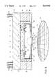
- FIG. 1shows a side cross-sectional view of a prior art probe assembly 2 for probing integrated circuit chip 4 which is disposed on surface 6 of support member 8 for integrated circuit chip 4.
- Probe assembly 2consists of a dielectric substrate 10 having a central aperture 12 therethrough. On surface 14 of substrate 10 there are disposed a plurality of electrically conducting beams which extend towards edge 18 of aperture 12.
- Conductors 16have ends 20 which bend downwardly in a direction generally perpendicular to the plane of surface 14 of substrate 10. Tips 22 of downwardly projecting electrically conducting ends 20 are disposed in electrical contact with contact locations 24 on surface 25 of integrated circuit chip 4.
- Coaxial cables 26bring electrical signals, power and ground through electrical connectors 28 at periphery 30 of substrate 10. Structure 2 of FIG.
- Conductors 16were generally made of a high strength metal such as tungsten to resist damage from use. Tungsten has an undesirably high resistivity.
- a broad aspect of the present inventionis a test probe having a plurality of electrically conducting elongated members embedded in a material. One end of each conductor is arranged for alignment with contact locations on a workpiece to be tested.
- the other end of the elongated conductorsare electrically connected to contact locations on the surface of a fan-out substrate.
- the fan-out substrateprovides space transformation of the closely spaced electrical contacts on the first side of the fan-out substrate. Contact locations having a larger spacing are on a second side of the fan out substrate.
- pinsare electrically connected to the contact locations on the second surface of the fan out substrate.
- the plurality of pins on the second surface of the fan-out substrateare inserted into a socket on a second fan-out substrate.
- the first and second space transformation substratesprovide fan out from the fine pitch of the integrated circuit I/O to a larger pitch of electrical contacts for providing signal, power and ground to the workpiece to be tested.
- the pin and socket assemblyis replaced by an interposer containing a plurality of elongated electrical connectors embedded in a layer of material which is squeezed between contact locations on the first fan-out substrate and contact locations on the second fan-out substrate.
- the test probeis part of a test apparatus and test tool.
- Another broad aspect of the present inventionis a method of fabricating the probe tip of the probe according to the present invention wherein a plurality of elongated conductors are bonded to contact locations on a substrate surface and project away therefrom.
- the elongated conductorsare wire bonded to contact locations on the substrate surface.
- the wiresproject preferably at a nonorthogonal angle from the contact locations.
- the wiresare bonded to the contact locations on the substrate are embedded in a elastomeric material to form a probe tip for the structure of the present invention.
- the elongated conductorsare embedded in an elastomeric material.
- FIG. 1is a schematic cross-section of a conventional test probe for an integrated circuit device.
- FIG. 2is a schematic diagram of one embodiment of the probe structure of the present invention.
- FIG. 3is a schematic diagram of another embodiment of the probe structure of the present invention.
- FIG. 4is an enlarged view of an elastomeric connector electrically interconnecting two space transformation substrates of the structure of FIG. 2.
- FIG. 5is an enlarged view of the probe tip within dashed circle 100 of FIGS. 2 or 3.
- FIG. 6shows the probe tip of the structure of FIG. 5 probing an integrated circuit device.
- FIGS. 7-12show the process for making the structure of FIG. 5.
- FIG. 13shows a probe tip structure without a fan-out substrate.
- FIG. 14shows the elongated conductors of the probe tip fixed by solder protuberances to contact locations on a space transformation substrate.
- FIG. 15shows the elongated conductors of the probe tip fixed by laser weld protuberances to contact locations on a space transformation substrate.
- FIG. 16shows both interposer 76 and probe tip 40 rigidly bonded to space transformer 60.
- FIGS. 2 and 3show two embodiments of the test assembly according to the present invention. Numerals common between FIGS. 2 and 3 represent the same thing.
- Probe head 40is formed from a plurality of elongated electrically conducting members 42 embedded in a material 44 which is preferably an elastomeric material 44.
- the elongated conducting members 42have ends 46 for probing contact locations on integrated circuit devices 48 of wafer 50.
- the workpieceis an integrated circuit such as a semiconductor chip or a semiconductor wafer having a plurality of chips.
- the workpiececan be any other electronic device.
- the opposite ends 52 of elongated electrical conductors 42are in electrical contact with space transformer (or fan-out substrate) 54.
- space transformer 54is a multilevel metal/ceramic substrate, a multilevel metal/polymer substrate or a printed circuit board which are typically used as packaging substrates for integrated circuit chips.
- Space transformer 54has, in the preferred embodiment, a surface layer 56 comprising a plurality of thin dielectric films, preferably polymer films such as polyimide, and a plurality of layers of electrical conductors, for example, copper conductors.
- a process for fabricating multilayer structure 56 for disposing it on surface 58 of substrate 60 to form a space transformer 54is described in U.S. patent application Ser. No.
- pins 64are standard pins used on integrated circuit chip packaging substrates. Pins 64 are inserted into socket 66 or plated through-holes in the substrate 68 which is disposed on surface 70 of second space transformer 68.
- Socket 66is a type of pin grid array (PGA) socket such as commonly disposed on a printed circuit board of an electronic computer for receiving pins from a packaging substrate.
- Second space transformer 68can be any second level integrated circuit packaging substrate, for example, a standard printed circuit board. Socket 66 is disposed on surface 70 of substrate 68.
- socket 68can be zero insertion force (ZIF) connector or the socket 68 can be replaced by through-holes in the substrate 68 wherein the through-holes have electrically conductive material surrounding the sidewalls such as a plated through-hole.
- ZIFzero insertion force
- elastomeric connector 76In the embodiment of FIG. 3, the pin 64 and socket 66 combination of the embodiment of FIG. 2 is replaced by an interposer, such as, elastomeric connector 76.
- interposersuch as, elastomeric connector 76.
- the structure of elastomeric connector 76 and the process for fabricating elastomeric connector 76is described in copending U.S. patent application Ser. No. 07/963,346 to B. Beaman et al., filed Oct. 19, 1992, entitled “THREE DIMENSIONAL HIGH PERFORMANCE INTERCONNECTION MEANS" (now U.S. Pat. No.
- the elastomeric connectorcan be opted to have one end permanently bonded to the substrate, thus forming a FRU (field replacement unit) together with the probe/substrate/connector assembly.
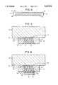
- FIG. 4shows a cross-sectional view of structure of the elastomeric connector 76 of FIG. 3.
- Connector 76is fabricated of preferably elastomeric material 78 having opposing, substantially parallel and planar surfaces 80 and 82.
- Elongated electrical conductors 84are preferably at a nonorthogonal angle to surfaces 81 and 83.
- Elongated conductors 85are preferably wires which have protuberances 86 at surface 81 of elastomeric material layer 78 and flattened protuberances 88 at surface 83 of elastomeric material layer 78.
- Flattened protuberances 88preferably have a projection on the flattened surface as shown for the structure of FIG. 14.
- Protuberance 86is preferably spherical and flattened protuberance 88 is preferably a flattened sphere.
- Connector 76is squeezed between surface 62 of substrate 54 and surface 73 of substrate 68 to provide electrical connection between end 88 of wires 85 and contact location 75 on surface 73 of substrate 68 and between end 88 or wires 85 and contact location 64 on surface 62 of substrate 54.
- connector 76can be rigidly attached to substrate 54 by solder bonding ends 88 of wires 85 to pads 64 on substrate 54 or by wire bonding ends 86 of wires 85 to pads 64 on substrate 54 in the same manner that wires 42 are bonded to pads 106 as described herein below with respect to FIG. 5.
- Wires 85can be encased in an elastomeric material in the same manner as wires 42 of FIG. 5.
- Space transformer 54is held in place with respect to second space transformer 68 by gripping means or clamping arrangement 80 which is comprised of member 82 which is perpendicularly disposed with respect to surface 70 of second space transformer 68 and member 84 which is preferably parallely disposed with respect to surface 86 of first space transformer 54.
- Member 84presses against surface 87 of space transformer 54 to hold space transformer 54 in place with respect surface 70 of space transformer 64.
- Member 82 of clamping arrangement 80can be held in place with respect to surface 70 by a screw which is inserted through member 84 at location 90 extending through the center of member 82 and screw into surface 70.
- assembly holder 94which is part of an integrated circuit test tool or apparatus having a means for depositing the probe tip ends 110 in contact with contact locations on the integrated circuit being tested.
- Members 82, 84 and 90can be made from materials such as aluminum.
- FIG. 5is a enlarged view of the region of FIGS. 2 or 3 closed in dashed circle 100 which shows the attachment of probe head 40 to substrate 60 of space transformer 54.
- elongated conductors 42are preferably wires which are at a non-orthogonal angle with respect to surface 87 of substrate 60.
- At end 102 of wire 42there is preferably a flattened protuberance 104 which is bonded (by wire bonding, solder bonding or any other known bonding technique) to electrically conducting pad 106 on surface 87 of substrate 60.
- Elastomeric material 44is substantially flush against surface 87.
- elongated electrically conducting members 42have an end 110. In the vicinity of end 110, there is optimally a cavity 112 surrounding end 110. The cavity is at surface 108 in the elastomeric material 44.
- FIG. 6shows the structure of FIG. 5 used to probe integrated circuit chip 114 which has a plurality of contact locations 116 shown as spheres such as a C4 solder balls.
- the ends 110 of conductors 42are pressed in contact with contact locations 116 for the purpose of electrically probing integrated circuit 114.
- Cavity 112provides an opening in elastomeric material 44 to permit ends 110 to be pressed towards and into solder mounds 116. Cavity 112 provides a means for solder mounds 116 to self align to ends 110 and provides a means containing solder mounds which may melt, seep or be less viscous when the probe is operated at an elevated temperature. When the probe is used to test or burn-in workpieces have flat pads as contact locations the cavities 112 can remain or be eliminated.
- FIGS. 7-13show the process for fabricating the structure of FIG. 5.
- Substrate 60 with contact locations 106 thereonis disposed in a wire bond tool.
- the top surface 122 of pad 106is coated by a method such as evaporation, sputtering or plating with soft gold or Ni/Au to provide a suitable surface for thermosonic ball bonding.
- Other bonding techniquescan be used such as thermal compression bonding, ultrasonic bonding, laser bonding and the like.
- a commonly used automatic wire bonderis modified to ball bond gold, gold alloy, copper, copper alloy, aluminum, Pt, nickel or palladium wires 120 to the pad 106 on surface 122 as shown in FIG. 7.
- the wirepreferably has a diameter of 0.001 to 0.005 inches.
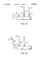
- Structure 124 of FIG. 7is the ball bonding head which has a wire 126 being fed from a reservoir of wire as in a conventional wire bonding apparatus.
- FIG. 7shows the ball bond head 124 in contact at location 126 with surface 122 of pad 106.
- FIG. 8shows the ball bonding head 124 withdrawn in the direction indicated by arrow 128 from the pad 106 and the wire 126 drawn out to leave disposed on the pad 106 surface 122 wire 130.
- the bond head 124is stationary and the substrate 60 is advanced as indicated by arrow 132.
- the bond wireis positioned at an angle preferably between 5° to 60° from vertical and then mechanically notched (or nicked) by knife edge 134 as shown in FIG. 9.
- the knife edge 134is actuated, the wire 126 is clamped and the bond head 124 is raised. The wire is pulled up and breaks at the notch or nick.
- each wireis ball bonded to adjacent contact locations which can be spaced less than 5 mils apart.
- the wireis held tight and knife edge 134 notches the wire leaving upstanding or flying leads 120 bonded to contact locations 106 in a dense array.
- FIG. 10shows the wire 126 notched (or nicked) to leave wire 120 disposed on surface 122 of pad 106.
- the wire bond head 124is retracted upwardly as indicated by arrow 136.
- the wire bond head 124has a mechanism to grip and release wire 126 so that wire 126 can be tensioned against the shear blade to sever the wire.
- a casting mold 140 as as shown in FIG. 11is disposed on surface 142 of substrate 60.
- the moldis a tubular member of any cross-sectional shape, such as circular and polygonal.
- the moldis preferably made of metal or organic materials.
- the length of the moldis preferably the height 144 of the wires 120.
- a controlled volume of liquid elastomer 146is disposed into the casting 140 mold and allowed to settle out (flow between the wires until the surface is level) before curing as shown in FIG. 13. Once the elastomer has cured, the mold is removed to provide the structure shown in FIG. 5 except for cavities 112.
- the cured elastomeris represented by reference numeral 44.
- a mold enclosing the wires 120can be used so that the liquid elastomer can be injection molded to encase the wires 120.
- the top surface of the composite polymer/wire blockcan be mechanically planarized to provide a uniform wire height and smooth polymer surface.
- a moly mask with holes located over the ends of the wire contactsis used to selectively ablate (or reactive ion etch) a cup shaped recess in the top surface of the polymer around each of the wires.
- the probe contactscan be reworked by repeating the last two process steps.
- a high compliance, high thermal stability siloxane elastomer materialis preferable for this application.
- the compliance of the cured elastomeris selected for the probe application. Where solder mounds are probed a more rigid elastomeric is used so that the probe tips are pushed into the solder mounds where a gold coated aluminum pad is being probed a more compliant elastomeric material is used to permit the wires to flex under pressure so that the probe ends in contact with the pad will move to wipe over the pad so that good electrical contact is made therewith.
- the high temperature siloxane materialis cast or injected and cured similar to other elastomeric materials. To minimize the shrinkage, the elastomer is preferably cured at lower temperature (T ⁇ 60°) followed by complete cure at higher temperatures (T ⁇ 80°).
- the use of polydimethylsiloxane based rubbersbest satisfy both the material and processing requirements.
- the thermal stability of such elastomersis limited at temperatures below 200° C. and significant outgassing is observed above 100° C.
- the thermal stabilitycan be significantly enhanced by the incorporation of 25 wt % or more diphenylsiloxane.
- enhancement in the thermal stabilityhas been demonstrated by increasing the molecular weight of the resins (oligomers) or minimizing the cross-link junction. The outgassing of the clastomers can be minimized at temperatures below 300° C.
- the high density test probeprovides a means for testing high density and high performance integrated circuits in wafer form or as discrete chips.
- the probe contactscan be designed for high performance functional testing or high temperature burn-in applications.
- the probe contactscan also be reworked several times by resurfacing the rigid polymer material that encases the wires exposing the ends of the contacts.
- the high density probe contacts described in this disclosureare designed to be used for testing semiconductor devices in either wafer form or as discrete chips.
- the high density probeuses metal wires that are bonded to a rigid substrate.
- the wiresare imbedded in a rigid polymer that has a cup shaped recess around each to the wire ends.
- the cup shaped recess 112 shown in FIG. 5provides a positive self-aligning function for chips with solder ball contacts.
- a plurality of probe heads 40can be mounted onto a space transformation substrate 60 so that a plurality of chips can be probed an burned-in simultaneously.
- An alternate embodiment of this inventionwould include straight wires instead of angled wires.
- Another alternate embodimentcould use a suspended alignment mask for aligning the chip to the wire contacts instead of the cup shaped recesses in the top surface of the rigid polymer.
- the suspended alignment maskis made by ablating holes in a thin sheet of polyimide using an excimer laser and a metal mask with the correct hole pattern.
- Another alternate embodiment of this designwould include a interposer probe assembly that could be made separately from the test substrate as described in U.S. patent application, Ser. No. 07/963,364, incorporated by reference herein above.
- This designcould be fabricated by using a copper substrate that would be etched away after the probe assembly is completed and the polymer is cured. This approach could be further modified by using an adhesion de-promoter on the wires to allow them to slide freely (along the axis of the wires) in the polymer material.
- FIG. 12shows an alternate embodiment of probe tip 40 of FIGS. 2 and 3.
- probe tip 40is fabricated to be originally fixed to the surface of a first level space transformer 54.
- Each wire 120is wire bonded directly to a pad 106 on substrate 60 so that the probe assembly 40 is rigidly fixed to the substrate 60.
- the probe head assembly 40can be fabricated via a discrete stand alone element. This can be fabricated following the process of U.S. patent application Ser. No. 07/963,348, filed Oct. 19, 1992, which has been incorporated herein by reference above. Following this fabrication process as described herein above, wires 42 of FIG. 13 are wire bonded to a surface.
- wire 42is wire bonded to a sacrificial substrate as described in the application incorporated herein.
- the sacrificial substrateis removed to leave the structure of FIG. 13.
- the sacrificial substrate to which the wires are bondedhave an array of pits which result in a protrusion 150 which can have any predetermined shape such as a hemisphere or a pyramid.
- Protrusion 150provides a raised contact for providing good electrical connection to a contact location against which it is pressed.
- probe tip assembly 40can be pressed towards surface 58 of substrate 60 so that ends 104 of FIG. 13 can be pressed against contact locations such as 106 of FIG. 5 on substrate 60.
- Protuberances 104are aligned to pads 100 on surface 58 of FIG. 5 in a manner similar to how the conductor ends 86 and 88 of the connector in FIG. 4 are aligned to pads 75 and 64 respectively.
- wire 126is ball bonded to pad 106 on substrate 60.
- An alternative processis to start with a substrate 160 as shown in FIG. 14 having contact locations 162 having an electrically conductive material 164 disposed on surface 166 of contact location 162. Electrically conductive material 164 can be solder.
- a bond leadsuch as 124 of FIG. 7 can be used to dispose end 168 of wire 170 against solder mound 164 which can be heated to melting. End 168 of wire 170 is pressed into the molten solder mound to form wire 172 embedded into a solidified solder mound 174.
- a structure similar to that of FIG. 5can be fabricated.
- FIG. 15shows another alternative embodiment of a method to fabricate the structure of FIG. 5.
- End 180 elongated electrical conductor 182is held against top surface 163 of pad 162 on substrate 160.
- a beam of light 184 from laser 186is directed at end 180 of elongated conductor 182 at the location of contact with surface 163 of pad 162.
- the end 180is laser welded to surface 163 to form protuberance 186.
- the present inventionis directed to high density test probe for testing high density and high performance integrated circuits in wafer form or as discrete chips.
- the probe contactsare designed for high performance functional testing and for high temperature burn in applications.
- the probeis formed from an elastomeric probe tip having a highly dense array of elongated electrical conductors embedded in an elastomeric material which is in electrical contact with a space transformer.
Landscapes
- Physics & Mathematics (AREA)
- General Physics & Mathematics (AREA)
- Engineering & Computer Science (AREA)
- Microelectronics & Electronic Packaging (AREA)
- Computer Hardware Design (AREA)
- Power Engineering (AREA)
- Condensed Matter Physics & Semiconductors (AREA)
- General Engineering & Computer Science (AREA)
- Measuring Leads Or Probes (AREA)
- Testing Or Measuring Of Semiconductors Or The Like (AREA)
- Manufacturing Of Electrical Connectors (AREA)
- Cooling Or The Like Of Semiconductors Or Solid State Devices (AREA)
- Multi-Conductor Connections (AREA)
Abstract
Description
This invention relates to an apparatus and test probe for integrated circuit devices and methods of use thereof.
In the microelectronics industry, before integrated circuit (IC) chips are packaged in an electronic component, such as a computer, they are tested. Testing is essential to determine whether the integrated circuit's electrical characteristics conform to the specifications to which they were designed to ensure that electronic component performs the function for which it was designed.
Testing is an expensive part of the fabrication process of contemporary computing systems. The functionality of every I/O for contemporary integrated circuit must be tested since a failure to achieve the design specification at a single I/O can render an integrated circuit unusable for a specific application. The testing is commonly done both at room temperature and at elevated temperatures to test functionality and at elevated temperatures with forced voltages and currents to burn the chips in and to test the reliability of the integrated circuit to screen out early failures.
Contemporary probes for integrated circuits are expensive to fabricate and are easily damaged. Contemporary test probes are typically fabricated on a support substrate from groups of elongated metal conductors which fan inwardly towards a central location where each conductor has an end which corresponds to a contact location on the integrated circuit chip to be tested. The metal conductors generally cantilever over an aperture in the support substrate. The wires are generally fragile and easily damage and are easily displaceable from the predetermined positions corresponding to the design positions of the contact locations on the integrated circuit being tested. These probes last only a certain number of testing operations, after which they must be replaced by an expensive replacement or reworked to recondition the probes.
FIG. 1 shows a side cross-sectional view of a prior art probe assembly 2 for probingintegrated circuit chip 4 which is disposed onsurface 6 of support member 8 forintegrated circuit chip 4. Probe assembly 2 consists of adielectric substrate 10 having acentral aperture 12 therethrough. Onsurface 14 ofsubstrate 10 there are disposed a plurality of electrically conducting beams which extend towardsedge 18 ofaperture 12.Conductors 16 haveends 20 which bend downwardly in a direction generally perpendicular to the plane ofsurface 14 ofsubstrate 10.Tips 22 of downwardly projecting electrically conductingends 20 are disposed in electrical contact withcontact locations 24 onsurface 25 of integratedcircuit chip 4.Coaxial cables 26 bring electrical signals, power and ground throughelectrical connectors 28 atperiphery 30 ofsubstrate 10. Structure 2 of FIG. 1 has the disadvantage of being expensive to fabricate and of having fragileinner ends 20 ofelectrical conductors 16. Ends 20 are easily damaged through use in probing electronic devices. Since the probe 2 is expensive to fabricate, replacement adds a substantial cost to the testing of integrated circuit devices.Conductors 16 were generally made of a high strength metal such as tungsten to resist damage from use. Tungsten has an undesirably high resistivity.
It is an object of the present invention to provide an improved high density test probe, test apparatus and method of use thereof.
It is another object of the present invention to provide an improved test probe for testing and burning-in integrated circuits.
It is another object of the present invention to provide an improved test probe and apparatus for testing integrated circuits in wafer form and as discrete integrated circuit chips.
It is an additional object of the present invention to provide probes having contacts which can be designed for high performance functional testing and for high temperature burn in applications.
It is yet another object of the present invention to provide probes having contacts which can be reworked several times by resurfacing some of the materials used to fabricate the probe of the present invention.
It is further object of the present invention to provide an improved test probe having a probe tip member containing a plurality of elongated conductors each ball bonded to electrical contact locations on space transformation substrate.
A broad aspect of the present invention is a test probe having a plurality of electrically conducting elongated members embedded in a material. One end of each conductor is arranged for alignment with contact locations on a workpiece to be tested.
In a more particular aspect of the present invention, the other end of the elongated conductors are electrically connected to contact locations on the surface of a fan-out substrate. The fan-out substrate provides space transformation of the closely spaced electrical contacts on the first side of the fan-out substrate. Contact locations having a larger spacing are on a second side of the fan out substrate.
In yet another more particular aspect of the present invention, pins are electrically connected to the contact locations on the second surface of the fan out substrate.
In another more particular aspect of the present invention, the plurality of pins on the second surface of the fan-out substrate are inserted into a socket on a second fan-out substrate. The first and second space transformation substrates provide fan out from the fine pitch of the integrated circuit I/O to a larger pitch of electrical contacts for providing signal, power and ground to the workpiece to be tested.
In another more particular aspect of the present invention, the pin and socket assembly is replaced by an interposer containing a plurality of elongated electrical connectors embedded in a layer of material which is squeezed between contact locations on the first fan-out substrate and contact locations on the second fan-out substrate.
In another more particular aspect of the present invention, the test probe is part of a test apparatus and test tool.
Another broad aspect of the present invention is a method of fabricating the probe tip of the probe according to the present invention wherein a plurality of elongated conductors are bonded to contact locations on a substrate surface and project away therefrom.
In a more particular aspect of the method according to the present invention, the elongated conductors are wire bonded to contact locations on the substrate surface. The wires project preferably at a nonorthogonal angle from the contact locations.
In another more particular aspect of the method of the present invention, the wires are bonded to the contact locations on the substrate are embedded in a elastomeric material to form a probe tip for the structure of the present invention.
In another more particular aspect of the present invention, the elongated conductors are embedded in an elastomeric material.
FIG. 1 is a schematic cross-section of a conventional test probe for an integrated circuit device.
FIG. 2 is a schematic diagram of one embodiment of the probe structure of the present invention.
FIG. 3 is a schematic diagram of another embodiment of the probe structure of the present invention.
FIG. 4 is an enlarged view of an elastomeric connector electrically interconnecting two space transformation substrates of the structure of FIG. 2.
FIG. 5 is an enlarged view of the probe tip within dashedcircle 100 of FIGS. 2 or 3.
FIG. 6 shows the probe tip of the structure of FIG. 5 probing an integrated circuit device.
FIGS. 7-12 show the process for making the structure of FIG. 5.
FIG. 13 shows a probe tip structure without a fan-out substrate.
FIG. 14 shows the elongated conductors of the probe tip fixed by solder protuberances to contact locations on a space transformation substrate.
FIG. 15 shows the elongated conductors of the probe tip fixed by laser weld protuberances to contact locations on a space transformation substrate.
FIG. 16 shows bothinterposer 76 andprobe tip 40 rigidly bonded tospace transformer 60.
Turning now to the figures, FIGS. 2 and 3 show two embodiments of the test assembly according to the present invention. Numerals common between FIGS. 2 and 3 represent the same thing.Probe head 40 is formed from a plurality of elongated electrically conductingmembers 42 embedded in amaterial 44 which is preferably anelastomeric material 44. The elongated conductingmembers 42 have ends 46 for probing contact locations on integratedcircuit devices 48 ofwafer 50. In the preferred embodiment, the workpiece is an integrated circuit such as a semiconductor chip or a semiconductor wafer having a plurality of chips. The workpiece can be any other electronic device. The opposite ends 52 of elongatedelectrical conductors 42 are in electrical contact with space transformer (or fan-out substrate) 54. In the preferred embodiment,space transformer 54 is a multilevel metal/ceramic substrate, a multilevel metal/polymer substrate or a printed circuit board which are typically used as packaging substrates for integrated circuit chips.Space transformer 54 has, in the preferred embodiment, asurface layer 56 comprising a plurality of thin dielectric films, preferably polymer films such as polyimide, and a plurality of layers of electrical conductors, for example, copper conductors. A process for fabricatingmultilayer structure 56 for disposing it onsurface 58 ofsubstrate 60 to form aspace transformer 54 is described in U.S. patent application Ser. No. 07/695,368, filed on May 3, 1991, entitled "MULTI-LAYER THIN FILM STRUCTURE AND PARALLEL PROCESSING METHOD FOR FABRICATING SAME" (now U.S. Pat. No. 5,258,236) which is assigned to the assignee of the present invention, the teaching of which is incorporated herein by reference. Details of the fabrication ofprobe head 40 and of the assembly ofprobe head
As shown in FIG. 2, onsurface 62 ofsubstrate 60, there are, a plurality ofpins 64.Surface 62 is opposite the surface 57 on whichprobe head 40 is disposed.Pins 64 are standard pins used on integrated circuit chip packaging substrates.Pins 64 are inserted into socket 66 or plated through-holes in thesubstrate 68 which is disposed onsurface 70 ofsecond space transformer 68. Socket 66 is a type of pin grid array (PGA) socket such as commonly disposed on a printed circuit board of an electronic computer for receiving pins from a packaging substrate.Second space transformer 68 can be any second level integrated circuit packaging substrate, for example, a standard printed circuit board. Socket 66 is disposed onsurface 70 ofsubstrate 68. Onopposite surface 70 ofsubstrate 68 there are disposed a plurality of electrical connectors to whichcoaxial cables 72 are electrically connected. Alternatively,socket 68 can be zero insertion force (ZIF) connector or thesocket 68 can be replaced by through-holes in thesubstrate 68 wherein the through-holes have electrically conductive material surrounding the sidewalls such as a plated through-hole.
In the embodiment of FIG. 3, thepin 64 and socket 66 combination of the embodiment of FIG. 2 is replaced by an interposer, such as,elastomeric connector 76. The structure ofelastomeric connector 76 and the process for fabricatingelastomeric connector 76 is described in copending U.S. patent application Ser. No. 07/963,346 to B. Beaman et al., filed Oct. 19, 1992, entitled "THREE DIMENSIONAL HIGH PERFORMANCE INTERCONNECTION MEANS" (now U.S. Pat. No. 5,371,654) which is assigned to the assignee of the present invention, the teaching of which is incorporated herein by reference and of which the present application is a continuation-in-part thereof, the priority date of the filing thereof being claimed herein. The elastomeric connector can be opted to have one end permanently bonded to the substrate, thus forming a FRU (field replacement unit) together with the probe/substrate/connector assembly.
FIG. 4 shows a cross-sectional view of structure of theelastomeric connector 76 of FIG. 3.Connector 76 is fabricated of preferablyelastomeric material 78 having opposing, substantially parallel andplanar surfaces elastomeric material 78, extending fromsurface 81 to 83 there are a plurality of elongatedelectrical conductors 85. Elongatedelectrical conductors 84 are preferably at a nonorthogonal angle tosurfaces Elongated conductors 85 are preferably wires which haveprotuberances 86 atsurface 81 ofelastomeric material layer 78 and flattenedprotuberances 88 atsurface 83 ofelastomeric material layer 78. Flattenedprotuberances 88 preferably have a projection on the flattened surface as shown for the structure of FIG. 14.Protuberance 86 is preferably spherical and flattenedprotuberance 88 is preferably a flattened sphere.Connector 76 is squeezed betweensurface 62 ofsubstrate 54 andsurface 73 ofsubstrate 68 to provide electrical connection betweenend 88 ofwires 85 andcontact location 75 onsurface 73 ofsubstrate 68 and betweenend 88 orwires 85 andcontact location 64 onsurface 62 ofsubstrate 54.
Alternatively, as shown in FIG. 3,connector 76 can be rigidly attached tosubstrate 54 by solder bonding ends 88 ofwires 85 topads 64 onsubstrate 54 or by wire bonding ends 86 ofwires 85 topads 64 onsubstrate 54 in the same manner thatwires 42 are bonded topads 106 as described herein below with respect to FIG. 5.Wires 85 can be encased in an elastomeric material in the same manner aswires 42 of FIG. 5.
The entire assembly ofsecond space transformer 68 and first space transformer withprobe head 40 is held in place withrespect wafer 50 byassembly holder 94 which is part of an integrated circuit test tool or apparatus having a means for depositing the probe tip ends 110 in contact with contact locations on the integrated circuit being tested.Members
FIG. 5 is a enlarged view of the region of FIGS. 2 or 3 closed in dashedcircle 100 which shows the attachment ofprobe head 40 tosubstrate 60 ofspace transformer 54. In the preferred embodiment,elongated conductors 42 are preferably wires which are at a non-orthogonal angle with respect to surface 87 ofsubstrate 60. Atend 102 ofwire 42 there is preferably a flattenedprotuberance 104 which is bonded (by wire bonding, solder bonding or any other known bonding technique) to electrically conductingpad 106 onsurface 87 ofsubstrate 60.Elastomeric material 44 is substantially flush againstsurface 87. At substantially oppositely disposedplanar surface 108 elongated electrically conductingmembers 42 have anend 110. In the vicinity ofend 110, there is optimally acavity 112surrounding end 110. The cavity is atsurface 108 in theelastomeric material 44.
FIG. 6 shows the structure of FIG. 5 used to probe integratedcircuit chip 114 which has a plurality ofcontact locations 116 shown as spheres such as a C4 solder balls. The ends 110 ofconductors 42 are pressed in contact withcontact locations 116 for the purpose of electrically probingintegrated circuit 114.Cavity 112 provides an opening inelastomeric material 44 to permit ends 110 to be pressed towards and intosolder mounds 116.Cavity 112 provides a means forsolder mounds 116 to self align toends 110 and provides a means containing solder mounds which may melt, seep or be less viscous when the probe is operated at an elevated temperature. When the probe is used to test or burn-in workpieces have flat pads as contact locations thecavities 112 can remain or be eliminated.
FIGS. 7-13 show the process for fabricating the structure of FIG. 5.Substrate 60 withcontact locations 106 thereon is disposed in a wire bond tool. Thetop surface 122 ofpad 106 is coated by a method such as evaporation, sputtering or plating with soft gold or Ni/Au to provide a suitable surface for thermosonic ball bonding. Other bonding techniques can be used such as thermal compression bonding, ultrasonic bonding, laser bonding and the like. A commonly used automatic wire bonder is modified to ball bond gold, gold alloy, copper, copper alloy, aluminum, Pt, nickel orpalladium wires 120 to thepad 106 onsurface 122 as shown in FIG. 7. The wire preferably has a diameter of 0.001 to 0.005 inches. If a metal other than Au is used, a thin passivation metal such as Au, Cr, Co, Ni or Pd can be coated over the wire by means of electroplating, or electroless plating, sputtering, e-beam evaporation or any other coating techniques known in the industry.Structure 124 of FIG. 7 is the ball bonding head which has awire 126 being fed from a reservoir of wire as in a conventional wire bonding apparatus. FIG. 7 shows theball bond head 124 in contact atlocation 126 withsurface 122 ofpad 106.
FIG. 8 shows theball bonding head 124 withdrawn in the direction indicated byarrow 128 from thepad 106 and thewire 126 drawn out to leave disposed on thepad 106surface 122wire 130. In the preferred embodiment, thebond head 124 is stationary and thesubstrate 60 is advanced as indicated byarrow 132. The bond wire is positioned at an angle preferably between 5° to 60° from vertical and then mechanically notched (or nicked) byknife edge 134 as shown in FIG. 9. Theknife edge 134 is actuated, thewire 126 is clamped and thebond head 124 is raised. The wire is pulled up and breaks at the notch or nick.
Cutting thewire 130 while it is suspended is not done in conventional wire bonding. In conventional wire bonding, such as that used to fabricate the electrical connector of U.S. Pat. No. 4,998,885, where, as shown in FIG. 8 thereof, one end of a wire is ball bonded using a wire bonded to a contact location on a substrate bent over a loop post and the other of the wire is wedge bonded to an adjacent contact location on the substrate. The loop is severed by a laser as shown in FIG. 6 and the ends melted to form balls. This process results in adjacent contact locations having different types of bonds, one a ball bond the other a wedge bond. The spacing of the adjacent pads cannot be less than about ˜20 mils because of the need to bond the wire. This spacing is unacceptable to fabricate a high density probe tip since dense integrated circuits have pad spacing less than this amount. In contradistinction, according to the present invention, each wire is ball bonded to adjacent contact locations which can be spaced less than 5 mils apart. The wire is held tight andknife edge 134 notches the wire leaving upstanding or flying leads 120 bonded to contactlocations 106 in a dense array.
When thewire 130 is severed there is left on thesurface 122 ofpad 106 an angled flyinglead 120 which is bonded to surface 122 at one end and the other end projects outwardly away from the surface. A ball can be formed on the end of thewire 130 which is not bonded to surface 122 using a laser or electrical discharge to melt the end of the wire. Techniques for this are described in co-pending U.S. patent application Ser. No. 07/963,346, filed Oct. 19, 1992, which is incorporated herein by reference above.
FIG. 10 shows thewire 126 notched (or nicked) to leavewire 120 disposed onsurface 122 ofpad 106. Thewire bond head 124 is retracted upwardly as indicated byarrow 136. Thewire bond head 124 has a mechanism to grip andrelease wire 126 so thatwire 126 can be tensioned against the shear blade to sever the wire.
After the wire bonding process is completed, a castingmold 140 as as shown in FIG. 11 is disposed onsurface 142 ofsubstrate 60. The mold is a tubular member of any cross-sectional shape, such as circular and polygonal. The mold is preferably made of metal or organic materials. The length of the mold is preferably the height 144 of thewires 120. A controlled volume ofliquid elastomer 146 is disposed into the casting 140 mold and allowed to settle out (flow between the wires until the surface is level) before curing as shown in FIG. 13. Once the elastomer has cured, the mold is removed to provide the structure shown in FIG. 5 except forcavities 112. The cured elastomer is represented byreference numeral 44. A mold enclosing thewires 120 can be used so that the liquid elastomer can be injection molded to encase thewires 120.
The top surface of the composite polymer/wire block can be mechanically planarized to provide a uniform wire height and smooth polymer surface. A moly mask with holes located over the ends of the wire contacts is used to selectively ablate (or reactive ion etch) a cup shaped recess in the top surface of the polymer around each of the wires. The probe contacts can be reworked by repeating the last two process steps.
A high compliance, high thermal stability siloxane elastomer material is preferable for this application. The compliance of the cured elastomer is selected for the probe application. Where solder mounds are probed a more rigid elastomeric is used so that the probe tips are pushed into the solder mounds where a gold coated aluminum pad is being probed a more compliant elastomeric material is used to permit the wires to flex under pressure so that the probe ends in contact with the pad will move to wipe over the pad so that good electrical contact is made therewith. The high temperature siloxane material is cast or injected and cured similar to other elastomeric materials. To minimize the shrinkage, the elastomer is preferably cured at lower temperature (T≦60°) followed by complete cure at higher temperatures (T≧80°).
Among the many commercially available clastomers, such as ECCOSIL and SYLGARD, the use of polydimethylsiloxane based rubbers best satisfy both the material and processing requirements. However, the thermal stability of such elastomers is limited at temperatures below 200° C. and significant outgassing is observed above 100° C. We have found that the thermal stability can be significantly enhanced by the incorporation of 25 wt % or more diphenylsiloxane. Further, enhancement in the thermal stability has been demonstrated by increasing the molecular weight of the resins (oligomers) or minimizing the cross-link junction. The outgassing of the clastomers can be minimized at temperatures below 300° C. by first using a thermally transient catalyst in the resin synthesis and secondly subjecting the resin to a thin film distillation to remove low molecular weight side-products. For our experiments, we have found that 25 wt % diphenylsiloxane is optimal, balancing the desired thermal stability with the increased viscosity associated with diphenylsiloxane incorporation. The optimum number average molecular weight of the resin for maximum thermal stability was found to be between 18,000 and 35,000 g/mol. Higher molecular weights were difficult to cure and too viscous, once filled, to process. Network formation was achieved by a standard hydrosilylation polymerization using a hindered platinum catalyst in a reactive silicon oil carrier.
In FIG. 10 whenbond head 124 bonds thewire 126 to thesurface 122 ofpad 106 there is formed a flattened spherical end shown as 104 in FIG. 6.
The high density test probe provides a means for testing high density and high performance integrated circuits in wafer form or as discrete chips. The probe contacts can be designed for high performance functional testing or high temperature burn-in applications. The probe contacts can also be reworked several times by resurfacing the rigid polymer material that encases the wires exposing the ends of the contacts.
The high density probe contacts described in this disclosure are designed to be used for testing semiconductor devices in either wafer form or as discrete chips. The high density probe uses metal wires that are bonded to a rigid substrate. The wires are imbedded in a rigid polymer that has a cup shaped recess around each to the wire ends. The cup shapedrecess 112 shown in FIG. 5 provides a positive self-aligning function for chips with solder ball contacts. A plurality of probe heads 40 can be mounted onto aspace transformation substrate 60 so that a plurality of chips can be probed an burned-in simultaneously.
An alternate embodiment of this invention would include straight wires instead of angled wires. Another alternate embodiment could use a suspended alignment mask for aligning the chip to the wire contacts instead of the cup shaped recesses in the top surface of the rigid polymer. The suspended alignment mask is made by ablating holes in a thin sheet of polyimide using an excimer laser and a metal mask with the correct hole pattern. Another alternate embodiment of this design would include a interposer probe assembly that could be made separately from the test substrate as described in U.S. patent application, Ser. No. 07/963,364, incorporated by reference herein above. This design could be fabricated by using a copper substrate that would be etched away after the probe assembly is completed and the polymer is cured. This approach could be further modified by using an adhesion de-promoter on the wires to allow them to slide freely (along the axis of the wires) in the polymer material.
FIG. 12 shows an alternate embodiment ofprobe tip 40 of FIGS. 2 and 3. As described herein above,probe tip 40 is fabricated to be originally fixed to the surface of a firstlevel space transformer 54. Eachwire 120 is wire bonded directly to apad 106 onsubstrate 60 so that theprobe assembly 40 is rigidly fixed to thesubstrate 60. The embodiment of FIG. 13, theprobe head assembly 40 can be fabricated via a discrete stand alone element. This can be fabricated following the process of U.S. patent application Ser. No. 07/963,348, filed Oct. 19, 1992, which has been incorporated herein by reference above. Following this fabrication process as described herein above,wires 42 of FIG. 13 are wire bonded to a surface. Rather than being wire bonded directly to a pad on a space transformation substrate,wire 42 is wire bonded to a sacrificial substrate as described in the application incorporated herein. The sacrificial substrate is removed to leave the structure of FIG. 13. At ends 102 ofwire 44 there is a flattenedball 104 caused by the wire bond operation. In a preferred embodiment the sacrificial substrate to which the wires are bonded have an array of pits which result in aprotrusion 150 which can have any predetermined shape such as a hemisphere or a pyramid.Protrusion 150 provides a raised contact for providing good electrical connection to a contact location against which it is pressed. Theclamp assembly 80 of FIGS. 2 and 3 can be modified so thatprobe tip assembly 40 can be pressed towardssurface 58 ofsubstrate 60 so that ends 104 of FIG. 13 can be pressed against contact locations such as 106 of FIG. 5 onsubstrate 60.Protuberances 104 are aligned topads 100 onsurface 58 of FIG. 5 in a manner similar to how the conductor ends 86 and 88 of the connector in FIG. 4 are aligned topads
As shown in the process of FIGS. 7 to 9,wire 126 is ball bonded to pad 106 onsubstrate 60. An alternative process is to start with asubstrate 160 as shown in FIG. 14 havingcontact locations 162 having an electricallyconductive material 164 disposed onsurface 166 ofcontact location 162. Electricallyconductive material 164 can be solder. A bond lead such as 124 of FIG. 7 can be used to disposeend 168 ofwire 170 againstsolder mound 164 which can be heated to melting.End 168 ofwire 170 is pressed into the molten solder mound to formwire 172 embedded into a solidifiedsolder mound 174. Using this process a structure similar to that of FIG. 5 can be fabricated.
FIG. 15 shows another alternative embodiment of a method to fabricate the structure of FIG. 5.
Numerals common between FIGS. 14 and 15 represent the same thing.End 180 elongatedelectrical conductor 182 is held againsttop surface 163 ofpad 162 onsubstrate 160. A beam of light 184 fromlaser 186 is directed atend 180 ofelongated conductor 182 at the location of contact withsurface 163 ofpad 162. Theend 180 is laser welded to surface 163 to formprotuberance 186.
In summary, the present invention is directed to high density test probe for testing high density and high performance integrated circuits in wafer form or as discrete chips. The probe contacts are designed for high performance functional testing and for high temperature burn in applications. The probe is formed from an elastomeric probe tip having a highly dense array of elongated electrical conductors embedded in an elastomeric material which is in electrical contact with a space transformer.
While the present invention has been described with respect to preferred embodiments, numerous modifications, changes and improvements will occur to those skilled in the art without departing from the spirit and scope of the invention.
Claims (7)
1. An electronic device probe for probing an electronic device comprising:
a first space transformer having a first surface;
said first surface having a first plurality of contact locations;
a first plurality of elongated electrical conductors each having a protuberance at one end thereof;
said protuberance of each of said plurality of elongated conductors is bonded to one of said plurality of contact locations;
each of said plurality of elongated conductors extends outwardly away from said surface to form an array of elongated conductors;
said array of elongated conductors being embedded in a material;
said elongated conductors having exposed probe tip ends at an exposed surface of said material;
said first space transformer has a second surface with a second plurality of contact locations thereon and further including a second space transformer which has a surface with a plurality of third contact thereon
said first plurality of contact locations are in electrical combination with said second plurality of contact locations by electrically conductive paths through said first space transformer, said second plurality of contact locations on said first space transformer is electrically connected to said third plurality of contact locations on said second space transformer.
2. An electronic device probe according to claim 1, further including an electrical interconnection means for electrically interconnecting said second plurality of electrical contact locations to said third plurality of electrical contact locations.
3. An electronic device probe according to claim 2, wherein said electrical interconnection means is a plurality of pins electrically connected to said second plurality of contact locations said pins are adapted for insertion into a socket which is electrically interconnected with said third plurality of contact locations.
4. An electronic device probe according to claim 2, wherein said electrical interconnection means comprises a body of elastomeric material having a fourth side and fifth side, a plurality of elongated conductors extending from said fourth side to said fifth side, each of said elongated conductors has a first end at said fourth side and a second end at said fifth side, said first ends are in electrical contact with said third plurality of contact locations and said second ends are in contact with said second plurality of contact locations.
5. An electronic device probe according to claim 2, further including a holding means for holding said first space transformer in a fixed spatial relationship with respect to said second space transformer.
6. An electronic device probe according to claim 5, wherein said holding means comprises an elongated member having a first end and second end said elongated member is fixedly attached to said second space transformer at said first end, there being a gripping means at said second end for gripping onto said first space transformer.
7. An electronic device probe according to claim 2, wherein said electrical interconnection means is an interposer between said first space transformer and said second space transformer.
Priority Applications (60)
| Application Number | Priority Date | Filing Date | Title |
|---|---|---|---|
| US08/055,485US5635846A (en) | 1992-10-19 | 1993-04-30 | Test probe having elongated conductor embedded in an elostomeric material which is mounted on a space transformer |
| US08/754,869US5821763A (en) | 1992-10-19 | 1996-11-22 | Test probe for high density integrated circuits, methods of fabrication thereof and methods of use thereof |
| US08/872,519US6334247B1 (en) | 1992-10-19 | 1997-06-11 | High density integrated circuit apparatus, test probe and methods of use thereof |
| US09/088,394US6300780B1 (en) | 1992-10-19 | 1998-06-01 | High density integrated circuit apparatus, test probe and methods of use thereof |
| US09/164,470US6295729B1 (en) | 1992-10-19 | 1998-10-01 | Angled flying lead wire bonding process |
| US09/382,834US7538565B1 (en) | 1992-10-19 | 1999-08-25 | High density integrated circuit apparatus, test probe and methods of use thereof |
| US09/871,536US6526655B2 (en) | 1992-10-19 | 2001-05-31 | Angled flying lead wire bonding process |
| US09/921,867US20070271781A9 (en) | 1992-10-19 | 2001-08-03 | High density integrated circuit apparatus, test probe and methods of use thereof |
| US10/145,661US20030048108A1 (en) | 1993-04-30 | 2002-05-14 | Structural design and processes to control probe position accuracy in a wafer test probe assembly |
| US10/202,069US7368924B2 (en) | 1993-04-30 | 2002-07-23 | Probe structure having a plurality of discrete insulated probe tips projecting from a support surface, apparatus for use thereof and methods of fabrication thereof |
| US10/342,167US6708403B2 (en) | 1992-10-19 | 2003-01-14 | Angled flying lead wire bonding process |
| US10/736,890US7495342B2 (en) | 1992-10-19 | 2003-12-16 | Angled flying lead wire bonding process |
| US11/930,016US20080112149A1 (en) | 1992-10-19 | 2007-10-30 | High density integrated circuit apparatus, test probe and methods of use thereof |
| US11/929,999US20080112148A1 (en) | 1992-10-19 | 2007-10-30 | High density integrated circuit apparatus, test probe and methods of use thereof |
| US11/929,899US20080106282A1 (en) | 1992-10-19 | 2007-10-30 | High density integrated circuit apparatus, test probe and methods of use thereof |
| US11/929,956US20080112145A1 (en) | 1992-10-19 | 2007-10-30 | High density integrated circuit apparatus, test probe and methods of use thereof |
| US11/930,039US20080132094A1 (en) | 1992-10-19 | 2007-10-30 | High density integrated circuit apparatus, test probe and methods of use thereof |
| US11/929,783US20080100318A1 (en) | 1992-10-19 | 2007-10-30 | High density integrated circuit apparatus, test probe and methods of use thereof |
| US11/929,711US20080116912A1 (en) | 1992-10-19 | 2007-10-30 | High density integrated circuit apparatus, test probe and methods of use thereof |
| US11/929,634US20080100316A1 (en) | 1992-10-19 | 2007-10-30 | High density integrated circuit apparatus, test probe and methods of use thereof |
| US11/929,944US20080123310A1 (en) | 1992-10-19 | 2007-10-30 | High density integrated circuit apparatus, test probe and methods of use thereof |
| US11/929,676US20080111568A1 (en) | 1992-10-19 | 2007-10-30 | High density integrated circuit apparatus, test probe and methods of use thereof |
| US11/929,883US20080048697A1 (en) | 1992-10-19 | 2007-10-30 | High density integrated circuit apparatus, test probe and methods of use thereof |
| US11/930,045US20080106872A1 (en) | 1992-10-19 | 2007-10-30 | High density integrated circuit apparatus, test probe and methods of use thereof |
| US11/930,026US20080047741A1 (en) | 1992-10-19 | 2007-10-30 | High density integrated circuit apparatus, test probe and methods of use thereof |
| US11/929,934US20080112144A1 (en) | 1992-10-19 | 2007-10-30 | High density integrated circuit apparatus, test probe and methods of use thereof |
| US11/930,019US20080106285A1 (en) | 1992-10-19 | 2007-10-30 | High density integrated circuit apparatus, test probe and methods of use thereof |
| US11/929,821US20080116915A1 (en) | 1992-10-19 | 2007-10-30 | High density integrated circuit apparatus, test probe and methods of use thereof |
| US11/929,873US20080048690A1 (en) | 1992-10-19 | 2007-10-30 | High density integrated circuit apparatus, test probe and methods of use thereof |
| US11/929,768US20080116913A1 (en) | 1992-10-19 | 2007-10-30 | High density integrated circuit apparatus, test probe and methods of use thereof |
| US11/929,839US20080129320A1 (en) | 1992-10-19 | 2007-10-30 | High density integrated circuit apparatus, test probe and methods of use thereof |
| US11/929,976US20080106283A1 (en) | 1992-10-19 | 2007-10-30 | High density integrated circuit apparatus, test probe and methods of use thereof |
| US11/929,982US20080106284A1 (en) | 1992-10-19 | 2007-10-30 | High density integrated circuit apparatus, test probe and methods of use thereof |
| US11/929,853US20080117611A1 (en) | 1992-10-19 | 2007-10-30 | High density integrated circuit apparatus, test probe and methods of use thereof |
| US11/929,697US20080111569A1 (en) | 1992-10-19 | 2007-10-30 | High density integrated circuit apparatus, test probe and methods of use thereof |
| US11/930,033US20080129319A1 (en) | 1992-10-19 | 2007-10-30 | High density integrated circuit apparatus, test probe and methods of use thereof |
| US11/929,991US20080117612A1 (en) | 1992-10-19 | 2007-10-30 | High density integrated circuit apparatus, test probe and methods of use thereof |
| US11/929,662US20080100317A1 (en) | 1992-10-19 | 2007-10-30 | High density integrated circuit apparatus, test probe and methods of use thereof |
| US11/929,962US20080112146A1 (en) | 1992-10-19 | 2007-10-30 | High density integrated circuit apparatus, test probe and methods of use thereof |
| US11/929,754US20080106281A1 (en) | 1992-10-19 | 2007-10-30 | High density integrated circuit apparatus, test probe and methods of use thereof |
| US11/929,911US20080111570A1 (en) | 1992-10-19 | 2007-10-30 | High density integrated circuit apparatus, test probe and methods of use thereof |
| US11/929,736US20080100324A1 (en) | 1992-10-19 | 2007-10-30 | High density integrated circuit apparatus, test probe and methods of use thereof |
| US11/929,806US20080116914A1 (en) | 1992-10-19 | 2007-10-30 | High density integrated circuit apparatus, test probe and methods of use thereof |
| US11/930,010US20080048691A1 (en) | 1992-10-19 | 2007-10-30 | High density integrated circuit apparatus, test probe and methods of use thereof |
| US11/929,968US20080112147A1 (en) | 1992-10-19 | 2007-10-30 | High density integrated circuit apparatus, test probe and methods of use thereof |
| US11/929,924US20080116916A1 (en) | 1992-10-19 | 2007-10-30 | High density integrated circuit apparatus, test probe and methods of use thereof |
| US11/930,638US20080106291A1 (en) | 1992-10-19 | 2007-10-31 | High density integrated circuit apparatus, test probe and methods of use thereof |
| US11/930,654US20080121879A1 (en) | 1992-10-19 | 2007-10-31 | High density integrated circuit apparatus, test probe and methods of use thereof |
| US11/930,005US20080117613A1 (en) | 1992-10-19 | 2008-02-01 | High density integrated circuit apparatus, test probe and methods of use thereof |
| US12/052,823US8754666B2 (en) | 1993-04-30 | 2008-03-21 | Probe structure having a plurality of discrete insulated probe tips projecting from a support surface, apparatus for use thereof and methods of fabrication thereof |
| US12/357,453US20090189288A1 (en) | 1992-10-19 | 2009-01-22 | Angled flying lead wire bonding process |
| US12/357,686US20090128176A1 (en) | 1992-10-19 | 2009-01-22 | High density integrated circuit apparatus, test probe and methods of use thereof |
| US12/548,575US20100045324A1 (en) | 1992-10-19 | 2009-08-27 | High density integrated circuit apparatus, test probe and methods of use thereof |
| US12/548,576US20100045318A1 (en) | 1992-10-19 | 2009-08-27 | High density integrated circuit apparatus, test probe and methods of use thereof |
| US12/548,580US20100045321A1 (en) | 1992-10-19 | 2009-08-27 | High density integrated circuit apparatus, test probe and methods of use thereof |
| US12/548,567US20100045320A1 (en) | 1992-10-19 | 2009-08-27 | High density integrated circuit apparatus, test probe and methods of use thereof |
| US12/548,556US20100045266A1 (en) | 1992-10-19 | 2009-08-27 | High density integrated circuit apparatus, test probe and methods of use thereof |
| US12/548,561US20100045317A1 (en) | 1992-10-19 | 2009-08-27 | High density integrated circuit apparatus, test probe and methods of use thereof |
| US12/548,537US20100052715A1 (en) | 1992-10-19 | 2009-08-27 | High density integrated circuit apparatus, test probe and methods of use thereof |
| US14/175,116US9404942B2 (en) | 1993-04-30 | 2014-02-07 | Coaxial probe structure of elongated electrical conductors projecting from a support structure |
Applications Claiming Priority (2)
| Application Number | Priority Date | Filing Date | Title |
|---|---|---|---|
| US07/963,346US5371654A (en) | 1992-10-19 | 1992-10-19 | Three dimensional high performance interconnection package |
| US08/055,485US5635846A (en) | 1992-10-19 | 1993-04-30 | Test probe having elongated conductor embedded in an elostomeric material which is mounted on a space transformer |
Related Parent Applications (1)
| Application Number | Title | Priority Date | Filing Date |
|---|---|---|---|
| US07/963,346Continuation-In-PartUS5371654A (en) | 1992-10-19 | 1992-10-19 | Three dimensional high performance interconnection package |
Related Child Applications (1)
| Application Number | Title | Priority Date | Filing Date |
|---|---|---|---|
| US08/754,869ContinuationUS5821763A (en) | 1992-10-19 | 1996-11-22 | Test probe for high density integrated circuits, methods of fabrication thereof and methods of use thereof |
Publications (1)
| Publication Number | Publication Date |
|---|---|
| US5635846Atrue US5635846A (en) | 1997-06-03 |
Family
ID=25507113
Family Applications (11)
| Application Number | Title | Priority Date | Filing Date |
|---|---|---|---|
| US07/963,346Expired - LifetimeUS5371654A (en) | 1992-10-19 | 1992-10-19 | Three dimensional high performance interconnection package |
| US08/055,485Expired - LifetimeUS5635846A (en) | 1992-10-19 | 1993-04-30 | Test probe having elongated conductor embedded in an elostomeric material which is mounted on a space transformer |
| US08/300,620Expired - LifetimeUS5531022A (en) | 1992-10-19 | 1994-09-02 | Method of forming a three dimensional high performance interconnection package |
| US08/754,869Expired - LifetimeUS5821763A (en) | 1992-10-19 | 1996-11-22 | Test probe for high density integrated circuits, methods of fabrication thereof and methods of use thereof |
| US08/872,519Expired - LifetimeUS6334247B1 (en) | 1992-10-19 | 1997-06-11 | High density integrated circuit apparatus, test probe and methods of use thereof |
| US09/088,394Expired - LifetimeUS6300780B1 (en) | 1992-10-19 | 1998-06-01 | High density integrated circuit apparatus, test probe and methods of use thereof |
| US09/382,834Expired - Fee RelatedUS7538565B1 (en) | 1992-10-19 | 1999-08-25 | High density integrated circuit apparatus, test probe and methods of use thereof |
| US09/921,867AbandonedUS20070271781A9 (en) | 1992-10-19 | 2001-08-03 | High density integrated circuit apparatus, test probe and methods of use thereof |
| US11/930,654AbandonedUS20080121879A1 (en) | 1992-10-19 | 2007-10-31 | High density integrated circuit apparatus, test probe and methods of use thereof |
| US11/930,638AbandonedUS20080106291A1 (en) | 1992-10-19 | 2007-10-31 | High density integrated circuit apparatus, test probe and methods of use thereof |
| US12/357,686AbandonedUS20090128176A1 (en) | 1992-10-19 | 2009-01-22 | High density integrated circuit apparatus, test probe and methods of use thereof |
Family Applications Before (1)
| Application Number | Title | Priority Date | Filing Date |
|---|---|---|---|
| US07/963,346Expired - LifetimeUS5371654A (en) | 1992-10-19 | 1992-10-19 | Three dimensional high performance interconnection package |
Family Applications After (9)
| Application Number | Title | Priority Date | Filing Date |
|---|---|---|---|
| US08/300,620Expired - LifetimeUS5531022A (en) | 1992-10-19 | 1994-09-02 | Method of forming a three dimensional high performance interconnection package |
| US08/754,869Expired - LifetimeUS5821763A (en) | 1992-10-19 | 1996-11-22 | Test probe for high density integrated circuits, methods of fabrication thereof and methods of use thereof |
| US08/872,519Expired - LifetimeUS6334247B1 (en) | 1992-10-19 | 1997-06-11 | High density integrated circuit apparatus, test probe and methods of use thereof |
| US09/088,394Expired - LifetimeUS6300780B1 (en) | 1992-10-19 | 1998-06-01 | High density integrated circuit apparatus, test probe and methods of use thereof |
| US09/382,834Expired - Fee RelatedUS7538565B1 (en) | 1992-10-19 | 1999-08-25 | High density integrated circuit apparatus, test probe and methods of use thereof |
| US09/921,867AbandonedUS20070271781A9 (en) | 1992-10-19 | 2001-08-03 | High density integrated circuit apparatus, test probe and methods of use thereof |
| US11/930,654AbandonedUS20080121879A1 (en) | 1992-10-19 | 2007-10-31 | High density integrated circuit apparatus, test probe and methods of use thereof |
| US11/930,638AbandonedUS20080106291A1 (en) | 1992-10-19 | 2007-10-31 | High density integrated circuit apparatus, test probe and methods of use thereof |
| US12/357,686AbandonedUS20090128176A1 (en) | 1992-10-19 | 2009-01-22 | High density integrated circuit apparatus, test probe and methods of use thereof |
Country Status (4)
| Country | Link |
|---|---|
| US (11) | US5371654A (en) |
| EP (1) | EP0593966B1 (en) |
| JP (1) | JP2514305B2 (en) |
| DE (1) | DE69322832T2 (en) |
Cited By (154)
| Publication number | Priority date | Publication date | Assignee | Title |
|---|---|---|---|---|
| US5757201A (en)* | 1996-09-11 | 1998-05-26 | Micron Electronics, Inc. | Universal testing device for electronic modules with different configurations and operating parameters |
| EP0922960A1 (en)* | 1997-12-12 | 1999-06-16 | Padar Tecnologie di Riccioni Roberto S.a.s. | Microcircuit testing device |
| US5929646A (en)* | 1996-12-13 | 1999-07-27 | International Business Machines Corporation | Interposer and module test card assembly |
| US5936417A (en)* | 1996-08-23 | 1999-08-10 | Ando Electric Co., Ltd. | Test head for IC tester |
| EP0977045A3 (en)* | 1998-07-30 | 2000-05-24 | inTEST IP Corp. | Apparatus for coupling a test head and probe card in a wafer testing system |
| US6097199A (en)* | 1998-01-22 | 2000-08-01 | Lsi Logic Corporation | Universal decoder test board |
| US6160412A (en)* | 1998-11-05 | 2000-12-12 | Wentworth Laboratories, Inc. | Impedance-matched interconnection device for connecting a vertical-pin integrated circuit probing device to integrated circuit test equipment |
| US20010054905A1 (en)* | 1993-11-16 | 2001-12-27 | Igor Y. Khandros | Probe card assembly and kit |
| US6420887B1 (en)* | 2000-06-13 | 2002-07-16 | Kulicke & Soffa Investment, Inc. | Modulated space transformer for high density buckling beam probe and method for making the same |
| US20020135388A1 (en)* | 1996-08-08 | 2002-09-26 | Gleason K. Reed | Membrane probing system with local contact scrub |
| US6515499B1 (en)* | 2000-09-28 | 2003-02-04 | Teradyne, Inc. | Modular semiconductor tester interface assembly for high performance coaxial connections |
| US20030092298A1 (en)* | 2001-11-13 | 2003-05-15 | International Business Machines Corporation | Apparatus for interconnecting electronic components |
| US6614246B1 (en)* | 1999-09-27 | 2003-09-02 | Hitachi, Ltd. | Probe structure |
| US20030199180A1 (en)* | 2002-04-19 | 2003-10-23 | Citizen Electronics Co., Ltd. | Connector integrated with a LED element, method for manufacturing the same, and a LED including the same connector |
| WO2003052436A3 (en)* | 2001-12-14 | 2004-02-12 | Intest Ip Corp | Flexible interface for a test head |
| US6734688B1 (en) | 2000-05-15 | 2004-05-11 | Teradyne, Inc. | Low compliance tester interface |
| US20040148773A1 (en)* | 1992-10-19 | 2004-08-05 | Beaman Brian Samuel | Angled flying lead wire bonding process |
| US20040163252A1 (en)* | 1993-11-16 | 2004-08-26 | Formfactor, Inc. | Contact carriers (tiles) for populating larger substrates with spring contacts |
| US6812718B1 (en)* | 1999-05-27 | 2004-11-02 | Nanonexus, Inc. | Massively parallel interface for electronic circuits |
| US20040232927A1 (en)* | 2002-05-23 | 2004-11-25 | Gleason K. Reed | Probe for testing a device under test |
| US20040249825A1 (en)* | 2003-06-05 | 2004-12-09 | International Business Machines Corporation | Administering devices with dynamic action lists |
| US20040266272A1 (en)* | 2001-02-02 | 2004-12-30 | Fujitsu Limited | Contactor for testing semiconductor device and manufacturing method thereof |
| US6846735B1 (en) | 2002-09-05 | 2005-01-25 | Bridge Semiconductor Corporation | Compliant test probe with jagged contact surface |
| US20050036374A1 (en)* | 2003-08-12 | 2005-02-17 | Masanari Nakashima | Probe card substrate |
| US20050035775A1 (en)* | 2003-08-13 | 2005-02-17 | Yu Zhou | Probe contact system using flexible printed circuit board |
| US20050040811A1 (en)* | 2001-03-15 | 2005-02-24 | Advantest Corporation | Universal test interface between a device under test and a test head |
| US20050062492A1 (en)* | 2001-08-03 | 2005-03-24 | Beaman Brian Samuel | High density integrated circuit apparatus, test probe and methods of use thereof |
| US20050099191A1 (en)* | 2003-05-23 | 2005-05-12 | Gleason K. R. | Probe for testing a device under test |
| US20050191582A1 (en)* | 2004-02-26 | 2005-09-01 | Hitachi Global Storage Technologies Netherlands B.V. | System, method, and apparatus for mechanically releasable slider processing including lapping, air bearing patterning, and debonding |
| US20050287789A1 (en)* | 2004-06-28 | 2005-12-29 | Bahadir Tunaboylu | Substrate with patterned conductive layer |
| US20060028220A1 (en)* | 2004-07-21 | 2006-02-09 | K&S Interconnect, Inc. | Reinforced probes for testing semiconductor devices |
| US7042241B2 (en) | 1997-06-10 | 2006-05-09 | Cascade Microtech, Inc. | Low-current pogo probe card |
| US7071718B2 (en) | 1995-12-01 | 2006-07-04 | Gascade Microtech, Inc. | Low-current probe card |
| US7075320B2 (en) | 2002-11-13 | 2006-07-11 | Cascade Microtech, Inc. | Probe for combined signals |
| US20060162955A1 (en)* | 2002-02-14 | 2006-07-27 | Crippen Warren S | Test card assembly |
| US20060181292A1 (en)* | 2005-02-16 | 2006-08-17 | K&S Interconnect, Inc. | Probe card assembly and method of attaching probes to the probe card assembly |
| US20060258135A1 (en)* | 2003-09-22 | 2006-11-16 | Matsushita Electtric Industrial Co., Ltd. | Semiconductor integrated circuit |
| US7148711B2 (en) | 2000-02-25 | 2006-12-12 | Cascade Microtech, Inc. | Membrane probing system |
| WO2007001391A2 (en) | 2004-12-16 | 2007-01-04 | International Business Machines Corporation | Metalized elastomeric electrical contacts |
| US7178236B2 (en) | 1999-06-04 | 2007-02-20 | Cascade Microtech, Inc. | Method for constructing a membrane probe using a depression |
| US20070057685A1 (en)* | 2005-09-14 | 2007-03-15 | Touchdown Technologies, Inc. | Lateral interposer contact design and probe card assembly |
| US20070075717A1 (en)* | 2005-09-14 | 2007-04-05 | Touchdown Technologies, Inc. | Lateral interposer contact design and probe card assembly |
| US20070126443A1 (en)* | 2001-07-11 | 2007-06-07 | Formfactor, Inc. | Method of Manufacturing A Probe Card |
| US7233160B2 (en) | 2000-12-04 | 2007-06-19 | Cascade Microtech, Inc. | Wafer probe |
| US20070152686A1 (en)* | 2004-05-21 | 2007-07-05 | January Kister | Knee probe having increased scrub motion |
| US7266889B2 (en) | 1998-07-14 | 2007-09-11 | Cascade Microtech, Inc. | Membrane probing system |
| US20080001612A1 (en)* | 2004-05-21 | 2008-01-03 | January Kister | Probes with self-cleaning blunt skates for contacting conductive pads |
| US20080048688A1 (en)* | 2000-03-17 | 2008-02-28 | Formfactor, Inc. | Methods for planarizing a semiconductor contactor |
| US20080068035A1 (en)* | 2006-09-14 | 2008-03-20 | Microprobe, Inc. | Knee probe having reduced thickness section for control of scrub motion |
| US7349223B2 (en) | 2000-05-23 | 2008-03-25 | Nanonexus, Inc. | Enhanced compliant probe card systems having improved planarity |
| US7355420B2 (en) | 2001-08-21 | 2008-04-08 | Cascade Microtech, Inc. | Membrane probing system |
| US20080088327A1 (en)* | 2006-10-11 | 2008-04-17 | January Kister | Probe cards employing probes having retaining portions for potting in a potting region |
| US7368927B2 (en) | 2004-07-07 | 2008-05-06 | Cascade Microtech, Inc. | Probe head having a membrane suspended probe |
| US7382142B2 (en) | 2000-05-23 | 2008-06-03 | Nanonexus, Inc. | High density interconnect system having rapid fabrication cycle |
| US7403028B2 (en) | 2006-06-12 | 2008-07-22 | Cascade Microtech, Inc. | Test structure and probe for differential signals |
| US7420381B2 (en) | 2004-09-13 | 2008-09-02 | Cascade Microtech, Inc. | Double sided probing structures |
| US7427868B2 (en) | 2003-12-24 | 2008-09-23 | Cascade Microtech, Inc. | Active wafer probe |
| US7443186B2 (en) | 2006-06-12 | 2008-10-28 | Cascade Microtech, Inc. | On-wafer test structures for differential signals |
| US7449899B2 (en) | 2005-06-08 | 2008-11-11 | Cascade Microtech, Inc. | Probe for high frequency signals |
| US20080297182A1 (en)* | 2007-05-29 | 2008-12-04 | Touchdown Technologies, Inc. | Semicoductor testing device with elastomer interposer |
| US7504842B2 (en) | 1997-05-28 | 2009-03-17 | Cascade Microtech, Inc. | Probe holder for testing of a test device |
| US20090075766A1 (en)* | 2007-09-14 | 2009-03-19 | Blosser Ben | Adaptors for mounting arrowheads to arrow shafts |
| US20090104736A1 (en)* | 2004-11-03 | 2009-04-23 | Tessera, Inc. | Stacked Packaging Improvements |
| US20090102495A1 (en)* | 2007-10-19 | 2009-04-23 | January Kister | Vertical guided probe array providing sideways scrub motion |
| US7535247B2 (en) | 2005-01-31 | 2009-05-19 | Cascade Microtech, Inc. | Interface for testing semiconductors |
| US7538565B1 (en)* | 1992-10-19 | 2009-05-26 | International Business Machines Corporation | High density integrated circuit apparatus, test probe and methods of use thereof |
| US20090146675A1 (en)* | 2007-12-10 | 2009-06-11 | Touchdown Technologies, Inc. | Planarizing probe card |
| US20090174423A1 (en)* | 2004-07-21 | 2009-07-09 | Klaerner Peter J | Bond Reinforcement Layer for Probe Test Cards |
| US20090174420A1 (en)* | 2008-01-08 | 2009-07-09 | Advantest Corporation | Test apparatus, probe card, and test method |
| US20090201041A1 (en)* | 2007-04-10 | 2009-08-13 | Microprobe, Inc. | Vertical Probe Array Arranged to Provide Space Transformation |
| US7579848B2 (en) | 2000-05-23 | 2009-08-25 | Nanonexus, Inc. | High density interconnect system for IC packages and interconnect assemblies |
| US7601039B2 (en) | 1993-11-16 | 2009-10-13 | Formfactor, Inc. | Microelectronic contact structure and method of making same |
| US7609077B2 (en) | 2006-06-09 | 2009-10-27 | Cascade Microtech, Inc. | Differential signal probe with integral balun |
| US7619419B2 (en) | 2005-06-13 | 2009-11-17 | Cascade Microtech, Inc. | Wideband active-passive differential signal probe |
| US7621761B2 (en) | 2000-06-20 | 2009-11-24 | Nanonexus, Inc. | Systems for testing and packaging integrated circuits |
| US20090291573A1 (en)* | 1993-11-16 | 2009-11-26 | Formfactor, Inc. | Probe card assembly and kit, and methods of making same |
| US20090293274A1 (en)* | 2008-05-29 | 2009-12-03 | January Kister | Probe bonding method having improved control of bonding material |
| US20090300914A1 (en)* | 2007-04-30 | 2009-12-10 | International Business Machines Corporation | Metallized Elastomeric Electrical Contacts |
| US7656172B2 (en) | 2005-01-31 | 2010-02-02 | Cascade Microtech, Inc. | System for testing semiconductors |
| US20100109691A1 (en)* | 2005-12-07 | 2010-05-06 | Microprobe, Inc. | Low Profile Probe Having Improved Mechanical Scrub and Reduced Contact Inductance |
| US7723999B2 (en) | 2006-06-12 | 2010-05-25 | Cascade Microtech, Inc. | Calibration structures for differential signal probing |
| US20100176832A1 (en)* | 2007-10-19 | 2010-07-15 | Microprobe, Inc. | Vertical Guided Layered Probe |
| US20100182031A1 (en)* | 2004-05-21 | 2010-07-22 | Microprobe, Inc. | Layered Probes With Core |
| US7764072B2 (en) | 2006-06-12 | 2010-07-27 | Cascade Microtech, Inc. | Differential signal probing system |
| US7771208B2 (en) | 2004-12-16 | 2010-08-10 | International Business Machines Corporation | Metalized elastomeric electrical contacts |
| US20100207652A1 (en)* | 2007-10-08 | 2010-08-19 | Amst Co., Ltd. | Method for wafer test and probe card for the same |
| US20100220752A1 (en)* | 2009-03-02 | 2010-09-02 | Polaronyx, Inc. | 810 nm Ultra-Short Pulsed Fiber Laser |
| US20110006796A1 (en)* | 2006-10-11 | 2011-01-13 | Microprobe, Inc. | Probe retention arrangement |
| US7876114B2 (en) | 2007-08-08 | 2011-01-25 | Cascade Microtech, Inc. | Differential waveguide probe |
| US7888957B2 (en) | 2008-10-06 | 2011-02-15 | Cascade Microtech, Inc. | Probing apparatus with impedance optimized interface |
| US20110062978A1 (en)* | 2004-05-21 | 2011-03-17 | Microprobe, Inc. | Multiple contact probes |
| WO2010059247A3 (en)* | 2008-11-21 | 2011-03-24 | Cascade Microtech, Inc. | Replaceable coupon for a probing apparatus |
| US7952373B2 (en) | 2000-05-23 | 2011-05-31 | Verigy (Singapore) Pte. Ltd. | Construction structures and manufacturing processes for integrated circuit wafer probe card assemblies |
| US20110165733A1 (en)* | 2005-12-23 | 2011-07-07 | Tessera, Inc. | Microelectronic packages and methods therefor |
| US8033838B2 (en) | 1996-02-21 | 2011-10-11 | Formfactor, Inc. | Microelectronic contact structure |
| USRE43503E1 (en) | 2006-06-29 | 2012-07-10 | Microprobe, Inc. | Probe skates for electrical testing of convex pad topologies |
| CN101178414B (en)* | 2006-11-02 | 2012-09-12 | 嘉兆科技有限公司 | Producing method of probe card having cantilever probes |
| US8372741B1 (en)* | 2012-02-24 | 2013-02-12 | Invensas Corporation | Method for package-on-package assembly with wire bonds to encapsulation surface |
| US8482111B2 (en) | 2010-07-19 | 2013-07-09 | Tessera, Inc. | Stackable molded microelectronic packages |
| US8485418B2 (en) | 1995-05-26 | 2013-07-16 | Formfactor, Inc. | Method of wirebonding that utilizes a gas flow within a capillary from which a wire is played out |
| USRE44407E1 (en) | 2006-03-20 | 2013-08-06 | Formfactor, Inc. | Space transformers employing wire bonds for interconnections with fine pitch contacts |
| US8618659B2 (en) | 2011-05-03 | 2013-12-31 | Tessera, Inc. | Package-on-package assembly with wire bonds to encapsulation surface |
| US8623706B2 (en) | 2010-11-15 | 2014-01-07 | Tessera, Inc. | Microelectronic package with terminals on dielectric mass |
| US20140176174A1 (en)* | 2012-12-26 | 2014-06-26 | Advanced Inquiry Systems, Inc. | Designed asperity contactors, including nanospikes for semiconductor test, and associated systems and methods |
| US8836136B2 (en) | 2011-10-17 | 2014-09-16 | Invensas Corporation | Package-on-package assembly with wire bond vias |
| US8835228B2 (en) | 2012-05-22 | 2014-09-16 | Invensas Corporation | Substrate-less stackable package with wire-bond interconnect |
| US8878353B2 (en) | 2012-12-20 | 2014-11-04 | Invensas Corporation | Structure for microelectronic packaging with bond elements to encapsulation surface |
| US8883563B1 (en) | 2013-07-15 | 2014-11-11 | Invensas Corporation | Fabrication of microelectronic assemblies having stack terminals coupled by connectors extending through encapsulation |
| US8975738B2 (en) | 2012-11-12 | 2015-03-10 | Invensas Corporation | Structure for microelectronic packaging with terminals on dielectric mass |
| US9023691B2 (en) | 2013-07-15 | 2015-05-05 | Invensas Corporation | Microelectronic assemblies with stack terminals coupled by connectors extending through encapsulation |
| US9034696B2 (en) | 2013-07-15 | 2015-05-19 | Invensas Corporation | Microelectronic assemblies having reinforcing collars on connectors extending through encapsulation |
| US9082753B2 (en) | 2013-11-12 | 2015-07-14 | Invensas Corporation | Severing bond wire by kinking and twisting |
| US9087815B2 (en) | 2013-11-12 | 2015-07-21 | Invensas Corporation | Off substrate kinking of bond wire |
| US9159708B2 (en) | 2010-07-19 | 2015-10-13 | Tessera, Inc. | Stackable molded microelectronic packages with area array unit connectors |
| US9214454B2 (en) | 2014-03-31 | 2015-12-15 | Invensas Corporation | Batch process fabrication of package-on-package microelectronic assemblies |
| US9224717B2 (en) | 2011-05-03 | 2015-12-29 | Tessera, Inc. | Package-on-package assembly with wire bonds to encapsulation surface |
| US9324681B2 (en) | 2010-12-13 | 2016-04-26 | Tessera, Inc. | Pin attachment |
| US9349706B2 (en) | 2012-02-24 | 2016-05-24 | Invensas Corporation | Method for package-on-package assembly with wire bonds to encapsulation surface |
| US9391008B2 (en) | 2012-07-31 | 2016-07-12 | Invensas Corporation | Reconstituted wafer-level package DRAM |
| US9412714B2 (en) | 2014-05-30 | 2016-08-09 | Invensas Corporation | Wire bond support structure and microelectronic package including wire bonds therefrom |
| US9476911B2 (en) | 2004-05-21 | 2016-10-25 | Microprobe, Inc. | Probes with high current carrying capability and laser machining methods |
| US9502390B2 (en) | 2012-08-03 | 2016-11-22 | Invensas Corporation | BVA interposer |
| US9530749B2 (en) | 2015-04-28 | 2016-12-27 | Invensas Corporation | Coupling of side surface contacts to a circuit platform |
| US9583411B2 (en) | 2014-01-17 | 2017-02-28 | Invensas Corporation | Fine pitch BVA using reconstituted wafer with area array accessible for testing |
| US9601454B2 (en) | 2013-02-01 | 2017-03-21 | Invensas Corporation | Method of forming a component having wire bonds and a stiffening layer |
| US9646917B2 (en) | 2014-05-29 | 2017-05-09 | Invensas Corporation | Low CTE component with wire bond interconnects |
| US9659848B1 (en) | 2015-11-18 | 2017-05-23 | Invensas Corporation | Stiffened wires for offset BVA |
| US9685365B2 (en) | 2013-08-08 | 2017-06-20 | Invensas Corporation | Method of forming a wire bond having a free end |
| US9702906B2 (en) | 2015-06-26 | 2017-07-11 | International Business Machines Corporation | Non-permanent termination structure for microprobe measurements |
| US9728527B2 (en) | 2013-11-22 | 2017-08-08 | Invensas Corporation | Multiple bond via arrays of different wire heights on a same substrate |
| US9735084B2 (en) | 2014-12-11 | 2017-08-15 | Invensas Corporation | Bond via array for thermal conductivity |
| US9761554B2 (en) | 2015-05-07 | 2017-09-12 | Invensas Corporation | Ball bonding metal wire bond wires to metal pads |
| US9812402B2 (en) | 2015-10-12 | 2017-11-07 | Invensas Corporation | Wire bond wires for interference shielding |
| US9842745B2 (en) | 2012-02-17 | 2017-12-12 | Invensas Corporation | Heat spreading substrate with embedded interconnects |
| US9852969B2 (en) | 2013-11-22 | 2017-12-26 | Invensas Corporation | Die stacks with one or more bond via arrays of wire bond wires and with one or more arrays of bump interconnects |
| US9888579B2 (en) | 2015-03-05 | 2018-02-06 | Invensas Corporation | Pressing of wire bond wire tips to provide bent-over tips |
| US9911718B2 (en) | 2015-11-17 | 2018-03-06 | Invensas Corporation | ‘RDL-First’ packaged microelectronic device for a package-on-package device |
| US9935075B2 (en) | 2016-07-29 | 2018-04-03 | Invensas Corporation | Wire bonding method and apparatus for electromagnetic interference shielding |
| US9984992B2 (en) | 2015-12-30 | 2018-05-29 | Invensas Corporation | Embedded wire bond wires for vertical integration with separate surface mount and wire bond mounting surfaces |
| US10008477B2 (en) | 2013-09-16 | 2018-06-26 | Invensas Corporation | Microelectronic element with bond elements to encapsulation surface |
| US10008469B2 (en) | 2015-04-30 | 2018-06-26 | Invensas Corporation | Wafer-level packaging using wire bond wires in place of a redistribution layer |
| US10026717B2 (en) | 2013-11-22 | 2018-07-17 | Invensas Corporation | Multiple bond via arrays of different wire heights on a same substrate |
| US10120020B2 (en) | 2016-06-16 | 2018-11-06 | Formfactor Beaverton, Inc. | Probe head assemblies and probe systems for testing integrated circuit devices |
| US10181457B2 (en) | 2015-10-26 | 2019-01-15 | Invensas Corporation | Microelectronic package for wafer-level chip scale packaging with fan-out |
| US10299368B2 (en) | 2016-12-21 | 2019-05-21 | Invensas Corporation | Surface integrated waveguides and circuit structures therefor |
| US10332854B2 (en) | 2015-10-23 | 2019-06-25 | Invensas Corporation | Anchoring structure of fine pitch bva |
| US10381326B2 (en) | 2014-05-28 | 2019-08-13 | Invensas Corporation | Structure and method for integrated circuits packaging with increased density |
| US10460958B2 (en) | 2013-08-07 | 2019-10-29 | Invensas Corporation | Method of manufacturing embedded packaging with preformed vias |
| US10490528B2 (en) | 2015-10-12 | 2019-11-26 | Invensas Corporation | Embedded wire bond wires |
| US11209460B2 (en)* | 2017-04-13 | 2021-12-28 | Kabushiki Kaisha Nihon Micronics | Electrical connection device with a short-circuit wiring pattern that reduces connection wirings |
| US20220341991A1 (en)* | 2021-04-26 | 2022-10-27 | Winbond Electronics Corp. | Chip testing apparatus and system |
| CN115280166A (en)* | 2020-03-13 | 2022-11-01 | 日本电产理德股份有限公司 | Inspection jig and substrate inspection device including the same |
| US11561243B2 (en)* | 2019-09-12 | 2023-01-24 | International Business Machines Corporation | Compliant organic substrate assembly for rigid probes |
| US20240183900A1 (en)* | 2022-12-06 | 2024-06-06 | Microtest S.P.A. | Interface element with elastic properties provided with internal electric vias for connecting a device to be tested to a testing head, and method for manufacturing said interface element |
Families Citing this family (294)
| Publication number | Priority date | Publication date | Assignee | Title |
|---|---|---|---|---|
| US5917707A (en)* | 1993-11-16 | 1999-06-29 | Formfactor, Inc. | Flexible contact structure with an electrically conductive shell |
| US5476211A (en) | 1993-11-16 | 1995-12-19 | Form Factor, Inc. | Method of manufacturing electrical contacts, using a sacrificial member |
| US6330164B1 (en)* | 1985-10-18 | 2001-12-11 | Formfactor, Inc. | Interconnect assemblies and methods including ancillary electronic component connected in immediate proximity of semiconductor device |
| JP2767670B2 (en)* | 1992-09-03 | 1998-06-18 | 株式会社村田製作所 | Electronic component chip holder and electronic component chip electrode forming method using the same |
| JPH0828580B2 (en)* | 1993-04-21 | 1996-03-21 | 日本電気株式会社 | Wiring board structure and manufacturing method thereof |
| US20030048108A1 (en)* | 1993-04-30 | 2003-03-13 | Beaman Brian Samuel | Structural design and processes to control probe position accuracy in a wafer test probe assembly |
| US5810607A (en)* | 1995-09-13 | 1998-09-22 | International Business Machines Corporation | Interconnector with contact pads having enhanced durability |
| US7368924B2 (en)* | 1993-04-30 | 2008-05-06 | International Business Machines Corporation | Probe structure having a plurality of discrete insulated probe tips projecting from a support surface, apparatus for use thereof and methods of fabrication thereof |
| US6336269B1 (en) | 1993-11-16 | 2002-01-08 | Benjamin N. Eldridge | Method of fabricating an interconnection element |
| US7200930B2 (en) | 1994-11-15 | 2007-04-10 | Formfactor, Inc. | Probe for semiconductor devices |
| US6246247B1 (en) | 1994-11-15 | 2001-06-12 | Formfactor, Inc. | Probe card assembly and kit, and methods of using same |
| US5772451A (en)* | 1993-11-16 | 1998-06-30 | Form Factor, Inc. | Sockets for electronic components and methods of connecting to electronic components |
| US20070228110A1 (en)* | 1993-11-16 | 2007-10-04 | Formfactor, Inc. | Method Of Wirebonding That Utilizes A Gas Flow Within A Capillary From Which A Wire Is Played Out |
| US6835898B2 (en) | 1993-11-16 | 2004-12-28 | Formfactor, Inc. | Electrical contact structures formed by configuring a flexible wire to have a springable shape and overcoating the wire with at least one layer of a resilient conductive material, methods of mounting the contact structures to electronic components, and applications for employing the contact structures |
| US7084656B1 (en) | 1993-11-16 | 2006-08-01 | Formfactor, Inc. | Probe for semiconductor devices |
| US6525555B1 (en)* | 1993-11-16 | 2003-02-25 | Formfactor, Inc. | Wafer-level burn-in and test |
| US6624648B2 (en) | 1993-11-16 | 2003-09-23 | Formfactor, Inc. | Probe card assembly |
| US5455390A (en)* | 1994-02-01 | 1995-10-03 | Tessera, Inc. | Microelectronics unit mounting with multiple lead bonding |
| US5706174A (en)* | 1994-07-07 | 1998-01-06 | Tessera, Inc. | Compliant microelectrionic mounting device |
| US5579207A (en)* | 1994-10-20 | 1996-11-26 | Hughes Electronics | Three-dimensional integrated circuit stacking |
| EP0792517B1 (en)* | 1994-11-15 | 2003-10-22 | Formfactor, Inc. | Electrical contact structures from flexible wire |
| US6727579B1 (en) | 1994-11-16 | 2004-04-27 | Formfactor, Inc. | Electrical contact structures formed by configuring a flexible wire to have a springable shape and overcoating the wire with at least one layer of a resilient conductive material, methods of mounting the contact structures to electronic components, and applications for employing the contact structures |
| US5495394A (en)* | 1994-12-19 | 1996-02-27 | At&T Global Information Solutions Company | Three dimensional die packaging in multi-chip modules |
| MY112945A (en)* | 1994-12-20 | 2001-10-31 | Ibm | Electronic devices comprising dielectric foamed polymers |
| EP0722198A3 (en)* | 1995-01-10 | 1996-10-23 | Texas Instruments Inc | Bonding wire with integral connection |
| US7276919B1 (en)* | 1995-04-20 | 2007-10-02 | International Business Machines Corporation | High density integral test probe |
| JP3058919B2 (en)* | 1995-05-26 | 2000-07-04 | フォームファクター,インコーポレイテッド | Fabrication of interconnects and tips using sacrificial substrates |
| US6483328B1 (en)* | 1995-11-09 | 2002-11-19 | Formfactor, Inc. | Probe card for probing wafers with raised contact elements |
| US5785538A (en)* | 1995-11-27 | 1998-07-28 | International Business Machines Corporation | High density test probe with rigid surface structure |
| US5804607A (en)* | 1996-03-21 | 1998-09-08 | International Business Machines Corporation | Process for making a foamed elastomeric polymer |
| US5726211A (en)* | 1996-03-21 | 1998-03-10 | International Business Machines Corporation | Process for making a foamed elastometric polymer |
| US6000126A (en)* | 1996-03-29 | 1999-12-14 | General Dynamics Information Systems, Inc. | Method and apparatus for connecting area grid arrays to printed wire board |
| US5700844A (en)* | 1996-04-09 | 1997-12-23 | International Business Machines Corporation | Process for making a foamed polymer |
| US6403226B1 (en) | 1996-05-17 | 2002-06-11 | 3M Innovative Properties Company | Electronic assemblies with elastomeric members made from cured, room temperature curable silicone compositions having improved stress relaxation resistance |
| US5890915A (en)* | 1996-05-17 | 1999-04-06 | Minnesota Mining And Manufacturing Company | Electrical and thermal conducting structure with resilient conducting paths |
| US5709336A (en)* | 1996-05-31 | 1998-01-20 | International Business Machines Corporation | Method of forming a solderless electrical connection with a wirebond chip |
| JP2000502810A (en) | 1996-09-13 | 2000-03-07 | インターナシヨナル・ビジネス・マシーンズ・コーポレーシヨン | Probe structure having a plurality of individual insulated probe tips protruding from a support surface, apparatus and method for using the same |
| US7282945B1 (en)* | 1996-09-13 | 2007-10-16 | International Business Machines Corporation | Wafer scale high density probe assembly, apparatus for use thereof and methods of fabrication thereof |
| EP0925513B1 (en)* | 1996-09-13 | 2010-03-24 | International Business Machines Corporation | Wafer scale high density probe assembly, apparatus for use thereof and methods of fabrication thereof |
| EP0925510B1 (en) | 1996-09-13 | 2007-04-11 | International Business Machines Corporation | Integrated compliant probe for wafer level test and burn-in |
| US6133072A (en)* | 1996-12-13 | 2000-10-17 | Tessera, Inc. | Microelectronic connector with planar elastomer sockets |
| SE511425C2 (en)* | 1996-12-19 | 1999-09-27 | Ericsson Telefon Ab L M | Packing device for integrated circuits |
| US6690185B1 (en)* | 1997-01-15 | 2004-02-10 | Formfactor, Inc. | Large contactor with multiple, aligned contactor units |
| US6365975B1 (en) | 1997-04-02 | 2002-04-02 | Tessera, Inc. | Chip with internal signal routing in external element |
| US5976964A (en) | 1997-04-22 | 1999-11-02 | Micron Technology, Inc. | Method of improving interconnect of semiconductor device by utilizing a flattened ball bond |
| US6525551B1 (en)* | 1997-05-22 | 2003-02-25 | International Business Machines Corporation | Probe structures for testing electrical interconnections to integrated circuit electronic devices |
| FR2764721B1 (en)* | 1997-06-13 | 1999-07-09 | Bull Cp8 | DEVICE FOR COMMUNICATING WITH A PORTABLE DATA MEDIUM |
| AU8280398A (en)* | 1997-06-30 | 1999-01-19 | Formfactor, Inc. | Sockets for semiconductor devices with spring contact elements |
| US6300575B1 (en)* | 1997-08-25 | 2001-10-09 | International Business Machines Corporation | Conductor interconnect with dendrites through film |
| US5977642A (en) | 1997-08-25 | 1999-11-02 | International Business Machines Corporation | Dendrite interconnect for planarization and method for producing same |
| US6040700A (en)* | 1997-09-15 | 2000-03-21 | Credence Systems Corporation | Semiconductor tester system including test head supported by wafer prober frame |
| US6160714A (en)* | 1997-12-31 | 2000-12-12 | Elpac (Usa), Inc. | Molded electronic package and method of preparation |
| JP2004506309A (en)* | 1997-12-31 | 2004-02-26 | エルパック(ユーエスエー)、インコーポレイテッド | Molded electronic package, manufacturing method and shielding method |
| US6211463B1 (en)* | 1998-01-26 | 2001-04-03 | Saint-Gobain Industrial Ceramics, Inc. | Electronic circuit package with diamond film heat conductor |
| US6016005A (en) | 1998-02-09 | 2000-01-18 | Cellarosi; Mario J. | Multilayer, high density micro circuit module and method of manufacturing same |
| US6600215B1 (en) | 1998-04-02 | 2003-07-29 | Micron Technology, Inc. | Method and apparatus for coupling a semiconductor die to die terminals |
| US5971771A (en)* | 1998-04-03 | 1999-10-26 | Faragi; Eric Joseph | Component to substrate connection and display assembly using same |
| US6720501B1 (en) | 1998-04-14 | 2004-04-13 | Formfactor, Inc. | PC board having clustered blind vias |
| US6078500A (en)* | 1998-05-12 | 2000-06-20 | International Business Machines Inc. | Pluggable chip scale package |
| US6107119A (en)* | 1998-07-06 | 2000-08-22 | Micron Technology, Inc. | Method for fabricating semiconductor components |
| US6664628B2 (en) | 1998-07-13 | 2003-12-16 | Formfactor, Inc. | Electronic component overlapping dice of unsingulated semiconductor wafer |
| JP2002523881A (en) | 1998-08-17 | 2002-07-30 | インフィネオン テクノロジース アクチエンゲゼルシャフト | Connection device for connecting electrical components on circuit carrier and method of manufacturing the same |
| US6169331B1 (en) | 1998-08-28 | 2001-01-02 | Micron Technology, Inc. | Apparatus for electrically coupling bond pads of a microelectronic device |
| US6239980B1 (en)* | 1998-08-31 | 2001-05-29 | General Electric Company | Multimodule interconnect structure and process |
| US6586835B1 (en)* | 1998-08-31 | 2003-07-01 | Micron Technology, Inc. | Compact system module with built-in thermoelectric cooling |
| US6618267B1 (en)* | 1998-09-22 | 2003-09-09 | International Business Machines Corporation | Multi-level electronic package and method for making same |
| US6190425B1 (en) | 1998-11-03 | 2001-02-20 | Zomaya Group, Inc. | Memory bar and related circuits and methods |
| US6295220B1 (en) | 1998-11-03 | 2001-09-25 | Zomaya Group, Inc. | Memory bar and related circuits and methods |
| US6854985B1 (en)* | 1998-12-16 | 2005-02-15 | Paricon Technologies Corporation | Elastomeric interconnection device and methods for making same |
| US6185107B1 (en)* | 1998-12-23 | 2001-02-06 | Raytheon Company | MEMS based tile assemblies and methods of fabrication |
| US6293804B2 (en)* | 1999-02-08 | 2001-09-25 | Ericsson Inc. | Self-aligning LCD connector assembly |
| US6419500B1 (en) | 1999-03-08 | 2002-07-16 | Kulicke & Soffa Investment, Inc. | Probe assembly having floatable buckling beam probes and apparatus for abrading the same |
| DE19912240A1 (en)* | 1999-03-18 | 2000-09-28 | Siemens Ag | Component and method for producing the component |
| US6174175B1 (en)* | 1999-04-29 | 2001-01-16 | International Business Machines Corporation | High density Z-axis connector |
| US6376769B1 (en) | 1999-05-18 | 2002-04-23 | Amerasia International Technology, Inc. | High-density electronic package, and method for making same |
| US6799976B1 (en) | 1999-07-28 | 2004-10-05 | Nanonexus, Inc. | Construction structures and manufacturing processes for integrated circuit wafer probe card assemblies |
| KR100707044B1 (en)* | 1999-05-27 | 2007-04-13 | 나노넥서스, 인코포레이티드 | Structure of integrated circuit wafer probe card assembly and its manufacturing method |
| JP4041619B2 (en)* | 1999-05-28 | 2008-01-30 | 東京エレクトロン株式会社 | Interconnector manufacturing method |
| US6717819B1 (en)* | 1999-06-01 | 2004-04-06 | Amerasia International Technology, Inc. | Solderable flexible adhesive interposer as for an electronic package, and method for making same |
| US7215131B1 (en) | 1999-06-07 | 2007-05-08 | Formfactor, Inc. | Segmented contactor |
| US6544880B1 (en) | 1999-06-14 | 2003-04-08 | Micron Technology, Inc. | Method of improving copper interconnects of semiconductor devices for bonding |
| US6617681B1 (en) | 1999-06-28 | 2003-09-09 | Intel Corporation | Interposer and method of making same |
| US6434726B1 (en) | 1999-06-29 | 2002-08-13 | Lucent Technologies Inc. | System and method of transmission using coplanar bond wires |
| US6780001B2 (en)* | 1999-07-30 | 2004-08-24 | Formfactor, Inc. | Forming tool for forming a contoured microelectronic spring mold |
| US6888362B2 (en) | 2000-11-09 | 2005-05-03 | Formfactor, Inc. | Test head assembly for electronic components with plurality of contoured microelectronic spring contacts |
| US6939474B2 (en)* | 1999-07-30 | 2005-09-06 | Formfactor, Inc. | Method for forming microelectronic spring structures on a substrate |
| US7189077B1 (en) | 1999-07-30 | 2007-03-13 | Formfactor, Inc. | Lithographic type microelectronic spring structures with improved contours |
| US6468098B1 (en)* | 1999-08-17 | 2002-10-22 | Formfactor, Inc. | Electrical contactor especially wafer level contactor using fluid pressure |
| JP2001116791A (en)* | 1999-10-20 | 2001-04-27 | Fujitsu Ltd | Electronic component test equipment and electrical connection |
| US6759858B2 (en)* | 1999-10-20 | 2004-07-06 | Intel Corporation | Integrated circuit test probe having ridge contact |
| US6441476B1 (en) | 2000-10-18 | 2002-08-27 | Seiko Epson Corporation | Flexible tape carrier with external terminals formed on interposers |
| JP3721893B2 (en) | 1999-10-20 | 2005-11-30 | セイコーエプソン株式会社 | Semiconductor devices and electronic devices |
| US6437587B1 (en)* | 1999-11-04 | 2002-08-20 | Agilent Technologies, Inc. | ICT test fixture for fine pitch testing |
| US6392428B1 (en)* | 1999-11-16 | 2002-05-21 | Eaglestone Partners I, Llc | Wafer level interposer |
| JP3681155B2 (en)* | 1999-12-22 | 2005-08-10 | 新光電気工業株式会社 | Electronic component mounting structure, electronic component device, electronic component mounting method, and electronic component device manufacturing method |
| US6848942B1 (en) | 2000-01-12 | 2005-02-01 | Molex Incorporated | Connectors having supportive barrier components |
| US6580031B2 (en) | 2000-03-14 | 2003-06-17 | Amerasia International Technology, Inc. | Method for making a flexible circuit interposer having high-aspect ratio conductors |
| JP3515479B2 (en)* | 2000-04-05 | 2004-04-05 | 北川工業株式会社 | Conductive member and method of manufacturing the same |
| TW518733B (en)* | 2000-04-08 | 2003-01-21 | Advanced Semiconductor Eng | Attaching method of heat sink for chip package |
| US6426638B1 (en)* | 2000-05-02 | 2002-07-30 | Decision Track Llc | Compliant probe apparatus |
| US6774315B1 (en)* | 2000-05-24 | 2004-08-10 | International Business Machines Corporation | Floating interposer |
| US6467138B1 (en)* | 2000-05-24 | 2002-10-22 | Vermon | Integrated connector backings for matrix array transducers, matrix array transducers employing such backings and methods of making the same |
| US6332782B1 (en) | 2000-06-19 | 2001-12-25 | International Business Machines Corporation | Spatial transformation interposer for electronic packaging |
| US6459039B1 (en) | 2000-06-19 | 2002-10-01 | International Business Machines Corporation | Method and apparatus to manufacture an electronic package with direct wiring pattern |
| US20020064931A1 (en)* | 2000-07-03 | 2002-05-30 | E. C. Ong | Method and apparatus for applying a protective over-coating to a ball-grid-array (BGA) structure |
| US7104804B2 (en)* | 2000-07-03 | 2006-09-12 | Advanced Interconnect Solutions | Method and apparatus for memory module circuit interconnection |
| US6537831B1 (en)* | 2000-07-31 | 2003-03-25 | Eaglestone Partners I, Llc | Method for selecting components for a matched set using a multi wafer interposer |
| US6812048B1 (en) | 2000-07-31 | 2004-11-02 | Eaglestone Partners I, Llc | Method for manufacturing a wafer-interposer assembly |
| US6815712B1 (en) | 2000-10-02 | 2004-11-09 | Eaglestone Partners I, Llc | Method for selecting components for a matched set from a wafer-interposer assembly |
| US6527563B2 (en)* | 2000-10-04 | 2003-03-04 | Gary A. Clayton | Grid interposer |
| US6686657B1 (en) | 2000-11-07 | 2004-02-03 | Eaglestone Partners I, Llc | Interposer for improved handling of semiconductor wafers and method of use of same |
| US6529022B2 (en) | 2000-12-15 | 2003-03-04 | Eaglestone Pareners I, Llc | Wafer testing interposer for a conventional package |
| US20020078401A1 (en)* | 2000-12-15 | 2002-06-20 | Fry Michael Andrew | Test coverage analysis system |
| US20020076854A1 (en)* | 2000-12-15 | 2002-06-20 | Pierce John L. | System, method and apparatus for constructing a semiconductor wafer-interposer using B-Stage laminates |
| US6524885B2 (en)* | 2000-12-15 | 2003-02-25 | Eaglestone Partners I, Llc | Method, apparatus and system for building an interposer onto a semiconductor wafer using laser techniques |
| US6515373B2 (en)* | 2000-12-28 | 2003-02-04 | Infineon Technologies Ag | Cu-pad/bonded/Cu-wire with self-passivating Cu-alloys |
| US6673653B2 (en)* | 2001-02-23 | 2004-01-06 | Eaglestone Partners I, Llc | Wafer-interposer using a ceramic substrate |
| US7396236B2 (en) | 2001-03-16 | 2008-07-08 | Formfactor, Inc. | Wafer level interposer |
| US6910268B2 (en) | 2001-03-27 | 2005-06-28 | Formfactor, Inc. | Method for fabricating an IC interconnect system including an in-street integrated circuit wafer via |
| US6856150B2 (en)* | 2001-04-10 | 2005-02-15 | Formfactor, Inc. | Probe card with coplanar daughter card |
| US6627980B2 (en) | 2001-04-12 | 2003-09-30 | Formfactor, Inc. | Stacked semiconductor device assembly with microelectronic spring contacts |
| US6595784B2 (en) | 2001-05-15 | 2003-07-22 | International Business Machines Corporation | Interposer member having apertures for relieving stress and increasing contact compliancy |
| JP4667652B2 (en)* | 2001-06-12 | 2011-04-13 | ローム株式会社 | Battery pack and manufacturing method thereof |
| US6784376B1 (en)* | 2001-08-16 | 2004-08-31 | Amkor Technology, Inc. | Solderable injection-molded integrated circuit substrate and method therefor |
| US6930256B1 (en) | 2002-05-01 | 2005-08-16 | Amkor Technology, Inc. | Integrated circuit substrate having laser-embedded conductive patterns and method therefor |
| US7334326B1 (en) | 2001-06-19 | 2008-02-26 | Amkor Technology, Inc. | Method for making an integrated circuit substrate having embedded passive components |
| EP1407280B1 (en)* | 2001-07-11 | 2005-11-23 | Formfactor, Inc. | Method of manufacturing a probe card |
| US6627984B2 (en)* | 2001-07-24 | 2003-09-30 | Dense-Pac Microsystems, Inc. | Chip stack with differing chip package types |
| US6784656B2 (en)* | 2001-08-30 | 2004-08-31 | Teradyne, Inc. | Hybrid conductor-board for multi-conductor routing |
| US6821625B2 (en) | 2001-09-27 | 2004-11-23 | International Business Machines Corporation | Thermal spreader using thermal conduits |
| US6590278B1 (en)* | 2002-01-08 | 2003-07-08 | International Business Machines Corporation | Electronic package |
| US7249954B2 (en) | 2002-02-26 | 2007-07-31 | Paricon Technologies Corporation | Separable electrical interconnect with anisotropic conductive elastomer for translating footprint |
| US7399661B2 (en) | 2002-05-01 | 2008-07-15 | Amkor Technology, Inc. | Method for making an integrated circuit substrate having embedded back-side access conductors and vias |
| US6930257B1 (en) | 2002-05-01 | 2005-08-16 | Amkor Technology, Inc. | Integrated circuit substrate having laminated laser-embedded circuit layers |
| US9691635B1 (en) | 2002-05-01 | 2017-06-27 | Amkor Technology, Inc. | Buildup dielectric layer having metallization pattern semiconductor package fabrication method |
| US7633765B1 (en) | 2004-03-23 | 2009-12-15 | Amkor Technology, Inc. | Semiconductor package including a top-surface metal layer for implementing circuit features |
| US7548430B1 (en) | 2002-05-01 | 2009-06-16 | Amkor Technology, Inc. | Buildup dielectric and metallization process and semiconductor package |
| US7670962B2 (en) | 2002-05-01 | 2010-03-02 | Amkor Technology, Inc. | Substrate having stiffener fabrication method |
| US7412639B2 (en)* | 2002-05-24 | 2008-08-12 | Verigy (Singapore) Pte. Ltd. | System and method for testing circuitry on a wafer |
| US6813804B2 (en)* | 2002-06-06 | 2004-11-09 | Samsung Electronics Co., Ltd. | Apparatus and method for cleaning probe card contacts |
| US6974330B2 (en)* | 2002-08-08 | 2005-12-13 | Micron Technology, Inc. | Electronic devices incorporating electrical interconnections with improved reliability and methods of fabricating same |
| DE10242646A1 (en)* | 2002-09-13 | 2004-03-25 | Magcode Ag | Electrical connection device between current or data source device and current or data reception device, uses elastically mounted contact elements acted on by pressure bridge |
| US6877992B2 (en)* | 2002-11-01 | 2005-04-12 | Airborn, Inc. | Area array connector having stacked contacts for improved current carrying capacity |
| US7122760B2 (en)* | 2002-11-25 | 2006-10-17 | Formfactor, Inc. | Using electric discharge machining to manufacture probes |
| US6945827B2 (en)* | 2002-12-23 | 2005-09-20 | Formfactor, Inc. | Microelectronic contact structure |
| JP2004206914A (en)* | 2002-12-24 | 2004-07-22 | Hitachi Ltd | Land grid array connector and connection structure |
| US6839965B2 (en)* | 2003-02-06 | 2005-01-11 | R-Tec Corporation | Method of manufacturing a resistor connector |
| US20040160742A1 (en)* | 2003-02-14 | 2004-08-19 | Weiss Roger E. | Three-dimensional electrical device packaging employing low profile elastomeric interconnection |
| JP2005010052A (en)* | 2003-06-19 | 2005-01-13 | Japan Electronic Materials Corp | Probe card |
| US6967556B2 (en)* | 2003-06-30 | 2005-11-22 | International Business Machines Corporation | High power space transformer |
| AU2003247705A1 (en)* | 2003-07-02 | 2005-02-15 | Paricon Technologies Corporation | Pin-array, separable, compliant electrical contact member |
| EP1657750B1 (en)* | 2003-08-18 | 2018-12-05 | Sanken Electric Co., Ltd. | Semiconductor device |
| GB2406722A (en)* | 2003-10-02 | 2005-04-06 | Agilent Technologies Inc | High frequency electrical module |
| US6814589B1 (en) | 2003-10-22 | 2004-11-09 | International Business Machines Corporation | Electrical connector with elastomeric element and restrainer member to offset relaxation of the elastomer |
| JP2005150263A (en)* | 2003-11-13 | 2005-06-09 | Nitto Denko Corp | Double-sided wiring circuit board |
| KR20050065038A (en)* | 2003-12-24 | 2005-06-29 | 삼성전기주식회사 | Printed circuit board and package having oblique via |
| US6832917B1 (en) | 2004-01-16 | 2004-12-21 | Intercon Systems, Inc. | Interposer assembly |
| US6945791B2 (en)* | 2004-02-10 | 2005-09-20 | International Business Machines Corporation | Integrated circuit redistribution package |
| US20050190810A1 (en)* | 2004-02-27 | 2005-09-01 | Stuart Butterworth | Contact-bonded optically pumped semiconductor laser structure |
| US7282932B2 (en) | 2004-03-02 | 2007-10-16 | Micron Technology, Inc. | Compliant contact pin assembly, card system and methods thereof |
| JP2005259475A (en)* | 2004-03-10 | 2005-09-22 | Jst Mfg Co Ltd | Anisotropic conductive sheet |
| US11081370B2 (en) | 2004-03-23 | 2021-08-03 | Amkor Technology Singapore Holding Pte. Ltd. | Methods of manufacturing an encapsulated semiconductor device |
| US10811277B2 (en) | 2004-03-23 | 2020-10-20 | Amkor Technology, Inc. | Encapsulated semiconductor package |
| JP4509835B2 (en)* | 2004-03-29 | 2010-07-21 | パナソニック株式会社 | Cell, package device, and method for manufacturing package device |
| US7145238B1 (en) | 2004-05-05 | 2006-12-05 | Amkor Technology, Inc. | Semiconductor package and substrate having multi-level vias |
| DE102004027788A1 (en)* | 2004-06-08 | 2006-01-05 | Infineon Technologies Ag | Semiconductor base component for semiconductor component pile, has boundary regions of substrate surrounding chip, with elastic contact unit which is electrically connected with regions of distribution plate |
| US7105918B2 (en)* | 2004-07-29 | 2006-09-12 | Micron Technology, Inc. | Interposer with flexible solder pad elements and methods of manufacturing the same |
| US7262368B2 (en)* | 2004-08-13 | 2007-08-28 | Tessera, Inc. | Connection structures for microelectronic devices and methods for forming such structures |
| US7172431B2 (en)* | 2004-08-27 | 2007-02-06 | International Business Machines Corporation | Electrical connector design and contact geometry and method of use thereof and methods of fabrication thereof |
| SG120200A1 (en)* | 2004-08-27 | 2006-03-28 | Micron Technology Inc | Slanted vias for electrical circuits on circuit boards and other substrates |
| DE202005021436U1 (en)* | 2004-11-02 | 2008-02-14 | Cascade Microtech, Inc., Beaverton | Optically enhanced digital imaging system |
| US8646675B2 (en) | 2004-11-02 | 2014-02-11 | Hid Global Gmbh | Laying apparatus, contact-making apparatus, movement system, laying and contact-making unit, production system, method for production and a transponder unit |
| US6991473B1 (en) | 2004-11-30 | 2006-01-31 | International Business Machines Corporation | Electrical connector with elastomeric pad having compressor fingers each including a filler member to mitigate relaxation of the elastomer |
| KR100706228B1 (en)* | 2004-12-07 | 2007-04-11 | 삼성전자주식회사 | Apparatus and method for testing electrical properties of semiconductor objects |
| US7404513B2 (en)* | 2004-12-30 | 2008-07-29 | Texas Instruments Incorporated | Wire bonds having pressure-absorbing balls |
| US7928591B2 (en)* | 2005-02-11 | 2011-04-19 | Wintec Industries, Inc. | Apparatus and method for predetermined component placement to a target platform |
| US20070187844A1 (en) | 2006-02-10 | 2007-08-16 | Wintec Industries, Inc. | Electronic assembly with detachable components |
| US8826531B1 (en) | 2005-04-05 | 2014-09-09 | Amkor Technology, Inc. | Method for making an integrated circuit substrate having laminated laser-embedded circuit layers |
| DE102005024133B4 (en)* | 2005-05-23 | 2007-10-31 | Msc Microcomputers Systems Components Vertriebs Gmbh | Elastomeric connector |
| US7262134B2 (en)* | 2005-09-01 | 2007-08-28 | Micron Technology, Inc. | Microfeature workpieces and methods for forming interconnects in microfeature workpieces |
| US7877866B1 (en)* | 2005-10-26 | 2011-02-01 | Second Sight Medical Products, Inc. | Flexible circuit electrode array and method of manufacturing the same |
| US7307348B2 (en)* | 2005-12-07 | 2007-12-11 | Micron Technology, Inc. | Semiconductor components having through wire interconnects (TWI) |
| US7843202B2 (en)* | 2005-12-21 | 2010-11-30 | Formfactor, Inc. | Apparatus for testing devices |
| US20070152685A1 (en)* | 2006-01-03 | 2007-07-05 | Formfactor, Inc. | A probe array structure and a method of making a probe array structure |
| TWI336608B (en)* | 2006-01-31 | 2011-01-21 | Sony Corp | Printed circuit board assembly and method of manufacturing the same |
| KR101025895B1 (en)* | 2006-06-08 | 2011-03-30 | 니혼 하츠쵸 가부시키가이샤 | Probe card |
| JP2008021637A (en)* | 2006-06-12 | 2008-01-31 | Fujikura Ltd | Socket, manufacturing method thereof, and semiconductor device |
| US7971339B2 (en) | 2006-09-26 | 2011-07-05 | Hid Global Gmbh | Method and apparatus for making a radio frequency inlay |
| US8286332B2 (en) | 2006-09-26 | 2012-10-16 | Hid Global Gmbh | Method and apparatus for making a radio frequency inlay |
| US7589398B1 (en) | 2006-10-04 | 2009-09-15 | Amkor Technology, Inc. | Embedded metal features structure |
| US7550857B1 (en) | 2006-11-16 | 2009-06-23 | Amkor Technology, Inc. | Stacked redistribution layer (RDL) die assembly package |
| US8021931B2 (en)* | 2006-12-11 | 2011-09-20 | Stats Chippac, Inc. | Direct via wire bonding and method of assembling the same |
| US7535239B1 (en)* | 2006-12-14 | 2009-05-19 | Xilinx, Inc. | Probe card configured for interchangeable heads |
| US7750250B1 (en) | 2006-12-22 | 2010-07-06 | Amkor Technology, Inc. | Blind via capture pad structure |
| US7752752B1 (en) | 2007-01-09 | 2010-07-13 | Amkor Technology, Inc. | Method of fabricating an embedded circuit pattern |
| KR100882512B1 (en)* | 2007-04-25 | 2009-02-10 | 윌테크놀러지(주) | Probe card |
| JP2009010358A (en)* | 2007-05-28 | 2009-01-15 | Panasonic Corp | Module with built-in electronic component and its manufacturing method |
| US8323771B1 (en) | 2007-08-15 | 2012-12-04 | Amkor Technology, Inc. | Straight conductor blind via capture pad structure and fabrication method |
| US8536665B2 (en)* | 2007-08-22 | 2013-09-17 | The Hong Kong Polytechnic University | Fabrication of piezoelectric single crystalline thin layer on silicon wafer |
| EP2040201B1 (en) | 2007-09-18 | 2010-11-17 | HID Global Ireland Teoranta | Method for bonding a wire conductor laid on a substrate |
| US7888955B2 (en) | 2007-09-25 | 2011-02-15 | Formfactor, Inc. | Method and apparatus for testing devices using serially controlled resources |
| US7977959B2 (en) | 2007-09-27 | 2011-07-12 | Formfactor, Inc. | Method and apparatus for testing devices using serially controlled intelligent switches |
| CN101316014B (en)* | 2007-10-17 | 2012-02-01 | 番禺得意精密电子工业有限公司 | Electric connection device and assembly method thereof |
| WO2009096318A1 (en)* | 2008-02-01 | 2009-08-06 | Nhk Spring Co., Ltd. | Probe unit |
| JP2009239261A (en)* | 2008-03-07 | 2009-10-15 | Panasonic Corp | Electronic unit and electronic apparatus |
| US20090224793A1 (en)* | 2008-03-07 | 2009-09-10 | Formfactor, Inc. | Method And Apparatus For Designing A Custom Test System |
| US8122309B2 (en)* | 2008-03-11 | 2012-02-21 | Formfactor, Inc. | Method and apparatus for processing failures during semiconductor device testing |
| US8095841B2 (en) | 2008-08-19 | 2012-01-10 | Formfactor, Inc. | Method and apparatus for testing semiconductor devices with autonomous expected value generation |
| US7944225B2 (en)* | 2008-09-26 | 2011-05-17 | Formfactor, Inc. | Method and apparatus for providing a tester integrated circuit for testing a semiconductor device under test |
| US7982305B1 (en)* | 2008-10-20 | 2011-07-19 | Maxim Integrated Products, Inc. | Integrated circuit package including a three-dimensional fan-out / fan-in signal routing |
| US8872329B1 (en) | 2009-01-09 | 2014-10-28 | Amkor Technology, Inc. | Extended landing pad substrate package structure and method |
| WO2010096714A2 (en)* | 2009-02-19 | 2010-08-26 | Touchdown Technologies, Inc. | Probe head for a microelectronic contactor assembly, the probe head having smt electronic components thereon |
| WO2010104913A1 (en)* | 2009-03-10 | 2010-09-16 | Johnstech International | Electrically conductive pins for microcircuit tester |
| US8222912B2 (en)* | 2009-03-12 | 2012-07-17 | Sv Probe Pte. Ltd. | Probe head structure for probe test cards |
| US7960827B1 (en) | 2009-04-09 | 2011-06-14 | Amkor Technology, Inc. | Thermal via heat spreader package and method |
| US8623753B1 (en) | 2009-05-28 | 2014-01-07 | Amkor Technology, Inc. | Stackable protruding via package and method |
| US8222538B1 (en) | 2009-06-12 | 2012-07-17 | Amkor Technology, Inc. | Stackable via package and method |
| US9355962B2 (en)* | 2009-06-12 | 2016-05-31 | Stats Chippac Ltd. | Integrated circuit package stacking system with redistribution and method of manufacture thereof |
| US8471154B1 (en) | 2009-08-06 | 2013-06-25 | Amkor Technology, Inc. | Stackable variable height via package and method |
| US8796561B1 (en) | 2009-10-05 | 2014-08-05 | Amkor Technology, Inc. | Fan out build up substrate stackable package and method |
| KR20110041179A (en)* | 2009-10-15 | 2011-04-21 | 한국전자통신연구원 | Package structure |
| US8937381B1 (en) | 2009-12-03 | 2015-01-20 | Amkor Technology, Inc. | Thin stackable package and method |
| US9691734B1 (en) | 2009-12-07 | 2017-06-27 | Amkor Technology, Inc. | Method of forming a plurality of electronic component packages |
| US8278752B2 (en) | 2009-12-23 | 2012-10-02 | Intel Corporation | Microelectronic package and method for a compression-based mid-level interconnect |
| US8536462B1 (en) | 2010-01-22 | 2013-09-17 | Amkor Technology, Inc. | Flex circuit package and method |
| US8476538B2 (en)* | 2010-03-08 | 2013-07-02 | Formfactor, Inc. | Wiring substrate with customization layers |
| US7928552B1 (en) | 2010-03-12 | 2011-04-19 | Stats Chippac Ltd. | Integrated circuit packaging system with multi-tier conductive interconnects and method of manufacture thereof |
| US9496152B2 (en)* | 2010-03-12 | 2016-11-15 | STATS ChipPAC Pte. Ltd. | Carrier system with multi-tier conductive posts and method of manufacture thereof |
| US8643394B2 (en)* | 2010-04-16 | 2014-02-04 | Taiwan Semiconductor Manufacturing Company, Ltd. | Non-reflow probe card structure |
| US8407888B2 (en)* | 2010-05-07 | 2013-04-02 | Oracle International Corporation | Method of assembling a circuit board assembly |
| US8300423B1 (en) | 2010-05-25 | 2012-10-30 | Amkor Technology, Inc. | Stackable treated via package and method |
| US8294276B1 (en) | 2010-05-27 | 2012-10-23 | Amkor Technology, Inc. | Semiconductor device and fabricating method thereof |
| US8411459B2 (en) | 2010-06-10 | 2013-04-02 | Taiwan Semiconductor Manufacturing Company, Ltd | Interposer-on-glass package structures |
| US8999179B2 (en) | 2010-07-13 | 2015-04-07 | Taiwan Semiconductor Manufacturing Company, Ltd. | Conductive vias in a substrate |
| US8338229B1 (en) | 2010-07-30 | 2012-12-25 | Amkor Technology, Inc. | Stackable plasma cleaned via package and method |
| US8717775B1 (en) | 2010-08-02 | 2014-05-06 | Amkor Technology, Inc. | Fingerprint sensor package and method |
| US8337657B1 (en) | 2010-10-27 | 2012-12-25 | Amkor Technology, Inc. | Mechanical tape separation package and method |
| US8482134B1 (en) | 2010-11-01 | 2013-07-09 | Amkor Technology, Inc. | Stackable package and method |
| US9748154B1 (en) | 2010-11-04 | 2017-08-29 | Amkor Technology, Inc. | Wafer level fan out semiconductor device and manufacturing method thereof |
| US8970240B2 (en)* | 2010-11-04 | 2015-03-03 | Cascade Microtech, Inc. | Resilient electrical interposers, systems that include the interposers, and methods for using and forming the same |
| US8525318B1 (en) | 2010-11-10 | 2013-09-03 | Amkor Technology, Inc. | Semiconductor device and fabricating method thereof |
| US8557629B1 (en) | 2010-12-03 | 2013-10-15 | Amkor Technology, Inc. | Semiconductor device having overlapped via apertures |
| US8535961B1 (en) | 2010-12-09 | 2013-09-17 | Amkor Technology, Inc. | Light emitting diode (LED) package and method |
| US9721872B1 (en) | 2011-02-18 | 2017-08-01 | Amkor Technology, Inc. | Methods and structures for increasing the allowable die size in TMV packages |
| US9013011B1 (en) | 2011-03-11 | 2015-04-21 | Amkor Technology, Inc. | Stacked and staggered die MEMS package and method |
| KR101140113B1 (en) | 2011-04-26 | 2012-04-30 | 앰코 테크놀로지 코리아 주식회사 | Semiconductor device |
| US8653674B1 (en) | 2011-09-15 | 2014-02-18 | Amkor Technology, Inc. | Electronic component package fabrication method and structure |
| US8633598B1 (en) | 2011-09-20 | 2014-01-21 | Amkor Technology, Inc. | Underfill contacting stacking balls package fabrication method and structure |
| US9029962B1 (en) | 2011-10-12 | 2015-05-12 | Amkor Technology, Inc. | Molded cavity substrate MEMS package fabrication method and structure |
| JP2013098451A (en)* | 2011-11-04 | 2013-05-20 | Sumitomo Electric Ind Ltd | Semiconductor device and wiring board |
| US8680684B2 (en)* | 2012-01-09 | 2014-03-25 | Invensas Corporation | Stackable microelectronic package structures |
| US20130215586A1 (en)* | 2012-02-16 | 2013-08-22 | Ibiden Co., Ltd. | Wiring substrate |
| US9390998B2 (en)* | 2012-02-17 | 2016-07-12 | Invensas Corporation | Heat spreading substrate |
| US9069014B2 (en)* | 2012-06-30 | 2015-06-30 | Intel Corporation | Wire probe assembly and forming process for die testing |
| US8540136B1 (en)* | 2012-09-06 | 2013-09-24 | Taiwan Semiconductor Manufacturing Company, Ltd. | Methods for stud bump formation and apparatus for performing the same |
| US9385052B2 (en) | 2012-09-14 | 2016-07-05 | STATS ChipPAC Pte. Ltd. | Semiconductor device and method of forming build-up interconnect structures over carrier for testing at interim stages |
| US9443797B2 (en) | 2012-09-14 | 2016-09-13 | STATS ChipPAC Pte. Ltd. | Semiconductor device having wire studs as vertical interconnect in FO-WLP |
| US9818734B2 (en) | 2012-09-14 | 2017-11-14 | STATS ChipPAC Pte. Ltd. | Semiconductor device and method of forming build-up interconnect structures over a temporary substrate |
| US9799592B2 (en) | 2013-11-19 | 2017-10-24 | Amkor Technology, Inc. | Semicondutor device with through-silicon via-less deep wells |
| KR101366461B1 (en) | 2012-11-20 | 2014-02-26 | 앰코 테크놀로지 코리아 주식회사 | Semiconductor device and manufacturing method thereof |
| US10266402B2 (en) | 2012-11-20 | 2019-04-23 | Formfactor, Inc. | Contactor devices with carbon nanotube probes embedded in a flexible film and processes of making such |
| CN103091622B (en)* | 2013-01-18 | 2015-09-30 | 宁波三星智能电气有限公司 | FCT multistation proving installation |
| KR101488590B1 (en) | 2013-03-29 | 2015-01-30 | 앰코 테크놀로지 코리아 주식회사 | Semiconductor device and manufacturing method thereof |
| US9297971B2 (en)* | 2013-04-26 | 2016-03-29 | Oracle International Corporation | Hybrid-integrated photonic chip package with an interposer |
| US9459285B2 (en) | 2013-07-10 | 2016-10-04 | Globalfoundries Inc. | Test probe coated with conductive elastomer for testing of backdrilled plated through holes in printed circuit board assembly |
| US9365947B2 (en) | 2013-10-04 | 2016-06-14 | Invensas Corporation | Method for preparing low cost substrates |
| KR101607981B1 (en) | 2013-11-04 | 2016-03-31 | 앰코 테크놀로지 코리아 주식회사 | Interposer and method for manufacturing the same, and semiconductor package using the same |
| US9209110B2 (en) | 2014-05-07 | 2015-12-08 | Qualcomm Incorporated | Integrated device comprising wires as vias in an encapsulation layer |
| TWI587412B (en)* | 2014-05-08 | 2017-06-11 | 矽品精密工業股份有限公司 | Package structures and methods for fabricating the same |
| JP6271463B2 (en)* | 2015-03-11 | 2018-01-31 | 東芝メモリ株式会社 | Semiconductor device |
| US9893017B2 (en) | 2015-04-09 | 2018-02-13 | STATS ChipPAC Pte. Ltd. | Double-sided semiconductor package and dual-mold method of making same |
| TWI716476B (en)* | 2015-10-23 | 2021-01-21 | 新加坡商海特根微光學公司 | Electrical-contact assemblies |
| US9831155B2 (en)* | 2016-03-11 | 2017-11-28 | Nanya Technology Corporation | Chip package having tilted through silicon via |
| US9960328B2 (en) | 2016-09-06 | 2018-05-01 | Amkor Technology, Inc. | Semiconductor device and manufacturing method thereof |
| WO2018089798A1 (en)* | 2016-11-12 | 2018-05-17 | Sierra Circuits, Inc. | Integrated circuit wafer integration with catalytic laminate or adhesive |
| US9922951B1 (en) | 2016-11-12 | 2018-03-20 | Sierra Circuits, Inc. | Integrated circuit wafer integration with catalytic laminate or adhesive |
| US10302694B2 (en)* | 2016-12-27 | 2019-05-28 | Texas Instruments Incorporated | Interposer based test program evaluation |
| US10600739B1 (en)* | 2017-09-28 | 2020-03-24 | Hrl Laboratories, Llc | Interposer with interconnects and methods of manufacturing the same |
| TWI626453B (en)* | 2017-09-29 | 2018-06-11 | 中華精測科技股份有限公司 | Probe assembly and capacitive space transformer thereof |
| US10658331B2 (en)* | 2018-08-28 | 2020-05-19 | Ferric Inc. | Processor module with integrated packaged power converter |
| US10367415B1 (en)* | 2018-08-28 | 2019-07-30 | Ferric Inc. | Processor module with integrated packaged power converter |
| KR102538704B1 (en)* | 2018-12-04 | 2023-06-01 | 에스케이하이닉스 주식회사 | Stack package including flexible bridge die |
| KR102674087B1 (en)* | 2019-09-06 | 2024-06-12 | 에스케이하이닉스 주식회사 | Semiconductor package including electromagnetic interference shielding layer |
| CN111403307B (en)* | 2020-03-26 | 2023-09-29 | 环鸿电子(昆山)有限公司 | Integrated circuit test module and preparation method thereof |
| CN111766416B (en)* | 2020-08-14 | 2020-12-08 | 强一半导体(苏州)有限公司 | Docking method of guide plate MEMS (micro-electromechanical systems) probe structure and switching layer |
| CN111968961B (en)* | 2020-08-24 | 2022-08-12 | 浙江集迈科微电子有限公司 | Sidewall interconnection plate and manufacturing process thereof |
| KR102466911B1 (en)* | 2020-09-28 | 2022-11-14 | 주식회사 디아이티 | Multilayer ceramic substrate having connecting means with frame and method of manufacturing the same |
| US11885830B2 (en)* | 2021-01-15 | 2024-01-30 | Lumentum Operations Llc | Probe tip assembly for testing optical components |
| JP7576376B2 (en)* | 2021-03-12 | 2024-10-31 | パナソニックオートモーティブシステムズ株式会社 | Inter-board connection structure and power conversion device |
| CN115151067B (en)* | 2021-03-30 | 2025-05-23 | 深圳市江波龙电子股份有限公司 | Manufacturing method of switching test board, switching test board and test mechanism |
| CN113655375B (en)* | 2021-09-18 | 2024-05-14 | 深圳市浦洛电子科技有限公司 | Online test burning equipment |
| EP4156253A1 (en)* | 2021-09-22 | 2023-03-29 | Infineon Technologies Austria AG | Resin encapsulated semiconductor package comprising an external recess with exposed electrical contacts and a semiconductor module using the same |
| US11929673B2 (en) | 2021-10-29 | 2024-03-12 | Ferric Inc. | Two-stage voltage converters for microprocessors |
| US12408303B2 (en)* | 2022-07-27 | 2025-09-02 | Hewlett Packard Enterprise Development Lp | Elastomer embedded multipoint contact cooling |
Citations (43)
| Publication number | Priority date | Publication date | Assignee | Title |
|---|---|---|---|---|
| US3541222A (en)* | 1969-01-13 | 1970-11-17 | Bunker Ramo | Connector screen for interconnecting adjacent surfaces of laminar circuits and method of making |
| US3795037A (en)* | 1970-05-05 | 1974-03-05 | Int Computers Ltd | Electrical connector devices |
| US3862790A (en)* | 1971-07-22 | 1975-01-28 | Plessey Handel Investment Ag | Electrical interconnectors and connector assemblies |
| US3911361A (en)* | 1974-06-28 | 1975-10-07 | Ibm | Coaxial array space transformer |
| US3954317A (en)* | 1974-02-27 | 1976-05-04 | Amp Incorporated | Elastomeric connector and its method of manufacture |
| US3963986A (en)* | 1975-02-10 | 1976-06-15 | International Business Machines Corporation | Programmable interface contactor structure |
| US4003621A (en)* | 1975-06-16 | 1977-01-18 | Technical Wire Products, Inc. | Electrical connector employing conductive rectilinear elements |
| US4008300A (en)* | 1974-10-15 | 1977-02-15 | A & P Products Incorporated | Multi-conductor element and method of making same |
| US4038599A (en)* | 1974-12-30 | 1977-07-26 | International Business Machines Corporation | High density wafer contacting and test system |
| US4118092A (en)* | 1976-06-14 | 1978-10-03 | Shin-Etsu Polymer Co., Ltd. | Interconnectors |
| US4203203A (en)* | 1977-09-24 | 1980-05-20 | Amp Incorporated | Electrical connector and method of manufacture |
| US4221047A (en)* | 1979-03-23 | 1980-09-09 | International Business Machines Corporation | Multilayered glass-ceramic substrate for mounting of semiconductor device |
| US4295700A (en)* | 1978-10-12 | 1981-10-20 | Shin-Etsu Polymer Co., Ltd. | Interconnectors |
| US4355199A (en)* | 1975-10-10 | 1982-10-19 | Luc Penelope Jane Vesey | Conductive connections |
| SU1003396A1 (en)* | 1980-02-08 | 1983-03-07 | Институт коллоидной химии и химии воды АН УССР | Electric connector |
| US4400234A (en)* | 1975-11-13 | 1983-08-23 | Tektronix, Inc. | Method of manufacturing electrical connector |
| US4408814A (en)* | 1980-08-22 | 1983-10-11 | Shin-Etsu Polymer Co., Ltd. | Electric connector of press-contact holding type |
| US4509099A (en)* | 1980-02-19 | 1985-04-02 | Sharp Kabushiki Kaisha | Electronic component with plurality of terminals thereon |
| US4520562A (en)* | 1979-11-20 | 1985-06-04 | Shin-Etsu Polymer Co., Ltd. | Method for manufacturing an elastic composite body with metal wires embedded therein |
| US4548451A (en)* | 1984-04-27 | 1985-10-22 | International Business Machines Corporation | Pinless connector interposer and method for making the same |
| US4555523A (en)* | 1984-06-04 | 1985-11-26 | E. R. Squibb & Sons, Inc. | 7-Oxabicycloheptane substituted thio prostaglandin analogs and their use in the treatment of thrombolytic disease |
| US4575166A (en)* | 1984-05-01 | 1986-03-11 | International Business Machines Corp. | Circuitry on mylar and dual durometer rubber multiple connector |
| US4577918A (en)* | 1984-05-01 | 1986-03-25 | International Business Machines Corporation | Copper and dual durometer rubber multiple connector |
| US4622514A (en)* | 1984-06-15 | 1986-11-11 | Ibm | Multiple mode buckling beam probe assembly |
| US4663742A (en)* | 1984-10-30 | 1987-05-05 | International Business Machines Corporation | Directory memory system having simultaneous write, compare and bypass capabilites |
| US4778950A (en)* | 1985-07-22 | 1988-10-18 | Digital Equipment Corporation | Anisotropic elastomeric interconnecting system |
| US4793814A (en)* | 1986-07-21 | 1988-12-27 | Rogers Corporation | Electrical circuit board interconnect |
| US4811296A (en)* | 1987-05-15 | 1989-03-07 | Analog Devices, Inc. | Multi-port register file with flow-through of data |
| US4816754A (en)* | 1986-04-29 | 1989-03-28 | International Business Machines Corporation | Contactor and probe assembly for electrical test apparatus |
| US4820376A (en)* | 1987-11-05 | 1989-04-11 | American Telephone And Telegraph Company At&T Bell Laboratories | Fabrication of CPI layers |
| US4820170A (en)* | 1984-12-20 | 1989-04-11 | Amp Incorporated | Layered elastomeric connector and process for its manufacture |
| US4832609A (en)* | 1987-11-27 | 1989-05-23 | Eastman Kodak Company | Solderless circuit connection for bowed circuit board |
| US4875614A (en)* | 1988-10-31 | 1989-10-24 | International Business Machines Corporation | Alignment device |
| US4955523A (en)* | 1986-12-17 | 1990-09-11 | Raychem Corporation | Interconnection of electronic components |
| US4991290A (en)* | 1988-07-21 | 1991-02-12 | Microelectronics And Computer Technology | Flexible electrical interconnect and method of making |
| US4998885A (en)* | 1989-10-27 | 1991-03-12 | International Business Machines Corporation | Elastomeric area array interposer |
| US5037312A (en)* | 1990-11-15 | 1991-08-06 | Amp Incorporated | Conductive gel area array connector |
| US5049084A (en)* | 1989-12-05 | 1991-09-17 | Rogers Corporation | Electrical circuit board interconnect |
| US5099309A (en)* | 1990-04-30 | 1992-03-24 | International Business Machines Corporation | Three-dimensional memory card structure with internal direct chip attachment |
| US5132613A (en)* | 1990-11-30 | 1992-07-21 | International Business Machines Corporation | Low inductance side mount decoupling test structure |
| US5148103A (en)* | 1990-10-31 | 1992-09-15 | Hughes Aircraft Company | Apparatus for testing integrated circuits |
| US5258236A (en)* | 1991-05-03 | 1993-11-02 | Ibm Corporation | Multi-layer thin film structure and parallel processing method for fabricating same |
| US5371654A (en)* | 1992-10-19 | 1994-12-06 | International Business Machines Corporation | Three dimensional high performance interconnection package |
Family Cites Families (75)
| Publication number | Priority date | Publication date | Assignee | Title |
|---|---|---|---|---|
| US2449646A (en)* | 1945-11-23 | 1948-09-21 | Zenith Radio Corp | Vacuum tube lock |
| US2961746A (en)* | 1956-06-18 | 1960-11-29 | Aladdin Ind Inc | Printed circuits |
| US2968742A (en)* | 1958-07-25 | 1961-01-17 | Standard Coil Prod Co Inc | High efficiency triode vacuum tube |
| US3077511A (en)* | 1960-03-11 | 1963-02-12 | Int Resistance Co | Printed circuit unit |
| US3430338A (en)* | 1964-08-11 | 1969-03-04 | Gen Motors Corp | Making a welded circuit assembly |
| US3403438A (en)* | 1964-12-02 | 1968-10-01 | Corning Glass Works | Process for joining transistor chip to printed circuit |
| DE1539692A1 (en)* | 1966-06-23 | 1969-10-16 | Blume & Redecker Gmbh | Wrapping device for coils |
| US3532944A (en)* | 1966-11-04 | 1970-10-06 | Rca Corp | Semiconductor devices having soldered joints |
| US3577633A (en)* | 1966-12-02 | 1971-05-04 | Hitachi Ltd | Method of making a semiconductor device |
| US3557446A (en)* | 1968-12-16 | 1971-01-26 | Western Electric Co | Method of forming printed circuit board through-connections |
| US3623127A (en)* | 1969-11-03 | 1971-11-23 | Ashley C Glenn | Electrical printed circuit switching device |
| US3778887A (en)* | 1970-12-23 | 1973-12-18 | Hitachi Ltd | Electronic devices and method for manufacturing the same |
| US3889363A (en)* | 1971-02-16 | 1975-06-17 | Richard P Davis | Method of making printed circuit boards |
| US3832632A (en)* | 1971-11-22 | 1974-08-27 | F Ardezzone | Multi-point probe head assembly |
| CA954635A (en)* | 1972-06-06 | 1974-09-10 | Microsystems International Limited | Mounting leads and method of fabrication |
| US3806801A (en)* | 1972-12-26 | 1974-04-23 | Ibm | Probe contactor having buckling beam probes |
| US3842189A (en)* | 1973-01-08 | 1974-10-15 | Rca Corp | Contact array and method of making the same |
| DE2315711B2 (en)* | 1973-03-29 | 1980-07-17 | Licentia Patent-Verwaltungs-Gmbh, 6000 Frankfurt | Method for contacting an integrated circuit arrangement |
| US3952404A (en)* | 1973-07-30 | 1976-04-27 | Sharp Kabushiki Kaisha | Beam lead formation method |
| DE2608250C3 (en)* | 1976-02-28 | 1985-06-05 | Telefunken electronic GmbH, 7100 Heilbronn | Method for thermocompression joining of metal connection contacts located on semiconductor bodies with associated housing connection parts and device for carrying out the method |
| US4027935A (en)* | 1976-06-21 | 1977-06-07 | International Business Machines Corporation | Contact for an electrical contactor assembly |
| US4085502A (en)* | 1977-04-12 | 1978-04-25 | Advanced Circuit Technology, Inc. | Jumper cable |
| US4196444A (en)* | 1976-12-03 | 1980-04-01 | Texas Instruments Deutschland Gmbh | Encapsulated power semiconductor device with single piece heat sink mounting plate |
| US4067104A (en)* | 1977-02-24 | 1978-01-10 | Rockwell International Corporation | Method of fabricating an array of flexible metallic interconnects for coupling microelectronics components |
| US4183033A (en)* | 1978-03-13 | 1980-01-08 | National Research Development Corporation | Field effect transistors |
| FR2422270A1 (en)* | 1978-04-05 | 1979-11-02 | Marechal Sepm | NEW END PRESSURE CONNECTION DEVICE |
| US4218701A (en)* | 1978-07-24 | 1980-08-19 | Citizen Watch Co., Ltd. | Package for an integrated circuit having a container with support bars |
| US4329780A (en)* | 1978-09-28 | 1982-05-18 | Dayco Corporation | Method of making a reinforced wear-resistant liner |
| US4523144A (en)* | 1980-05-27 | 1985-06-11 | Japan Electronic Materials Corp. | Complex probe card for testing a semiconductor wafer |
| US4354718A (en)* | 1980-08-18 | 1982-10-19 | Amp Incorporated | Dual-in-line package carrier and socket assembly |
| FR2495846A1 (en)* | 1980-12-05 | 1982-06-11 | Cii Honeywell Bull | ELECTRICAL CONNECTION DEVICE HAVING HIGH DENSITY OF CONTACTS |
| JPS57147260A (en)* | 1981-03-05 | 1982-09-11 | Matsushita Electronics Corp | Manufacture of resin-sealed semiconductor device and lead frame used therefor |
| JPS5943091B2 (en)* | 1981-06-03 | 1984-10-19 | 義栄 長谷川 | Fixed probe board |
| US4465972A (en)* | 1982-04-05 | 1984-08-14 | Allied Corporation | Connection arrangement for printed circuit board testing apparatus |
| JPS59138339A (en)* | 1983-01-28 | 1984-08-08 | Toshiba Corp | semiconductor equipment |
| US4567432A (en)* | 1983-06-09 | 1986-01-28 | Texas Instruments Incorporated | Apparatus for testing integrated circuits |
| US4553192A (en)* | 1983-08-25 | 1985-11-12 | International Business Machines Corporation | High density planar interconnected integrated circuit package |
| US4751199A (en)* | 1983-12-06 | 1988-06-14 | Fairchild Semiconductor Corporation | Process of forming a compliant lead frame for array-type semiconductor packages |
| US4585727A (en)* | 1984-07-27 | 1986-04-29 | Probe-Tronics, Inc. | Fixed point method and apparatus for probing semiconductor devices |
| US4616406A (en)* | 1984-09-27 | 1986-10-14 | Advanced Micro Devices, Inc. | Process of making a semiconductor device having parallel leads directly connected perpendicular to integrated circuit layers therein |
| US4757256A (en)* | 1985-05-10 | 1988-07-12 | Micro-Probe, Inc. | High density probe card |
| US5476211A (en)* | 1993-11-16 | 1995-12-19 | Form Factor, Inc. | Method of manufacturing electrical contacts, using a sacrificial member |
| FR2594603B1 (en)* | 1986-02-14 | 1988-10-14 | Radiotechnique Compelec | CONNECTOR FOR COMPUTER BUS |
| US4712721A (en)* | 1986-03-17 | 1987-12-15 | Raychem Corp. | Solder delivery systems |
| US4783624A (en)* | 1986-04-14 | 1988-11-08 | Interconnect Devices, Inc. | Contact probe devices and method |
| US4738625A (en)* | 1986-09-29 | 1988-04-19 | Bell Telephone Laboratories, Inc. | Electrical connectors for circuit panels |
| JPS63131560A (en)* | 1986-11-17 | 1988-06-03 | インタ−ナショナル・ビジネス・マシ−ンズ・コ−ポレ−ション | Chip joint structure |
| US4764848A (en)* | 1986-11-24 | 1988-08-16 | International Business Machines Corporation | Surface mounted array strain relief device |
| JPH07107954B2 (en)* | 1986-12-19 | 1995-11-15 | 富士通株式会社 | Semiconductor device |
| US5086337A (en)* | 1987-01-19 | 1992-02-04 | Hitachi, Ltd. | Connecting structure of electronic part and electronic device using the structure |
| US4788767A (en)* | 1987-03-11 | 1988-12-06 | International Business Machines Corporation | Method for mounting a flexible film semiconductor chip carrier on a circuitized substrate |
| US4768252A (en)* | 1987-03-23 | 1988-09-06 | Ross Anthony J | Fitted sheet |
| US5195237A (en)* | 1987-05-21 | 1993-03-23 | Cray Computer Corporation | Flying leads for integrated circuits |
| US5054192A (en)* | 1987-05-21 | 1991-10-08 | Cray Computer Corporation | Lead bonding of chips to circuit boards and circuit boards to circuit boards |
| JPH01313969A (en)* | 1988-06-13 | 1989-12-19 | Hitachi Ltd | semiconductor equipment |
| US4937653A (en)* | 1988-07-21 | 1990-06-26 | American Telephone And Telegraph Company | Semiconductor integrated circuit chip-to-chip interconnection scheme |
| US4871316A (en)* | 1988-10-17 | 1989-10-03 | Microelectronics And Computer Technology Corporation | Printed wire connector |
| DE3838413A1 (en)* | 1988-11-12 | 1990-05-17 | Mania Gmbh | ADAPTER FOR ELECTRONIC TEST DEVICES FOR PCBS AND THE LIKE |
| JPH02290564A (en)* | 1989-02-08 | 1990-11-30 | Tokyo Electron Ltd | Probe head and its manufacture |
| US4948379A (en)* | 1989-03-17 | 1990-08-14 | E. I. Du Pont De Nemours And Company | Separable, surface-mating electrical connector and assembly |
| US5070297A (en)* | 1990-06-04 | 1991-12-03 | Texas Instruments Incorporated | Full wafer integrated circuit testing device |
| US5089877A (en)* | 1990-06-06 | 1992-02-18 | Sgs-Thomson Microelectronics, Inc. | Zero power ic module |
| US5008776A (en)* | 1990-06-06 | 1991-04-16 | Sgs-Thomson Microelectronics, Inc. | Zero power IC module |
| FR2666173A1 (en)* | 1990-08-21 | 1992-02-28 | Thomson Csf | HYBRID INTERCONNECTION STRUCTURE FOR INTEGRATED CIRCUITS AND MANUFACTURING METHOD. |
| US5019673A (en)* | 1990-08-22 | 1991-05-28 | Motorola, Inc. | Flip-chip package for integrated circuits |
| US5175496A (en)* | 1990-08-31 | 1992-12-29 | Cray Research, Inc. | Dual contact beam assembly for an IC test fixture |
| US5061192A (en)* | 1990-12-17 | 1991-10-29 | International Business Machines Corporation | High density connector |
| US5097100A (en)* | 1991-01-25 | 1992-03-17 | Sundstrand Data Control, Inc. | Noble metal plated wire and terminal assembly, and method of making the same |
| US5106308A (en)* | 1991-03-04 | 1992-04-21 | Allied-Signal Inc. | Planar contact grid array connector |
| US5173055A (en)* | 1991-08-08 | 1992-12-22 | Amp Incorporated | Area array connector |
| US6741085B1 (en)* | 1993-11-16 | 2004-05-25 | Formfactor, Inc. | Contact carriers (tiles) for populating larger substrates with spring contacts |
| US5974662A (en)* | 1993-11-16 | 1999-11-02 | Formfactor, Inc. | Method of planarizing tips of probe elements of a probe card assembly |
| US6336269B1 (en)* | 1993-11-16 | 2002-01-08 | Benjamin N. Eldridge | Method of fabricating an interconnection element |
| US5772451A (en)* | 1993-11-16 | 1998-06-30 | Form Factor, Inc. | Sockets for electronic components and methods of connecting to electronic components |
| KR100324059B1 (en)* | 1994-11-15 | 2002-04-17 | 이고르 와이. 칸드로스 | Interconnection Elements for Microelectronic Components |
- 1992
- 1992-10-19USUS07/963,346patent/US5371654A/ennot_activeExpired - Lifetime
- 1993
- 1993-04-30USUS08/055,485patent/US5635846A/ennot_activeExpired - Lifetime
- 1993-09-06JPJP5221457Apatent/JP2514305B2/ennot_activeExpired - Fee Related
- 1993-10-04DEDE69322832Tpatent/DE69322832T2/ennot_activeExpired - Lifetime
- 1993-10-04EPEP93115996Apatent/EP0593966B1/ennot_activeExpired - Lifetime
- 1994
- 1994-09-02USUS08/300,620patent/US5531022A/ennot_activeExpired - Lifetime
- 1996
- 1996-11-22USUS08/754,869patent/US5821763A/ennot_activeExpired - Lifetime
- 1997
- 1997-06-11USUS08/872,519patent/US6334247B1/ennot_activeExpired - Lifetime
- 1998
- 1998-06-01USUS09/088,394patent/US6300780B1/ennot_activeExpired - Lifetime
- 1999
- 1999-08-25USUS09/382,834patent/US7538565B1/ennot_activeExpired - Fee Related
- 2001
- 2001-08-03USUS09/921,867patent/US20070271781A9/ennot_activeAbandoned
- 2007
- 2007-10-31USUS11/930,654patent/US20080121879A1/ennot_activeAbandoned
- 2007-10-31USUS11/930,638patent/US20080106291A1/ennot_activeAbandoned
- 2009
- 2009-01-22USUS12/357,686patent/US20090128176A1/ennot_activeAbandoned
Patent Citations (44)
| Publication number | Priority date | Publication date | Assignee | Title |
|---|---|---|---|---|
| US3541222A (en)* | 1969-01-13 | 1970-11-17 | Bunker Ramo | Connector screen for interconnecting adjacent surfaces of laminar circuits and method of making |
| US3795037A (en)* | 1970-05-05 | 1974-03-05 | Int Computers Ltd | Electrical connector devices |
| US3862790A (en)* | 1971-07-22 | 1975-01-28 | Plessey Handel Investment Ag | Electrical interconnectors and connector assemblies |
| US3954317A (en)* | 1974-02-27 | 1976-05-04 | Amp Incorporated | Elastomeric connector and its method of manufacture |
| US3911361A (en)* | 1974-06-28 | 1975-10-07 | Ibm | Coaxial array space transformer |
| US4008300A (en)* | 1974-10-15 | 1977-02-15 | A & P Products Incorporated | Multi-conductor element and method of making same |
| US4038599A (en)* | 1974-12-30 | 1977-07-26 | International Business Machines Corporation | High density wafer contacting and test system |
| US3963986A (en)* | 1975-02-10 | 1976-06-15 | International Business Machines Corporation | Programmable interface contactor structure |
| US4003621A (en)* | 1975-06-16 | 1977-01-18 | Technical Wire Products, Inc. | Electrical connector employing conductive rectilinear elements |
| US4355199A (en)* | 1975-10-10 | 1982-10-19 | Luc Penelope Jane Vesey | Conductive connections |
| US4400234A (en)* | 1975-11-13 | 1983-08-23 | Tektronix, Inc. | Method of manufacturing electrical connector |
| US4118092A (en)* | 1976-06-14 | 1978-10-03 | Shin-Etsu Polymer Co., Ltd. | Interconnectors |
| US4203203A (en)* | 1977-09-24 | 1980-05-20 | Amp Incorporated | Electrical connector and method of manufacture |
| US4295700A (en)* | 1978-10-12 | 1981-10-20 | Shin-Etsu Polymer Co., Ltd. | Interconnectors |
| US4402562A (en)* | 1978-10-12 | 1983-09-06 | Shin-Etsu Polymer Co., Ltd. | Interconnectors |
| US4221047A (en)* | 1979-03-23 | 1980-09-09 | International Business Machines Corporation | Multilayered glass-ceramic substrate for mounting of semiconductor device |
| US4520562A (en)* | 1979-11-20 | 1985-06-04 | Shin-Etsu Polymer Co., Ltd. | Method for manufacturing an elastic composite body with metal wires embedded therein |
| SU1003396A1 (en)* | 1980-02-08 | 1983-03-07 | Институт коллоидной химии и химии воды АН УССР | Electric connector |
| US4509099A (en)* | 1980-02-19 | 1985-04-02 | Sharp Kabushiki Kaisha | Electronic component with plurality of terminals thereon |
| US4408814A (en)* | 1980-08-22 | 1983-10-11 | Shin-Etsu Polymer Co., Ltd. | Electric connector of press-contact holding type |
| US4548451A (en)* | 1984-04-27 | 1985-10-22 | International Business Machines Corporation | Pinless connector interposer and method for making the same |
| US4575166A (en)* | 1984-05-01 | 1986-03-11 | International Business Machines Corp. | Circuitry on mylar and dual durometer rubber multiple connector |
| US4577918A (en)* | 1984-05-01 | 1986-03-25 | International Business Machines Corporation | Copper and dual durometer rubber multiple connector |
| US4555523A (en)* | 1984-06-04 | 1985-11-26 | E. R. Squibb & Sons, Inc. | 7-Oxabicycloheptane substituted thio prostaglandin analogs and their use in the treatment of thrombolytic disease |
| US4622514A (en)* | 1984-06-15 | 1986-11-11 | Ibm | Multiple mode buckling beam probe assembly |
| US4663742A (en)* | 1984-10-30 | 1987-05-05 | International Business Machines Corporation | Directory memory system having simultaneous write, compare and bypass capabilites |
| US4820170A (en)* | 1984-12-20 | 1989-04-11 | Amp Incorporated | Layered elastomeric connector and process for its manufacture |
| US4778950A (en)* | 1985-07-22 | 1988-10-18 | Digital Equipment Corporation | Anisotropic elastomeric interconnecting system |
| US4816754A (en)* | 1986-04-29 | 1989-03-28 | International Business Machines Corporation | Contactor and probe assembly for electrical test apparatus |
| US4793814A (en)* | 1986-07-21 | 1988-12-27 | Rogers Corporation | Electrical circuit board interconnect |
| US4955523A (en)* | 1986-12-17 | 1990-09-11 | Raychem Corporation | Interconnection of electronic components |
| US4811296A (en)* | 1987-05-15 | 1989-03-07 | Analog Devices, Inc. | Multi-port register file with flow-through of data |
| US4820376A (en)* | 1987-11-05 | 1989-04-11 | American Telephone And Telegraph Company At&T Bell Laboratories | Fabrication of CPI layers |
| US4832609A (en)* | 1987-11-27 | 1989-05-23 | Eastman Kodak Company | Solderless circuit connection for bowed circuit board |
| US4991290A (en)* | 1988-07-21 | 1991-02-12 | Microelectronics And Computer Technology | Flexible electrical interconnect and method of making |
| US4875614A (en)* | 1988-10-31 | 1989-10-24 | International Business Machines Corporation | Alignment device |
| US4998885A (en)* | 1989-10-27 | 1991-03-12 | International Business Machines Corporation | Elastomeric area array interposer |
| US5049084A (en)* | 1989-12-05 | 1991-09-17 | Rogers Corporation | Electrical circuit board interconnect |
| US5099309A (en)* | 1990-04-30 | 1992-03-24 | International Business Machines Corporation | Three-dimensional memory card structure with internal direct chip attachment |
| US5148103A (en)* | 1990-10-31 | 1992-09-15 | Hughes Aircraft Company | Apparatus for testing integrated circuits |
| US5037312A (en)* | 1990-11-15 | 1991-08-06 | Amp Incorporated | Conductive gel area array connector |
| US5132613A (en)* | 1990-11-30 | 1992-07-21 | International Business Machines Corporation | Low inductance side mount decoupling test structure |
| US5258236A (en)* | 1991-05-03 | 1993-11-02 | Ibm Corporation | Multi-layer thin film structure and parallel processing method for fabricating same |
| US5371654A (en)* | 1992-10-19 | 1994-12-06 | International Business Machines Corporation | Three dimensional high performance interconnection package |
Cited By (341)
| Publication number | Priority date | Publication date | Assignee | Title |
|---|---|---|---|---|
| US20080106285A1 (en)* | 1992-10-19 | 2008-05-08 | International Business Machines Corporation | High density integrated circuit apparatus, test probe and methods of use thereof |
| US20080117611A1 (en)* | 1992-10-19 | 2008-05-22 | International Business Machines Corporation | High density integrated circuit apparatus, test probe and methods of use thereof |
| US7495342B2 (en)* | 1992-10-19 | 2009-02-24 | International Business Machines Corporation | Angled flying lead wire bonding process |
| US20080106284A1 (en)* | 1992-10-19 | 2008-05-08 | International Business Machines Corporation | High density integrated circuit apparatus, test probe and methods of use thereof |
| US7538565B1 (en)* | 1992-10-19 | 2009-05-26 | International Business Machines Corporation | High density integrated circuit apparatus, test probe and methods of use thereof |
| US20080106282A1 (en)* | 1992-10-19 | 2008-05-08 | International Business Machines Corporation | High density integrated circuit apparatus, test probe and methods of use thereof |
| US20040148773A1 (en)* | 1992-10-19 | 2004-08-05 | Beaman Brian Samuel | Angled flying lead wire bonding process |
| US20080106283A1 (en)* | 1992-10-19 | 2008-05-08 | International Business Machines Corporation | High density integrated circuit apparatus, test probe and methods of use thereof |
| US20080047741A1 (en)* | 1992-10-19 | 2008-02-28 | International Business Machines Corporation | High density integrated circuit apparatus, test probe and methods of use thereof |
| US20080048690A1 (en)* | 1992-10-19 | 2008-02-28 | International Business Machines Corporation | High density integrated circuit apparatus, test probe and methods of use thereof |
| US20080048697A1 (en)* | 1992-10-19 | 2008-02-28 | International Business Machines Corporation | High density integrated circuit apparatus, test probe and methods of use thereof |
| US20080111569A1 (en)* | 1992-10-19 | 2008-05-15 | International Business Machines Corporation | High density integrated circuit apparatus, test probe and methods of use thereof |
| US20080129319A1 (en)* | 1992-10-19 | 2008-06-05 | International Business Machines Corporation | High density integrated circuit apparatus, test probe and methods of use thereof |
| US20030222667A1 (en)* | 1993-11-16 | 2003-12-04 | Formfactor, Inc. | Probe card assembly |
| US7616016B2 (en) | 1993-11-16 | 2009-11-10 | Formfactor, Inc. | Probe card assembly and kit |
| US7064566B2 (en)* | 1993-11-16 | 2006-06-20 | Formfactor, Inc. | Probe card assembly and kit |
| US20010054905A1 (en)* | 1993-11-16 | 2001-12-27 | Igor Y. Khandros | Probe card assembly and kit |
| US7061257B2 (en) | 1993-11-16 | 2006-06-13 | Formfactor, Inc. | Probe card assembly |
| US20080231305A1 (en)* | 1993-11-16 | 2008-09-25 | Formfactor, Inc. | Contact carriers (tiles) for populating larger substrates with spring contacts |
| US7601039B2 (en) | 1993-11-16 | 2009-10-13 | Formfactor, Inc. | Microelectronic contact structure and method of making same |
| US7140883B2 (en)* | 1993-11-16 | 2006-11-28 | Formfactor, Inc. | Contact carriers (tiles) for populating larger substrates with spring contacts |
| US20040163252A1 (en)* | 1993-11-16 | 2004-08-26 | Formfactor, Inc. | Contact carriers (tiles) for populating larger substrates with spring contacts |
| US8373428B2 (en) | 1993-11-16 | 2013-02-12 | Formfactor, Inc. | Probe card assembly and kit, and methods of making same |
| US20080180121A1 (en)* | 1993-11-16 | 2008-07-31 | Formfactor, Inc. | Probe card assembly and kit |
| US7352196B2 (en) | 1993-11-16 | 2008-04-01 | Formfactor, Inc. | Probe card assembly and kit |
| US20090291573A1 (en)* | 1993-11-16 | 2009-11-26 | Formfactor, Inc. | Probe card assembly and kit, and methods of making same |
| US20060279300A1 (en)* | 1993-11-16 | 2006-12-14 | Formfactor, Inc. | Probe Card Assembly And Kit |
| US6838893B2 (en) | 1993-11-16 | 2005-01-04 | Formfactor, Inc. | Probe card assembly |
| US7714598B2 (en) | 1993-11-16 | 2010-05-11 | Formfactor, Inc. | Contact carriers (tiles) for populating larger substrates with spring contacts |
| US20070075715A1 (en)* | 1993-11-16 | 2007-04-05 | Formfactor, Inc. | Contact Carriers (Tiles) For Populating Larger Substrates With Spring Contacts |
| US20050035347A1 (en)* | 1993-11-16 | 2005-02-17 | Khandros Igor Y. | Probe card assembly |
| US7347702B2 (en)* | 1993-11-16 | 2008-03-25 | Formfactor, Inc. | Contact carriers (tiles) for populating larger substrates with spring contacts |
| US8485418B2 (en) | 1995-05-26 | 2013-07-16 | Formfactor, Inc. | Method of wirebonding that utilizes a gas flow within a capillary from which a wire is played out |
| US7071718B2 (en) | 1995-12-01 | 2006-07-04 | Gascade Microtech, Inc. | Low-current probe card |
| US8033838B2 (en) | 1996-02-21 | 2011-10-11 | Formfactor, Inc. | Microelectronic contact structure |
| US20020135388A1 (en)* | 1996-08-08 | 2002-09-26 | Gleason K. Reed | Membrane probing system with local contact scrub |
| US7541821B2 (en) | 1996-08-08 | 2009-06-02 | Cascade Microtech, Inc. | Membrane probing system with local contact scrub |
| US6927585B2 (en) | 1996-08-08 | 2005-08-09 | Cascade Microtech, Inc. | Membrane probing system with local contact scrub |
| US7109731B2 (en) | 1996-08-08 | 2006-09-19 | Cascade Microtech, Inc. | Membrane probing system with local contact scrub |
| US7893704B2 (en) | 1996-08-08 | 2011-02-22 | Cascade Microtech, Inc. | Membrane probing structure with laterally scrubbing contacts |
| US5936417A (en)* | 1996-08-23 | 1999-08-10 | Ando Electric Co., Ltd. | Test head for IC tester |
| US5757201A (en)* | 1996-09-11 | 1998-05-26 | Micron Electronics, Inc. | Universal testing device for electronic modules with different configurations and operating parameters |
| US5929646A (en)* | 1996-12-13 | 1999-07-27 | International Business Machines Corporation | Interposer and module test card assembly |
| US7504842B2 (en) | 1997-05-28 | 2009-03-17 | Cascade Microtech, Inc. | Probe holder for testing of a test device |
| US7148714B2 (en) | 1997-06-10 | 2006-12-12 | Cascade Microtech, Inc. | POGO probe card for low current measurements |
| US7042241B2 (en) | 1997-06-10 | 2006-05-09 | Cascade Microtech, Inc. | Low-current pogo probe card |
| US7068057B2 (en) | 1997-06-10 | 2006-06-27 | Cascade Microtech, Inc. | Low-current pogo probe card |
| US6198297B1 (en)* | 1997-12-12 | 2001-03-06 | Padar Technologie Di Riccioni Roberto S.A.S. | Microcircuit testing device |
| EP0922960A1 (en)* | 1997-12-12 | 1999-06-16 | Padar Tecnologie di Riccioni Roberto S.a.s. | Microcircuit testing device |
| US6097199A (en)* | 1998-01-22 | 2000-08-01 | Lsi Logic Corporation | Universal decoder test board |
| US8451017B2 (en) | 1998-07-14 | 2013-05-28 | Cascade Microtech, Inc. | Membrane probing method using improved contact |
| US7681312B2 (en) | 1998-07-14 | 2010-03-23 | Cascade Microtech, Inc. | Membrane probing system |
| US7761986B2 (en) | 1998-07-14 | 2010-07-27 | Cascade Microtech, Inc. | Membrane probing method using improved contact |
| US7400155B2 (en) | 1998-07-14 | 2008-07-15 | Cascade Microtech, Inc. | Membrane probing system |
| US7266889B2 (en) | 1998-07-14 | 2007-09-11 | Cascade Microtech, Inc. | Membrane probing system |
| EP0977045A3 (en)* | 1998-07-30 | 2000-05-24 | inTEST IP Corp. | Apparatus for coupling a test head and probe card in a wafer testing system |
| US6259260B1 (en) | 1998-07-30 | 2001-07-10 | Intest Ip Corporation | Apparatus for coupling a test head and probe card in a wafer testing system |
| US6160412A (en)* | 1998-11-05 | 2000-12-12 | Wentworth Laboratories, Inc. | Impedance-matched interconnection device for connecting a vertical-pin integrated circuit probing device to integrated circuit test equipment |
| US7403029B2 (en) | 1999-05-27 | 2008-07-22 | Nanonexus Corporation | Massively parallel interface for electronic circuit |
| US7138818B2 (en)* | 1999-05-27 | 2006-11-21 | Nanonexus, Inc. | Massively parallel interface for electronic circuit |
| US7884634B2 (en) | 1999-05-27 | 2011-02-08 | Verigy (Singapore) Pte, Ltd | High density interconnect system having rapid fabrication cycle |
| US7772860B2 (en) | 1999-05-27 | 2010-08-10 | Nanonexus, Inc. | Massively parallel interface for electronic circuit |
| US20060119377A1 (en)* | 1999-05-27 | 2006-06-08 | Chong Fu C | Massively parallel interface for electronic circuit |
| US6812718B1 (en)* | 1999-05-27 | 2004-11-02 | Nanonexus, Inc. | Massively parallel interface for electronic circuits |
| US7533462B2 (en) | 1999-06-04 | 2009-05-19 | Cascade Microtech, Inc. | Method of constructing a membrane probe |
| US7178236B2 (en) | 1999-06-04 | 2007-02-20 | Cascade Microtech, Inc. | Method for constructing a membrane probe using a depression |
| US6977514B2 (en) | 1999-09-27 | 2005-12-20 | Hitachi, Ltd. | Probe structure |
| US6614246B1 (en)* | 1999-09-27 | 2003-09-02 | Hitachi, Ltd. | Probe structure |
| US20040145382A1 (en)* | 1999-09-27 | 2004-07-29 | Ryuji Kohno | Probe structure |
| US7148711B2 (en) | 2000-02-25 | 2006-12-12 | Cascade Microtech, Inc. | Membrane probing system |
| US7403025B2 (en) | 2000-02-25 | 2008-07-22 | Cascade Microtech, Inc. | Membrane probing system |
| US7737709B2 (en) | 2000-03-17 | 2010-06-15 | Formfactor, Inc. | Methods for planarizing a semiconductor contactor |
| US20110193583A1 (en)* | 2000-03-17 | 2011-08-11 | Formfactor, Inc. | Methods for planarizing a semiconductor contactor |
| US20100263432A1 (en)* | 2000-03-17 | 2010-10-21 | Formfactor, Inc. | Methods for planarizing a semiconductor contactor |
| US20080048688A1 (en)* | 2000-03-17 | 2008-02-28 | Formfactor, Inc. | Methods for planarizing a semiconductor contactor |
| US8427183B2 (en) | 2000-03-17 | 2013-04-23 | Formfactor, Inc. | Probe card assembly having an actuator for bending the probe substrate |
| US6734688B1 (en) | 2000-05-15 | 2004-05-11 | Teradyne, Inc. | Low compliance tester interface |
| US7952373B2 (en) | 2000-05-23 | 2011-05-31 | Verigy (Singapore) Pte. Ltd. | Construction structures and manufacturing processes for integrated circuit wafer probe card assemblies |
| US7382142B2 (en) | 2000-05-23 | 2008-06-03 | Nanonexus, Inc. | High density interconnect system having rapid fabrication cycle |
| US7579848B2 (en) | 2000-05-23 | 2009-08-25 | Nanonexus, Inc. | High density interconnect system for IC packages and interconnect assemblies |
| US7349223B2 (en) | 2000-05-23 | 2008-03-25 | Nanonexus, Inc. | Enhanced compliant probe card systems having improved planarity |
| US7872482B2 (en) | 2000-05-23 | 2011-01-18 | Verigy (Singapore) Pte. Ltd | High density interconnect system having rapid fabrication cycle |
| US6420887B1 (en)* | 2000-06-13 | 2002-07-16 | Kulicke & Soffa Investment, Inc. | Modulated space transformer for high density buckling beam probe and method for making the same |
| US7621761B2 (en) | 2000-06-20 | 2009-11-24 | Nanonexus, Inc. | Systems for testing and packaging integrated circuits |
| US6515499B1 (en)* | 2000-09-28 | 2003-02-04 | Teradyne, Inc. | Modular semiconductor tester interface assembly for high performance coaxial connections |
| US7495461B2 (en) | 2000-12-04 | 2009-02-24 | Cascade Microtech, Inc. | Wafer probe |
| US7688097B2 (en) | 2000-12-04 | 2010-03-30 | Cascade Microtech, Inc. | Wafer probe |
| US7761983B2 (en) | 2000-12-04 | 2010-07-27 | Cascade Microtech, Inc. | Method of assembling a wafer probe |
| US7456646B2 (en) | 2000-12-04 | 2008-11-25 | Cascade Microtech, Inc. | Wafer probe |
| US7233160B2 (en) | 2000-12-04 | 2007-06-19 | Cascade Microtech, Inc. | Wafer probe |
| US20040266272A1 (en)* | 2001-02-02 | 2004-12-30 | Fujitsu Limited | Contactor for testing semiconductor device and manufacturing method thereof |
| US7403024B2 (en)* | 2001-02-02 | 2008-07-22 | Fujitsu Limited | Contactor having contact electrodes of metal springs embedded in a plate-like structure |
| US20050040811A1 (en)* | 2001-03-15 | 2005-02-24 | Advantest Corporation | Universal test interface between a device under test and a test head |
| US7948252B2 (en) | 2001-07-11 | 2011-05-24 | Formfactor, Inc. | Multilayered probe card |
| US20080272794A1 (en)* | 2001-07-11 | 2008-11-06 | Formfactor, Inc.. | Method of manufacturing a probe card |
| US20070126443A1 (en)* | 2001-07-11 | 2007-06-07 | Formfactor, Inc. | Method of Manufacturing A Probe Card |
| US20050062492A1 (en)* | 2001-08-03 | 2005-03-24 | Beaman Brian Samuel | High density integrated circuit apparatus, test probe and methods of use thereof |
| US7492175B2 (en) | 2001-08-21 | 2009-02-17 | Cascade Microtech, Inc. | Membrane probing system |
| US7355420B2 (en) | 2001-08-21 | 2008-04-08 | Cascade Microtech, Inc. | Membrane probing system |
| US6908320B2 (en)* | 2001-11-13 | 2005-06-21 | International Business Machines Corporation | Connector assembly for attaching perpendicularly to an adapter card |
| US20030092298A1 (en)* | 2001-11-13 | 2003-05-15 | International Business Machines Corporation | Apparatus for interconnecting electronic components |
| US20060006892A1 (en)* | 2001-12-14 | 2006-01-12 | Green Roy W | Flexible test head internal interface |
| WO2003052436A3 (en)* | 2001-12-14 | 2004-02-12 | Intest Ip Corp | Flexible interface for a test head |
| US20060162955A1 (en)* | 2002-02-14 | 2006-07-27 | Crippen Warren S | Test card assembly |
| US20040232508A1 (en)* | 2002-04-19 | 2004-11-25 | Citizen Electronics Co., Ltd. | Connector integrated with a LED element, method for manufacturing the same, and a LED including the same connector |
| US7021946B2 (en)* | 2002-04-19 | 2006-04-04 | Citizens Electronics Co., Ltd. | Connector integrated with a LED element |
| US6973720B2 (en) | 2002-04-19 | 2005-12-13 | Citizen Electronics Co., Ltd. | Method for manufacturing a connector integrated with a LED |
| US20030199180A1 (en)* | 2002-04-19 | 2003-10-23 | Citizen Electronics Co., Ltd. | Connector integrated with a LED element, method for manufacturing the same, and a LED including the same connector |
| US7436194B2 (en) | 2002-05-23 | 2008-10-14 | Cascade Microtech, Inc. | Shielded probe with low contact resistance for testing a device under test |
| US7161363B2 (en) | 2002-05-23 | 2007-01-09 | Cascade Microtech, Inc. | Probe for testing a device under test |
| US7518387B2 (en) | 2002-05-23 | 2009-04-14 | Cascade Microtech, Inc. | Shielded probe for testing a device under test |
| US7304488B2 (en) | 2002-05-23 | 2007-12-04 | Cascade Microtech, Inc. | Shielded probe for high-frequency testing of a device under test |
| US7482823B2 (en) | 2002-05-23 | 2009-01-27 | Cascade Microtech, Inc. | Shielded probe for testing a device under test |
| US7489149B2 (en) | 2002-05-23 | 2009-02-10 | Cascade Microtech, Inc. | Shielded probe for testing a device under test |
| US20040232927A1 (en)* | 2002-05-23 | 2004-11-25 | Gleason K. Reed | Probe for testing a device under test |
| US6846735B1 (en) | 2002-09-05 | 2005-01-25 | Bridge Semiconductor Corporation | Compliant test probe with jagged contact surface |
| US7205784B2 (en) | 2002-11-13 | 2007-04-17 | Cascade Microtech, Inc. | Probe for combined signals |
| US7285969B2 (en) | 2002-11-13 | 2007-10-23 | Cascade Microtech, Inc. | Probe for combined signals |
| US7453276B2 (en) | 2002-11-13 | 2008-11-18 | Cascade Microtech, Inc. | Probe for combined signals |
| US7417446B2 (en) | 2002-11-13 | 2008-08-26 | Cascade Microtech, Inc. | Probe for combined signals |
| US7075320B2 (en) | 2002-11-13 | 2006-07-11 | Cascade Microtech, Inc. | Probe for combined signals |
| US7501842B2 (en) | 2003-05-23 | 2009-03-10 | Cascade Microtech, Inc. | Shielded probe for testing a device under test |
| US7057404B2 (en) | 2003-05-23 | 2006-06-06 | Sharp Laboratories Of America, Inc. | Shielded probe for testing a device under test |
| US7498829B2 (en) | 2003-05-23 | 2009-03-03 | Cascade Microtech, Inc. | Shielded probe for testing a device under test |
| US20050099191A1 (en)* | 2003-05-23 | 2005-05-12 | Gleason K. R. | Probe for testing a device under test |
| US7898273B2 (en) | 2003-05-23 | 2011-03-01 | Cascade Microtech, Inc. | Probe for testing a device under test |
| US7271603B2 (en) | 2003-05-23 | 2007-09-18 | Cascade Microtech, Inc. | Shielded probe for testing a device under test |
| US20040249825A1 (en)* | 2003-06-05 | 2004-12-09 | International Business Machines Corporation | Administering devices with dynamic action lists |
| US20050036374A1 (en)* | 2003-08-12 | 2005-02-17 | Masanari Nakashima | Probe card substrate |
| US6859054B1 (en)* | 2003-08-13 | 2005-02-22 | Advantest Corp. | Probe contact system using flexible printed circuit board |
| US20050035775A1 (en)* | 2003-08-13 | 2005-02-17 | Yu Zhou | Probe contact system using flexible printed circuit board |
| US20060258135A1 (en)* | 2003-09-22 | 2006-11-16 | Matsushita Electtric Industrial Co., Ltd. | Semiconductor integrated circuit |
| US7759953B2 (en) | 2003-12-24 | 2010-07-20 | Cascade Microtech, Inc. | Active wafer probe |
| US7427868B2 (en) | 2003-12-24 | 2008-09-23 | Cascade Microtech, Inc. | Active wafer probe |
| US20050191582A1 (en)* | 2004-02-26 | 2005-09-01 | Hitachi Global Storage Technologies Netherlands B.V. | System, method, and apparatus for mechanically releasable slider processing including lapping, air bearing patterning, and debonding |
| US7504038B2 (en) | 2004-02-26 | 2009-03-17 | Hitachi Global Storage Technologies Netherlands B.V. | System, method, and apparatus for mechanically releasable slider processing including lapping, air bearing patterning, and debonding |
| US20080001612A1 (en)* | 2004-05-21 | 2008-01-03 | January Kister | Probes with self-cleaning blunt skates for contacting conductive pads |
| US9476911B2 (en) | 2004-05-21 | 2016-10-25 | Microprobe, Inc. | Probes with high current carrying capability and laser machining methods |
| US20100182030A1 (en)* | 2004-05-21 | 2010-07-22 | Microprobe, Inc. | Knee Probe Having Reduced Thickness Section for Control of Scrub Motion |
| US7759949B2 (en) | 2004-05-21 | 2010-07-20 | Microprobe, Inc. | Probes with self-cleaning blunt skates for contacting conductive pads |
| US20070152686A1 (en)* | 2004-05-21 | 2007-07-05 | January Kister | Knee probe having increased scrub motion |
| US8111080B2 (en) | 2004-05-21 | 2012-02-07 | Microprobe, Inc. | Knee probe having reduced thickness section for control of scrub motion |
| US20110062978A1 (en)* | 2004-05-21 | 2011-03-17 | Microprobe, Inc. | Multiple contact probes |
| US7733101B2 (en) | 2004-05-21 | 2010-06-08 | Microprobe, Inc. | Knee probe having increased scrub motion |
| US8988091B2 (en) | 2004-05-21 | 2015-03-24 | Microprobe, Inc. | Multiple contact probes |
| US20100182031A1 (en)* | 2004-05-21 | 2010-07-22 | Microprobe, Inc. | Layered Probes With Core |
| US9097740B2 (en) | 2004-05-21 | 2015-08-04 | Formfactor, Inc. | Layered probes with core |
| US9316670B2 (en) | 2004-05-21 | 2016-04-19 | Formfactor, Inc. | Multiple contact probes |
| US7180315B2 (en) | 2004-06-28 | 2007-02-20 | Sv Probe, Ltd. | Substrate with patterned conductive layer |
| US20050287789A1 (en)* | 2004-06-28 | 2005-12-29 | Bahadir Tunaboylu | Substrate with patterned conductive layer |
| US7368927B2 (en) | 2004-07-07 | 2008-05-06 | Cascade Microtech, Inc. | Probe head having a membrane suspended probe |
| US7514944B2 (en) | 2004-07-07 | 2009-04-07 | Cascade Microtech, Inc. | Probe head having a membrane suspended probe |
| US20100289512A1 (en)* | 2004-07-09 | 2010-11-18 | Microprobe, Inc. | Probes with offset arm and suspension structure |
| US8203353B2 (en) | 2004-07-09 | 2012-06-19 | Microprobe, Inc. | Probes with offset arm and suspension structure |
| US20060028220A1 (en)* | 2004-07-21 | 2006-02-09 | K&S Interconnect, Inc. | Reinforced probes for testing semiconductor devices |
| US20090174423A1 (en)* | 2004-07-21 | 2009-07-09 | Klaerner Peter J | Bond Reinforcement Layer for Probe Test Cards |
| US7420381B2 (en) | 2004-09-13 | 2008-09-02 | Cascade Microtech, Inc. | Double sided probing structures |
| US8013623B2 (en) | 2004-09-13 | 2011-09-06 | Cascade Microtech, Inc. | Double sided probing structures |
| US20090104736A1 (en)* | 2004-11-03 | 2009-04-23 | Tessera, Inc. | Stacked Packaging Improvements |
| US9153562B2 (en) | 2004-11-03 | 2015-10-06 | Tessera, Inc. | Stacked packaging improvements |
| US9570416B2 (en) | 2004-11-03 | 2017-02-14 | Tessera, Inc. | Stacked packaging improvements |
| US20110042810A1 (en)* | 2004-11-03 | 2011-02-24 | Tessera, Inc. | Stacked packaging improvements |
| US8927337B2 (en) | 2004-11-03 | 2015-01-06 | Tessera, Inc. | Stacked packaging improvements |
| US8531020B2 (en) | 2004-11-03 | 2013-09-10 | Tessera, Inc. | Stacked packaging improvements |
| US8525314B2 (en) | 2004-11-03 | 2013-09-03 | Tessera, Inc. | Stacked packaging improvements |
| US7771208B2 (en) | 2004-12-16 | 2010-08-10 | International Business Machines Corporation | Metalized elastomeric electrical contacts |
| WO2007001391A2 (en) | 2004-12-16 | 2007-01-04 | International Business Machines Corporation | Metalized elastomeric electrical contacts |
| US20080094085A1 (en)* | 2004-12-16 | 2008-04-24 | Hougham Gareth G | Metalized Elastomeric Probe Structure |
| US20070298626A1 (en)* | 2004-12-16 | 2007-12-27 | Hougham Gareth G | Metalized Elastomeric Electrical Contacts |
| US7452212B2 (en) | 2004-12-16 | 2008-11-18 | International Business Machines Corporation | Metalized elastomeric electrical contacts |
| US8054095B2 (en) | 2004-12-16 | 2011-11-08 | International Business Machines Corporation | Metalized elastomeric probe structure |
| US7940069B2 (en) | 2005-01-31 | 2011-05-10 | Cascade Microtech, Inc. | System for testing semiconductors |
| US7898281B2 (en) | 2005-01-31 | 2011-03-01 | Cascade Mircotech, Inc. | Interface for testing semiconductors |
| US7535247B2 (en) | 2005-01-31 | 2009-05-19 | Cascade Microtech, Inc. | Interface for testing semiconductors |
| US7656172B2 (en) | 2005-01-31 | 2010-02-02 | Cascade Microtech, Inc. | System for testing semiconductors |
| US20060181292A1 (en)* | 2005-02-16 | 2006-08-17 | K&S Interconnect, Inc. | Probe card assembly and method of attaching probes to the probe card assembly |
| US7271602B2 (en)* | 2005-02-16 | 2007-09-18 | Sv Probe Pte. Ltd. | Probe card assembly and method of attaching probes to the probe card assembly |
| US7449899B2 (en) | 2005-06-08 | 2008-11-11 | Cascade Microtech, Inc. | Probe for high frequency signals |
| US7619419B2 (en) | 2005-06-13 | 2009-11-17 | Cascade Microtech, Inc. | Wideband active-passive differential signal probe |
| US20070057685A1 (en)* | 2005-09-14 | 2007-03-15 | Touchdown Technologies, Inc. | Lateral interposer contact design and probe card assembly |
| US20070075717A1 (en)* | 2005-09-14 | 2007-04-05 | Touchdown Technologies, Inc. | Lateral interposer contact design and probe card assembly |
| US8415963B2 (en) | 2005-12-07 | 2013-04-09 | Microprobe, Inc. | Low profile probe having improved mechanical scrub and reduced contact inductance |
| US7944224B2 (en) | 2005-12-07 | 2011-05-17 | Microprobe, Inc. | Low profile probe having improved mechanical scrub and reduced contact inductance |
| US20100109691A1 (en)* | 2005-12-07 | 2010-05-06 | Microprobe, Inc. | Low Profile Probe Having Improved Mechanical Scrub and Reduced Contact Inductance |
| US9218988B2 (en) | 2005-12-23 | 2015-12-22 | Tessera, Inc. | Microelectronic packages and methods therefor |
| US20110165733A1 (en)* | 2005-12-23 | 2011-07-07 | Tessera, Inc. | Microelectronic packages and methods therefor |
| US9984901B2 (en) | 2005-12-23 | 2018-05-29 | Tessera, Inc. | Method for making a microelectronic assembly having conductive elements |
| US8728865B2 (en) | 2005-12-23 | 2014-05-20 | Tessera, Inc. | Microelectronic packages and methods therefor |
| USRE44407E1 (en) | 2006-03-20 | 2013-08-06 | Formfactor, Inc. | Space transformers employing wire bonds for interconnections with fine pitch contacts |
| US7609077B2 (en) | 2006-06-09 | 2009-10-27 | Cascade Microtech, Inc. | Differential signal probe with integral balun |
| US7750652B2 (en) | 2006-06-12 | 2010-07-06 | Cascade Microtech, Inc. | Test structure and probe for differential signals |
| US7764072B2 (en) | 2006-06-12 | 2010-07-27 | Cascade Microtech, Inc. | Differential signal probing system |
| US7403028B2 (en) | 2006-06-12 | 2008-07-22 | Cascade Microtech, Inc. | Test structure and probe for differential signals |
| US7443186B2 (en) | 2006-06-12 | 2008-10-28 | Cascade Microtech, Inc. | On-wafer test structures for differential signals |
| US7723999B2 (en) | 2006-06-12 | 2010-05-25 | Cascade Microtech, Inc. | Calibration structures for differential signal probing |
| USRE43503E1 (en) | 2006-06-29 | 2012-07-10 | Microprobe, Inc. | Probe skates for electrical testing of convex pad topologies |
| US20080068035A1 (en)* | 2006-09-14 | 2008-03-20 | Microprobe, Inc. | Knee probe having reduced thickness section for control of scrub motion |
| US7659739B2 (en) | 2006-09-14 | 2010-02-09 | Micro Porbe, Inc. | Knee probe having reduced thickness section for control of scrub motion |
| US20080088327A1 (en)* | 2006-10-11 | 2008-04-17 | January Kister | Probe cards employing probes having retaining portions for potting in a potting region |
| US8907689B2 (en) | 2006-10-11 | 2014-12-09 | Microprobe, Inc. | Probe retention arrangement |
| US20110006796A1 (en)* | 2006-10-11 | 2011-01-13 | Microprobe, Inc. | Probe retention arrangement |
| US9310428B2 (en) | 2006-10-11 | 2016-04-12 | Formfactor, Inc. | Probe retention arrangement |
| US7786740B2 (en)* | 2006-10-11 | 2010-08-31 | Astria Semiconductor Holdings, Inc. | Probe cards employing probes having retaining portions for potting in a potting region |
| CN101178414B (en)* | 2006-11-02 | 2012-09-12 | 嘉兆科技有限公司 | Producing method of probe card having cantilever probes |
| US9274143B2 (en) | 2007-04-10 | 2016-03-01 | Formfactor, Inc. | Vertical probe array arranged to provide space transformation |
| US7952377B2 (en) | 2007-04-10 | 2011-05-31 | Microprobe, Inc. | Vertical probe array arranged to provide space transformation |
| US8324923B2 (en) | 2007-04-10 | 2012-12-04 | Microprobe, Inc. | Vertical probe array arranged to provide space transformation |
| US20090201041A1 (en)* | 2007-04-10 | 2009-08-13 | Microprobe, Inc. | Vertical Probe Array Arranged to Provide Space Transformation |
| US20090300914A1 (en)* | 2007-04-30 | 2009-12-10 | International Business Machines Corporation | Metallized Elastomeric Electrical Contacts |
| US8832936B2 (en) | 2007-04-30 | 2014-09-16 | International Business Machines Corporation | Method of forming metallized elastomeric electrical contacts |
| US20080297182A1 (en)* | 2007-05-29 | 2008-12-04 | Touchdown Technologies, Inc. | Semicoductor testing device with elastomer interposer |
| US7759951B2 (en) | 2007-05-29 | 2010-07-20 | Touchdown Technologies, Inc. | Semiconductor testing device with elastomer interposer |
| US7876114B2 (en) | 2007-08-08 | 2011-01-25 | Cascade Microtech, Inc. | Differential waveguide probe |
| US20090075766A1 (en)* | 2007-09-14 | 2009-03-19 | Blosser Ben | Adaptors for mounting arrowheads to arrow shafts |
| US20100207652A1 (en)* | 2007-10-08 | 2010-08-19 | Amst Co., Ltd. | Method for wafer test and probe card for the same |
| US20100176832A1 (en)* | 2007-10-19 | 2010-07-15 | Microprobe, Inc. | Vertical Guided Layered Probe |
| US8723546B2 (en) | 2007-10-19 | 2014-05-13 | Microprobe, Inc. | Vertical guided layered probe |
| US20090102495A1 (en)* | 2007-10-19 | 2009-04-23 | January Kister | Vertical guided probe array providing sideways scrub motion |
| US7671610B2 (en) | 2007-10-19 | 2010-03-02 | Microprobe, Inc. | Vertical guided probe array providing sideways scrub motion |
| US20090146675A1 (en)* | 2007-12-10 | 2009-06-11 | Touchdown Technologies, Inc. | Planarizing probe card |
| US7791361B2 (en) | 2007-12-10 | 2010-09-07 | Touchdown Technologies, Inc. | Planarizing probe card |
| US7755375B2 (en)* | 2008-01-08 | 2010-07-13 | Advantest Corporation | Test apparatus, probe card, and test method |
| US20090174420A1 (en)* | 2008-01-08 | 2009-07-09 | Advantest Corporation | Test apparatus, probe card, and test method |
| US8230593B2 (en) | 2008-05-29 | 2012-07-31 | Microprobe, Inc. | Probe bonding method having improved control of bonding material |
| US20090293274A1 (en)* | 2008-05-29 | 2009-12-03 | January Kister | Probe bonding method having improved control of bonding material |
| US7888957B2 (en) | 2008-10-06 | 2011-02-15 | Cascade Microtech, Inc. | Probing apparatus with impedance optimized interface |
| US10267848B2 (en) | 2008-11-21 | 2019-04-23 | Formfactor Beaverton, Inc. | Method of electrically contacting a bond pad of a device under test with a probe |
| US8410806B2 (en) | 2008-11-21 | 2013-04-02 | Cascade Microtech, Inc. | Replaceable coupon for a probing apparatus |
| US9429638B2 (en) | 2008-11-21 | 2016-08-30 | Cascade Microtech, Inc. | Method of replacing an existing contact of a wafer probing assembly |
| WO2010059247A3 (en)* | 2008-11-21 | 2011-03-24 | Cascade Microtech, Inc. | Replaceable coupon for a probing apparatus |
| US20100220752A1 (en)* | 2009-03-02 | 2010-09-02 | Polaronyx, Inc. | 810 nm Ultra-Short Pulsed Fiber Laser |
| US9553076B2 (en) | 2010-07-19 | 2017-01-24 | Tessera, Inc. | Stackable molded microelectronic packages with area array unit connectors |
| US9123664B2 (en) | 2010-07-19 | 2015-09-01 | Tessera, Inc. | Stackable molded microelectronic packages |
| US10128216B2 (en) | 2010-07-19 | 2018-11-13 | Tessera, Inc. | Stackable molded microelectronic packages |
| US8482111B2 (en) | 2010-07-19 | 2013-07-09 | Tessera, Inc. | Stackable molded microelectronic packages |
| US9570382B2 (en) | 2010-07-19 | 2017-02-14 | Tessera, Inc. | Stackable molded microelectronic packages |
| US8907466B2 (en) | 2010-07-19 | 2014-12-09 | Tessera, Inc. | Stackable molded microelectronic packages |
| US9159708B2 (en) | 2010-07-19 | 2015-10-13 | Tessera, Inc. | Stackable molded microelectronic packages with area array unit connectors |
| US8623706B2 (en) | 2010-11-15 | 2014-01-07 | Tessera, Inc. | Microelectronic package with terminals on dielectric mass |
| US8659164B2 (en) | 2010-11-15 | 2014-02-25 | Tessera, Inc. | Microelectronic package with terminals on dielectric mass |
| US8957527B2 (en) | 2010-11-15 | 2015-02-17 | Tessera, Inc. | Microelectronic package with terminals on dielectric mass |
| US8637991B2 (en) | 2010-11-15 | 2014-01-28 | Tessera, Inc. | Microelectronic package with terminals on dielectric mass |
| US9324681B2 (en) | 2010-12-13 | 2016-04-26 | Tessera, Inc. | Pin attachment |
| US8618659B2 (en) | 2011-05-03 | 2013-12-31 | Tessera, Inc. | Package-on-package assembly with wire bonds to encapsulation surface |
| US10593643B2 (en) | 2011-05-03 | 2020-03-17 | Tessera, Inc. | Package-on-package assembly with wire bonds to encapsulation surface |
| US10062661B2 (en) | 2011-05-03 | 2018-08-28 | Tessera, Inc. | Package-on-package assembly with wire bonds to encapsulation surface |
| US9093435B2 (en) | 2011-05-03 | 2015-07-28 | Tessera, Inc. | Package-on-package assembly with wire bonds to encapsulation surface |
| US9691731B2 (en) | 2011-05-03 | 2017-06-27 | Tessera, Inc. | Package-on-package assembly with wire bonds to encapsulation surface |
| US11424211B2 (en) | 2011-05-03 | 2022-08-23 | Tessera Llc | Package-on-package assembly with wire bonds to encapsulation surface |
| US9224717B2 (en) | 2011-05-03 | 2015-12-29 | Tessera, Inc. | Package-on-package assembly with wire bonds to encapsulation surface |
| US11735563B2 (en) | 2011-10-17 | 2023-08-22 | Invensas Llc | Package-on-package assembly with wire bond vias |
| US9252122B2 (en) | 2011-10-17 | 2016-02-02 | Invensas Corporation | Package-on-package assembly with wire bond vias |
| US10756049B2 (en) | 2011-10-17 | 2020-08-25 | Invensas Corporation | Package-on-package assembly with wire bond vias |
| US9761558B2 (en) | 2011-10-17 | 2017-09-12 | Invensas Corporation | Package-on-package assembly with wire bond vias |
| US8836136B2 (en) | 2011-10-17 | 2014-09-16 | Invensas Corporation | Package-on-package assembly with wire bond vias |
| US9041227B2 (en) | 2011-10-17 | 2015-05-26 | Invensas Corporation | Package-on-package assembly with wire bond vias |
| US11189595B2 (en) | 2011-10-17 | 2021-11-30 | Invensas Corporation | Package-on-package assembly with wire bond vias |
| US9105483B2 (en) | 2011-10-17 | 2015-08-11 | Invensas Corporation | Package-on-package assembly with wire bond vias |
| US9842745B2 (en) | 2012-02-17 | 2017-12-12 | Invensas Corporation | Heat spreading substrate with embedded interconnects |
| US8772152B2 (en) | 2012-02-24 | 2014-07-08 | Invensas Corporation | Method for package-on-package assembly with wire bonds to encapsulation surface |
| US9691679B2 (en) | 2012-02-24 | 2017-06-27 | Invensas Corporation | Method for package-on-package assembly with wire bonds to encapsulation surface |
| US9349706B2 (en) | 2012-02-24 | 2016-05-24 | Invensas Corporation | Method for package-on-package assembly with wire bonds to encapsulation surface |
| US8372741B1 (en)* | 2012-02-24 | 2013-02-12 | Invensas Corporation | Method for package-on-package assembly with wire bonds to encapsulation surface |
| US10170412B2 (en) | 2012-05-22 | 2019-01-01 | Invensas Corporation | Substrate-less stackable package with wire-bond interconnect |
| US8835228B2 (en) | 2012-05-22 | 2014-09-16 | Invensas Corporation | Substrate-less stackable package with wire-bond interconnect |
| US10510659B2 (en) | 2012-05-22 | 2019-12-17 | Invensas Corporation | Substrate-less stackable package with wire-bond interconnect |
| US9953914B2 (en) | 2012-05-22 | 2018-04-24 | Invensas Corporation | Substrate-less stackable package with wire-bond interconnect |
| US9391008B2 (en) | 2012-07-31 | 2016-07-12 | Invensas Corporation | Reconstituted wafer-level package DRAM |
| US9917073B2 (en) | 2012-07-31 | 2018-03-13 | Invensas Corporation | Reconstituted wafer-level package dram with conductive interconnects formed in encapsulant at periphery of the package |
| US9502390B2 (en) | 2012-08-03 | 2016-11-22 | Invensas Corporation | BVA interposer |
| US10297582B2 (en) | 2012-08-03 | 2019-05-21 | Invensas Corporation | BVA interposer |
| US8975738B2 (en) | 2012-11-12 | 2015-03-10 | Invensas Corporation | Structure for microelectronic packaging with terminals on dielectric mass |
| US8878353B2 (en) | 2012-12-20 | 2014-11-04 | Invensas Corporation | Structure for microelectronic packaging with bond elements to encapsulation surface |
| US9615456B2 (en) | 2012-12-20 | 2017-04-04 | Invensas Corporation | Microelectronic assembly for microelectronic packaging with bond elements to encapsulation surface |
| US9095074B2 (en) | 2012-12-20 | 2015-07-28 | Invensas Corporation | Structure for microelectronic packaging with bond elements to encapsulation surface |
| US9733272B2 (en)* | 2012-12-26 | 2017-08-15 | Translarity, Inc. | Designed asperity contactors, including nanospikes, for semiconductor test using a package, and associated systems and methods |
| US20170074904A1 (en)* | 2012-12-26 | 2017-03-16 | Translarity, Inc. | Designed asperity contactors, including nanospikes, for semiconductor test using a package, and associated systems and methods |
| US9494618B2 (en)* | 2012-12-26 | 2016-11-15 | Translarity, Inc. | Designed asperity contactors, including nanospikes, for semiconductor test using a package, and associated systems and methods |
| US20140176174A1 (en)* | 2012-12-26 | 2014-06-26 | Advanced Inquiry Systems, Inc. | Designed asperity contactors, including nanospikes for semiconductor test, and associated systems and methods |
| US20140179031A1 (en)* | 2012-12-26 | 2014-06-26 | Advanced Inquiry Systems, Inc. | Designed asperity contactors, including nanospikes, for semiconductor test using a package, and associated systems and methods |
| US9601454B2 (en) | 2013-02-01 | 2017-03-21 | Invensas Corporation | Method of forming a component having wire bonds and a stiffening layer |
| US9633979B2 (en) | 2013-07-15 | 2017-04-25 | Invensas Corporation | Microelectronic assemblies having stack terminals coupled by connectors extending through encapsulation |
| US8883563B1 (en) | 2013-07-15 | 2014-11-11 | Invensas Corporation | Fabrication of microelectronic assemblies having stack terminals coupled by connectors extending through encapsulation |
| US9023691B2 (en) | 2013-07-15 | 2015-05-05 | Invensas Corporation | Microelectronic assemblies with stack terminals coupled by connectors extending through encapsulation |
| US9034696B2 (en) | 2013-07-15 | 2015-05-19 | Invensas Corporation | Microelectronic assemblies having reinforcing collars on connectors extending through encapsulation |
| US10460958B2 (en) | 2013-08-07 | 2019-10-29 | Invensas Corporation | Method of manufacturing embedded packaging with preformed vias |
| US9685365B2 (en) | 2013-08-08 | 2017-06-20 | Invensas Corporation | Method of forming a wire bond having a free end |
| US10008477B2 (en) | 2013-09-16 | 2018-06-26 | Invensas Corporation | Microelectronic element with bond elements to encapsulation surface |
| US9082753B2 (en) | 2013-11-12 | 2015-07-14 | Invensas Corporation | Severing bond wire by kinking and twisting |
| US9087815B2 (en) | 2013-11-12 | 2015-07-21 | Invensas Corporation | Off substrate kinking of bond wire |
| US9893033B2 (en) | 2013-11-12 | 2018-02-13 | Invensas Corporation | Off substrate kinking of bond wire |
| US10629567B2 (en) | 2013-11-22 | 2020-04-21 | Invensas Corporation | Multiple plated via arrays of different wire heights on same substrate |
| US10026717B2 (en) | 2013-11-22 | 2018-07-17 | Invensas Corporation | Multiple bond via arrays of different wire heights on a same substrate |
| US9852969B2 (en) | 2013-11-22 | 2017-12-26 | Invensas Corporation | Die stacks with one or more bond via arrays of wire bond wires and with one or more arrays of bump interconnects |
| USRE49987E1 (en) | 2013-11-22 | 2024-05-28 | Invensas Llc | Multiple plated via arrays of different wire heights on a same substrate |
| US10290613B2 (en) | 2013-11-22 | 2019-05-14 | Invensas Corporation | Multiple bond via arrays of different wire heights on a same substrate |
| US9728527B2 (en) | 2013-11-22 | 2017-08-08 | Invensas Corporation | Multiple bond via arrays of different wire heights on a same substrate |
| US11404338B2 (en) | 2014-01-17 | 2022-08-02 | Invensas Corporation | Fine pitch bva using reconstituted wafer with area array accessible for testing |
| US9583411B2 (en) | 2014-01-17 | 2017-02-28 | Invensas Corporation | Fine pitch BVA using reconstituted wafer with area array accessible for testing |
| US11990382B2 (en) | 2014-01-17 | 2024-05-21 | Adeia Semiconductor Technologies Llc | Fine pitch BVA using reconstituted wafer with area array accessible for testing |
| US9837330B2 (en) | 2014-01-17 | 2017-12-05 | Invensas Corporation | Fine pitch BVA using reconstituted wafer with area array accessible for testing |
| US10529636B2 (en) | 2014-01-17 | 2020-01-07 | Invensas Corporation | Fine pitch BVA using reconstituted wafer with area array accessible for testing |
| US9214454B2 (en) | 2014-03-31 | 2015-12-15 | Invensas Corporation | Batch process fabrication of package-on-package microelectronic assemblies |
| US9812433B2 (en) | 2014-03-31 | 2017-11-07 | Invensas Corporation | Batch process fabrication of package-on-package microelectronic assemblies |
| US9356006B2 (en) | 2014-03-31 | 2016-05-31 | Invensas Corporation | Batch process fabrication of package-on-package microelectronic assemblies |
| US10381326B2 (en) | 2014-05-28 | 2019-08-13 | Invensas Corporation | Structure and method for integrated circuits packaging with increased density |
| US10032647B2 (en) | 2014-05-29 | 2018-07-24 | Invensas Corporation | Low CTE component with wire bond interconnects |
| US10475726B2 (en) | 2014-05-29 | 2019-11-12 | Invensas Corporation | Low CTE component with wire bond interconnects |
| US9646917B2 (en) | 2014-05-29 | 2017-05-09 | Invensas Corporation | Low CTE component with wire bond interconnects |
| US9412714B2 (en) | 2014-05-30 | 2016-08-09 | Invensas Corporation | Wire bond support structure and microelectronic package including wire bonds therefrom |
| US9947641B2 (en) | 2014-05-30 | 2018-04-17 | Invensas Corporation | Wire bond support structure and microelectronic package including wire bonds therefrom |
| US9735084B2 (en) | 2014-12-11 | 2017-08-15 | Invensas Corporation | Bond via array for thermal conductivity |
| US10806036B2 (en) | 2015-03-05 | 2020-10-13 | Invensas Corporation | Pressing of wire bond wire tips to provide bent-over tips |
| US9888579B2 (en) | 2015-03-05 | 2018-02-06 | Invensas Corporation | Pressing of wire bond wire tips to provide bent-over tips |
| US9530749B2 (en) | 2015-04-28 | 2016-12-27 | Invensas Corporation | Coupling of side surface contacts to a circuit platform |
| US10008469B2 (en) | 2015-04-30 | 2018-06-26 | Invensas Corporation | Wafer-level packaging using wire bond wires in place of a redistribution layer |
| US9761554B2 (en) | 2015-05-07 | 2017-09-12 | Invensas Corporation | Ball bonding metal wire bond wires to metal pads |
| US9915682B2 (en) | 2015-06-26 | 2018-03-13 | International Business Machines Corporation | Non-permanent termination structure for microprobe measurements |
| US9702906B2 (en) | 2015-06-26 | 2017-07-11 | International Business Machines Corporation | Non-permanent termination structure for microprobe measurements |
| US9812402B2 (en) | 2015-10-12 | 2017-11-07 | Invensas Corporation | Wire bond wires for interference shielding |
| US10490528B2 (en) | 2015-10-12 | 2019-11-26 | Invensas Corporation | Embedded wire bond wires |
| US11462483B2 (en) | 2015-10-12 | 2022-10-04 | Invensas Llc | Wire bond wires for interference shielding |
| US10115678B2 (en) | 2015-10-12 | 2018-10-30 | Invensas Corporation | Wire bond wires for interference shielding |
| US10559537B2 (en) | 2015-10-12 | 2020-02-11 | Invensas Corporation | Wire bond wires for interference shielding |
| US10332854B2 (en) | 2015-10-23 | 2019-06-25 | Invensas Corporation | Anchoring structure of fine pitch bva |
| US10181457B2 (en) | 2015-10-26 | 2019-01-15 | Invensas Corporation | Microelectronic package for wafer-level chip scale packaging with fan-out |
| US9911718B2 (en) | 2015-11-17 | 2018-03-06 | Invensas Corporation | ‘RDL-First’ packaged microelectronic device for a package-on-package device |
| US10043779B2 (en) | 2015-11-17 | 2018-08-07 | Invensas Corporation | Packaged microelectronic device for a package-on-package device |
| US9659848B1 (en) | 2015-11-18 | 2017-05-23 | Invensas Corporation | Stiffened wires for offset BVA |
| US10325877B2 (en) | 2015-12-30 | 2019-06-18 | Invensas Corporation | Embedded wire bond wires for vertical integration with separate surface mount and wire bond mounting surfaces |
| US9984992B2 (en) | 2015-12-30 | 2018-05-29 | Invensas Corporation | Embedded wire bond wires for vertical integration with separate surface mount and wire bond mounting surfaces |
| US10120020B2 (en) | 2016-06-16 | 2018-11-06 | Formfactor Beaverton, Inc. | Probe head assemblies and probe systems for testing integrated circuit devices |
| US9935075B2 (en) | 2016-07-29 | 2018-04-03 | Invensas Corporation | Wire bonding method and apparatus for electromagnetic interference shielding |
| US10658302B2 (en) | 2016-07-29 | 2020-05-19 | Invensas Corporation | Wire bonding method and apparatus for electromagnetic interference shielding |
| US10299368B2 (en) | 2016-12-21 | 2019-05-21 | Invensas Corporation | Surface integrated waveguides and circuit structures therefor |
| US11209460B2 (en)* | 2017-04-13 | 2021-12-28 | Kabushiki Kaisha Nihon Micronics | Electrical connection device with a short-circuit wiring pattern that reduces connection wirings |
| US11561243B2 (en)* | 2019-09-12 | 2023-01-24 | International Business Machines Corporation | Compliant organic substrate assembly for rigid probes |
| CN115280166A (en)* | 2020-03-13 | 2022-11-01 | 日本电产理德股份有限公司 | Inspection jig and substrate inspection device including the same |
| US20220341991A1 (en)* | 2021-04-26 | 2022-10-27 | Winbond Electronics Corp. | Chip testing apparatus and system |
| US11630153B2 (en)* | 2021-04-26 | 2023-04-18 | Winbond Electronics Corp. | Chip testing apparatus and system with sharing test interface |
| US20240183900A1 (en)* | 2022-12-06 | 2024-06-06 | Microtest S.P.A. | Interface element with elastic properties provided with internal electric vias for connecting a device to be tested to a testing head, and method for manufacturing said interface element |
Also Published As
| Publication number | Publication date |
|---|---|
| US20020014004A1 (en) | 2002-02-07 |
| EP0593966A1 (en) | 1994-04-27 |
| US20090128176A1 (en) | 2009-05-21 |
| JPH06204399A (en) | 1994-07-22 |
| EP0593966B1 (en) | 1998-12-30 |
| US5821763A (en) | 1998-10-13 |
| US6300780B1 (en) | 2001-10-09 |
| US20080106291A1 (en) | 2008-05-08 |
| US5531022A (en) | 1996-07-02 |
| US5371654A (en) | 1994-12-06 |
| US7538565B1 (en) | 2009-05-26 |
| JP2514305B2 (en) | 1996-07-10 |
| DE69322832T2 (en) | 1999-08-05 |
| US20080121879A1 (en) | 2008-05-29 |
| DE69322832D1 (en) | 1999-02-11 |
| US6334247B1 (en) | 2002-01-01 |
| US20070271781A9 (en) | 2007-11-29 |
Similar Documents
| Publication | Publication Date | Title |
|---|---|---|
| US5635846A (en) | Test probe having elongated conductor embedded in an elostomeric material which is mounted on a space transformer | |
| US20080100317A1 (en) | High density integrated circuit apparatus, test probe and methods of use thereof |
Legal Events
| Date | Code | Title | Description |
|---|---|---|---|
| STPP | Information on status: patent application and granting procedure in general | Free format text:APPLICATION UNDERGOING PREEXAM PROCESSING | |
| AS | Assignment | Owner name:IBM CORPORATION, NEW YORK Free format text:ASSIGNMENT OF ASSIGNORS INTEREST;ASSIGNORS:BEAMAN, BRIAN S.;FOGEL, KEITH E.;LAURO, PAUL A.;AND OTHERS;REEL/FRAME:006785/0028;SIGNING DATES FROM 19930430 TO 19930504 | |
| FPAY | Fee payment | Year of fee payment:4 | |
| FEPP | Fee payment procedure | Free format text:PAYOR NUMBER ASSIGNED (ORIGINAL EVENT CODE: ASPN); ENTITY STATUS OF PATENT OWNER: LARGE ENTITY | |
| FPAY | Fee payment | Year of fee payment:8 | |
| CC | Certificate of correction | ||
| AS | Assignment | Owner name:TOKYO ELECTRON LIMITED, JAPAN Free format text:ASSIGNMENT OF ASSIGNORS INTEREST;ASSIGNOR:INTERNATIONAL BUSINESS MACHINES CORPORATION;REEL/FRAME:020072/0969 Effective date:20070822 | |
| FPAY | Fee payment | Year of fee payment:12 |