US5633790A - DV/DT limiting of inverter output voltage - Google Patents
DV/DT limiting of inverter output voltageDownload PDFInfo
- Publication number
- US5633790A US5633790AUS08/374,013US37401395AUS5633790AUS 5633790 AUS5633790 AUS 5633790AUS 37401395 AUS37401395 AUS 37401395AUS 5633790 AUS5633790 AUS 5633790A
- Authority
- US
- United States
- Prior art keywords
- inverter
- circuit
- voltage
- rectifier
- motor
- Prior art date
- Legal status (The legal status is an assumption and is not a legal conclusion. Google has not performed a legal analysis and makes no representation as to the accuracy of the status listed.)
- Expired - Lifetime
Links
- 239000003990capacitorSubstances0.000claimsabstractdescription23
- 230000006698inductionEffects0.000claimsabstractdescription6
- 230000008901benefitEffects0.000description3
- 230000001627detrimental effectEffects0.000description2
- 230000000694effectsEffects0.000description2
- 238000010304firingMethods0.000description2
- 238000004804windingMethods0.000description2
- 230000002411adverseEffects0.000description1
- 230000001143conditioned effectEffects0.000description1
- 230000001419dependent effectEffects0.000description1
- 238000009413insulationMethods0.000description1
- 238000012986modificationMethods0.000description1
- 230000004048modificationEffects0.000description1
- 230000010355oscillationEffects0.000description1
- 238000011084recoveryMethods0.000description1
- 230000003068static effectEffects0.000description1
- 230000001052transient effectEffects0.000description1
Images


Classifications
- H—ELECTRICITY
- H02—GENERATION; CONVERSION OR DISTRIBUTION OF ELECTRIC POWER
- H02M—APPARATUS FOR CONVERSION BETWEEN AC AND AC, BETWEEN AC AND DC, OR BETWEEN DC AND DC, AND FOR USE WITH MAINS OR SIMILAR POWER SUPPLY SYSTEMS; CONVERSION OF DC OR AC INPUT POWER INTO SURGE OUTPUT POWER; CONTROL OR REGULATION THEREOF
- H02M1/00—Details of apparatus for conversion
- H02M1/32—Means for protecting converters other than automatic disconnection
- H—ELECTRICITY
- H02—GENERATION; CONVERSION OR DISTRIBUTION OF ELECTRIC POWER
- H02H—EMERGENCY PROTECTIVE CIRCUIT ARRANGEMENTS
- H02H7/00—Emergency protective circuit arrangements specially adapted for specific types of electric machines or apparatus or for sectionalised protection of cable or line systems, and effecting automatic switching in the event of an undesired change from normal working conditions
- H02H7/10—Emergency protective circuit arrangements specially adapted for specific types of electric machines or apparatus or for sectionalised protection of cable or line systems, and effecting automatic switching in the event of an undesired change from normal working conditions for converters; for rectifiers
- H02H7/12—Emergency protective circuit arrangements specially adapted for specific types of electric machines or apparatus or for sectionalised protection of cable or line systems, and effecting automatic switching in the event of an undesired change from normal working conditions for converters; for rectifiers for static converters or rectifiers
- H02H7/122—Emergency protective circuit arrangements specially adapted for specific types of electric machines or apparatus or for sectionalised protection of cable or line systems, and effecting automatic switching in the event of an undesired change from normal working conditions for converters; for rectifiers for static converters or rectifiers for inverters, i.e. DC/AC converters
Definitions
- This inventionrelates generally to inverter-driven induction motor systems and, more particularly, to a dv/dt limiting circuit for controlling the rate of rise of inverter output voltage.
- Adjustable frequency drivesfor controlling the speed of an induction motor are well known. Such drives often comprise a static inverter for converting a direct current (dc) input signal into an alternating current (ac) output signal having a frequency controllable by the user.
- These invertersmay be of several types, one common type including power switching elements such as insulated gate bipolar transistors (IGBTs) gated by firing signals from a pulse width modulator.
- IGBTsinsulated gate bipolar transistors
- IGBT-based invertersgenerate rise rates in output voltage reaching up to 15,000 volts/ ⁇ sec. This shows up at the motor input as a high peak voltage, due in part to impedance mismatch between the motor and cable, combined with long cables connecting the motor and drive. While this may have a negligible effect at very short cable lengths, on relatively long cables the PWM pulses can act as impulse waves on the motor cable resulting in reflection phenomena. This can cause the peak voltage at the motor to approach a theoretical limit of two times. Such high peak voltages and the associated currents caused by high rise rates can have detrimental effects on the motor such as causing bearing failure or a failure in the motor windings. Large peak voltages occurring repeatedly over the cycle of the PWM waveform create stresses on the insulation of the motor stator winding. Also, a high frequency "ringing" waveform appears at the front and rear of each pulse, contributing to transient voltage amplitudes.
- the dv/dt limiting circuit of the present inventionaddresses this problem by controlling inverter output to limit voltage rise rates to between 500 and 1500 volts/ ⁇ sec. This rise rate is low enough to allow reasonably long cabling between the inverter and motor without introducing the high peak voltages that would otherwise be introduced by the distributed inductance and capacitance inherent in the cable.
- the present circuitis coupled between the inverter and motor and includes three capacitors connected in a delta configuration with each node connected between an inductor and a diode bridge rectifier input. Outputs from the bridge rectifier are passed through a resistor/capacitor circuit to return trapped energy to the inverter dc bus and to control peak output voltage. A large dc capacitor stores trapped inductor energy when an output contactor is opened.
- FIG. 1is a schematic illustration of the limiting circuit of the present invention, as implemented in a typical application.
- FIG. 2is a more detailed view of a portion of the present limiting circuit.
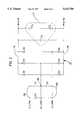
- FIG. 3graphically illustrates the voltage prior to the motor cable with and without the circuit of the present invention.
- FIG. 4is a graph similar to FIG. 3 showing the voltage applied to the controlled motor.
- Circuit 10is connected between an inverter 12 and an ac induction motor 14 adapted to operate on a load (not shown). Circuit 10 is electrically connected to motor 14 by a conductive cable 16.
- the distributed capacitances and inductances of cable 16are modeled as capacitors C1, C2 and C3 connected in a delta configuration between series connected inductors L1 and L4 at node 18, between L2 and L5 at node 20 and between L3 and L6 at node 22.
- Cable 16is connected to circuit 10 output contactor 24 via modeled lines 30, 32, 34.
- the inputs to limiting circuit 10are provided from output lines 36, 38 and 40 of inverter 12. These inverter output lines are connected to limiting circuit input lines 54, 56 and 58, respectively.
- Inverter output line 36is connected to inverter line 42 intermediate a pair of switches 42a and 42b.
- Inverter outputs 38 and 40are connected in a similar fashion to inverter lines 44 and 46, respectively.
- Switches 42a, 44a, 46a, 42b, 44b, 46bare preferably power switching elements such as insulated gate bipolar transistors (IGBTs) which are alternately switched on and off by firing signals from a separately connected element such as a micro-processor based pulse width modulator (not shown).
- a dc voltageis supplied across bus lines 48 and 50 via a voltage source 52.
- Inverter 12is thus adapted to convert dc power applied by power supply 52 to polyphase alternating current necessary to power motor 14.
- inverter output lines 36, 38, 40would be directly coupled to cable lines 30, 32, 34.
- this conventional configurationhas several inherent disadvantages, the most notable of which is a high voltage rise rate and peak voltage to the distributed capacitances and inductances of cable 16, as modeled in FIG. 1. This not only adversely affects motor 14 but also limits the length of cable 16.
- Circuit 10counteracts such effects and raises cable length limits by limiting the rate of rise of voltage at the cable input and clamping positive voltage levels and returning trapped energy back onto dc bus lines 48 and 50.
- Circuit 10receives inputs on lines 54, 56 and 58 from inverter outputs 36, 38 and 40. Circuit 10 also includes output lines 60 and 62 connected to inverter 12 at nodes 44a and 44b, or the junctions at which line 44 joins bus lines 48 and 50, respectively.
- Input signals received on input lines 54, 56, 58are passed in series through a corresponding inductor L7, L8, L9.
- Inductor L7is connected at node 64 to parallel capacitors C4 and C5.
- Inductor L8is connected at node 66 to parallel capacitors C4 and C6 and L9 at node 68 to C6 and C5, capacitors C4, C5 and C6 being connected in a delta configuration.
- Each of nodes 64, 66, 68is electrically connected to an output of a fast recovery three-phase diode bridge rectifier 70.
- Rectifier 70produces dc output signals to lines 60 and 62 and therefore connected nodes 49 and 51.
- Lines 60 and 62each include a resistor, R1 and R2 respectively, having a capacitor C7 connected therebetween.
- FIG. 2illustrates limiting circuit 10, and in particular rectifier 70, in additional detail. As shown therein the input to rectifier 70 comes from nodes 64, 66 and 68 with capacitors C4, C5 and C6 connected therebetween.
- Node 64is electrically coupled to line 72 through diode D1 and to line 74 through diode D2.
- node 66connects to line 72 through diode D3 and to line 74 through diode D4.
- node 68is coupled to line 72 through diode D5 and to line 74 through diode D6.
- Lines 72 and 74provide dc current to resistors R1 and R2 with capacitor C7 connected therebetween.
- Capacitor C7preferably includes a set of three capacitors C7 1 , C7 2 , and C7 3 interconnected as shown in FIG. 2.
- Capacitor C7 1in this exemplary embodiment, preferably having a capacitance of about 0.1 microfarads provides a path for high frequency currents, thus controlling the peak voltage which is clamped by the capacitors and rectifier bridge.
- Capacitors C7 2 and C7 3are electrolytic capacitors which do not have the high frequency characteristics necessary to allow operation absent C7 1 but which, in series, have a voltage rating higher than can be normally attained with a single commercially available capacitor.
- the capacitances of C7 2 and C7 3are preferably chosen so as to allow motor current flowing through inductors L7, L8 and L9 to be absorbed when output contactor 24 is suddenly opened. If these capacitors are not properly sized, the voltage at the output of rectifier 70 would increase to a point wherein diodes DI-D6 may fail.
- Curve 80represents the voltage which would be seen directly from inverter 12, without the benefit of limiting circuit 10.
- Curve 82conversely shows the voltage output from limiting circuit 10.
- Curve 80includes three main segments, an increasing segment 80a, a peak 80b and a leveled off portion 80c. As illustrated in the figure, curve segment 80a has a fairly steep slope, indicative of a sharp voltage rise rate, up to and exceeding 15,000 volts/ ⁇ sec.
- segment 82acorresponding to the signal as conditioned by limiting circuit 10
- Curve 82has a peak voltage 82b slightly above that of 80b, due to the voltage drop in R1 and R2 causing the voltage on C7 to exceed the dc bus voltage 52, but then levels off after a brief oscillation at 82c to voltage 82d.
- FIG. 4plots the voltage applied to motor 14, further taking into consideration the distributed capacitances and inductances inherent in cable 16.
- Curve 84illustrates this voltage without benefit of limiting circuit 10 and curve 86 with circuit 10.
- curve 86substantially mirrors curve 84 but on a more gradual and narrower scale. While voltage peaks at point 84b, after a sharp increase along curve portion 84a, at up to twice the inverter voltage, the peak voltage at 86b is only slightly more than one times the inverter voltage. In addition, the applied voltage is more stable.
- the present limiting circuitreduces the risk of detrimental high voltage peaks and rise rates to an inverter-driven induction motor.
- the circuitis simple, inexpensive and readily implemented in existing motor/drive systems.
Landscapes
- Engineering & Computer Science (AREA)
- Power Engineering (AREA)
- Inverter Devices (AREA)
- Control Of Ac Motors In General (AREA)
Abstract
Description
______________________________________ Resistors Capacitors Inductors Diodes ______________________________________ R1 20Ω C4 10,000pF L7 130μH D1 BY329-1200 R2 20Ω C5 10,000pF L8 130μH D2 BY329-1200 (Rl and C6 10,000pF L9 130μH D3 BY329-1200 R2 are C7.sub.1.1μF D4 BY329-1200 100 Watt) C7.sub.2 120μF D5 BY329-1200 C7.sub.3 120μF D6 BY329-1200 ______________________________________
Claims (7)
Priority Applications (3)
| Application Number | Priority Date | Filing Date | Title |
|---|---|---|---|
| US08/374,013US5633790A (en) | 1995-01-18 | 1995-01-18 | DV/DT limiting of inverter output voltage |
| GB9600935AGB2297208B (en) | 1995-01-18 | 1996-01-17 | DV/DT Limiting of inverter output voltage |
| CA002167546ACA2167546C (en) | 1995-01-18 | 1996-01-18 | Dv/dt limiting of inverter output voltage |
Applications Claiming Priority (1)
| Application Number | Priority Date | Filing Date | Title |
|---|---|---|---|
| US08/374,013US5633790A (en) | 1995-01-18 | 1995-01-18 | DV/DT limiting of inverter output voltage |
Publications (1)
| Publication Number | Publication Date |
|---|---|
| US5633790Atrue US5633790A (en) | 1997-05-27 |
Family
ID=23474872
Family Applications (1)
| Application Number | Title | Priority Date | Filing Date |
|---|---|---|---|
| US08/374,013Expired - LifetimeUS5633790A (en) | 1995-01-18 | 1995-01-18 | DV/DT limiting of inverter output voltage |
Country Status (3)
| Country | Link |
|---|---|
| US (1) | US5633790A (en) |
| CA (1) | CA2167546C (en) |
| GB (1) | GB2297208B (en) |
Cited By (23)
| Publication number | Priority date | Publication date | Assignee | Title |
|---|---|---|---|---|
| US5808882A (en)* | 1995-12-28 | 1998-09-15 | Kabushiki Kaisha Toshiba | Three-phase bridge rectifier |
| US20080007197A1 (en)* | 2006-06-26 | 2008-01-10 | Hitachi, Ltd. | Inverter-driven rotating machine system, rotating machine and inverter used in the same and electric vehicle using the same |
| US7375890B2 (en) | 2002-09-12 | 2008-05-20 | Cyvera Corporation | Method of manufacturing of a diffraction grating-based optical identification element |
| US20080150462A1 (en)* | 2006-12-21 | 2008-06-26 | Abb Oy | Method and arrangement in connection with motor fed with frequency converter provided with intermediate voltage circuit |
| US7433123B2 (en) | 2004-02-19 | 2008-10-07 | Illumina, Inc. | Optical identification element having non-waveguide photosensitive substrate with diffraction grating therein |
| US7441703B2 (en) | 2002-08-20 | 2008-10-28 | Illumina, Inc. | Optical reader for diffraction grating-based encoded optical identification elements |
| US7508608B2 (en) | 2004-11-17 | 2009-03-24 | Illumina, Inc. | Lithographically fabricated holographic optical identification element |
| US7602952B2 (en) | 2004-11-16 | 2009-10-13 | Illumina, Inc. | Scanner having spatial light modulator |
| US7604173B2 (en) | 2004-11-16 | 2009-10-20 | Illumina, Inc. | Holographically encoded elements for microarray and other tagging labeling applications, and method and apparatus for making and reading the same |
| US7619819B2 (en) | 2002-08-20 | 2009-11-17 | Illumina, Inc. | Method and apparatus for drug product tracking using encoded optical identification elements |
| US7623624B2 (en) | 2005-11-22 | 2009-11-24 | Illumina, Inc. | Method and apparatus for labeling using optical identification elements characterized by X-ray diffraction |
| US7659983B2 (en) | 2003-01-22 | 2010-02-09 | Electronics And Telecommunications Resarch Institute | Hybrid random bead/chip based microarray |
| US7872804B2 (en) | 2002-08-20 | 2011-01-18 | Illumina, Inc. | Encoded particle having a grating with variations in the refractive index |
| US7901630B2 (en) | 2002-08-20 | 2011-03-08 | Illumina, Inc. | Diffraction grating-based encoded microparticle assay stick |
| US7923260B2 (en) | 2002-08-20 | 2011-04-12 | Illumina, Inc. | Method of reading encoded particles |
| US20110129368A1 (en)* | 2009-11-30 | 2011-06-02 | Franklin Electric Company, Inc. | Variable speed drive system |
| US8081792B2 (en) | 2003-08-20 | 2011-12-20 | Illumina, Inc. | Fourier scattering methods for encoding microbeads and methods and apparatus for reading the same |
| US20130114312A1 (en)* | 2011-11-04 | 2013-05-09 | Zbb Energy Corporation | System and Method for Power Conversion for Renewable Energy Sources |
| US8470605B2 (en) | 2002-09-12 | 2013-06-25 | Illumina, Inc. | Optical reader for reading encoded microparticles |
| US8664903B2 (en) | 2011-06-27 | 2014-03-04 | Franklin Electric Company, Inc. | Adaptive flux control drive |
| JP2020005364A (en)* | 2018-06-26 | 2020-01-09 | 富士電機株式会社 | Motor overvoltage protection device, and power conversion apparatus and multi-phase motor driving apparatus using the same |
| CN110890848A (en)* | 2018-09-07 | 2020-03-17 | 丹佛斯电力电子有限公司 | Method for regulating an inverter connected to an electric machine via a du/dt filter |
| EP4143956A4 (en)* | 2020-04-29 | 2024-06-05 | BAE Systems Controls Inc. | Ac drive dv/dt filter using reverse recovery charge of diodes |
Families Citing this family (4)
| Publication number | Priority date | Publication date | Assignee | Title |
|---|---|---|---|---|
| FI119669B (en) | 2007-06-20 | 2009-01-30 | Vacon Oyj | Limitation of a voltage pulse |
| GB2460633B (en)* | 2008-06-02 | 2012-06-20 | Jason David Boull | Whipper motor surge suppressor for vending machines |
| EP3001553A1 (en)* | 2014-09-25 | 2016-03-30 | ABB Oy | Electric assembly |
| DE102014115139A1 (en)* | 2014-10-17 | 2016-04-21 | TRUMPF Hüttinger GmbH + Co. KG | Method and device for overvoltage limiting of an AC voltage generating arrangement |
Citations (4)
| Publication number | Priority date | Publication date | Assignee | Title |
|---|---|---|---|---|
| GB2189952A (en)* | 1986-04-30 | 1987-11-04 | Westinghouse Electric Corp | Multi-function control system for an induction motor drive |
| US4843515A (en)* | 1987-04-20 | 1989-06-27 | Keytek Instrument Corp. | Surge undershoot eliminator |
| US5461556A (en)* | 1991-10-22 | 1995-10-24 | Hitachi, Ltd. | Power converter |
| US5483140A (en)* | 1993-10-01 | 1996-01-09 | Wisconsin Alumni Research Foundation | Thyristor based DC link current source power conversion system for motor driven operation |
- 1995
- 1995-01-18USUS08/374,013patent/US5633790A/ennot_activeExpired - Lifetime
- 1996
- 1996-01-17GBGB9600935Apatent/GB2297208B/ennot_activeExpired - Fee Related
- 1996-01-18CACA002167546Apatent/CA2167546C/ennot_activeExpired - Fee Related
Patent Citations (4)
| Publication number | Priority date | Publication date | Assignee | Title |
|---|---|---|---|---|
| GB2189952A (en)* | 1986-04-30 | 1987-11-04 | Westinghouse Electric Corp | Multi-function control system for an induction motor drive |
| US4843515A (en)* | 1987-04-20 | 1989-06-27 | Keytek Instrument Corp. | Surge undershoot eliminator |
| US5461556A (en)* | 1991-10-22 | 1995-10-24 | Hitachi, Ltd. | Power converter |
| US5483140A (en)* | 1993-10-01 | 1996-01-09 | Wisconsin Alumni Research Foundation | Thyristor based DC link current source power conversion system for motor driven operation |
Cited By (31)
| Publication number | Priority date | Publication date | Assignee | Title |
|---|---|---|---|---|
| US5808882A (en)* | 1995-12-28 | 1998-09-15 | Kabushiki Kaisha Toshiba | Three-phase bridge rectifier |
| US7923260B2 (en) | 2002-08-20 | 2011-04-12 | Illumina, Inc. | Method of reading encoded particles |
| US7441703B2 (en) | 2002-08-20 | 2008-10-28 | Illumina, Inc. | Optical reader for diffraction grating-based encoded optical identification elements |
| US7901630B2 (en) | 2002-08-20 | 2011-03-08 | Illumina, Inc. | Diffraction grating-based encoded microparticle assay stick |
| US7872804B2 (en) | 2002-08-20 | 2011-01-18 | Illumina, Inc. | Encoded particle having a grating with variations in the refractive index |
| US7619819B2 (en) | 2002-08-20 | 2009-11-17 | Illumina, Inc. | Method and apparatus for drug product tracking using encoded optical identification elements |
| US8470605B2 (en) | 2002-09-12 | 2013-06-25 | Illumina, Inc. | Optical reader for reading encoded microparticles |
| US7375890B2 (en) | 2002-09-12 | 2008-05-20 | Cyvera Corporation | Method of manufacturing of a diffraction grating-based optical identification element |
| US7898735B2 (en) | 2002-09-12 | 2011-03-01 | Illumina, Inc. | Methods and systems for writing an optical code within or on a fiber substrate |
| US7659983B2 (en) | 2003-01-22 | 2010-02-09 | Electronics And Telecommunications Resarch Institute | Hybrid random bead/chip based microarray |
| US8081792B2 (en) | 2003-08-20 | 2011-12-20 | Illumina, Inc. | Fourier scattering methods for encoding microbeads and methods and apparatus for reading the same |
| US7791802B2 (en) | 2004-02-19 | 2010-09-07 | Illumina, Inc. | Optical identification element having a non-waveguide substrate |
| US7433123B2 (en) | 2004-02-19 | 2008-10-07 | Illumina, Inc. | Optical identification element having non-waveguide photosensitive substrate with diffraction grating therein |
| US7604173B2 (en) | 2004-11-16 | 2009-10-20 | Illumina, Inc. | Holographically encoded elements for microarray and other tagging labeling applications, and method and apparatus for making and reading the same |
| US7602952B2 (en) | 2004-11-16 | 2009-10-13 | Illumina, Inc. | Scanner having spatial light modulator |
| US7796333B2 (en) | 2004-11-17 | 2010-09-14 | Illumina, Inc. | Encoded microparticles and a method for fabricating |
| US7508608B2 (en) | 2004-11-17 | 2009-03-24 | Illumina, Inc. | Lithographically fabricated holographic optical identification element |
| US7623624B2 (en) | 2005-11-22 | 2009-11-24 | Illumina, Inc. | Method and apparatus for labeling using optical identification elements characterized by X-ray diffraction |
| US20080007197A1 (en)* | 2006-06-26 | 2008-01-10 | Hitachi, Ltd. | Inverter-driven rotating machine system, rotating machine and inverter used in the same and electric vehicle using the same |
| US7764042B2 (en)* | 2006-06-26 | 2010-07-27 | Hitachi, Ltd. | Inverter-driven rotating machine system, rotating machine and inverter used in the same and electric vehicle using the same |
| US7733048B2 (en)* | 2006-12-21 | 2010-06-08 | Abb Oy | Method and arrangement in connection with motor fed with frequency converter provided with intermediate voltage circuit |
| US20080150462A1 (en)* | 2006-12-21 | 2008-06-26 | Abb Oy | Method and arrangement in connection with motor fed with frequency converter provided with intermediate voltage circuit |
| US20110129368A1 (en)* | 2009-11-30 | 2011-06-02 | Franklin Electric Company, Inc. | Variable speed drive system |
| US8760089B2 (en) | 2009-11-30 | 2014-06-24 | Franklin Electric Company, Inc. | Variable speed drive system |
| US8664903B2 (en) | 2011-06-27 | 2014-03-04 | Franklin Electric Company, Inc. | Adaptive flux control drive |
| US20130114312A1 (en)* | 2011-11-04 | 2013-05-09 | Zbb Energy Corporation | System and Method for Power Conversion for Renewable Energy Sources |
| US8958218B2 (en)* | 2011-11-04 | 2015-02-17 | Zbb Energy Corporation | System and method for power conversion for renewable energy sources |
| JP2020005364A (en)* | 2018-06-26 | 2020-01-09 | 富士電機株式会社 | Motor overvoltage protection device, and power conversion apparatus and multi-phase motor driving apparatus using the same |
| CN110890848A (en)* | 2018-09-07 | 2020-03-17 | 丹佛斯电力电子有限公司 | Method for regulating an inverter connected to an electric machine via a du/dt filter |
| CN110890848B (en)* | 2018-09-07 | 2023-01-10 | 丹佛斯电力电子有限公司 | Method for regulating an inverter connected to an electric machine via a du/dt filter |
| EP4143956A4 (en)* | 2020-04-29 | 2024-06-05 | BAE Systems Controls Inc. | Ac drive dv/dt filter using reverse recovery charge of diodes |
Also Published As
| Publication number | Publication date |
|---|---|
| CA2167546A1 (en) | 1996-07-19 |
| GB9600935D0 (en) | 1996-03-20 |
| CA2167546C (en) | 2000-02-22 |
| GB2297208A (en) | 1996-07-24 |
| GB2297208B (en) | 1999-04-14 |
Similar Documents
| Publication | Publication Date | Title |
|---|---|---|
| US5633790A (en) | DV/DT limiting of inverter output voltage | |
| US4833584A (en) | Quasi-resonant current mode static power conversion method and apparatus | |
| US4730242A (en) | Static power conversion and apparatus having essentially zero switching losses | |
| US5684688A (en) | Soft switching three-level inverter | |
| US5047910A (en) | Ideal sinusoidal voltage waveform synthesis control system | |
| US5914590A (en) | Electrical power regulator | |
| US7394627B2 (en) | Frequency converter having an intermediate circuit without any capacitors | |
| US5936856A (en) | Method and apparatus for active common-mode voltage compensation in induction motor systems | |
| US5835371A (en) | Bridge type power converter | |
| EP0473192B2 (en) | A circuit for reducing resonance voltage | |
| US4884185A (en) | Pulse width modulation converter | |
| WO2019021159A1 (en) | Switch control circuit for a gate drive | |
| US5990658A (en) | Apparatus for controlling reflected voltage on motor supply lines | |
| US5130917A (en) | Power inverter snubber circuit | |
| JP4673648B2 (en) | Converter control apparatus and method, and converter and electric apparatus having the apparatus | |
| HU226738B1 (en) | Method for processing pwm waves | |
| WO1991009454A1 (en) | Dc-link ripple reduction circuit | |
| JP4132316B2 (en) | Control method of three-phase voltage source inverter | |
| JPH11127540A (en) | Method of supplying reactive power to AC grid system and inverter used in this method | |
| CN111130376B (en) | Three-phase pulse width modulation rectifying circuit and pre-charging method thereof | |
| Chen et al. | Loss-less and cost-effective cable terminator topologies with no voltage overshoot | |
| US4404512A (en) | Motor drive circuit | |
| CN110429803A (en) | Driving circuit and inverter | |
| EP0469003A1 (en) | Circuits with switching protection and parts therefor | |
| JP3104733B2 (en) | Bridge type inverter device |
Legal Events
| Date | Code | Title | Description |
|---|---|---|---|
| AS | Assignment | Owner name:EATON CORPORATION, OHIO Free format text:ASSIGNMENT OF ASSIGNORS INTEREST;ASSIGNORS:GRITTER, DAVID J.;REICHARD, JEFFREY A.;REEL/FRAME:007305/0340;SIGNING DATES FROM 19941208 TO 19950105 | |
| FEPP | Fee payment procedure | Free format text:PAYOR NUMBER ASSIGNED (ORIGINAL EVENT CODE: ASPN); ENTITY STATUS OF PATENT OWNER: LARGE ENTITY | |
| STCF | Information on status: patent grant | Free format text:PATENTED CASE | |
| FPAY | Fee payment | Year of fee payment:4 | |
| AS | Assignment | Owner name:CAMP, OHIO Free format text:ASSIGNMENT OF ASSIGNORS INTEREST;ASSIGNOR:EATON CORPORATION;REEL/FRAME:014108/0090 Effective date:20030523 | |
| FEPP | Fee payment procedure | Free format text:PAT HOLDER CLAIMS SMALL ENTITY STATUS, ENTITY STATUS SET TO SMALL (ORIGINAL EVENT CODE: LTOS); ENTITY STATUS OF PATENT OWNER: LARGE ENTITY | |
| FPAY | Fee payment | Year of fee payment:8 | |
| FPAY | Fee payment | Year of fee payment:12 | |
| FEPP | Fee payment procedure | Free format text:PAT HOLDER NO LONGER CLAIMS SMALL ENTITY STATUS, ENTITY STATUS SET TO UNDISCOUNTED (ORIGINAL EVENT CODE: STOL); ENTITY STATUS OF PATENT OWNER: LARGE ENTITY | |
| SULP | Surcharge for late payment | ||
| FEPP | Fee payment procedure | Free format text:ENTITY STATUS SET TO UNDISCOUNTED (ORIGINAL EVENT CODE: BIG.); ENTITY STATUS OF PATENT OWNER: LARGE ENTITY | |
| FEPP | Fee payment procedure | Free format text:PETITION RELATED TO MAINTENANCE FEES GRANTED (ORIGINAL EVENT CODE: PTGR); ENTITY STATUS OF PATENT OWNER: LARGE ENTITY |