US5633189A - Method of making metal to metal antifuse - Google Patents
Method of making metal to metal antifuseDownload PDFInfo
- Publication number
- US5633189A US5633189AUS08/425,122US42512295AUS5633189AUS 5633189 AUS5633189 AUS 5633189AUS 42512295 AUS42512295 AUS 42512295AUS 5633189 AUS5633189 AUS 5633189A
- Authority
- US
- United States
- Prior art keywords
- antifuse
- layer
- barrier metal
- over
- metal layer
- Prior art date
- Legal status (The legal status is an assumption and is not a legal conclusion. Google has not performed a legal analysis and makes no representation as to the accuracy of the status listed.)
- Expired - Lifetime
Links
Images


Classifications
- H—ELECTRICITY
- H01—ELECTRIC ELEMENTS
- H01L—SEMICONDUCTOR DEVICES NOT COVERED BY CLASS H10
- H01L23/00—Details of semiconductor or other solid state devices
- H01L23/52—Arrangements for conducting electric current within the device in operation from one component to another, i.e. interconnections, e.g. wires, lead frames
- H01L23/522—Arrangements for conducting electric current within the device in operation from one component to another, i.e. interconnections, e.g. wires, lead frames including external interconnections consisting of a multilayer structure of conductive and insulating layers inseparably formed on the semiconductor body
- H01L23/525—Arrangements for conducting electric current within the device in operation from one component to another, i.e. interconnections, e.g. wires, lead frames including external interconnections consisting of a multilayer structure of conductive and insulating layers inseparably formed on the semiconductor body with adaptable interconnections
- H01L23/5252—Arrangements for conducting electric current within the device in operation from one component to another, i.e. interconnections, e.g. wires, lead frames including external interconnections consisting of a multilayer structure of conductive and insulating layers inseparably formed on the semiconductor body with adaptable interconnections comprising anti-fuses, i.e. connections having their state changed from non-conductive to conductive
- H—ELECTRICITY
- H01—ELECTRIC ELEMENTS
- H01L—SEMICONDUCTOR DEVICES NOT COVERED BY CLASS H10
- H01L2924/00—Indexing scheme for arrangements or methods for connecting or disconnecting semiconductor or solid-state bodies as covered by H01L24/00
- H01L2924/0001—Technical content checked by a classifier
- H01L2924/0002—Not covered by any one of groups H01L24/00, H01L24/00 and H01L2224/00
Definitions
- the present inventionis directed to a metal-to-metal antifuse structure for use in microcircuit structures such as Field Programmable Gate Arrays (FPGAs) and the like. More particularly, the antifuse structure of the present invention comprises an antifuse cell opening in which is deposited a barrier metal by means of collimated sputtering deposition over which is deposited the antifuse material layer and then another barrier metal layer.
- the resulting structureis advantageous in that it can be fabricated with standard CMOS process techniques plus the addition of collimated sputtering and it provides a device having a low capacitance antifuse operable at higher speeds.
- Prior art metal-to-metal antifuse structuresgenerally comprise a planar bottom electrode on top of which is disposed a planar barrier metal layer.
- An interlayer dielectric layer (ILD)is disposed over the bottom electrode structure and an antifuse cell opening is formed in the ILD to expose the bottom electrode.
- An antifuse material layermay then be deposited in the antifuse cell opening (or "via") and appropriate layers deposited over the antifuse material layer.
- the antifuse structure of the present inventionincludes a bottom planarized electrode, an ILD disposed over the bottom electrode, an antifuse cell opening in and through the ILD exposing the bottom electrode, a first barrier metal layer disposed by means of collimated sputter deposition in the antifuse cell opening to form a layer of uniform thickness existing only within the antifuse cell opening in order to protect the antifuse material layer from diffusion from the bottom electrode and to form an effective bottom electrode of reduced area, hence reducing the capacitance of the device, an antifuse material layer disposed in the antifuse cell-opening and over the first barrier metal layer, a second barrier metal layer disposed over the antifuse material layer and optionally formed by collimated sputter deposition, and a top electrode disposed over the second barrier metal layer.
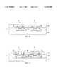
- FIGS. 1-9are diagrams showing progressive stages of construction of the metal-to-metal antifuse structure according to the present invention.
- FIG. 10is a diagram showing the completed metal-to-metal antifuse structure according to the present invention.
- FIG. 11is a diagram showing an alternative embodiment of the completed metal-to-metal antifuse structure according to the present invention.
- the present inventionis directed to an improved metal-to-metal antifuse structure utilizing collimated sputter deposition to form at least the first barrier layer which provides an easily manufactured device using standard CMOS process steps in addition to collimated sputter deposition.
- An advantage of the novel structureis reduced capacitance with reduced capacitance over prior art metal-to-metal antifuse structures.
- FIG. 1depicts a substrate 10 on which has been formed a pair of bottom electrodes 12 which will form the bottom antifuse electrode.
- the substrate 10may be any insulating portion of a microcircuit or semiconductor structure.
- Bottom electrodes 12are preferably aluminum of thickness in the range of 3000 ⁇ -10000 ⁇ with 5000 ⁇ presently preferred.
- Bottom electrodes 12can also be any standard metallization compatible with standard CMOS processes.
- an interlayer dielectric layer (ILD) 14preferably of oxide of thickness in the range of 3000 ⁇ -10000 ⁇ with 5000 ⁇ presently preferred.
- ILDinterlayer dielectric layer
- FIG. 3shows the structure after stripping the resist layer 16.
- a first barrier metal layer 20/20ais formed by collimated sputter deposition of a barrier metal material such as tungsten (W), titanium-tungsten (TiW), titanium-tungsten nitride (TiWN), titanium nitride (TIN), titanium (Ti), tungsten silicide (WSix), and combinations of the foregoing.
- barrier metal layer 20/20ais formed of TiN of thickness in the range of 1000 ⁇ -3000 ⁇ with 2000 ⁇ presently preferred.
- barrier metal layer 20is disposed over ILD 14 and barrier metal layer 20a is disposed directly over and in contact with bottom electrodes 12 within antifuse cell openings 18.
- a photoresist layer 22 of thickness in the range of 0.4-0.7 ⁇ mis spun on and then uniformly blanket etched back until ILD 14 is exposed to yield the structure of FIG. 6. Then the resist layer 22a remaining (FIG. 6) is stripped using conventional resist stripping techniques to yield the result shown in FIG. 7--a flat barrier metal layer 20a (Via 18 is preferably round when looking down on it).
- Antifuse material layer 24is deposited over first barrier metal layer 20a.
- Antifuse material layer 24is preferably formed of a conventional nitride-amorphous silicon-nitride sandwich where the first (lower) nitride layer is preferably of thickness in the range of 70 ⁇ -200 ⁇ with 100 ⁇ presently preferred; the amorphous silicon layer is preferably of thickness in the range of 300 ⁇ -1000 ⁇ with 500 ⁇ presently preferred; and the second (upper) nitride layer is preferably of thickness in the range of 70 ⁇ -200 ⁇ with 100 ⁇ presently preferred.
- Over antifuse material layer 24is preferably deposited second barrier metal layer 26 which is preferably formed either by collimated sputter deposition or by a blanket deposit of a barrier metal material such as W, TiW, TiWN, TiN, Ti, WSix, and combinations of the foregoing.
- second barrier metal layer 26is formed of TiN of thickness in the range of 1000 ⁇ -3000 ⁇ with 2000 ⁇ presently preferred.
- top electrode metallization layer 28is formed over second barrier layer 26.
- the benefits of this novel structureinclude its full compatibility with existing standard CMOS processes and particularly its compatibility with the standard CMOS metallization and planarization.
- Fuse capacitanceis significantly reduced by the relatively smaller size of the first barrier metal layer versus the much larger size of the bottom electrode.
- Better step coverageis possible through the improved conformality for the antifuse material layer provided by the structure because the effective antifuse via depth is shallower due to the presence of the first barrier metal layer 20a within antifuse cell openings 18.
- a wide choice of barrier metalsare available since the structure described imposes less restriction on the choice of a barrier material.
- spacers 30, 32, 34 and 36may be added to further improve the performance of the structure as follows.
- Spacers 34 and 36improve the ability of antifuse material layer 24 to conform to the shape of the bottom of antifuse cell opening 18.
- Spacers 30 and 32help to isolate the aluminum in layer 28 from antifuse material layer 24 thus reducing side diffusion.
- Spacers 30, 32, 34 and 36may all be constructed of silicon oxide, silicon nitride and/or amorphous silicon as is well known to those of ordinary skill in the art.
- Spacers 34 and 36reduce the capacitance of the antifuse cell because they reduce the exposed area of bottom barrier metal layer 20a.
Landscapes
- Physics & Mathematics (AREA)
- Condensed Matter Physics & Semiconductors (AREA)
- General Physics & Mathematics (AREA)
- Engineering & Computer Science (AREA)
- Computer Hardware Design (AREA)
- Microelectronics & Electronic Packaging (AREA)
- Power Engineering (AREA)
- Design And Manufacture Of Integrated Circuits (AREA)
Abstract
Description
Claims (4)
Priority Applications (1)
| Application Number | Priority Date | Filing Date | Title |
|---|---|---|---|
| US08/425,122US5633189A (en) | 1994-08-01 | 1995-04-18 | Method of making metal to metal antifuse |
Applications Claiming Priority (4)
| Application Number | Priority Date | Filing Date | Title |
|---|---|---|---|
| US08/284,054US5614756A (en) | 1990-04-12 | 1994-08-01 | Metal-to-metal antifuse with conductive |
| US08/319,170US5541441A (en) | 1994-10-06 | 1994-10-06 | Metal to metal antifuse |
| US08/328,247US5543656A (en) | 1990-04-12 | 1994-10-24 | Metal to metal antifuse |
| US08/425,122US5633189A (en) | 1994-08-01 | 1995-04-18 | Method of making metal to metal antifuse |
Related Parent Applications (1)
| Application Number | Title | Priority Date | Filing Date |
|---|---|---|---|
| US08/328,247DivisionUS5543656A (en) | 1990-04-12 | 1994-10-24 | Metal to metal antifuse |
Publications (1)
| Publication Number | Publication Date |
|---|---|
| US5633189Atrue US5633189A (en) | 1997-05-27 |
Family
ID=27403443
Family Applications (1)
| Application Number | Title | Priority Date | Filing Date |
|---|---|---|---|
| US08/425,122Expired - LifetimeUS5633189A (en) | 1994-08-01 | 1995-04-18 | Method of making metal to metal antifuse |
Country Status (1)
| Country | Link |
|---|---|
| US (1) | US5633189A (en) |
Cited By (14)
| Publication number | Priority date | Publication date | Assignee | Title |
|---|---|---|---|---|
| US5739047A (en)* | 1996-06-17 | 1998-04-14 | Winbond Electronics Corporation | Method of fabricating a voidless IC electrical plug |
| US5856213A (en)* | 1996-07-25 | 1999-01-05 | Vlsi Technology, Inc. | Method of fabricating a programmable function system block using two masks and a sacrificial oxide layer between the bottom metal and an amorphous silicon antifuse structure |
| US5882997A (en)* | 1996-09-30 | 1999-03-16 | Vlsi Technology, Inc. | Method for making devices having thin load structures |
| US6190965B1 (en)* | 1997-12-19 | 2001-02-20 | Micron Technology, Inc. | Spacer patterned, high dielectric constant capacitor |
| DE10021098C1 (en)* | 2000-04-20 | 2001-09-20 | Infineon Technologies Ag | Production of conducting pathways on an integrated chip comprises applying a stacked dielectric layer, carrying out photolithography, etching, applying conducting material and removing, and applying an insulating layer |
| US6323536B1 (en) | 1996-08-26 | 2001-11-27 | Micron Technology, Inc. | Method and apparatus for forming a junctionless antifuse |
| WO2002067263A3 (en)* | 2001-02-19 | 2002-12-12 | Infineon Technologies Ag | Contact system comprising a dielectric antifuse for an ic-memory element and method for producing one such contact system |
| US6617262B2 (en)* | 2000-08-31 | 2003-09-09 | Micron Technology, Inc. | Sputtered insulating layer for wordline stacks |
| US6768185B2 (en)* | 2000-12-22 | 2004-07-27 | Matrix Semiconductor, Inc. | Formation of antifuse structure in a three dimensional memory |
| US20050082672A1 (en)* | 2003-10-17 | 2005-04-21 | Phoenix Precision Technology Corporation | Circuit barrier structure of semiconductor packaging substrate and method for fabricating the same |
| KR100574475B1 (en)* | 1998-12-30 | 2006-08-10 | 주식회사 하이닉스반도체 | Anti-Fuse Formation Method Using Metal Oxide Layer |
| US20060226544A1 (en)* | 2003-08-13 | 2006-10-12 | Shih-Ping Hsu | Semiconductor package substrate having contact pad protective layer formed thereon and method for fabricating the same |
| US8519509B2 (en) | 2010-04-16 | 2013-08-27 | Semiconductor Energy Laboratory Co., Ltd. | Semiconductor device and manufacturing method thereof |
| US10128184B2 (en) | 2015-07-01 | 2018-11-13 | Zhuhai Chuangfeixin Technology Co., Ltd. | Antifuse structure in via hole in interplayer dielectric |
Citations (42)
| Publication number | Priority date | Publication date | Assignee | Title |
|---|---|---|---|---|
| US3634929A (en)* | 1968-11-02 | 1972-01-18 | Tokyo Shibaura Electric Co | Method of manufacturing semiconductor integrated circuits |
| US3787822A (en)* | 1971-04-23 | 1974-01-22 | Philips Corp | Method of providing internal connections in a semiconductor device |
| JPS5998971A (en)* | 1982-11-30 | 1984-06-07 | 株式会社ナカ技術研究所 | Bearing structure of ceiling inspection port |
| EP0162529A1 (en)* | 1984-01-13 | 1985-11-27 | The British Petroleum Company p.l.c. | Amorphous or microcrystalline semiconductor memory device |
| US4561409A (en)* | 1984-10-26 | 1985-12-31 | Fernandez John J | Self-cleaning smog control filter for internal combustion engines |
| WO1987000969A1 (en)* | 1985-07-29 | 1987-02-12 | American Telephone & Telegraph Company | Three-level interconnection scheme for integrated circuits |
| WO1987002827A1 (en)* | 1985-10-29 | 1987-05-07 | 4C Electronics, Inc. | Programmable integrated crosspoint switch |
| US4748490A (en)* | 1985-08-01 | 1988-05-31 | Texas Instruments Incorporated | Deep polysilicon emitter antifuse memory cell |
| US4796075A (en)* | 1983-12-21 | 1989-01-03 | Advanced Micro Devices, Inc. | Fusible link structure for integrated circuits |
| US4822753A (en)* | 1988-05-09 | 1989-04-18 | Motorola, Inc. | Method for making a w/tin contact |
| EP0323078A2 (en)* | 1987-12-28 | 1989-07-05 | Actel Corporation | Electrically-programmable low-impedance anti-fuse element |
| US4847732A (en)* | 1983-09-15 | 1989-07-11 | Mosaic Systems, Inc. | Wafer and method of making same |
| US4870302A (en)* | 1984-03-12 | 1989-09-26 | Xilinx, Inc. | Configurable electrical circuit having configurable logic elements and configurable interconnects |
| DE3927033A1 (en)* | 1988-08-23 | 1990-03-01 | Seiko Epson Corp | SEMICONDUCTOR ELEMENT AND METHOD FOR THE PRODUCTION THEREOF |
| US4914055A (en)* | 1989-08-24 | 1990-04-03 | Advanced Micro Devices, Inc. | Semiconductor antifuse structure and method |
| US4933576A (en)* | 1988-05-13 | 1990-06-12 | Fujitsu Limited | Gate array device having macro cells for forming master and slave cells of master-slave flip-flop circuit |
| US4943538A (en)* | 1986-05-09 | 1990-07-24 | Actel Corporation | Programmable low impedance anti-fuse element |
| EP0452091A2 (en)* | 1990-04-12 | 1991-10-16 | Actel Corporation | Electrically programmable antifuse element and method of forming it |
| EP0455414A1 (en)* | 1990-04-30 | 1991-11-06 | AT&T Corp. | Integrated circuits having antifuses |
| US5095362A (en)* | 1990-10-23 | 1992-03-10 | Instant Circuit Corporation | Method for reducing resistance for programmed antifuse |
| US5100827A (en)* | 1991-02-27 | 1992-03-31 | At&T Bell Laboratories | Buried antifuse |
| US5120679A (en)* | 1991-06-04 | 1992-06-09 | Vlsi Technology, Inc. | Anti-fuse structures and methods for making same |
| WO1992013359A1 (en)* | 1991-01-17 | 1992-08-06 | Crosspoint Solutions, Inc. | An improved antifuse circuit structure for use in a field programmable gate array and method of manufacture thereof |
| WO1992020109A1 (en)* | 1991-05-03 | 1992-11-12 | Crosspoint Solutions, Inc. | A plug contact with antifuse and method of manufacture thereof |
| US5166556A (en)* | 1991-01-22 | 1992-11-24 | Myson Technology, Inc. | Programmable antifuse structure, process, logic cell and architecture for programmable integrated circuits |
| US5171715A (en)* | 1991-11-12 | 1992-12-15 | Actel Corporation | Process for fabricating electrically programmable antifuse element |
| WO1993003499A1 (en)* | 1991-07-26 | 1993-02-18 | Vlsi Technology, Inc. | Anti-fuse structures and methods for making same |
| US5191550A (en)* | 1989-11-30 | 1993-03-02 | Seiko Epson Corporation | Dual antifuse memory device |
| US5194759A (en)* | 1990-05-18 | 1993-03-16 | Actel Corporation | Methods for preventing disturbance of antifuses during programming |
| US5196724A (en)* | 1991-04-26 | 1993-03-23 | Quicklogic Corporation | Programmable interconnect structures and programmable integrated circuits |
| US5242851A (en)* | 1991-07-16 | 1993-09-07 | Samsung Semiconductor, Inc. | Programmable interconnect device and method of manufacturing same |
| US5248632A (en)* | 1992-09-29 | 1993-09-28 | Texas Instruments Incorporated | Method of forming an antifuse |
| US5272666A (en)* | 1991-10-18 | 1993-12-21 | Lattice Semiconductor Corporation | Programmable semiconductor antifuse structure and method of fabricating |
| US5272101A (en)* | 1990-04-12 | 1993-12-21 | Actel Corporation | Electrically programmable antifuse and fabrication processes |
| US5300456A (en)* | 1993-06-17 | 1994-04-05 | Texas Instruments Incorporated | Metal-to-metal antifuse structure |
| US5308795A (en)* | 1992-11-04 | 1994-05-03 | Actel Corporation | Above via metal-to-metal antifuse |
| US5313119A (en)* | 1991-03-18 | 1994-05-17 | Crosspoint Solutions, Inc. | Field programmable gate array |
| US5322812A (en)* | 1991-03-20 | 1994-06-21 | Crosspoint Solutions, Inc. | Improved method of fabricating antifuses in an integrated circuit device and resulting structure |
| US5329153A (en)* | 1992-04-10 | 1994-07-12 | Crosspoint Solutions, Inc. | Antifuse with nonstoichiometric tin layer and method of manufacture thereof |
| US5401675A (en)* | 1991-04-19 | 1995-03-28 | Lee; Pei-Ing P. | Method of depositing conductors in high aspect ratio apertures using a collimator |
| US5427981A (en)* | 1993-02-17 | 1995-06-27 | Hyundai Electronics Industries Co., Ltd. | Process for fabricating metal plus using metal silicide film |
| US5508220A (en)* | 1991-04-18 | 1996-04-16 | Actel Corporation | Method of forming antifuses having minimum areas |
- 1995
- 1995-04-18USUS08/425,122patent/US5633189A/ennot_activeExpired - Lifetime
Patent Citations (47)
| Publication number | Priority date | Publication date | Assignee | Title |
|---|---|---|---|---|
| US3634929A (en)* | 1968-11-02 | 1972-01-18 | Tokyo Shibaura Electric Co | Method of manufacturing semiconductor integrated circuits |
| US3787822A (en)* | 1971-04-23 | 1974-01-22 | Philips Corp | Method of providing internal connections in a semiconductor device |
| JPS5998971A (en)* | 1982-11-30 | 1984-06-07 | 株式会社ナカ技術研究所 | Bearing structure of ceiling inspection port |
| US4847732A (en)* | 1983-09-15 | 1989-07-11 | Mosaic Systems, Inc. | Wafer and method of making same |
| US4796075A (en)* | 1983-12-21 | 1989-01-03 | Advanced Micro Devices, Inc. | Fusible link structure for integrated circuits |
| EP0162529A1 (en)* | 1984-01-13 | 1985-11-27 | The British Petroleum Company p.l.c. | Amorphous or microcrystalline semiconductor memory device |
| US4870302A (en)* | 1984-03-12 | 1989-09-26 | Xilinx, Inc. | Configurable electrical circuit having configurable logic elements and configurable interconnects |
| US4561409A (en)* | 1984-10-26 | 1985-12-31 | Fernandez John J | Self-cleaning smog control filter for internal combustion engines |
| WO1987000969A1 (en)* | 1985-07-29 | 1987-02-12 | American Telephone & Telegraph Company | Three-level interconnection scheme for integrated circuits |
| US4748490A (en)* | 1985-08-01 | 1988-05-31 | Texas Instruments Incorporated | Deep polysilicon emitter antifuse memory cell |
| WO1987002827A1 (en)* | 1985-10-29 | 1987-05-07 | 4C Electronics, Inc. | Programmable integrated crosspoint switch |
| US4899205A (en)* | 1986-05-09 | 1990-02-06 | Actel Corporation | Electrically-programmable low-impedance anti-fuse element |
| US4943538A (en)* | 1986-05-09 | 1990-07-24 | Actel Corporation | Programmable low impedance anti-fuse element |
| EP0323078A2 (en)* | 1987-12-28 | 1989-07-05 | Actel Corporation | Electrically-programmable low-impedance anti-fuse element |
| US4822753A (en)* | 1988-05-09 | 1989-04-18 | Motorola, Inc. | Method for making a w/tin contact |
| US4933576A (en)* | 1988-05-13 | 1990-06-12 | Fujitsu Limited | Gate array device having macro cells for forming master and slave cells of master-slave flip-flop circuit |
| DE3927033A1 (en)* | 1988-08-23 | 1990-03-01 | Seiko Epson Corp | SEMICONDUCTOR ELEMENT AND METHOD FOR THE PRODUCTION THEREOF |
| US4914055A (en)* | 1989-08-24 | 1990-04-03 | Advanced Micro Devices, Inc. | Semiconductor antifuse structure and method |
| US5191550A (en)* | 1989-11-30 | 1993-03-02 | Seiko Epson Corporation | Dual antifuse memory device |
| US5272101A (en)* | 1990-04-12 | 1993-12-21 | Actel Corporation | Electrically programmable antifuse and fabrication processes |
| US5070384A (en)* | 1990-04-12 | 1991-12-03 | Actel Corporation | Electrically programmable antifuse element incorporating a dielectric and amorphous silicon interlayer |
| EP0452091A2 (en)* | 1990-04-12 | 1991-10-16 | Actel Corporation | Electrically programmable antifuse element and method of forming it |
| EP0455414A1 (en)* | 1990-04-30 | 1991-11-06 | AT&T Corp. | Integrated circuits having antifuses |
| US5194759A (en)* | 1990-05-18 | 1993-03-16 | Actel Corporation | Methods for preventing disturbance of antifuses during programming |
| US5095362A (en)* | 1990-10-23 | 1992-03-10 | Instant Circuit Corporation | Method for reducing resistance for programmed antifuse |
| WO1992013359A1 (en)* | 1991-01-17 | 1992-08-06 | Crosspoint Solutions, Inc. | An improved antifuse circuit structure for use in a field programmable gate array and method of manufacture thereof |
| US5166556A (en)* | 1991-01-22 | 1992-11-24 | Myson Technology, Inc. | Programmable antifuse structure, process, logic cell and architecture for programmable integrated circuits |
| US5100827A (en)* | 1991-02-27 | 1992-03-31 | At&T Bell Laboratories | Buried antifuse |
| US5313119A (en)* | 1991-03-18 | 1994-05-17 | Crosspoint Solutions, Inc. | Field programmable gate array |
| US5322812A (en)* | 1991-03-20 | 1994-06-21 | Crosspoint Solutions, Inc. | Improved method of fabricating antifuses in an integrated circuit device and resulting structure |
| US5508220A (en)* | 1991-04-18 | 1996-04-16 | Actel Corporation | Method of forming antifuses having minimum areas |
| US5401675A (en)* | 1991-04-19 | 1995-03-28 | Lee; Pei-Ing P. | Method of depositing conductors in high aspect ratio apertures using a collimator |
| US5196724A (en)* | 1991-04-26 | 1993-03-23 | Quicklogic Corporation | Programmable interconnect structures and programmable integrated circuits |
| US5233217A (en)* | 1991-05-03 | 1993-08-03 | Crosspoint Solutions | Plug contact with antifuse |
| WO1992020109A1 (en)* | 1991-05-03 | 1992-11-12 | Crosspoint Solutions, Inc. | A plug contact with antifuse and method of manufacture thereof |
| US5290734A (en)* | 1991-06-04 | 1994-03-01 | Vlsi Technology, Inc. | Method for making anti-fuse structures |
| US5120679A (en)* | 1991-06-04 | 1992-06-09 | Vlsi Technology, Inc. | Anti-fuse structures and methods for making same |
| US5242851A (en)* | 1991-07-16 | 1993-09-07 | Samsung Semiconductor, Inc. | Programmable interconnect device and method of manufacturing same |
| WO1993003499A1 (en)* | 1991-07-26 | 1993-02-18 | Vlsi Technology, Inc. | Anti-fuse structures and methods for making same |
| US5353246A (en)* | 1991-10-18 | 1994-10-04 | Lattice Semiconductor Corporation | Programmable semiconductor antifuse structure and method of fabricating |
| US5272666A (en)* | 1991-10-18 | 1993-12-21 | Lattice Semiconductor Corporation | Programmable semiconductor antifuse structure and method of fabricating |
| US5171715A (en)* | 1991-11-12 | 1992-12-15 | Actel Corporation | Process for fabricating electrically programmable antifuse element |
| US5329153A (en)* | 1992-04-10 | 1994-07-12 | Crosspoint Solutions, Inc. | Antifuse with nonstoichiometric tin layer and method of manufacture thereof |
| US5248632A (en)* | 1992-09-29 | 1993-09-28 | Texas Instruments Incorporated | Method of forming an antifuse |
| US5308795A (en)* | 1992-11-04 | 1994-05-03 | Actel Corporation | Above via metal-to-metal antifuse |
| US5427981A (en)* | 1993-02-17 | 1995-06-27 | Hyundai Electronics Industries Co., Ltd. | Process for fabricating metal plus using metal silicide film |
| US5300456A (en)* | 1993-06-17 | 1994-04-05 | Texas Instruments Incorporated | Metal-to-metal antifuse structure |
Non-Patent Citations (4)
| Title |
|---|
| Burns, G.P., "Titanium dioxide formed by rapid thermal oxidation", Journal of Applied Sciences, pp. 2095-2097, Nov. 04, 1988. |
| Burns, G.P., Titanium dioxide formed by rapid thermal oxidation , Journal of Applied Sciences, pp. 2095 2097, Nov. 04, 1988.* |
| Pauleau, "Interconnect Materials for VLSI Circuits", Apr., 1987, Solid State Technology, pp. 155-162. |
| Pauleau, Interconnect Materials for VLSI Circuits , Apr., 1987, Solid State Technology, pp. 155 162.* |
Cited By (30)
| Publication number | Priority date | Publication date | Assignee | Title |
|---|---|---|---|---|
| US5739047A (en)* | 1996-06-17 | 1998-04-14 | Winbond Electronics Corporation | Method of fabricating a voidless IC electrical plug |
| US5856213A (en)* | 1996-07-25 | 1999-01-05 | Vlsi Technology, Inc. | Method of fabricating a programmable function system block using two masks and a sacrificial oxide layer between the bottom metal and an amorphous silicon antifuse structure |
| US6444558B1 (en)* | 1996-08-26 | 2002-09-03 | Micron Technology, Inc. | Methods of forming and programming junctionless antifuses |
| US6525399B2 (en) | 1996-08-26 | 2003-02-25 | Micron Technology, Inc. | Junctionless antifuses and systems containing junctionless antifuses |
| US6323536B1 (en) | 1996-08-26 | 2001-11-27 | Micron Technology, Inc. | Method and apparatus for forming a junctionless antifuse |
| US5882997A (en)* | 1996-09-30 | 1999-03-16 | Vlsi Technology, Inc. | Method for making devices having thin load structures |
| US7388290B2 (en) | 1997-12-19 | 2008-06-17 | Micron Technology, Inc. | Spacer patterned, high dielectric constant capacitor and methods for fabricating the same |
| US6458654B1 (en) | 1997-12-19 | 2002-10-01 | Micron Technology, Inc. | Large surface area capacitor and methods for fabricating same |
| US7560799B2 (en) | 1997-12-19 | 2009-07-14 | Micron Technology, Inc. | Spacer patterned, high dielectric constant capacitor |
| US6566702B1 (en) | 1997-12-19 | 2003-05-20 | Micron Technology, Inc. | Spacer patterned, high dielectric constant capacitor |
| US20050059208A1 (en)* | 1997-12-19 | 2005-03-17 | Clampitt Darwin A. | Spacer patterned, high dielectric constant capacitor |
| US20030201486A1 (en)* | 1997-12-19 | 2003-10-30 | Clampitt Darwin A. | Spacer patterned, high dielectric constant capacitor |
| US6190965B1 (en)* | 1997-12-19 | 2001-02-20 | Micron Technology, Inc. | Spacer patterned, high dielectric constant capacitor |
| US6723602B2 (en) | 1997-12-19 | 2004-04-20 | Micron Technology, Inc. | Method for spacer patterned, high dielectric constant capacitor |
| US20070278552A1 (en)* | 1997-12-19 | 2007-12-06 | Micron Technology, Inc. | Spacer patterned, high dielectric constant capacitor |
| US6815754B2 (en) | 1997-12-19 | 2004-11-09 | Micron Technology, Inc. | Spacer patterned, high dielectric constant capacitor |
| KR100574475B1 (en)* | 1998-12-30 | 2006-08-10 | 주식회사 하이닉스반도체 | Anti-Fuse Formation Method Using Metal Oxide Layer |
| US6455435B1 (en) | 2000-04-20 | 2002-09-24 | Infineon Technologies Ag | Method for fabricating a wiring plane on a semiconductor chip with an antifuse |
| DE10021098C1 (en)* | 2000-04-20 | 2001-09-20 | Infineon Technologies Ag | Production of conducting pathways on an integrated chip comprises applying a stacked dielectric layer, carrying out photolithography, etching, applying conducting material and removing, and applying an insulating layer |
| US20040067629A1 (en)* | 2000-08-31 | 2004-04-08 | Micron Technology, Inc. | Sputtered insulating layer for wordline stacks |
| US6815372B2 (en) | 2000-08-31 | 2004-11-09 | Micron Technology, Inc. | Sputtered insulating layer for wordline stacks |
| US6617262B2 (en)* | 2000-08-31 | 2003-09-09 | Micron Technology, Inc. | Sputtered insulating layer for wordline stacks |
| US6768185B2 (en)* | 2000-12-22 | 2004-07-27 | Matrix Semiconductor, Inc. | Formation of antifuse structure in a three dimensional memory |
| WO2002067263A3 (en)* | 2001-02-19 | 2002-12-12 | Infineon Technologies Ag | Contact system comprising a dielectric antifuse for an ic-memory element and method for producing one such contact system |
| US20060226544A1 (en)* | 2003-08-13 | 2006-10-12 | Shih-Ping Hsu | Semiconductor package substrate having contact pad protective layer formed thereon and method for fabricating the same |
| US7485970B2 (en)* | 2003-08-13 | 2009-02-03 | Phoenix Precision Technology Corporation | Semiconductor package substrate having contact pad protective layer formed thereon |
| US20050082672A1 (en)* | 2003-10-17 | 2005-04-21 | Phoenix Precision Technology Corporation | Circuit barrier structure of semiconductor packaging substrate and method for fabricating the same |
| US7012019B2 (en)* | 2003-10-17 | 2006-03-14 | Phoenix Precision Technology Corporation | Circuit barrier structure of semiconductor packaging substrate and method for fabricating the same |
| US8519509B2 (en) | 2010-04-16 | 2013-08-27 | Semiconductor Energy Laboratory Co., Ltd. | Semiconductor device and manufacturing method thereof |
| US10128184B2 (en) | 2015-07-01 | 2018-11-13 | Zhuhai Chuangfeixin Technology Co., Ltd. | Antifuse structure in via hole in interplayer dielectric |
Similar Documents
| Publication | Publication Date | Title |
|---|---|---|
| US6001693A (en) | Method of making a metal to metal antifuse | |
| US5580814A (en) | Method for making a ferroelectric memory cell with a ferroelectric capacitor overlying a memory transistor | |
| US5387812A (en) | Electrically programmable antifuse having a metal to metal structure | |
| US5804500A (en) | Fabrication process for raised tungsten plug antifuse | |
| US5614756A (en) | Metal-to-metal antifuse with conductive | |
| US5633189A (en) | Method of making metal to metal antifuse | |
| US5807779A (en) | Method of making tungsten local interconnect using a silicon nitride capped self-aligned contact process | |
| US5466629A (en) | Process for fabricating ferroelectric integrated circuit | |
| US5780323A (en) | Fabrication method for metal-to-metal antifuses incorporating a tungsten via plug | |
| US6201726B1 (en) | Ferroelectric memory device structure useful for preventing hydrogen line degradation | |
| JP3715502B2 (en) | Semiconductor device and manufacturing method thereof | |
| US6448134B2 (en) | Method for fabricating semiconductor device | |
| JP2602219B2 (en) | Semiconductor storage device | |
| US6140231A (en) | Robust diffusion barrier for Cu metallization | |
| US5543656A (en) | Metal to metal antifuse | |
| KR0146861B1 (en) | Semiconductor device and method for fabricating the same, which have improved shielding rate by increased wiring layer | |
| KR0159450B1 (en) | An anti-fuse element | |
| US5557137A (en) | Voltage programmable link having reduced capacitance | |
| US5929505A (en) | Inter-metal-wiring antifuse device provided by self-alignment | |
| JP3594213B2 (en) | Method of forming connection portion and semiconductor chip | |
| JP3343251B2 (en) | Programmable interconnect structure, programmable integrated circuit and method of manufacturing the same | |
| US6040616A (en) | Device and method of forming a metal to metal capacitor within an integrated circuit | |
| JP2959412B2 (en) | Semiconductor memory device and method of manufacturing the same | |
| JP2000182989A (en) | Semiconductor device | |
| KR100358164B1 (en) | Method for forming ferroelectric memory device |
Legal Events
| Date | Code | Title | Description |
|---|---|---|---|
| STCF | Information on status: patent grant | Free format text:PATENTED CASE | |
| CC | Certificate of correction | ||
| FPAY | Fee payment | Year of fee payment:4 | |
| FPAY | Fee payment | Year of fee payment:8 | |
| FPAY | Fee payment | Year of fee payment:12 | |
| REMI | Maintenance fee reminder mailed | ||
| AS | Assignment | Owner name:MORGAN STANLEY & CO. INCORPORATED, NEW YORK Free format text:PATENT SECURITY AGREEMENT;ASSIGNORS:WHITE ELECTRONIC DESIGNS CORP.;ACTEL CORPORATION;MICROSEMI CORPORATION;REEL/FRAME:025783/0613 Effective date:20110111 | |
| AS | Assignment | Owner name:MICROSEMI FREQUENCY AND TIME CORPORATION, A DELAWA Free format text:RELEASE BY SECURED PARTY;ASSIGNOR:BANK OF AMERICA, N.A.;REEL/FRAME:037558/0711 Effective date:20160115 Owner name:MICROSEMI SEMICONDUCTOR (U.S.) INC., A DELAWARE CO Free format text:RELEASE BY SECURED PARTY;ASSIGNOR:BANK OF AMERICA, N.A.;REEL/FRAME:037558/0711 Effective date:20160115 Owner name:MICROSEMI CORP.-ANALOG MIXED SIGNAL GROUP, A DELAW Free format text:RELEASE BY SECURED PARTY;ASSIGNOR:BANK OF AMERICA, N.A.;REEL/FRAME:037558/0711 Effective date:20160115 Owner name:MICROSEMI CORPORATION, CALIFORNIA Free format text:RELEASE BY SECURED PARTY;ASSIGNOR:BANK OF AMERICA, N.A.;REEL/FRAME:037558/0711 Effective date:20160115 Owner name:MICROSEMI SOC CORP., A CALIFORNIA CORPORATION, CAL Free format text:RELEASE BY SECURED PARTY;ASSIGNOR:BANK OF AMERICA, N.A.;REEL/FRAME:037558/0711 Effective date:20160115 Owner name:MICROSEMI CORP.-MEMORY AND STORAGE SOLUTIONS (F/K/ Free format text:RELEASE BY SECURED PARTY;ASSIGNOR:BANK OF AMERICA, N.A.;REEL/FRAME:037558/0711 Effective date:20160115 Owner name:MICROSEMI COMMUNICATIONS, INC. (F/K/A VITESSE SEMI Free format text:RELEASE BY SECURED PARTY;ASSIGNOR:BANK OF AMERICA, N.A.;REEL/FRAME:037558/0711 Effective date:20160115 |