US5633180A - Method of forming P-type islands over P-type buried layer - Google Patents
Method of forming P-type islands over P-type buried layerDownload PDFInfo
- Publication number
- US5633180A US5633180AUS08/456,727US45672795AUS5633180AUS 5633180 AUS5633180 AUS 5633180AUS 45672795 AUS45672795 AUS 45672795AUS 5633180 AUS5633180 AUS 5633180A
- Authority
- US
- United States
- Prior art keywords
- layer
- sinker
- type
- collector
- layers
- Prior art date
- Legal status (The legal status is an assumption and is not a legal conclusion. Google has not performed a legal analysis and makes no representation as to the accuracy of the status listed.)
- Expired - Lifetime
Links
Images


Classifications
- H—ELECTRICITY
- H01—ELECTRIC ELEMENTS
- H01L—SEMICONDUCTOR DEVICES NOT COVERED BY CLASS H10
- H01L21/00—Processes or apparatus adapted for the manufacture or treatment of semiconductor or solid state devices or of parts thereof
- H01L21/70—Manufacture or treatment of devices consisting of a plurality of solid state components formed in or on a common substrate or of parts thereof; Manufacture of integrated circuit devices or of parts thereof
- H01L21/71—Manufacture of specific parts of devices defined in group H01L21/70
- H01L21/74—Making of localized buried regions, e.g. buried collector layers, internal connections substrate contacts
Definitions
- the present inventionrelates to the fabrication of semiconductor devices and more specifically, to a process for fabricating a vertical conductive region in a semiconductor device using plural epitaxial layers.
- a low resistivity regionwith the same conductivity type as the collector is placed under the collector.
- integrated circuitsinclude a collector contact that is on top of the transistor.
- the collector contact on top of the transistormay be linked to the buried layer with a further low resistivity region denoted a collector sinker.
- NPN transistorsare used in many integrated circuits because they have better electrical performance than PNP transistors, and because they are easier to fabricate.
- a common procedure for fabricating an NPN transistor in an integrated circuitis to form an N+ buried layer in the substrate by selective ion implantation, and to grow an N-type epitaxial layer on top of the buried layer that will serve as the collector of the transistor.
- An N+ collector sinkermay be formed by selectively implanting and diffusing N-type dopant into the epitaxial layer.
- the fabrication processis similar for complementary bipolar circuits where both NPN and PNP transistors are used, although extra steps may be needed for the PNP transistor.
- the extra stepstypically include the formation of a P+ buried layer and the P-type collector.
- a P+ collector sinkermay be omitted.
- a conventional fast vertical PNP transistor 10 in a complementary bipolar circuitmay contain a P-type vertical conductive region that includes a low resistance buried layer 12 within an N-type region of a substrate 14 that is contacted by a sinker 16 and a collector 18 extending through an N-type epitaxial layer 20.
- the breakdown voltage of a fast transistor operating in the GHz frequency rangeis about 10 volts or less, and the epitaxial layer 20 has a thickness of about 2.5 microns or less.
- the P-type collector 18 and P+ collector sinker 16may be formed in epitaxial layers of this thickness with a single implantation and appropriate diffusion. If, however, the breakdown voltage is to be larger, a thicker epitaxial layer will be needed. Epitaxial layers thicker than 2.5 microns may be too thick for a conventional low energy implanter (they do not have enough energy to implant the doping ions to the bottom of the layer), and high energy implanters (e.g., MeV) are needed. High energy implanters are expensive and also have depth limitations.
- FIG. 1is a vertical cross section of a portion of a conventional semiconductor device with a vertical conductive region.
- FIGS. 2A-2Care vertical cross sections illustrating an embodiment of the method of the present invention in various fabrication steps.
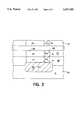
- FIG. 3is a vertical cross section of another embodiment of the present invention.
- FIG. 4is a vertical cross section of another embodiment of the present invention.
- a semiconductor device 22may be provided with a substrate 24 of a first conductivity type (N type is shown although the invention is not so limited).
- a buried layer 26 of the second conductivity type(P in this example) may be placed therein.
- a first layer 28 of the first conductivity typemay be grown on the substrate 24.
- the thickness T 1 of layer 28is desirably selected so that an implant of conventional energy (e.g., ion energy less than about 300 KeV) will allow the buried layer to diffuse upwards to join a downwardly implanted dopant.
- T 1may be from about 0.5 microns to about 2.5 microns, with the latter being preferred to reduce the number layers that will be needed to reach a desired height.
- a second N type epitaxial layer 32may be grown over the first layer 28.
- the thickness T 2 of the second layer 32is desirably selected so that conventional energy implants will extend to the surface of the first layer 28.
- T 2may be from about 0.5 microns to about 1.5 microns, with the latter being preferred to reduce the number layers that will be needed to reach a desired height.
- a second conventional implant of P type dopantmay be implanted into the second epitaxial layer 32 to form a further portion 34 of the vertical conductive region: that is, the vertical conductive region 30 is extended vertically to the top of the second layer 32.
- additional N type epitaxial layers L nmay be grown by repeating the steps for the second layer 32 described above. These steps may be repeated n times until the desired height T t of vertical conductive region 30 is achieved.
- T tmay be from 5 microns to 25 microns.
- FIG. 3illustrates another embodiment of the method of the present invention in which the vertical conductive region 30 includes a collector 36 and a sinker 38.
- the element numbers from FIG. 2have been maintained for ease of reference.
- a P type dopantmay be implanted into the first epitaxial layer 28 over the buried layer.
- Two selective implants with different doses of implanted ionsmay form a section of P+ sinker 38 and a section of a P- collector 36 that join with the buried layer 32 and extend to the top of the first epitaxial layer 28.
- the high conductivity sinker and the collectoreach form separate unitary structures that are juxtaposed and in contact.
Landscapes
- Engineering & Computer Science (AREA)
- Physics & Mathematics (AREA)
- Condensed Matter Physics & Semiconductors (AREA)
- General Physics & Mathematics (AREA)
- Manufacturing & Machinery (AREA)
- Computer Hardware Design (AREA)
- Microelectronics & Electronic Packaging (AREA)
- Power Engineering (AREA)
- Bipolar Transistors (AREA)
Abstract
Description
Claims (19)
Priority Applications (1)
| Application Number | Priority Date | Filing Date | Title |
|---|---|---|---|
| US08/456,727US5633180A (en) | 1995-06-01 | 1995-06-01 | Method of forming P-type islands over P-type buried layer |
Applications Claiming Priority (1)
| Application Number | Priority Date | Filing Date | Title |
|---|---|---|---|
| US08/456,727US5633180A (en) | 1995-06-01 | 1995-06-01 | Method of forming P-type islands over P-type buried layer |
Publications (1)
| Publication Number | Publication Date |
|---|---|
| US5633180Atrue US5633180A (en) | 1997-05-27 |
Family
ID=23813902
Family Applications (1)
| Application Number | Title | Priority Date | Filing Date |
|---|---|---|---|
| US08/456,727Expired - LifetimeUS5633180A (en) | 1995-06-01 | 1995-06-01 | Method of forming P-type islands over P-type buried layer |
Country Status (1)
| Country | Link |
|---|---|
| US (1) | US5633180A (en) |
Cited By (8)
| Publication number | Priority date | Publication date | Assignee | Title |
|---|---|---|---|---|
| US6300171B1 (en)* | 1998-12-09 | 2001-10-09 | Stmicroelectronics S.R.L. | Method of manufacturing an integrated edge structure for high voltage semiconductor devices, and related integrated edge structure |
| US20030162360A1 (en)* | 2002-02-25 | 2003-08-28 | Beasom James D. | Reduced mask count buried layer process |
| US6624497B2 (en)* | 2002-02-25 | 2003-09-23 | Intersil Americas, Inc | Semiconductor device with a reduced mask count buried layer |
| US20070052066A1 (en)* | 2005-09-02 | 2007-03-08 | Intersil Americas Inc. | Bipolar method and structure having improved BVCEO/RCS trade-off made with depletable collector columns |
| US20080099837A1 (en)* | 2006-10-26 | 2008-05-01 | Kabushiki Kaisha Toshiba | Semiconductor device |
| US7612344B1 (en)* | 2008-06-20 | 2009-11-03 | Infineon Technologies Austria Ag | Radiation detector and method |
| CN102376570A (en)* | 2010-08-19 | 2012-03-14 | 上海华虹Nec电子有限公司 | Manufacturing method of N-type radio frequency lateral double-diffused metal-oxide semiconductor (LDMOS) |
| CN119170573A (en)* | 2024-11-11 | 2024-12-20 | 荣芯半导体(宁波)有限公司 | Semiconductor device and method for manufacturing the same |
Citations (12)
| Publication number | Priority date | Publication date | Assignee | Title |
|---|---|---|---|---|
| US3802968A (en)* | 1969-11-10 | 1974-04-09 | Ibm | Process for a self-isolation monolithic device and pedestal transistor structure |
| US3885998A (en)* | 1969-12-05 | 1975-05-27 | Siemens Ag | Method for the simultaneous formation of semiconductor components with individually tailored isolation regions |
| US3912555A (en)* | 1972-09-22 | 1975-10-14 | Sony Corp | Semiconductor integrated circuit and method for manufacturing the same |
| US4038680A (en)* | 1972-12-29 | 1977-07-26 | Sony Corporation | Semiconductor integrated circuit device |
| US4458158A (en)* | 1979-03-12 | 1984-07-03 | Sprague Electric Company | IC Including small signal and power devices |
| US4667393A (en)* | 1984-08-21 | 1987-05-26 | Sgs Microelettronica S.P.A. | Method for the manufacture of semiconductor devices with planar junctions having a variable charge concentration and a very high breakdown voltage |
| US4721684A (en)* | 1984-12-20 | 1988-01-26 | Sgs Microelettronica Spa | Method for forming a buried layer and a collector region in a monolithic semiconductor device |
| US4780430A (en)* | 1986-10-01 | 1988-10-25 | Sgs Microelettronica S.P.A | Process for the formation of a monolithic high voltage semiconductor device |
| US4889822A (en)* | 1987-09-07 | 1989-12-26 | Sgs-Thomson Microelectronics S.P.A. | Manufacturing process for a monolithic integrated semiconductor device having multiple epitaxial layers with a low concentration of impurities |
| US5023194A (en)* | 1988-02-11 | 1991-06-11 | Exar Corporation | Method of making a multicollector vertical pnp transistor |
| US5034337A (en)* | 1989-02-10 | 1991-07-23 | Texas Instruments Incorporated | Method of making an integrated circuit that combines multi-epitaxial power transistors with logic/analog devices |
| US5118635A (en)* | 1987-12-22 | 1992-06-02 | Sgs-Thomson Microelectronics S.R | Integrated high-voltage bipolar power transistor and low voltage mos power transistor structure in the emitter switching configuration and relative manufacturing process |
- 1995
- 1995-06-01USUS08/456,727patent/US5633180A/ennot_activeExpired - Lifetime
Patent Citations (12)
| Publication number | Priority date | Publication date | Assignee | Title |
|---|---|---|---|---|
| US3802968A (en)* | 1969-11-10 | 1974-04-09 | Ibm | Process for a self-isolation monolithic device and pedestal transistor structure |
| US3885998A (en)* | 1969-12-05 | 1975-05-27 | Siemens Ag | Method for the simultaneous formation of semiconductor components with individually tailored isolation regions |
| US3912555A (en)* | 1972-09-22 | 1975-10-14 | Sony Corp | Semiconductor integrated circuit and method for manufacturing the same |
| US4038680A (en)* | 1972-12-29 | 1977-07-26 | Sony Corporation | Semiconductor integrated circuit device |
| US4458158A (en)* | 1979-03-12 | 1984-07-03 | Sprague Electric Company | IC Including small signal and power devices |
| US4667393A (en)* | 1984-08-21 | 1987-05-26 | Sgs Microelettronica S.P.A. | Method for the manufacture of semiconductor devices with planar junctions having a variable charge concentration and a very high breakdown voltage |
| US4721684A (en)* | 1984-12-20 | 1988-01-26 | Sgs Microelettronica Spa | Method for forming a buried layer and a collector region in a monolithic semiconductor device |
| US4780430A (en)* | 1986-10-01 | 1988-10-25 | Sgs Microelettronica S.P.A | Process for the formation of a monolithic high voltage semiconductor device |
| US4889822A (en)* | 1987-09-07 | 1989-12-26 | Sgs-Thomson Microelectronics S.P.A. | Manufacturing process for a monolithic integrated semiconductor device having multiple epitaxial layers with a low concentration of impurities |
| US5118635A (en)* | 1987-12-22 | 1992-06-02 | Sgs-Thomson Microelectronics S.R | Integrated high-voltage bipolar power transistor and low voltage mos power transistor structure in the emitter switching configuration and relative manufacturing process |
| US5023194A (en)* | 1988-02-11 | 1991-06-11 | Exar Corporation | Method of making a multicollector vertical pnp transistor |
| US5034337A (en)* | 1989-02-10 | 1991-07-23 | Texas Instruments Incorporated | Method of making an integrated circuit that combines multi-epitaxial power transistors with logic/analog devices |
Cited By (17)
| Publication number | Priority date | Publication date | Assignee | Title |
|---|---|---|---|---|
| US6809383B2 (en) | 1998-12-09 | 2004-10-26 | Stmicroelectronics S.R.L. | Method of manufacturing an integrated edge structure for high voltage semiconductor devices, and related integrated edge structure |
| US6300171B1 (en)* | 1998-12-09 | 2001-10-09 | Stmicroelectronics S.R.L. | Method of manufacturing an integrated edge structure for high voltage semiconductor devices, and related integrated edge structure |
| US20030162360A1 (en)* | 2002-02-25 | 2003-08-28 | Beasom James D. | Reduced mask count buried layer process |
| US6624497B2 (en)* | 2002-02-25 | 2003-09-23 | Intersil Americas, Inc | Semiconductor device with a reduced mask count buried layer |
| US20040171229A1 (en)* | 2002-02-25 | 2004-09-02 | Beasom James D. | Reduced mask count buried layer process |
| US6979624B2 (en) | 2002-02-25 | 2005-12-27 | Intersil Americas Inc. | Reduced mask count buried layer process |
| USRE41477E1 (en)* | 2002-02-25 | 2010-08-10 | Beasom James D | Semiconductor device with a reduced mask count buried layer |
| USRE43042E1 (en) | 2005-09-02 | 2011-12-27 | Intersil Americas Inc. | Bipolar method and structure having improved BVCEO/RCS trade-off made with depletable collector columns |
| US20070052066A1 (en)* | 2005-09-02 | 2007-03-08 | Intersil Americas Inc. | Bipolar method and structure having improved BVCEO/RCS trade-off made with depletable collector columns |
| US7285469B2 (en) | 2005-09-02 | 2007-10-23 | Intersil Americas | Bipolar method and structure having improved BVCEO/RCS trade-off made with depletable collector columns |
| US7473983B2 (en) | 2005-09-02 | 2009-01-06 | Intersil Americas Inc. | Bipolar method and structure having improved BVCEO/RCS trade-off made with depletable collector columns |
| USRE44140E1 (en) | 2005-09-02 | 2013-04-09 | Intersil Americas Inc. | Bipolar method and structure having improved BVCEO/RCS trade-off made with depletable collector columns |
| US20080099837A1 (en)* | 2006-10-26 | 2008-05-01 | Kabushiki Kaisha Toshiba | Semiconductor device |
| US8049270B2 (en)* | 2006-10-26 | 2011-11-01 | Kabushiki Kaisha Toshiba | Semiconductor device |
| US7612344B1 (en)* | 2008-06-20 | 2009-11-03 | Infineon Technologies Austria Ag | Radiation detector and method |
| CN102376570A (en)* | 2010-08-19 | 2012-03-14 | 上海华虹Nec电子有限公司 | Manufacturing method of N-type radio frequency lateral double-diffused metal-oxide semiconductor (LDMOS) |
| CN119170573A (en)* | 2024-11-11 | 2024-12-20 | 荣芯半导体(宁波)有限公司 | Semiconductor device and method for manufacturing the same |
Similar Documents
| Publication | Publication Date | Title |
|---|---|---|
| US4910160A (en) | High voltage complementary NPN/PNP process | |
| US3971059A (en) | Complementary bipolar transistors having collector diffused isolation | |
| US5387553A (en) | Method for forming a lateral bipolar transistor with dual collector, circular symmetry and composite structure | |
| US4589936A (en) | Method for fabricating a semiconductor device by co-diffusion of arsenic and phosphorus | |
| CN1139295A (en) | Method for fabricating vertical bipolar transistor | |
| US5633180A (en) | Method of forming P-type islands over P-type buried layer | |
| US5110749A (en) | Method for manufacturing semiconductor device | |
| US4178190A (en) | Method of making a bipolar transistor with high-low emitter impurity concentration | |
| EP1145306A1 (en) | Method for semiconductor manufacturing | |
| US4550491A (en) | Method of making substrate injection logic operator structure | |
| EP0645821B1 (en) | Low noise bipolar transistor | |
| WO1997017726A1 (en) | Low collector resistance bipolar transistor compatible with high voltage integrated circuits | |
| US5055417A (en) | Process for fabricating self-aligned high performance lateral action silicon-controlled rectifier and static random access memory cells | |
| JPH08195399A (en) | Isolated vertical PNP transistor that does not require a buried layer | |
| US4247343A (en) | Method of making semiconductor integrated circuits | |
| US4136353A (en) | Bipolar transistor with high-low emitter impurity concentration | |
| US6281565B1 (en) | Semiconductor device and method for producing the same | |
| US6624497B2 (en) | Semiconductor device with a reduced mask count buried layer | |
| US6806159B2 (en) | Method for manufacturing a semiconductor device with sinker contact region | |
| EP0718891B1 (en) | High performance, high voltage non-epi bipolar transistor | |
| US7164186B2 (en) | Structure of semiconductor device with sinker contact region | |
| US6979624B2 (en) | Reduced mask count buried layer process | |
| KR100358306B1 (en) | method of fabricating vertical type bipolar transistor | |
| EP0562217B1 (en) | Lateral bipolar transistor with a low current leakage toward the substrate, corresponding integrated circuit and method of making such an integrated circuit | |
| JP2695131B2 (en) | Method for manufacturing semiconductor device |
Legal Events
| Date | Code | Title | Description |
|---|---|---|---|
| AS | Assignment | Owner name:HARRIS CORPORATION, FLORIDA Free format text:ASSIGNMENT OF ASSIGNORS INTEREST;ASSIGNOR:BAJOR, GEROGE;REEL/FRAME:007512/0761 Effective date:19950531 | |
| STCF | Information on status: patent grant | Free format text:PATENTED CASE | |
| AS | Assignment | Owner name:INTERSIL CORPORATION, FLORIDA Free format text:ASSIGNMENT OF ASSIGNORS INTEREST;ASSIGNOR:HARRIS CORPORATION;REEL/FRAME:010247/0043 Effective date:19990813 | |
| AS | Assignment | Owner name:CREDIT SUISSE FIRST BOSTON, AS COLLATERAL AGENT, N Free format text:SECURITY INTEREST;ASSIGNOR:INTERSIL CORPORATION;REEL/FRAME:010351/0410 Effective date:19990813 | |
| FEPP | Fee payment procedure | Free format text:PAYOR NUMBER ASSIGNED (ORIGINAL EVENT CODE: ASPN); ENTITY STATUS OF PATENT OWNER: LARGE ENTITY | |
| FPAY | Fee payment | Year of fee payment:4 | |
| FPAY | Fee payment | Year of fee payment:8 | |
| FPAY | Fee payment | Year of fee payment:12 | |
| REMI | Maintenance fee reminder mailed | ||
| AS | Assignment | Owner name:MORGAN STANLEY & CO. INCORPORATED,NEW YORK Free format text:SECURITY AGREEMENT;ASSIGNORS:INTERSIL CORPORATION;TECHWELL, INC.;INTERSIL COMMUNICATIONS, INC.;AND OTHERS;REEL/FRAME:024390/0608 Effective date:20100427 | |
| AS | Assignment | Owner name:INTERSIL CORPORATION,FLORIDA Free format text:RELEASE BY SECURED PARTY;ASSIGNOR:CREDIT SUISSE FIRST BOSTON;REEL/FRAME:024445/0049 Effective date:20030306 | |
| AS | Assignment | Owner name:INTERSIL COMMUNICATIONS, INC., CALIFORNIA Free format text:CHANGE OF NAME;ASSIGNOR:INTERSIL CORPORATION;REEL/FRAME:033261/0088 Effective date:20010523 Owner name:INTERSIL AMERICAS INC., CALIFORNIA Free format text:ASSIGNMENT OF ASSIGNORS INTEREST;ASSIGNOR:INTERSIL COMMUNICATIONS, INC.;REEL/FRAME:033262/0582 Effective date:20011221 Owner name:INTERSIL AMERICAS LLC, CALIFORNIA Free format text:CHANGE OF NAME;ASSIGNOR:INTERSIL AMERICAS INC.;REEL/FRAME:033262/0819 Effective date:20111223 |