US5631704A - Active pixel sensor and imaging system having differential mode - Google Patents
Active pixel sensor and imaging system having differential modeDownload PDFInfo
- Publication number
- US5631704A US5631704AUS08/323,203US32320394AUS5631704AUS 5631704 AUS5631704 AUS 5631704AUS 32320394 AUS32320394 AUS 32320394AUS 5631704 AUS5631704 AUS 5631704A
- Authority
- US
- United States
- Prior art keywords
- sensor
- voltage
- sensors
- differential output
- output signal
- Prior art date
- Legal status (The legal status is an assumption and is not a legal conclusion. Google has not performed a legal analysis and makes no representation as to the accuracy of the status listed.)
- Expired - Lifetime
Links
- 238000003384imaging methodMethods0.000titleclaimsabstractdescription31
- 238000000034methodMethods0.000claimsabstractdescription28
- 238000009792diffusion processMethods0.000claimsdescription80
- 238000001514detection methodMethods0.000claimsdescription25
- 239000003990capacitorSubstances0.000claimsdescription14
- 230000003213activating effectEffects0.000claimsdescription12
- 230000010354integrationEffects0.000claimsdescription10
- 239000000872bufferSubstances0.000claimsdescription7
- 238000013144data compressionMethods0.000claimsdescription4
- 230000004913activationEffects0.000claimsdescription3
- 229910021420polycrystalline siliconInorganic materials0.000claimsdescription3
- 229920005591polysiliconPolymers0.000claimsdescription3
- 230000008859changeEffects0.000description6
- 238000010586diagramMethods0.000description6
- 238000003491arrayMethods0.000description3
- 230000006870functionEffects0.000description3
- 230000008901benefitEffects0.000description2
- 238000004519manufacturing processMethods0.000description2
- 238000012986modificationMethods0.000description2
- 230000004048modificationEffects0.000description2
- 230000003287optical effectEffects0.000description2
- 239000007787solidSubstances0.000description2
- 241000086550DinosauriaSpecies0.000description1
- 230000003139buffering effectEffects0.000description1
- 239000003574free electronSubstances0.000description1
- 239000000463materialSubstances0.000description1
- 239000011159matrix materialSubstances0.000description1
- 230000008569processEffects0.000description1
- 230000005855radiationEffects0.000description1
- 230000027756respiratory electron transport chainEffects0.000description1
- 239000004065semiconductorSubstances0.000description1
Images


Classifications
- H—ELECTRICITY
- H04—ELECTRIC COMMUNICATION TECHNIQUE
- H04N—PICTORIAL COMMUNICATION, e.g. TELEVISION
- H04N25/00—Circuitry of solid-state image sensors [SSIS]; Control thereof
- H04N25/70—SSIS architectures; Circuits associated therewith
- H04N25/76—Addressed sensors, e.g. MOS or CMOS sensors
- H—ELECTRICITY
- H04—ELECTRIC COMMUNICATION TECHNIQUE
- H04N—PICTORIAL COMMUNICATION, e.g. TELEVISION
- H04N25/00—Circuitry of solid-state image sensors [SSIS]; Control thereof
- H04N25/70—SSIS architectures; Circuits associated therewith
- H04N25/703—SSIS architectures incorporating pixels for producing signals other than image signals
- H04N25/707—Pixels for event detection
Definitions
- This inventionrelates generally to improvements in electronic image sensors, and more specifically to active pixel image sensors and imaging systems capable of generating differential output signals.
- CCDcharge-coupled device
- a typical CCD imagerincludes a matrix of photosites that are capable of collecting free electrons that form an electrical charge packet that is directly proportional to the photon radiation incident at that photosite. Accordingly, when an image is focused on the surface of the array, the charge packet at each photosite of the array corresponds to a respective picture element or pixel of the complete image.
- the generated photosite charge packetsare transferred in a parallel manner into a CCD shift register, where they are transferred serially as an output signal of the CCD imager.
- the CCD imager output signalis a series of electronic signals whose amplitudes represent the light intensity of the image at each pixel for a single image frame. The process is continuously repeated to generate output signals which correspond to several image frames per second. As a consequence, each frame in the generated output signal contains information concerning the detected light intensity at each photosite.
- a drawback of typical CCD imagersis that they require near-perfect charge transfer over distances on the order of centimeters through semiconductor materials. As a consequence, such CCD imagers require a substantial amount of power and are difficult to use under low light conditions, difficult to manufacture in large array sizes, and difficult to integrate with on-chip electronics.
- Active pixel sensorshave become increasingly popular as an alternative to CCD imagers in video equipment. Active pixel sensors employ one or more on-chip transistors at each pixel photosite in the array. The transistors buffer a photo-signal corresponding to the charge packet generated by the photosite and drive an output signal line avoiding the disadvantages of the CCD imager. However, typical active pixel sensor arrays still generate an output signal with each frame containing information concerning the detected light intensity at each photosite.
- an imaging system having a differential output signalemploys an array of active pixel sensors arranged into sensor rows and columns. Each sensor collects electrical charge at a photogate corresponding to detected light intensity by the sensor over a frame interval. The generated electrical charge may then be transferred to a buffered diffusion node within the sensor. The voltage at the diffusion node is buffered from other voltage signals generated external to the sensor.
- each active pixel sensormaintains a diffusion node voltage corresponding to a previously detected frame while collecting electrical charge in the photogate corresponding to a present frame.
- a row decodermay be connected to the sensor arrays to simultaneously activate the sensors in a respective row to detect light as well as generate an output voltage signal corresponding to the diffusion node voltage.
- the sensor outputs for a respective column of sensorsare connected to a corresponding one of a plurality of differential output circuits.
- the output circuitsare also connected to a common output line.
- the differential output circuitsare able to temporarily store first and second voltage signals received from the connected sensors which correspond to the diffusion node voltages for the previous and present frames.
- the output circuitsfurther generate a difference signal corresponding to the temporarily stored voltages to the common output line.
- a timing controllermay be connected to the row decoder and each differential output circuit to control the system timing.
- the timing controllermay cause each sensor row to be sequentially activated to light intensity over a predetermined integration period per frame. At substantially near the end of the integration period for a present frame, the row sensors are activated to generate an output voltage signal.
- each sensorprovides to the differential output circuits a first voltage signal corresponding to the existing diffusion node voltage for the previous frame's detected light intensity.
- the sensorsare then reset and generate a new diffusion node voltage corresponding to the present frame's detected light intensity. Second voltage signals corresponding to these new node voltages are then provided to the differential output circuits.
- the timing controllermay control the differential output circuits to temporarily store the received first and second voltage signals to generate corresponding difference output signals.
- the timing controllermay cause the differential output circuits to sequentially provide the difference output signals to the common output line to form the differential output signal.
- the present inventionutilities the sensors buffered diffusion node to maintain the previous frame's detected light intensity during the detection of the present frame's light intensity.
- This techniqueprovides the ability to generate a differential output signal without the need of a large memory device or analog-to-digital converters to maintain values for each of the sensors.
- the present inventionhas reduced power consumption and complexity.
- the present inventionmay be implemented in a system possessing compact dimensions which will enable it to perform functions previously not thought possible for prior art differential imaging systems, such as in hidden security cameras.
- FIG. 1is a schematic diagram of an exemplary active pixel sensor imaging system in accordance with the present invention
- FIG. 2is a schematic diagram of an exemplary active pixel sensor and output circuit which may be used in the system of FIG. 1;
- FIG. 3is a timing diagram illustrating exemplary operation of the circuit of FIG. 2.
- FIG. 4is a flow diagram of an exemplary method for producing a differential output signal from an active pixel sensor array in accordance with the present invention.
- FIG. 1shows an active pixel sensor imaging system 1 according to the present invention having an array of active pixel sensors 5, a row decoder 10, a plurality of differential output circuits 18 and a timing controller 20.
- the active pixel sensor array 5includes ten rows 25 and ten columns 30 of closely spaced active pixel sensors 35.
- the active pixel sensor array 5is illustrated as a ten-by-ten sensor array for illustrative purposes only and is not meant to be a limitation on the present invention.
- An active pixel sensor array in accordance with the present inventionmay consist of any number of row and columns of active pixel sensors, and for many applications will typically consist of an array of a large number of pixels.
- Each active pixel sensor 35is capable of converting a detected quantity of light to a corresponding electrical signal at an output 50.
- a plurality of control lines 55extend from the row decoder 10 and connect to each of the pixel sensors 35 in a respective sensor row 25.
- the control lines 55 connected to each sensor 35consist of a photogate control line 180, a reset control line 184 and a select control line 186, as shown in FIG. 2.
- Each active pixel sensor output 50 in a corresponding sensor column 30is connected by a column output line 65 to a particular differential output circuit 18.
- Each one of the plurality of differential output circuits 18is further connected to a common imaging system output line 15.
- a differential output signal DIFFis generated by the differential output circuits 18 on the output line 15.
- the differential output signal DIFFmay be provided by the output line 15 to other processing circuits 70 to perform, for example, motion detection or video data compression regarding a viewed image.
- the timing controller 20provides timing signals to the row decoder 10 which sequentially activates each row 25 of active pixel sensors 35 via the control lines 55 to detect light intensity and to generate corresponding output voltage signals during each frame interval.
- a framerefers to a single complete cycle of activating and sensing the output from each sensor 35 in the array 5 a single time over a predetermined frame time period.
- the timing of the imaging systemis controlled to achieve a desired frame rate, such as 30 frames per second.
- each sensor row 25When detecting a particular frame, each sensor row 25 may be activated to detect light intensity over a substantial portion of the frame interval. In the time remaining after the sensor row 25 has detected the light intensity for the frame, each of the respective sensors simultaneously generates output voltage signals corresponding to the amount of light detected by that pixel sensor 35. If an image is focused on the sensor array 5 by, for example, a convention camera lens, then each pixel sensor 35 generates an output voltage signal corresponding to the light intensity for a portion of the image focused on that pixel sensor 35. The output voltage signals generated by the activated sensor row 25 are simultaneously provided to the corresponding differential output circuit 18 via the column output line 65.
- the differential output circuits 18generate difference output signals based on the corresponding received sensor output signals.
- the generated difference output signalsare provided to the output line 15 in a serial fashion to form the differential output signal DIFF based on timing control signals from the timing controller 20.
- the differential output signal DIFFcomprises information corresponding to the difference between adjacent frames of the detected image. If there is no motion or change in a scene viewed by the imaging system 1, then the system 1 generates no output signal. If, however, a change appears due to motion or a change in the viewed image between consecutive frame readouts, then the imaging system 1 generates a corresponding differential output signal.
- the timing controller 20controls the row decoder 10 and plurality of differential output circuits 18 to continuously generate the differential output signal DIFF for consecutive frames at the predetermined frame rate.
- Suitable timing control circuits 20include microprocessor controllers, finite state machine implementations, such as application specific integrated circuits, combinational logic circuits or any other circuit capable of generating the necessary timing signals to the row decoder 10 and the differential output circuits 18.
- the row decoder 10may be a counter, a demultiplexer or any circuit or device capable of individually activating each sensor row 25. Although the row decoder 10 is shown separate from timing controller 20, a single device or circuit may be employed to perform the functions of these two components in accordance with the present invention.
- Each active pixel sensor 35 in the array 5may consist of a photosite and one or more on-chip transistors located within each sensor 35 to provide both gain and buffering functions.
- Active pixel sensorrefers to devices commonly known in the art as active pixel sensors, as well as any other device or sensor configuration which collects and stores electrical charge in proportion to detected light intensity, and which buffers such stored electrical charge.
- a general description of exemplary active pixel sensors 35, including those having double-polysilicon structures,is provided in, for example, Fossum, E. R. "Active Pixel Sensors: Are CCD's Dinosaurs?", Proceeding of SPIE: Charge-Coupled Devices and Solid State Optical Sensors III, Vol. 1900, pp. 2-14 (1993), (“Fossum reference”), which is hereby incorporated by reference.
- FIG. 2A schematic representation of an exemplary active pixel sensor 35 and a corresponding differential output circuit 18 in accordance with the present invention is shown in FIG. 2.
- the active pixel sensor 35is connected to the differential output circuit 18 by the corresponding column output line 65. Since other active pixel sensors 35 are also connected to the column output line 65, the line 65 has been shown broken by ellipses 67 in FIG. 2 for clarity.
- the other active pixel sensors 35may preferably operate in a substantially identical manner to the active pixel sensor 35 shown in FIG. 2. Only one of the differential output circuits 18 has been shown in FIG. 2 for ease of illustration.
- the other differential output circuits 18will preferably operate in a substantially identical manner to the circuit 18 illustrated in FIG. 2.
- the active pixel sensor 35may be represented as a photogate 100 charge-coupled to a transfer gate 105 which is further charge-coupled to a diffusion well 110.
- the gates 100 and 105have gate electrodes 101 and 107, respectively.
- the photogate electrode 101is connected to the photogate control line 180.
- the transfer gate electrode 107may be connected to a suitable fixed voltage to enable the transfer of electrical charge from the photogate 100 to the diffusion well 110 as is described below.
- Electrons 102 beneath the photogate 100, electron transfer arrow 106, and transferred electrons 111 in the diffusion well 110are an electron well representation known in the art to illustrate the transfer of electrical charge from the photogate 100, through the transfer gate 105, to the diffusion well 110.
- the active pixel sensor 35further includes a reset transistor 120, a voltage-follower transistor 125, a select transistor 130 and a load, such as a suitably biased load transistor 135.
- a diffusion node 115connects the diffusion well 110 to the reset transistor 120 and the voltage-follower transistor 125.
- the reset and voltage-follower transistors 120, 125are further connected to a fixed voltage VDD, which will preferably may be five volts if the active pixel sensor 35 is implemented as a CMOS device.
- the reset transistor 120is also connected to the reset control line 184 of the control lines 55 that extends from the row decoder 10 shown in FIG. 1.
- An output 126 of the voltage-follower transistor 125is further connected to the select transistor 130 which is connected to the load transistor 135.
- the load transistor 135is also connected to a fixed load voltage VLOAD and a fixed voltage VSS.
- the fixed voltage VSSwill preferably be zero volts if the active pixel sensor 35 is implemented as a CMOS device.
- the select transistor 130is further connected to the select control line 186 of the control lines 55 shown in FIG. 1.
- the load voltage VLOADshould be adjusted such that a desired resistance value is achieved across the load transistor 135 between the column output line 65 and the fixed voltage VSS.
- the desired resistance valueshould enable the transistor 125 to operate in a voltage follower mode when the select transistor 130 operates in saturation to effectively act as a closed switch between the transistors 125 and 135.
- Suitable alternatives for the load transistor 135include on-chip or surface mount resistors, or any other passive or active devices which can provide the required electrical resistance when disposed between the column output line 65 and the fixed voltage VSS.
- the active pixel sensor output 50shown in FIG. 1, is schematically represented in FIG. 2 by a like numbered connection node between the select transistor 130 and load transistor 135 for clarity.
- the column output line 65connects the sensor output 50 to the corresponding differential output circuit 18.
- the sensor output signalis provided to first and second single-pole single-throw switches 140, 145 which may be, for example, transistor switches or solid state relays.
- the switches 140, 145may individually be operated in open or closed positions. In the closed positions, the switches 140, 145 provide a sensor output signal to corresponding first and second charge storage devices, such as capacitors 150 and 155.
- the capacitors 150 and 155are connected to the fixed voltage VSS as well as respective inputs 161 and 162 of a subtractive signal combiner, such as a differential amplifier 160.
- the switches 140 and 145are controlled by control signals S1 and S2 generated by the timing control circuit 20.
- An output 163 of the differential amplifier 160generates the difference output signal which is provided to a third single-pole single-throw switch 170.
- the switch 170is further connected to the imaging system output line 15.
- the switch 170operates in an open or closed position, as controlled by a switch control signal S3 generated by the timing controller 20. When closed, the switch 170 provides the difference output signal to the common output line 15.
- the row decoder 10generates a suitable photogate control signal on a photogate control line 180 to cause the photogates 100 of each sensor 35 in the corresponding row to collect electrical charge based on the detected light intensities.
- the photogate 100is permitted to collect electrical charge over an integration period, which may be a substantial portion of the frame interval. For instance, if the frame interval is 33 msec., corresponding to 30 frames per second, the integration period may be 33 msec. less approximately one microsecond if the sensor 35 is implemented as a CMOS device.
- the row decoder 10may cause the biased transfer gate 105 to transfer the collected electrical charge from the photogate 100 to the diffusion well 110 by generating a suitable pulse in the photogate control signal.
- This method of transferring chargeis well known in the art and is described in, for example, the above cited Fossum reference.
- a suitable duration for a photogate control signal pulse to cause the transfer gate 105 to transfer the collected electrical chargemay be, for example, on the order of one microsecond.
- the fixed transfer gate biasing voltagemay be on the order of 2.5 volts if the sensor 35 is implemented as a CMOS device.
- Another well known technique for transferring charge within an active pixel sensoris to clock or pulse the transfer gate electrode when the transfer is required. Both the biasing and clocking techniques cause the voltage potential beneath the transfer gates 105 to be greater than that beneath the photogate 100. Since electrical charge moves from regions of lower potential to regions of higher potential, then the collected charge in the photogate 100 moves to the transfer gate 105 and then to the diffusion well 110.
- the electrical charge maintained in the diffusion well 110is buffered by the transistors 125 and 130 from signals generated over the corresponding column output line 65 by the other sensors 35 in the column 30.
- the transfer gate 105further acts to buffer the electrical charge maintained in the diffusion well 110 from that collected by the photogate 100 at all times except when electrical charge is transferred from the photogate 100 to the diffusion well 110.
- the present inventionrelies on the buffered diffusion nodes 110 to maintain an electrical charge for a previous frame's detected light intensity during the times when the sensor 35 is not generating a voltage output signal and when the photogate 100 of the sensor 35 is collecting electrical charge for a present frame.
- the present inventionmay use only two charge storage devices 150, 155 and a subtractive signal combiner 160 per sensor column 30 to generate the differential output signal DIFF.
- typical prior art imaging systemsrequired an analog-to-digital converter and an external memory for each light intensity detector in an array to generate such a differential output signal. Therefore, the present invention achieves a substantial advantage of having reduced system complexity, power consumption and size over such prior art imaging systems.
- Each active pixel sensor 35 of the arrayoperates in two different periods during a frame time interval.
- the two periodsinclude a light detection period corresponding to the integration period, and a read out period.
- each sensor row 25is sequentially activated to detect light during a light detection period and then selected to generate corresponding output signals during the read out period.
- the light detection period and read out periodmay overlap as is described in detail below with regard to FIG. 3.
- the light detection periodmay consist of a substantial portion of that interval, and the read out period may be on the order of 10 ⁇ sec. after the light detection period.
- the row decoder 10may overlap the light detection periods for adjacent sensor rows 25 to achieve the desired frame rate during the read out period. Such an overlapping technique is well known in the imaging system art.
- FIG. 3shows a timing diagram illustrating one suitable operation of the sensor 35 and output circuit 18 of FIG. 2 in accordance with the present invention.
- FIG. 3details of waveforms 200 for an overlapping light detection period 202 and read out period 204 of the sensor 35 are shown for a present frame interval. Since the light integration period 202 is much longer than the read out period 204, the waveforms 200 have been shown by ellipses 203 during the light detection period for clarity. "Don't care" regions of the waveforms 200 are illustrated by cross-hatched bars such as region 205 of the waveform 290.
- the row decoder 10, shown in FIG. 1provides the photogate control signal, illustrated by waveform 270, in a high voltage state to the photogate electrode 101.
- the photogate control signal in the high voltage statecauses the sensor photogate 100 to collect electrical charge based on the light intensity focused on that sensor 35 for the present frame.
- the photogate control signal 270 in the high voltage statefurther prevents the transfer gate 105 from transferring collected electrical charge to the diffusion well 110.
- the electrical charge maintained in the diffusion well 110is buffered from the photogate 100 during the present frame's light detection period 202 and thus corresponds to the previous frame's detected light intensity.
- the voltage potential at the diffusion node 115illustrated as waveform 215, corresponds to the electrical charge maintained by the diffusion well 110, it, likewise, corresponds to the previous frame's detected light intensity during the light detection period 202.
- the diffusion node voltage potential 215 corresponding to the previous frame's detected light intensity during this period 202is represented by a voltage magnitude A in FIG. 3.
- the row decoder 10initiates the read out period by generating the select control signal, illustrated as waveform 220, in a high voltage state.
- the select control signal 220remains in a high voltage state for the duration of the read out period 204 and is in a low voltage state at all other times.
- the high voltage state select control signal 220causes the select transistor 130 in FIG. 2, normally in an "off” state, to operate in saturation or in an "on” state.
- the select transistor 130When operated in the on state, the select transistor 130 acts effectively as a closed switch which enables the transistor 125 to operate as a voltage-follower. While the transistor 125 operates as a voltage follower it generates a voltage at its output 126 and a voltage signal at the sensor output 50 that corresponds to the voltage potential 215 at the diffusion node 115. Since the diffusion node voltage potential 215 is a voltage of amplitudes A at time T1, the output voltage signal 230 illustrated as waveform 230, may also be considered an amplitude of A volts at time T1. Prior to time T1, the select transistor is in the "off" state and no output voltage signal is generated, as indicated by the "don't care" region 206. Further, since the diffusion node voltage potential 215 at time T1 corresponds to the previous frame's detected light intensity, the output signal 230 generated immediately after the time T1 also corresponds to the previous frame's detected light intensity.
- the closing of switch 140permits the sensor output voltage signal 230 to charge the capacitor 150.
- the switch control signal S1 240is generated in a low voltage state causing the switch 140 to open.
- the time duration between times T2 and T3should be selected to permit the capacitor 150 to sufficiently charge to a voltage potential corresponding to the received sensor output voltage signal 230 having the voltage A.
- a suitable charging time for the capacitor 150is on the order of one microsecond.
- the charge stored in the capacitor 150corresponds to the amount of detected light by the sensor 35 for the previous frame.
- the row decoder 10After the voltage A has been stored in the first capacitor 150, such as at time T4, the row decoder 10 generates the reset signal pulse on the reset control line 55 in a high voltage state, as shown by waveform 260.
- This reset signal pulse 260causes the reset transistor 120 to operate in the on state which forces the diffusion node 115 to the voltage VDD.
- the corresponding sensor output signal 230likewise, increases to a voltage corresponding to the voltage VDD.
- the light detection and read out periods 202, 204overlap between times T1 and T5. Shortly after the reset pulse has concluded, such as at time T5, the light detection period 202 ends and a low voltage pulse 275 is generated for the photogate control signal 270.
- the low voltage pulse 275, between times T5 and T6,causes the collected electrical charge in the photogate 100 to transfer to the diffusion well 110 in a manner described above with regard to FIG. 2.
- This transfer of electrical chargecauses the diffusion node voltage 215 and the corresponding output voltage signal 230 to lower in proportion to the amount of collected charge or the detected light intensity for the present frame.
- the greater the light intensitythe greater the amount of collected charge and the greater the amount that the corresponding diffusion node voltage 215 is lowered.
- the output voltage signal 230 provided to the output circuit 18corresponds to the detected light intensity for the present frame.
- the magnitude of the sensor output signal 230 shortly after time T5is illustrated as a voltage B in FIG. 3.
- the timing control device 20closes the second switch 150 by generating the switch control signal S2 in a high voltage state as shown by the waveform 280.
- the closing of the switch 145causes the second capacitor 155 to charge to approximately the sensor output voltage signal 230, or in other words, to a value proportional to the voltage B.
- the timing control unit 20generates the signal S2 in a low voltage state to cause the switch 145 to open.
- the differential amplifierAfter time T8, the voltages across the capacitors 150 and 155 correspond to the voltages A and B, respectively. As a consequence, after time T8, the differential amplifier generates a difference output signal 290 that is a voltage corresponding to the difference between the voltages A and B. Prior to time T8, the waveform 290 consists of the "don't care" region 205. Since the voltages across the capacitors 150 and 155 represent the light intensity detected by the sensor 35 for the previous and present frames, the generated sensor difference signal represents the difference of the detected light intensity by the sensor 35 between the flames.
- the timing controller 20generates switch control signal S3 to close the switch 170 which provides the difference output signal to the imaging system output line 15.
- the switch 170is only closed at a particular time and for the proper duration, in order to insert the sensor differential output signal into its proper sequence position within the imaging system differential output signal DIFF.
- Each pixel sensor 35 in each array row 25is preferably operated in the same manner as is described above with regard to FIG. 3 to generate a differential output signal for a frame of a detected image. Since the voltage potential present at the diffusion node 115 of each sensor 35 is buffered from the corresponding photogate 100 and column output line 65, it maintains a voltage potential based on an amount of detected light from frame to frame. As a consequence, the voltage potential at the diffusion node 115 remains a voltage corresponding to the voltage B until that sensor 35 again enters a read out period for the next detected frame, as shown at time T9 in FIG. 3. Accordingly, during read out of the sensor 35 for the next frame at time T9, the sensor output voltage signal 230, corresponding to the previous frame, is the voltage B.
- the photogate 100does not collect charge while the voltage signal applied to its gate electrode 101 is in a low voltage state, such as between times T5 and T6. Further, the light detection period for the next frame begins at the conclusion of the low voltage pulse 275 on the photogate control signal 270 at time T6. In this manner, the amount of time that each pixel sensor 35 is not detecting light for each frame is minimized. The next frame's light detection period ends at the next generation of a low voltage pulse for the photogate control signal 270 which occurs at the appropriate time some time after time T9. The timing controller 20 continuously repeats this operation with the proper timing to achieve the differential output signal DIFF having the desired frame rate.
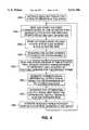
- FIG. 4is a flow diagram summarizing an exemplary image detection method for generating the differential output signal DIFF in accordance with the present invention. Steps 300-380 of FIG. 4 are recited in terms of the events during the read out periods of each active pixel sensor 35. The generation of the corresponding photogate control signal 270 and corresponding light detection period are timed so as to enable the performance of steps 300-380 as indicated in FIG. 4.
- an active pixel sensor row 25 in the array 5is first activated for read out by generating the appropriate select control signal on the corresponding select control line 186 in step 300.
- each of the sensors 35When activated for read out, each of the sensors 35 generates a voltage signal at its respective output 50 representing the voltage potential present at its diffusion node 115. Since the activated sensors 35 have not been reset, the diffusion node voltages and the corresponding output voltage signals at the sensor outputs 50 correspond to the light intensities detected by sensors 35 for the previous frame.
- step 310corresponds to the closing of the first switch 140 and the resulting charging of the first capacitor 150 by the sensor output voltage signal, as described above with respect to FIGS. 2 and 3.
- step 320the diffusion nodes 115 of the activated sensors 35 are then reset to a reset voltage as indicated in step 320. Resetting of a diffusion node 115 may be accomplished with a high voltage pulse provided to the corresponding reset transistor 120 as described above with respect to FIGS. 2 and 3.
- step 340the electrical charges collected by the photogates 100 in the activated sensor row 25 are transferred to the respective diffusion wells 110.
- transferring the collected electrical charges to the respective diffusion wells 110causes the voltage of the diffusion nodes 115 to lower from their reset voltage.
- the voltages present at the activated sensors' diffusion nodes 115 and the corresponding output voltage signals provided to the differential output circuits 18represent the detected light intensity for the present frame.
- the voltage output signals for the present frameare then read and stored by the corresponding differential output circuits 18 in step 350.
- the sensor output voltage signalsare read and stored by charging the second charge storage devices 155.
- the differential output circuits 18maintain voltage potentials for the present and previous frames' detected light intensities.
- step 360a difference is taken of the stored voltages in each output circuit 18 to yield difference output signals.
- This stepmay be accomplished using the differential amplifier 160 of FIG. 2.
- the difference output signalscorrespond to the frame-to-frame difference in the amount of detected light intensity for each of the activated pixel sensors 35.
- the difference output signalsare then sequentially provided to the imaging system output line 15, shown in FIG. 1, in a predetermined order in step 370 to form the differential output signal DIFF.
- the output signal DIFFis a serially transmitted compilation of the difference output signals for the sensors 35 of the activated row 25.
- the next sensor row 25is then activated for read out by the appropriate corresponding select control line 60 in step 380.
- Steps 310-370are then repeated for the newly activated sensor row 25 to generate the respective difference output signals to form the corresponding portion of the differential output signal DIFF.
- the image detection method of FIG. 4continuously generates difference output signals for each sensor row 25 to produce the differential output signal DIFF for consecutive detected frames during the time that the imaging system is operational.
- the differential output circuit 18may use one single-throw double-pole switch instead of the two switches 140, 145, or may consist of any configuration of components capable of providing two serially received voltage signals to a signal combiner in a parallel fashion, and generating a difference signal based on the two voltage signals.
- Other active pixel sensor implementations with different voltagesmay be readily employed.
- the array of FIG. 1has been arranged into the activation of rows and the read out of columns, the present invention may connect any number of active pixel sensors at any array position to a corresponding differential output circuit.
Landscapes
- Engineering & Computer Science (AREA)
- Multimedia (AREA)
- Signal Processing (AREA)
- Solid State Image Pick-Up Elements (AREA)
- Transforming Light Signals Into Electric Signals (AREA)
Abstract
Description
Claims (35)
Priority Applications (4)
| Application Number | Priority Date | Filing Date | Title |
|---|---|---|---|
| US08/323,203US5631704A (en) | 1994-10-14 | 1994-10-14 | Active pixel sensor and imaging system having differential mode |
| CA002156946ACA2156946A1 (en) | 1994-10-14 | 1995-08-25 | Active pixel sensor and imaging system having differential mode |
| EP95307016AEP0707416A3 (en) | 1994-10-14 | 1995-10-03 | Active pixel sensor and imaging system having differential mode |
| JP7265046AJPH08181920A (en) | 1994-10-14 | 1995-10-13 | Active picture element sensor having difference mode and imaged system |
Applications Claiming Priority (1)
| Application Number | Priority Date | Filing Date | Title |
|---|---|---|---|
| US08/323,203US5631704A (en) | 1994-10-14 | 1994-10-14 | Active pixel sensor and imaging system having differential mode |
Publications (1)
| Publication Number | Publication Date |
|---|---|
| US5631704Atrue US5631704A (en) | 1997-05-20 |
Family
ID=23258157
Family Applications (1)
| Application Number | Title | Priority Date | Filing Date |
|---|---|---|---|
| US08/323,203Expired - LifetimeUS5631704A (en) | 1994-10-14 | 1994-10-14 | Active pixel sensor and imaging system having differential mode |
Country Status (4)
| Country | Link |
|---|---|
| US (1) | US5631704A (en) |
| EP (1) | EP0707416A3 (en) |
| JP (1) | JPH08181920A (en) |
| CA (1) | CA2156946A1 (en) |
Cited By (138)
| Publication number | Priority date | Publication date | Assignee | Title |
|---|---|---|---|---|
| WO1997028558A3 (en)* | 1996-01-22 | 1997-10-02 | California Inst Of Techn | Active pixel sensor array with electronic shuttering |
| US5835141A (en)* | 1994-11-22 | 1998-11-10 | Lucent Technologies Inc. | Single-polysilicon CMOS active pixel image sensor |
| WO1998056168A1 (en)* | 1997-06-02 | 1998-12-10 | Sarnoff Corporation | Cmos image sensor with reduced fixed pattern noise |
| US5881184A (en)* | 1996-05-22 | 1999-03-09 | Eastman Kodak Company | Active pixel sensor with single pixel reset |
| US5892253A (en)* | 1997-03-26 | 1999-04-06 | Foveonics, Inc. | Active pixel sensor cell with balanced blue response and reduced noise |
| US5898196A (en)* | 1997-10-10 | 1999-04-27 | International Business Machines Corporation | Dual EPI active pixel cell design and method of making the same |
| US5900623A (en)* | 1997-08-11 | 1999-05-04 | Chrontel, Inc. | Active pixel sensor using CMOS technology with reverse biased photodiodes |
| US5909041A (en)* | 1997-11-21 | 1999-06-01 | Xerox Corporation | Photogate sensor with improved responsivity |
| US5920345A (en)* | 1997-06-02 | 1999-07-06 | Sarnoff Corporation | CMOS image sensor with improved fill factor |
| US5923369A (en)* | 1997-07-23 | 1999-07-13 | Foveonics, Inc. | Active pixel sensor cell with differential amplifier and array including same |
| US5939742A (en)* | 1997-02-10 | 1999-08-17 | Lucent Technologies Inc. | Field-effect photo-transistor |
| US5949061A (en)* | 1997-02-27 | 1999-09-07 | Eastman Kodak Company | Active pixel sensor with switched supply row select |
| US5955753A (en)* | 1995-08-02 | 1999-09-21 | Canon Kabushiki Kaisha | Solid-state image pickup apparatus and image pickup apparatus |
| WO1999057605A1 (en)* | 1998-05-05 | 1999-11-11 | Intel Corporation | Method and apparatus for processing a photocurrent in both discrete and continuous time |
| US5986297A (en)* | 1996-05-22 | 1999-11-16 | Eastman Kodak Company | Color active pixel sensor with electronic shuttering, anti-blooming and low cross-talk |
| US6008486A (en)* | 1997-12-31 | 1999-12-28 | Gentex Corporation | Wide dynamic range optical sensor |
| WO2000007360A1 (en)* | 1998-07-31 | 2000-02-10 | Intel Corporation | An improved light sensor and a method of employing the improved light sensor to capture and process image data |
| US6054704A (en)* | 1998-06-30 | 2000-04-25 | Foveon, Inc. | Driven capacitor storage pixel sensor and array |
| US6069376A (en)* | 1998-03-26 | 2000-05-30 | Foveonics, Inc. | Intra-pixel frame storage element, array, and electronic shutter method including speed switch suitable for electronic still camera applications |
| US6147846A (en)* | 1998-12-01 | 2000-11-14 | Agilent Technologies, Inc. | Drive circuit with over-voltage protection for use with pixel cells and other circuits |
| US6160281A (en)* | 1997-02-28 | 2000-12-12 | Eastman Kodak Company | Active pixel sensor with inter-pixel function sharing |
| US6160282A (en)* | 1998-04-21 | 2000-12-12 | Foveon, Inc. | CMOS image sensor employing silicide exclusion mask to reduce leakage and improve performance |
| US6166768A (en)* | 1994-01-28 | 2000-12-26 | California Institute Of Technology | Active pixel sensor array with simple floating gate pixels |
| US6201572B1 (en)* | 1998-02-02 | 2001-03-13 | Agilent Technologies, Inc. | Analog current mode assisted differential to single-ended read-out channel operable with an active pixel sensor |
| US6218692B1 (en) | 1999-11-23 | 2001-04-17 | Eastman Kodak Company | Color active pixel sensor with electronic shuttering, anti-blooming and low cross talk |
| US6218656B1 (en) | 1998-12-30 | 2001-04-17 | Eastman Kodak Company | Photodiode active pixel sensor with shared reset signal row select |
| US6233013B1 (en) | 1997-10-23 | 2001-05-15 | Xerox Corporation | Color readout system for an active pixel image sensor |
| US6246043B1 (en) | 1998-09-22 | 2001-06-12 | Foveon, Inc. | Method and apparatus for biasing a CMOS active pixel sensor above the nominal voltage maximums for an IC process |
| US6285018B1 (en) | 1999-07-20 | 2001-09-04 | Intevac, Inc. | Electron bombarded active pixel sensor |
| US6307586B1 (en) | 1999-07-20 | 2001-10-23 | Intevac, Inc. | Electron bombarded active pixel sensor camera incorporating gain control |
| US6313876B1 (en)* | 1995-06-07 | 2001-11-06 | Ivp Integrated Vision Products Ab Teknikringen | Sensor element array for reading and processing image information |
| US6323476B1 (en)* | 1996-05-22 | 2001-11-27 | Eastman Kodak Company | Active pixel sensor with switched supply row select |
| US6365886B1 (en) | 1998-02-18 | 2002-04-02 | Photobit Corporation | Smart column controls for high speed multi-resolution sensors |
| US6365926B1 (en) | 2000-09-20 | 2002-04-02 | Eastman Kodak Company | CMOS active pixel with scavenging diode |
| US6369853B1 (en) | 1997-11-13 | 2002-04-09 | Foveon, Inc. | Intra-pixel frame storage element, array, and electronic shutter method suitable for electronic still camera applications |
| US6384395B1 (en)* | 1999-06-23 | 2002-05-07 | Agence Spatiale Europeenne | Active pixel type detector |
| US6388241B1 (en) | 1998-02-19 | 2002-05-14 | Photobit Corporation | Active pixel color linear sensor with line—packed pixel readout |
| US20020060741A1 (en)* | 2000-10-27 | 2002-05-23 | Nikon Corporation | Image capturing apparatus, method for capturing image and camera |
| US6410899B1 (en) | 1998-06-17 | 2002-06-25 | Foveon, Inc. | Active pixel sensor with bootstrap amplification and reduced leakage during readout |
| US6452633B1 (en) | 1998-02-26 | 2002-09-17 | Foveon, Inc. | Exposure control in electronic cameras by detecting overflow from active pixels |
| US6452632B1 (en) | 1997-01-31 | 2002-09-17 | Kabushiki Kaisha Toshiba | Solid state image sensor and video system using the same |
| US6456326B2 (en) | 1994-01-28 | 2002-09-24 | California Institute Of Technology | Single chip camera device having double sampling operation |
| US6476864B1 (en) | 1998-05-11 | 2002-11-05 | Agilent Technologies, Inc. | Pixel sensor column amplifier architecture |
| US6486503B1 (en) | 1994-01-28 | 2002-11-26 | California Institute Of Technology | Active pixel sensor array with electronic shuttering |
| US6501506B1 (en)* | 1997-03-18 | 2002-12-31 | Kabushiki Kaisha Toshiba | Solid image pick-up unit and driving method therefor |
| US6504195B2 (en) | 2000-12-29 | 2003-01-07 | Eastman Kodak Company | Alternate method for photodiode formation in CMOS image sensors |
| US20030013328A1 (en)* | 2001-05-22 | 2003-01-16 | Andrade Thomas L. | Connection assembly for integrated circuit sensors |
| US6509832B1 (en) | 1998-09-15 | 2003-01-21 | Gentex Corporation | Systems and components for enhancing rear vision from a vehicle |
| US6512544B1 (en) | 1998-06-17 | 2003-01-28 | Foveon, Inc. | Storage pixel sensor and array with compression |
| US6512858B2 (en) | 1998-07-21 | 2003-01-28 | Foveon, Inc. | Image scanning circuitry with row and column addressing for use in electronic cameras |
| US20030020495A1 (en)* | 2001-05-22 | 2003-01-30 | Andrade Thomas L. | Surface capacitance sensor system using buried stimulus electrode |
| US6538693B1 (en)* | 1996-01-24 | 2003-03-25 | Canon Kabushiki Kaisha | Photoelectric conversion apparatus having reset noise holding and removing units |
| US6549235B1 (en) | 1994-01-28 | 2003-04-15 | California Institute Of Technology | Single substrate camera device with CMOS image sensor |
| US6563540B2 (en) | 1999-02-26 | 2003-05-13 | Intel Corporation | Light sensor with increased dynamic range |
| US20030101348A1 (en)* | 2001-07-12 | 2003-05-29 | Russo Anthony P. | Method and system for determining confidence in a digital transaction |
| US20030103141A1 (en)* | 1997-12-31 | 2003-06-05 | Bechtel Jon H. | Vehicle vision system |
| US6590611B1 (en) | 1997-11-28 | 2003-07-08 | Nikon Corporation | Solid-state image-pickup devices and methods for motion detection |
| US6597398B1 (en)* | 1999-06-02 | 2003-07-22 | Intel Corporation | Image sensor response enhancement using fluorescent phosphors |
| US20030141436A1 (en)* | 2002-01-29 | 2003-07-31 | Canon Kabushiki Kaisha | Solid image pick-up apparatus |
| US6624850B1 (en) | 1998-12-30 | 2003-09-23 | Eastman Kodak Company | Photogate active pixel sensor with high fill factor and correlated double sampling |
| US6624849B1 (en) | 1997-12-08 | 2003-09-23 | Nikon Corporation | Solid-state imaging apparatus for motion detection |
| US20030189160A1 (en)* | 2002-04-09 | 2003-10-09 | Katsuhito Sakurai | Solid-state image sensing apparatus and image sensing system |
| US6633335B1 (en) | 1998-02-28 | 2003-10-14 | Hyundai Electronics Industries Co., Ltd. | CMOS image sensor with testing circuit for verifying operation thereof |
| US6657178B2 (en) | 1999-07-20 | 2003-12-02 | Intevac, Inc. | Electron bombarded passive pixel sensor imaging |
| US6657665B1 (en) | 1998-12-31 | 2003-12-02 | Eastman Kodak Company | Active Pixel Sensor with wired floating diffusions and shared amplifier |
| US6677997B1 (en) | 1998-11-05 | 2004-01-13 | Matsushita Electric Industrial Co., Ltd. | Amplifying solid-state imaging device, and method for driving the same |
| US6697114B1 (en) | 1999-08-13 | 2004-02-24 | Foveon, Inc. | Triple slope pixel sensor and arry |
| US6731335B1 (en) | 1998-05-08 | 2004-05-04 | Hyundai Electronics Industries Co., Ltd. | CMOS image sensor having common outputting transistors and method for driving the same |
| US6753904B1 (en)* | 1997-08-12 | 2004-06-22 | Nikon Corporation | Solid-state imaging apparatus for motion detection |
| US6760070B1 (en) | 2000-02-29 | 2004-07-06 | Foveon, Inc. | High-sensitivity storage pixel sensor array having auto-exposure detection |
| US6798452B1 (en) | 1997-07-28 | 2004-09-28 | Matsushita Electric Industrial Co., Ltd. | Amplifying solid-state imaging device, method for driving the same and physical quantity distribution sensing semiconductor device |
| US6798451B1 (en)* | 1999-07-09 | 2004-09-28 | Sony Corporation | Solid-state image pickup device and method for driving the same |
| US6803958B1 (en)* | 1999-03-09 | 2004-10-12 | Micron Technology, Inc. | Apparatus and method for eliminating artifacts in active pixel sensor (APS) imagers |
| US6809768B1 (en) | 2000-02-14 | 2004-10-26 | Foveon, Inc. | Double slope pixel sensor and array |
| US20050012968A1 (en)* | 2003-07-14 | 2005-01-20 | Dialog Semiconductor | Pixel with variable resolution during exposure |
| US6847399B1 (en) | 1998-03-23 | 2005-01-25 | Micron Technology, Inc. | Increasing readout speed in CMOS APS sensors through block readout |
| US6903670B1 (en) | 2002-10-04 | 2005-06-07 | Smal Camera Technologies | Circuit and method for cancellation of column pattern noise in CMOS imagers |
| US6950131B1 (en)* | 2000-09-26 | 2005-09-27 | Valley Oak Semiconductor | Simultaneous access and reset system for an active pixel sensor |
| US7088394B2 (en) | 2001-07-09 | 2006-08-08 | Micron Technology, Inc. | Charge mode active pixel sensor read-out circuit |
| US20060176401A1 (en)* | 2002-10-24 | 2006-08-10 | Turchetta Renato Andrea D | Imaging device |
| US20060203101A1 (en)* | 2005-03-14 | 2006-09-14 | Silsby Christopher D | Motion detecting camera system |
| US20070041110A1 (en)* | 2005-08-22 | 2007-02-22 | Gentex Corporation | Vehicular rearview components and assemblies |
| US20070058062A1 (en)* | 2005-09-13 | 2007-03-15 | Sougo Ohta | Solid-state image pickup device |
| US7256589B2 (en) | 2001-04-27 | 2007-08-14 | Atrua Technologies, Inc. | Capacitive sensor system with improved capacitance measuring sensitivity |
| US20070191910A1 (en)* | 2006-02-16 | 2007-08-16 | Qiushi Ren | Visual prosthesis |
| US20080031593A1 (en)* | 2006-08-07 | 2008-02-07 | Shih-Fang Chuang | Multi-layer structure unit for recording audio/video frame data and its operation method |
| US20080062294A1 (en)* | 2006-09-07 | 2008-03-13 | Canon Kabushiki Kaisha | Signal reading apparatus and image pickup system using the signal reading apparatus |
| US20080086206A1 (en)* | 2006-05-05 | 2008-04-10 | University Of Southern California | Intraocular Camera for Retinal Prostheses |
| US20090002536A1 (en)* | 2003-04-09 | 2009-01-01 | Junichi Nakamura | Biasing scheme for large format CMOS active pixel sensors |
| US20100079643A1 (en)* | 1999-04-23 | 2010-04-01 | Anders Andersson | Active Pixel Sensor With Reduced Fixed Pattern Noise |
| US20100176275A1 (en)* | 2009-01-15 | 2010-07-15 | Raytheon Company | Multipurpose Photodetector Amplifier and Control Methods |
| US7944020B1 (en) | 2006-12-22 | 2011-05-17 | Cypress Semiconductor Corporation | Reverse MIM capacitor |
| US20110217697A1 (en)* | 2008-06-25 | 2011-09-08 | Life Technologies Corporation | Methods and apparatus for measuring analytes using large scale fet arrays |
| US20110230375A1 (en)* | 2006-12-14 | 2011-09-22 | Life Technologies Corporation | Methods and apparatus for measuring analytes using large scale fet arrays |
| USRE42918E1 (en) | 1994-01-28 | 2011-11-15 | California Institute Of Technology | Single substrate camera device with CMOS image sensor |
| WO2012039812A1 (en)* | 2010-09-24 | 2012-03-29 | Life Technologies Corporation | Matched pair transistor circuits |
| US8415716B2 (en) | 2006-12-14 | 2013-04-09 | Life Technologies Corporation | Chemically sensitive sensors with feedback circuits |
| US8421437B2 (en) | 2010-06-30 | 2013-04-16 | Life Technologies Corporation | Array column integrator |
| US8552771B1 (en) | 2012-05-29 | 2013-10-08 | Life Technologies Corporation | System for reducing noise in a chemical sensor array |
| US8564703B2 (en) | 2010-08-30 | 2013-10-22 | Arnold & Richter Cine Technik Gmbh & Co. Betriebs Kg | Image sensor with overlapping pixel readout and method |
| US8592154B2 (en) | 2009-05-29 | 2013-11-26 | Life Technologies Corporation | Methods and apparatus for high speed operation of a chemically-sensitive sensor array |
| US8747748B2 (en) | 2012-01-19 | 2014-06-10 | Life Technologies Corporation | Chemical sensor with conductive cup-shaped sensor surface |
| US8753812B2 (en) | 2004-11-12 | 2014-06-17 | The Board Of Trustees Of The Leland Stanford Junior University | Charge perturbation detection method for DNA and other molecules |
| US8776573B2 (en) | 2009-05-29 | 2014-07-15 | Life Technologies Corporation | Methods and apparatus for measuring analytes |
| US8821798B2 (en) | 2012-01-19 | 2014-09-02 | Life Technologies Corporation | Titanium nitride as sensing layer for microwell structure |
| US8841217B1 (en) | 2013-03-13 | 2014-09-23 | Life Technologies Corporation | Chemical sensor with protruded sensor surface |
| US8858782B2 (en) | 2010-06-30 | 2014-10-14 | Life Technologies Corporation | Ion-sensing charge-accumulation circuits and methods |
| US8936763B2 (en) | 2008-10-22 | 2015-01-20 | Life Technologies Corporation | Integrated sensor arrays for biological and chemical analysis |
| US8962366B2 (en) | 2013-01-28 | 2015-02-24 | Life Technologies Corporation | Self-aligned well structures for low-noise chemical sensors |
| US8963216B2 (en) | 2013-03-13 | 2015-02-24 | Life Technologies Corporation | Chemical sensor with sidewall spacer sensor surface |
| US9052497B2 (en) | 2011-03-10 | 2015-06-09 | King Abdulaziz City For Science And Technology | Computing imaging data using intensity correlation interferometry |
| US9080968B2 (en) | 2013-01-04 | 2015-07-14 | Life Technologies Corporation | Methods and systems for point of use removal of sacrificial material |
| US9099214B2 (en) | 2011-04-19 | 2015-08-04 | King Abdulaziz City For Science And Technology | Controlling microparticles through a light field having controllable intensity and periodicity of maxima thereof |
| US9109251B2 (en) | 2004-06-25 | 2015-08-18 | University Of Hawaii | Ultrasensitive biosensors |
| US9116117B2 (en) | 2013-03-15 | 2015-08-25 | Life Technologies Corporation | Chemical sensor with sidewall sensor surface |
| US9128044B2 (en) | 2013-03-15 | 2015-09-08 | Life Technologies Corporation | Chemical sensors with consistent sensor surface areas |
| DE102015003134A1 (en)* | 2014-04-01 | 2015-10-01 | Viimagic Gmbh | Global shutter pixel and correction method |
| US9404920B2 (en) | 2006-12-14 | 2016-08-02 | Life Technologies Corporation | Methods and apparatus for detecting molecular interactions using FET arrays |
| US9618475B2 (en) | 2010-09-15 | 2017-04-11 | Life Technologies Corporation | Methods and apparatus for measuring analytes |
| US9671363B2 (en) | 2013-03-15 | 2017-06-06 | Life Technologies Corporation | Chemical sensor with consistent sensor surface areas |
| US9823217B2 (en) | 2013-03-15 | 2017-11-21 | Life Technologies Corporation | Chemical device with thin conductive element |
| US9835585B2 (en) | 2013-03-15 | 2017-12-05 | Life Technologies Corporation | Chemical sensor with protruded sensor surface |
| US9841398B2 (en) | 2013-01-08 | 2017-12-12 | Life Technologies Corporation | Methods for manufacturing well structures for low-noise chemical sensors |
| TWI611695B (en)* | 2013-04-30 | 2018-01-11 | 富士軟片股份有限公司 | Solid-state photographic element and photographic device |
| TWI611696B (en)* | 2013-06-04 | 2018-01-11 | 富士軟片股份有限公司 | Solid-state imaging element and imaging device |
| US9960253B2 (en) | 2010-07-03 | 2018-05-01 | Life Technologies Corporation | Chemically sensitive sensor with lightly doped drains |
| US9972656B2 (en) | 2011-12-02 | 2018-05-15 | Arnold & Richter Cine Technik Gmbh & Co. Betriebs Kg | Image sensor and method of reading out an image sensor |
| US9970984B2 (en) | 2011-12-01 | 2018-05-15 | Life Technologies Corporation | Method and apparatus for identifying defects in a chemical sensor array |
| US10077472B2 (en) | 2014-12-18 | 2018-09-18 | Life Technologies Corporation | High data rate integrated circuit with power management |
| US10100357B2 (en) | 2013-05-09 | 2018-10-16 | Life Technologies Corporation | Windowed sequencing |
| US10379079B2 (en) | 2014-12-18 | 2019-08-13 | Life Technologies Corporation | Methods and apparatus for measuring analytes using large scale FET arrays |
| US10451585B2 (en) | 2009-05-29 | 2019-10-22 | Life Technologies Corporation | Methods and apparatus for measuring analytes |
| US10458942B2 (en) | 2013-06-10 | 2019-10-29 | Life Technologies Corporation | Chemical sensor array having multiple sensors per well |
| US10605767B2 (en) | 2014-12-18 | 2020-03-31 | Life Technologies Corporation | High data rate integrated circuit with transmitter configuration |
| US11231451B2 (en) | 2010-06-30 | 2022-01-25 | Life Technologies Corporation | Methods and apparatus for testing ISFET arrays |
| US11272132B2 (en) | 2019-06-07 | 2022-03-08 | Pacific Biosciences Of California, Inc. | Temporal differential active pixel sensor |
| US11307166B2 (en) | 2010-07-01 | 2022-04-19 | Life Technologies Corporation | Column ADC |
| US11339430B2 (en) | 2007-07-10 | 2022-05-24 | Life Technologies Corporation | Methods and apparatus for measuring analytes using large scale FET arrays |
Families Citing this family (8)
| Publication number | Priority date | Publication date | Assignee | Title |
|---|---|---|---|---|
| US5912942A (en)* | 1997-06-06 | 1999-06-15 | Schick Technologies, Inc. | X-ray detection system using active pixel sensors |
| US5898753A (en)* | 1997-06-06 | 1999-04-27 | Schick Technologies, Inc. | Apparatus for measuring bone density using active pixel sensors |
| WO2000005874A1 (en)* | 1998-07-22 | 2000-02-03 | Foveon, Inc. | Multiple storage node active pixel sensors |
| US6777663B2 (en)* | 1999-05-07 | 2004-08-17 | Intel Corporation | Enhanced Photocell with sample and hold amplifier |
| US6525304B1 (en) | 2000-11-28 | 2003-02-25 | Foveon, Inc. | Circuitry for converting analog signals from pixel sensor to a digital and for storing the digital signal |
| EP1463306B8 (en) | 2003-03-25 | 2009-11-11 | Panasonic Corporation | Imaging device that prevents loss of shadow detail |
| FR3008208B1 (en)* | 2013-07-02 | 2016-12-02 | Mbda France | METHOD AND DEVICE FOR THE DETECTION OF FIRE FROM LIGHT WEAPONS |
| US11706542B2 (en)* | 2020-09-01 | 2023-07-18 | Pixart Imaging Inc. | Pixel circuit outputting time difference data and image data, and operating method of pixel array |
Citations (3)
| Publication number | Priority date | Publication date | Assignee | Title |
|---|---|---|---|---|
| US5153420A (en)* | 1990-11-28 | 1992-10-06 | Xerox Corporation | Timing independent pixel-scale light sensing apparatus |
| US5355165A (en)* | 1992-08-06 | 1994-10-11 | Princeton Scientific Instruments, Inc. | Very high frame rate CCD imager |
| US5471515A (en)* | 1994-01-28 | 1995-11-28 | California Institute Of Technology | Active pixel sensor with intra-pixel charge transfer |
Family Cites Families (3)
| Publication number | Priority date | Publication date | Assignee | Title |
|---|---|---|---|---|
| US4219845A (en)* | 1979-04-12 | 1980-08-26 | The United States Of America As Represented By The Secretary Of The Air Force | Sense and inject moving target indicator apparatus |
| US5381013A (en)* | 1985-12-11 | 1995-01-10 | General Imaging Corporation | X-ray imaging system and solid state detector therefor |
| GB2186149B (en)* | 1985-12-23 | 1989-10-18 | Dr John Gordon Rushbrooke | Improvements in and relating to x-ray analysis systems |
- 1994
- 1994-10-14USUS08/323,203patent/US5631704A/ennot_activeExpired - Lifetime
- 1995
- 1995-08-25CACA002156946Apatent/CA2156946A1/ennot_activeAbandoned
- 1995-10-03EPEP95307016Apatent/EP0707416A3/ennot_activeWithdrawn
- 1995-10-13JPJP7265046Apatent/JPH08181920A/ennot_activeWithdrawn
Patent Citations (3)
| Publication number | Priority date | Publication date | Assignee | Title |
|---|---|---|---|---|
| US5153420A (en)* | 1990-11-28 | 1992-10-06 | Xerox Corporation | Timing independent pixel-scale light sensing apparatus |
| US5355165A (en)* | 1992-08-06 | 1994-10-11 | Princeton Scientific Instruments, Inc. | Very high frame rate CCD imager |
| US5471515A (en)* | 1994-01-28 | 1995-11-28 | California Institute Of Technology | Active pixel sensor with intra-pixel charge transfer |
Cited By (306)
| Publication number | Priority date | Publication date | Assignee | Title |
|---|---|---|---|---|
| US6456326B2 (en) | 1994-01-28 | 2002-09-24 | California Institute Of Technology | Single chip camera device having double sampling operation |
| US7105371B2 (en) | 1994-01-28 | 2006-09-12 | California Institute Of Technology | Method of acquiring an image from an optical structure having pixels with dedicated readout circuits |
| US6744068B2 (en) | 1994-01-28 | 2004-06-01 | California Institute Of Technology | Active pixel sensor with intra-pixel charge transfer |
| US6486503B1 (en) | 1994-01-28 | 2002-11-26 | California Institute Of Technology | Active pixel sensor array with electronic shuttering |
| USRE42974E1 (en) | 1994-01-28 | 2011-11-29 | California Institute Of Technology | CMOS active pixel sensor type imaging system on a chip |
| US6943838B2 (en)* | 1994-01-28 | 2005-09-13 | California Institute Of Technology | Active pixel sensor pixel having a photodetector whose output is coupled to an output transistor gate |
| US6549235B1 (en) | 1994-01-28 | 2003-04-15 | California Institute Of Technology | Single substrate camera device with CMOS image sensor |
| US7369166B2 (en) | 1994-01-28 | 2008-05-06 | California Institute Of Technology | Single substrate camera device with CMOS image sensor |
| US6555842B1 (en) | 1994-01-28 | 2003-04-29 | California Institute Of Technology | Active pixel sensor with intra-pixel charge transfer |
| US6166768A (en)* | 1994-01-28 | 2000-12-26 | California Institute Of Technology | Active pixel sensor array with simple floating gate pixels |
| USRE42918E1 (en) | 1994-01-28 | 2011-11-15 | California Institute Of Technology | Single substrate camera device with CMOS image sensor |
| US20040160522A1 (en)* | 1994-01-28 | 2004-08-19 | California Institute Of Technology | Active pixel sensor with intra-pixel charge transfer |
| US20030160238A1 (en)* | 1994-01-28 | 2003-08-28 | California Institute Of Technology, A California Corporation | Active pixel sensor with intra-pixel charge transfer |
| US5835141A (en)* | 1994-11-22 | 1998-11-10 | Lucent Technologies Inc. | Single-polysilicon CMOS active pixel image sensor |
| US6313876B1 (en)* | 1995-06-07 | 2001-11-06 | Ivp Integrated Vision Products Ab Teknikringen | Sensor element array for reading and processing image information |
| US5955753A (en)* | 1995-08-02 | 1999-09-21 | Canon Kabushiki Kaisha | Solid-state image pickup apparatus and image pickup apparatus |
| WO1997028558A3 (en)* | 1996-01-22 | 1997-10-02 | California Inst Of Techn | Active pixel sensor array with electronic shuttering |
| US6538693B1 (en)* | 1996-01-24 | 2003-03-25 | Canon Kabushiki Kaisha | Photoelectric conversion apparatus having reset noise holding and removing units |
| US6323476B1 (en)* | 1996-05-22 | 2001-11-27 | Eastman Kodak Company | Active pixel sensor with switched supply row select |
| US5986297A (en)* | 1996-05-22 | 1999-11-16 | Eastman Kodak Company | Color active pixel sensor with electronic shuttering, anti-blooming and low cross-talk |
| US5881184A (en)* | 1996-05-22 | 1999-03-09 | Eastman Kodak Company | Active pixel sensor with single pixel reset |
| US6550949B1 (en) | 1996-06-13 | 2003-04-22 | Gentex Corporation | Systems and components for enhancing rear vision from a vehicle |
| US20020145669A1 (en)* | 1997-01-31 | 2002-10-10 | Masafumi Umeda | Solid state image sensor and video system using the same |
| US6452632B1 (en) | 1997-01-31 | 2002-09-17 | Kabushiki Kaisha Toshiba | Solid state image sensor and video system using the same |
| US7012635B2 (en) | 1997-01-31 | 2006-03-14 | Kabushiki Kaisha Toshiba | Solid state image sensor and video system using the same |
| USRE44888E1 (en) | 1997-01-31 | 2014-05-13 | Kabushiki Kaisha Toshiba | Solid state image sensor and video system using the same |
| US5939742A (en)* | 1997-02-10 | 1999-08-17 | Lucent Technologies Inc. | Field-effect photo-transistor |
| US5949061A (en)* | 1997-02-27 | 1999-09-07 | Eastman Kodak Company | Active pixel sensor with switched supply row select |
| US6160281A (en)* | 1997-02-28 | 2000-12-12 | Eastman Kodak Company | Active pixel sensor with inter-pixel function sharing |
| US6423994B1 (en) | 1997-02-28 | 2002-07-23 | Eastman Kodak Company | Active pixel sensor with inter-pixel function sharing |
| US6501506B1 (en)* | 1997-03-18 | 2002-12-31 | Kabushiki Kaisha Toshiba | Solid image pick-up unit and driving method therefor |
| US5892253A (en)* | 1997-03-26 | 1999-04-06 | Foveonics, Inc. | Active pixel sensor cell with balanced blue response and reduced noise |
| WO1998056168A1 (en)* | 1997-06-02 | 1998-12-10 | Sarnoff Corporation | Cmos image sensor with reduced fixed pattern noise |
| US6320616B1 (en) | 1997-06-02 | 2001-11-20 | Sarnoff Corporation | CMOS image sensor with reduced fixed pattern noise |
| US5920345A (en)* | 1997-06-02 | 1999-07-06 | Sarnoff Corporation | CMOS image sensor with improved fill factor |
| US5923369A (en)* | 1997-07-23 | 1999-07-13 | Foveonics, Inc. | Active pixel sensor cell with differential amplifier and array including same |
| US6798452B1 (en) | 1997-07-28 | 2004-09-28 | Matsushita Electric Industrial Co., Ltd. | Amplifying solid-state imaging device, method for driving the same and physical quantity distribution sensing semiconductor device |
| US5900623A (en)* | 1997-08-11 | 1999-05-04 | Chrontel, Inc. | Active pixel sensor using CMOS technology with reverse biased photodiodes |
| US6753904B1 (en)* | 1997-08-12 | 2004-06-22 | Nikon Corporation | Solid-state imaging apparatus for motion detection |
| US6333204B1 (en) | 1997-10-10 | 2001-12-25 | International Business Machines Corporation | Dual EPI active pixel cell design and method of making the same |
| US5898196A (en)* | 1997-10-10 | 1999-04-27 | International Business Machines Corporation | Dual EPI active pixel cell design and method of making the same |
| US6233013B1 (en) | 1997-10-23 | 2001-05-15 | Xerox Corporation | Color readout system for an active pixel image sensor |
| US6369853B1 (en) | 1997-11-13 | 2002-04-09 | Foveon, Inc. | Intra-pixel frame storage element, array, and electronic shutter method suitable for electronic still camera applications |
| US5909041A (en)* | 1997-11-21 | 1999-06-01 | Xerox Corporation | Photogate sensor with improved responsivity |
| US6590611B1 (en) | 1997-11-28 | 2003-07-08 | Nikon Corporation | Solid-state image-pickup devices and methods for motion detection |
| US6624849B1 (en) | 1997-12-08 | 2003-09-23 | Nikon Corporation | Solid-state imaging apparatus for motion detection |
| US20030103141A1 (en)* | 1997-12-31 | 2003-06-05 | Bechtel Jon H. | Vehicle vision system |
| US6008486A (en)* | 1997-12-31 | 1999-12-28 | Gentex Corporation | Wide dynamic range optical sensor |
| US7567291B2 (en) | 1997-12-31 | 2009-07-28 | Gentex Corporation | Vehicle vision system |
| US6201572B1 (en)* | 1998-02-02 | 2001-03-13 | Agilent Technologies, Inc. | Analog current mode assisted differential to single-ended read-out channel operable with an active pixel sensor |
| US6365886B1 (en) | 1998-02-18 | 2002-04-02 | Photobit Corporation | Smart column controls for high speed multi-resolution sensors |
| US6388241B1 (en) | 1998-02-19 | 2002-05-14 | Photobit Corporation | Active pixel color linear sensor with line—packed pixel readout |
| US6507011B2 (en) | 1998-02-19 | 2003-01-14 | Micron Technology, Inc. | Active pixel color linear sensor with line-packed pixel readout |
| US6452633B1 (en) | 1998-02-26 | 2002-09-17 | Foveon, Inc. | Exposure control in electronic cameras by detecting overflow from active pixels |
| US6833871B1 (en) | 1998-02-26 | 2004-12-21 | Foveon, Inc. | Exposure control in electronic cameras by detecting overflow from active pixels |
| US6633335B1 (en) | 1998-02-28 | 2003-10-14 | Hyundai Electronics Industries Co., Ltd. | CMOS image sensor with testing circuit for verifying operation thereof |
| US7671914B2 (en) | 1998-03-23 | 2010-03-02 | Micron Technology Inc. | Increasing readout speed in CMOS APS sensors through block readout |
| US20050151058A1 (en)* | 1998-03-23 | 2005-07-14 | Lin-Ping Ang | Increasing readout speed in CMOS APS sensors through block readout |
| US20100103301A1 (en)* | 1998-03-23 | 2010-04-29 | Lin-Ping Ang | Increasing readout speed in cmos aps sensors through block readout |
| US6847399B1 (en) | 1998-03-23 | 2005-01-25 | Micron Technology, Inc. | Increasing readout speed in CMOS APS sensors through block readout |
| US8054362B2 (en) | 1998-03-23 | 2011-11-08 | Round Rock Research, Llc | Increasing readout speed in CMOS APS sensors through block readout |
| US20100078544A1 (en)* | 1998-03-23 | 2010-04-01 | Lin-Ping Ang | Increasing readout speed in cmos aps sensors through block readout |
| US8054361B2 (en) | 1998-03-23 | 2011-11-08 | Round Rock Research, Llc | Increasing readout speed in CMOS aps sensors through block readout |
| US8514310B2 (en) | 1998-03-23 | 2013-08-20 | Round Rock Research, Llc | Increasing readout speed in CMOS APS sensors through group readout |
| US6069376A (en)* | 1998-03-26 | 2000-05-30 | Foveonics, Inc. | Intra-pixel frame storage element, array, and electronic shutter method including speed switch suitable for electronic still camera applications |
| US6160282A (en)* | 1998-04-21 | 2000-12-12 | Foveon, Inc. | CMOS image sensor employing silicide exclusion mask to reduce leakage and improve performance |
| US6741282B1 (en) | 1998-05-05 | 2004-05-25 | Intel Corporation | Method and apparatus for processing a photocurrent in both discrete and continuous time |
| WO1999057605A1 (en)* | 1998-05-05 | 1999-11-11 | Intel Corporation | Method and apparatus for processing a photocurrent in both discrete and continuous time |
| US6731335B1 (en) | 1998-05-08 | 2004-05-04 | Hyundai Electronics Industries Co., Ltd. | CMOS image sensor having common outputting transistors and method for driving the same |
| US6476864B1 (en) | 1998-05-11 | 2002-11-05 | Agilent Technologies, Inc. | Pixel sensor column amplifier architecture |
| US6410899B1 (en) | 1998-06-17 | 2002-06-25 | Foveon, Inc. | Active pixel sensor with bootstrap amplification and reduced leakage during readout |
| US6512544B1 (en) | 1998-06-17 | 2003-01-28 | Foveon, Inc. | Storage pixel sensor and array with compression |
| US6054704A (en)* | 1998-06-30 | 2000-04-25 | Foveon, Inc. | Driven capacitor storage pixel sensor and array |
| US6636261B1 (en) | 1998-06-30 | 2003-10-21 | Foveon, Inc. | Driven capacitor storage pixel sensor and array |
| US6512858B2 (en) | 1998-07-21 | 2003-01-28 | Foveon, Inc. | Image scanning circuitry with row and column addressing for use in electronic cameras |
| GB2354664B (en)* | 1998-07-31 | 2002-10-23 | Intel Corp | An improved light sensor and a method of employing the improved light sensor to capture and process image data |
| WO2000007360A1 (en)* | 1998-07-31 | 2000-02-10 | Intel Corporation | An improved light sensor and a method of employing the improved light sensor to capture and process image data |
| GB2354664A (en)* | 1998-07-31 | 2001-03-28 | Intel Corp | An improved light sensor and a method of employing the improved light sensor to capture and process image data |
| US20070017642A1 (en)* | 1998-09-15 | 2007-01-25 | Bauer Frederick T | Systems and Components for Enhancing Rear Vision from a Vehicle |
| US6672745B1 (en) | 1998-09-15 | 2004-01-06 | Gentex Corporation | Systems and components for enhancing rear vision from a vehicle |
| US20040160786A1 (en)* | 1998-09-15 | 2004-08-19 | Bauer Frederick T. | Systems and components for enhancing rear vision from a vehicle |
| US7111968B2 (en) | 1998-09-15 | 2006-09-26 | Gentex Corporation | Systems and components for enhancing rear vision from a vehicle |
| US7568823B2 (en) | 1998-09-15 | 2009-08-04 | Gentex Corporation | Systems and components for enhancing rear vision from a vehicle |
| US6509832B1 (en) | 1998-09-15 | 2003-01-21 | Gentex Corporation | Systems and components for enhancing rear vision from a vehicle |
| US6246043B1 (en) | 1998-09-22 | 2001-06-12 | Foveon, Inc. | Method and apparatus for biasing a CMOS active pixel sensor above the nominal voltage maximums for an IC process |
| US6677997B1 (en) | 1998-11-05 | 2004-01-13 | Matsushita Electric Industrial Co., Ltd. | Amplifying solid-state imaging device, and method for driving the same |
| US6380976B1 (en)* | 1998-12-01 | 2002-04-30 | Agilent Technologies, Inc. | Drive circuit with over-voltage protection for use with pixel cells and other circuits |
| US6147846A (en)* | 1998-12-01 | 2000-11-14 | Agilent Technologies, Inc. | Drive circuit with over-voltage protection for use with pixel cells and other circuits |
| SG73652A1 (en)* | 1998-12-01 | 2001-06-19 | Agilent Technologies Inc | Drive circuit with over-voltage protection for use with pixel cells and other circuits |
| US6624850B1 (en) | 1998-12-30 | 2003-09-23 | Eastman Kodak Company | Photogate active pixel sensor with high fill factor and correlated double sampling |
| US6218656B1 (en) | 1998-12-30 | 2001-04-17 | Eastman Kodak Company | Photodiode active pixel sensor with shared reset signal row select |
| US6657665B1 (en) | 1998-12-31 | 2003-12-02 | Eastman Kodak Company | Active Pixel Sensor with wired floating diffusions and shared amplifier |
| US6563540B2 (en) | 1999-02-26 | 2003-05-13 | Intel Corporation | Light sensor with increased dynamic range |
| US8279314B2 (en) | 1999-03-09 | 2012-10-02 | Micron Technology, Inc. | Apparatus and method for eliminating artifacts in active pixel sensor (APS) imagers |
| US20090015700A1 (en)* | 1999-03-09 | 2009-01-15 | Wang Yibing Michelle | Apparatus and method for eliminating artifacts in active pixel sensor (APS) imagers |
| US6803958B1 (en)* | 1999-03-09 | 2004-10-12 | Micron Technology, Inc. | Apparatus and method for eliminating artifacts in active pixel sensor (APS) imagers |
| US20050023426A1 (en)* | 1999-03-09 | 2005-02-03 | Wang Yibing (Michelle) | Apparatus and method for eliminating artifacts in active pixel sensor (APS) imagers |
| US10063799B2 (en) | 1999-03-09 | 2018-08-28 | Micron Technology, Inc. | Apparatus and method for eliminating artifacts in active pixel sensor (APS) imagers |
| US20110102645A1 (en)* | 1999-03-09 | 2011-05-05 | Wang Yibing Michelle | Apparatus and method for eliminating artifacts in active pixel sensor (aps) imagers |
| US7411621B2 (en) | 1999-03-09 | 2008-08-12 | Micron Technology, Inc. | Apparatus and method for eliminating artifacts in active pixel sensor (APS) imagers |
| US8063965B2 (en) | 1999-03-09 | 2011-11-22 | Micron Technology, Inc. | Apparatus and method for eliminating artifacts in active pixel sensor (APS) imagers |
| US20100079643A1 (en)* | 1999-04-23 | 2010-04-01 | Anders Andersson | Active Pixel Sensor With Reduced Fixed Pattern Noise |
| US7973843B2 (en)* | 1999-04-23 | 2011-07-05 | Aptina Imaging Corporation | Active pixel sensor with reduced fixed pattern noise |
| US6597398B1 (en)* | 1999-06-02 | 2003-07-22 | Intel Corporation | Image sensor response enhancement using fluorescent phosphors |
| US6384395B1 (en)* | 1999-06-23 | 2002-05-07 | Agence Spatiale Europeenne | Active pixel type detector |
| US6798451B1 (en)* | 1999-07-09 | 2004-09-28 | Sony Corporation | Solid-state image pickup device and method for driving the same |
| US6285018B1 (en) | 1999-07-20 | 2001-09-04 | Intevac, Inc. | Electron bombarded active pixel sensor |
| US6307586B1 (en) | 1999-07-20 | 2001-10-23 | Intevac, Inc. | Electron bombarded active pixel sensor camera incorporating gain control |
| US6657178B2 (en) | 1999-07-20 | 2003-12-02 | Intevac, Inc. | Electron bombarded passive pixel sensor imaging |
| US6697114B1 (en) | 1999-08-13 | 2004-02-24 | Foveon, Inc. | Triple slope pixel sensor and arry |
| US6218692B1 (en) | 1999-11-23 | 2001-04-17 | Eastman Kodak Company | Color active pixel sensor with electronic shuttering, anti-blooming and low cross talk |
| US6809768B1 (en) | 2000-02-14 | 2004-10-26 | Foveon, Inc. | Double slope pixel sensor and array |
| US6760070B1 (en) | 2000-02-29 | 2004-07-06 | Foveon, Inc. | High-sensitivity storage pixel sensor array having auto-exposure detection |
| US6882367B1 (en) | 2000-02-29 | 2005-04-19 | Foveon, Inc. | High-sensitivity storage pixel sensor having auto-exposure detection |
| US6365926B1 (en) | 2000-09-20 | 2002-04-02 | Eastman Kodak Company | CMOS active pixel with scavenging diode |
| US6950131B1 (en)* | 2000-09-26 | 2005-09-27 | Valley Oak Semiconductor | Simultaneous access and reset system for an active pixel sensor |
| US6903764B2 (en)* | 2000-10-27 | 2005-06-07 | Nikon Corporation | Image capturing apparatus, method for capturing image and camera |
| US20020060741A1 (en)* | 2000-10-27 | 2002-05-23 | Nikon Corporation | Image capturing apparatus, method for capturing image and camera |
| US6504195B2 (en) | 2000-12-29 | 2003-01-07 | Eastman Kodak Company | Alternate method for photodiode formation in CMOS image sensors |
| US7256589B2 (en) | 2001-04-27 | 2007-08-14 | Atrua Technologies, Inc. | Capacitive sensor system with improved capacitance measuring sensitivity |
| US20030013328A1 (en)* | 2001-05-22 | 2003-01-16 | Andrade Thomas L. | Connection assembly for integrated circuit sensors |
| US7259573B2 (en) | 2001-05-22 | 2007-08-21 | Atrua Technologies, Inc. | Surface capacitance sensor system using buried stimulus electrode |
| US20030020495A1 (en)* | 2001-05-22 | 2003-01-30 | Andrade Thomas L. | Surface capacitance sensor system using buried stimulus electrode |
| US7088394B2 (en) | 2001-07-09 | 2006-08-08 | Micron Technology, Inc. | Charge mode active pixel sensor read-out circuit |
| US20060278812A1 (en)* | 2001-07-09 | 2006-12-14 | Micron Technology, Inc. | Charge mode active pixel sensor read-out circuit |
| US7649558B2 (en) | 2001-07-09 | 2010-01-19 | Aptina Imaging Corporation | Charge mode active pixel sensor read-out circuit |
| US7197168B2 (en) | 2001-07-12 | 2007-03-27 | Atrua Technologies, Inc. | Method and system for biometric image assembly from multiple partial biometric frame scans |
| US20070274575A1 (en)* | 2001-07-12 | 2007-11-29 | Russo Anthony P | Method and system for biometric image assembly from multiple partial biometric frame scans |
| US20030115490A1 (en)* | 2001-07-12 | 2003-06-19 | Russo Anthony P. | Secure network and networked devices using biometrics |
| US20030101348A1 (en)* | 2001-07-12 | 2003-05-29 | Russo Anthony P. | Method and system for determining confidence in a digital transaction |
| US7751595B2 (en) | 2001-07-12 | 2010-07-06 | Authentec, Inc. | Method and system for biometric image assembly from multiple partial biometric frame scans |
| US6847026B2 (en)* | 2002-01-29 | 2005-01-25 | Canon Kabushiki Kaisha | Solid image pick-up apparatus |
| US20030141436A1 (en)* | 2002-01-29 | 2003-07-31 | Canon Kabushiki Kaisha | Solid image pick-up apparatus |
| US20030189160A1 (en)* | 2002-04-09 | 2003-10-09 | Katsuhito Sakurai | Solid-state image sensing apparatus and image sensing system |
| US7189951B2 (en)* | 2002-04-09 | 2007-03-13 | Canon Kabushiki Kaisha | Solid-state image sensing apparatus and image sensing system |
| US6903670B1 (en) | 2002-10-04 | 2005-06-07 | Smal Camera Technologies | Circuit and method for cancellation of column pattern noise in CMOS imagers |
| US20060176401A1 (en)* | 2002-10-24 | 2006-08-10 | Turchetta Renato Andrea D | Imaging device |
| US20090002536A1 (en)* | 2003-04-09 | 2009-01-01 | Junichi Nakamura | Biasing scheme for large format CMOS active pixel sensors |
| US8988568B2 (en)* | 2003-04-09 | 2015-03-24 | Micron Technology, Inc. | Biasing scheme for large format CMOS active pixel sensors |
| US20050012968A1 (en)* | 2003-07-14 | 2005-01-20 | Dialog Semiconductor | Pixel with variable resolution during exposure |
| US9109251B2 (en) | 2004-06-25 | 2015-08-18 | University Of Hawaii | Ultrasensitive biosensors |
| US10563252B2 (en) | 2004-06-25 | 2020-02-18 | University Of Hawaii | Ultrasensitive biosensors |
| US10822641B2 (en) | 2004-11-12 | 2020-11-03 | The Board Of Trustees Of The Leland Stanford Junior University | Charge perturbation detection system for DNA and other molecules |
| US9228971B2 (en) | 2004-11-12 | 2016-01-05 | The Board Of Trustees Of The Leland Stanford Junior University | Charge perturbation detection system for DNA and other molecules |
| US8753812B2 (en) | 2004-11-12 | 2014-06-17 | The Board Of Trustees Of The Leland Stanford Junior University | Charge perturbation detection method for DNA and other molecules |
| US12139749B2 (en) | 2004-11-12 | 2024-11-12 | The Board Of Trustees Of The Leland Stanford Junior University | Charge perturbation detection system for DNA and other molecules |
| US20060203101A1 (en)* | 2005-03-14 | 2006-09-14 | Silsby Christopher D | Motion detecting camera system |
| US7643056B2 (en)* | 2005-03-14 | 2010-01-05 | Aptina Imaging Corporation | Motion detecting camera system |
| US20070041110A1 (en)* | 2005-08-22 | 2007-02-22 | Gentex Corporation | Vehicular rearview components and assemblies |
| US7488083B2 (en) | 2005-08-22 | 2009-02-10 | Gentex Corporation | Vehicular rearview components and assemblies |
| US20070058062A1 (en)* | 2005-09-13 | 2007-03-15 | Sougo Ohta | Solid-state image pickup device |
| US7595829B2 (en)* | 2005-09-13 | 2009-09-29 | Panasonic Corporation | Solid-state image pickup device |
| WO2007106145A1 (en)* | 2006-02-16 | 2007-09-20 | Qiushi Ren | Visual prosthesis |
| US20070191910A1 (en)* | 2006-02-16 | 2007-08-16 | Qiushi Ren | Visual prosthesis |
| US8197539B2 (en)* | 2006-05-05 | 2012-06-12 | University Of Southern California | Intraocular camera for retinal prostheses |
| US20080086206A1 (en)* | 2006-05-05 | 2008-04-10 | University Of Southern California | Intraocular Camera for Retinal Prostheses |
| US20080031593A1 (en)* | 2006-08-07 | 2008-02-07 | Shih-Fang Chuang | Multi-layer structure unit for recording audio/video frame data and its operation method |
| US7948541B2 (en) | 2006-09-07 | 2011-05-24 | Canon Kabushiki Kaisha | Signal reading apparatus and image pickup system using the signal reading apparatus |
| US20080062294A1 (en)* | 2006-09-07 | 2008-03-13 | Canon Kabushiki Kaisha | Signal reading apparatus and image pickup system using the signal reading apparatus |
| US8797435B2 (en) | 2006-09-07 | 2014-08-05 | Canon Kabushiki Kaisha | Signal reading apparatus and image pickup system using the signal reading apparatus |
| US20110194005A1 (en)* | 2006-09-07 | 2011-08-11 | Canon Kabushiki Kaisha | Signal reading apparatus and image pickup system using the signal reading apparatus |
| US9989489B2 (en) | 2006-12-14 | 2018-06-05 | Life Technnologies Corporation | Methods for calibrating an array of chemically-sensitive sensors |
| US8426898B2 (en) | 2006-12-14 | 2013-04-23 | Life Technologies Corporation | Methods and apparatus for measuring analytes using large scale FET arrays |
| US8441044B2 (en) | 2006-12-14 | 2013-05-14 | Life Technologies Corporation | Methods for manufacturing low noise chemically-sensitive field effect transistors |
| US8445945B2 (en) | 2006-12-14 | 2013-05-21 | Life Technologies Corporation | Low noise chemically-sensitive field effect transistors |
| US8450781B2 (en) | 2006-12-14 | 2013-05-28 | Life Technologies Corporation | Methods and apparatus for measuring analytes using large scale FET arrays |
| US8415716B2 (en) | 2006-12-14 | 2013-04-09 | Life Technologies Corporation | Chemically sensitive sensors with feedback circuits |
| US12066399B2 (en) | 2006-12-14 | 2024-08-20 | Life Technologies Corporation | Methods and apparatus for measuring analytes using large scale FET arrays |
| US8492800B2 (en) | 2006-12-14 | 2013-07-23 | Life Technologies Corporation | Chemically sensitive sensors with sample and hold capacitors |
| US8496802B2 (en) | 2006-12-14 | 2013-07-30 | Life Technologies Corporation | Methods for operating chemically-sensitive sample and hold sensors |
| US8502278B2 (en) | 2006-12-14 | 2013-08-06 | Life Technologies Corporation | Chemically-sensitive sample and hold sensors |
| US8890216B2 (en) | 2006-12-14 | 2014-11-18 | Life Technologies Corporation | Methods and apparatus for measuring analytes using large scale FET arrays |
| US8519448B2 (en) | 2006-12-14 | 2013-08-27 | Life Technologies Corporation | Chemically-sensitive array with active and reference sensors |
| US9404920B2 (en) | 2006-12-14 | 2016-08-02 | Life Technologies Corporation | Methods and apparatus for detecting molecular interactions using FET arrays |
| US8530941B2 (en) | 2006-12-14 | 2013-09-10 | Life Technologies Corporation | Methods and apparatus for measuring analytes using large scale FET arrays |
| US8535513B2 (en) | 2006-12-14 | 2013-09-17 | Life Technologies Corporation | Methods and apparatus for measuring analytes using large scale FET arrays |
| US9269708B2 (en) | 2006-12-14 | 2016-02-23 | Life Technologies Corporation | Methods and apparatus for measuring analytes using large scale FET arrays |
| US8558288B2 (en) | 2006-12-14 | 2013-10-15 | Life Technologies Corporation | Methods and apparatus for measuring analytes using large scale FET arrays |
| US9951382B2 (en) | 2006-12-14 | 2018-04-24 | Life Technologies Corporation | Methods and apparatus for measuring analytes using large scale FET arrays |
| US8575664B2 (en) | 2006-12-14 | 2013-11-05 | Life Technologies Corporation | Chemically-sensitive sensor array calibration circuitry |
| US9134269B2 (en) | 2006-12-14 | 2015-09-15 | Life Technologies Corporation | Methods and apparatus for measuring analytes using large scale FET arrays |
| US10816506B2 (en) | 2006-12-14 | 2020-10-27 | Life Technologies Corporation | Method for measuring analytes using large scale chemfet arrays |
| US11435314B2 (en) | 2006-12-14 | 2022-09-06 | Life Technologies Corporation | Chemically-sensitive sensor array device |
| US8658017B2 (en) | 2006-12-14 | 2014-02-25 | Life Technologies Corporation | Methods for operating an array of chemically-sensitive sensors |
| US11732297B2 (en)* | 2006-12-14 | 2023-08-22 | Life Technologies Corporation | Methods and apparatus for measuring analytes using large scale FET arrays |
| US8685230B2 (en) | 2006-12-14 | 2014-04-01 | Life Technologies Corporation | Methods and apparatus for high-speed operation of a chemically-sensitive sensor array |
| US8692298B2 (en) | 2006-12-14 | 2014-04-08 | Life Technologies Corporation | Chemical sensor array having multiple sensors per well |
| US12140560B2 (en) | 2006-12-14 | 2024-11-12 | Life Technologies Corporation | Methods and apparatus for measuring analytes using large scale FET arrays |
| US20110230375A1 (en)* | 2006-12-14 | 2011-09-22 | Life Technologies Corporation | Methods and apparatus for measuring analytes using large scale fet arrays |
| US10203300B2 (en) | 2006-12-14 | 2019-02-12 | Life Technologies Corporation | Methods and apparatus for measuring analytes using large scale FET arrays |
| US8742472B2 (en) | 2006-12-14 | 2014-06-03 | Life Technologies Corporation | Chemically sensitive sensors with sample and hold capacitors |
| US10415079B2 (en) | 2006-12-14 | 2019-09-17 | Life Technologies Corporation | Methods and apparatus for detecting molecular interactions using FET arrays |
| US20220340965A1 (en)* | 2006-12-14 | 2022-10-27 | Life Technologies Corporation | Methods and Apparatus for Measuring Analytes Using Large Scale FET Arrays |
| US10502708B2 (en) | 2006-12-14 | 2019-12-10 | Life Technologies Corporation | Chemically-sensitive sensor array calibration circuitry |
| US9023189B2 (en) | 2006-12-14 | 2015-05-05 | Life Technologies Corporation | High density sensor array without wells |
| US8435395B2 (en) | 2006-12-14 | 2013-05-07 | Life Technologies Corporation | Methods and apparatus for measuring analytes using large scale FET arrays |
| US10633699B2 (en) | 2006-12-14 | 2020-04-28 | Life Technologies Corporation | Methods and apparatus for measuring analytes using large scale FET arrays |
| US8764969B2 (en) | 2006-12-14 | 2014-07-01 | Life Technologies Corporation | Methods for operating chemically sensitive sensors with sample and hold capacitors |
| US8766328B2 (en) | 2006-12-14 | 2014-07-01 | Life Technologies Corporation | Chemically-sensitive sample and hold sensors |
| US8426899B2 (en) | 2006-12-14 | 2013-04-23 | Life Technologies Corporation | Methods and apparatus for measuring analytes using large scale FET arrays |
| US8607424B1 (en) | 2006-12-22 | 2013-12-17 | Cypress Semiconductor Corp. | Reverse MIM capacitor |
| US7944020B1 (en) | 2006-12-22 | 2011-05-17 | Cypress Semiconductor Corporation | Reverse MIM capacitor |
| US11339430B2 (en) | 2007-07-10 | 2022-05-24 | Life Technologies Corporation | Methods and apparatus for measuring analytes using large scale FET arrays |
| US20110217697A1 (en)* | 2008-06-25 | 2011-09-08 | Life Technologies Corporation | Methods and apparatus for measuring analytes using large scale fet arrays |
| US9194000B2 (en) | 2008-06-25 | 2015-11-24 | Life Technologies Corporation | Methods and apparatus for measuring analytes using large scale FET arrays |
| US8524057B2 (en) | 2008-06-25 | 2013-09-03 | Life Technologies Corporation | Methods and apparatus for measuring analytes using large scale FET arrays |
| US8470164B2 (en) | 2008-06-25 | 2013-06-25 | Life Technologies Corporation | Methods and apparatus for measuring analytes using large scale FET arrays |
| US8936763B2 (en) | 2008-10-22 | 2015-01-20 | Life Technologies Corporation | Integrated sensor arrays for biological and chemical analysis |
| US11448613B2 (en) | 2008-10-22 | 2022-09-20 | Life Technologies Corporation | ChemFET sensor array including overlying array of wells |
| US12146853B2 (en) | 2008-10-22 | 2024-11-19 | Life Technologies Corporation | Methods and apparatus including array of reaction chambers over array of chemFET sensors for measuring analytes |
| US9944981B2 (en) | 2008-10-22 | 2018-04-17 | Life Technologies Corporation | Methods and apparatus for measuring analytes |
| US11137369B2 (en) | 2008-10-22 | 2021-10-05 | Life Technologies Corporation | Integrated sensor arrays for biological and chemical analysis |
| US11874250B2 (en) | 2008-10-22 | 2024-01-16 | Life Technologies Corporation | Integrated sensor arrays for biological and chemical analysis |
| US9964515B2 (en) | 2008-10-22 | 2018-05-08 | Life Technologies Corporation | Integrated sensor arrays for biological and chemical analysis |
| US8258451B2 (en) | 2009-01-15 | 2012-09-04 | Raytheon Company | Image capture system including multipurpose photodetector |
| US20100176275A1 (en)* | 2009-01-15 | 2010-07-15 | Raytheon Company | Multipurpose Photodetector Amplifier and Control Methods |
| US10451585B2 (en) | 2009-05-29 | 2019-10-22 | Life Technologies Corporation | Methods and apparatus for measuring analytes |
| US8592154B2 (en) | 2009-05-29 | 2013-11-26 | Life Technologies Corporation | Methods and apparatus for high speed operation of a chemically-sensitive sensor array |
| US8742469B2 (en) | 2009-05-29 | 2014-06-03 | Life Technologies Corporation | Active chemically-sensitive sensors with correlated double sampling |
| US8766327B2 (en) | 2009-05-29 | 2014-07-01 | Life Technologies Corporation | Active chemically-sensitive sensors with in-sensor current sources |
| US8822205B2 (en) | 2009-05-29 | 2014-09-02 | Life Technologies Corporation | Active chemically-sensitive sensors with source follower amplifier |
| US11692964B2 (en) | 2009-05-29 | 2023-07-04 | Life Technologies Corporation | Methods and apparatus for measuring analytes |
| US8698212B2 (en) | 2009-05-29 | 2014-04-15 | Life Technologies Corporation | Active chemically-sensitive sensors |
| US8994076B2 (en) | 2009-05-29 | 2015-03-31 | Life Technologies Corporation | Chemically-sensitive field effect transistor based pixel array with protection diodes |
| US8748947B2 (en) | 2009-05-29 | 2014-06-10 | Life Technologies Corporation | Active chemically-sensitive sensors with reset switch |
| US8776573B2 (en) | 2009-05-29 | 2014-07-15 | Life Technologies Corporation | Methods and apparatus for measuring analytes |
| US8592153B1 (en) | 2009-05-29 | 2013-11-26 | Life Technologies Corporation | Methods for manufacturing high capacitance microwell structures of chemically-sensitive sensors |
| US11768171B2 (en) | 2009-05-29 | 2023-09-26 | Life Technologies Corporation | Methods and apparatus for measuring analytes |
| US10718733B2 (en) | 2009-05-29 | 2020-07-21 | Life Technologies Corporation | Methods and apparatus for measuring analytes |
| US12038405B2 (en) | 2009-05-29 | 2024-07-16 | Life Technologies Corporation | Methods and apparatus for measuring analytes |
| US10809226B2 (en) | 2009-05-29 | 2020-10-20 | Life Technologies Corporation | Methods and apparatus for measuring analytes |
| US8912580B2 (en) | 2009-05-29 | 2014-12-16 | Life Technologies Corporation | Active chemically-sensitive sensors with in-sensor current sources |
| US9927393B2 (en) | 2009-05-29 | 2018-03-27 | Life Technologies Corporation | Methods and apparatus for measuring analytes |
| US8741680B2 (en) | 2010-06-30 | 2014-06-03 | Life Technologies Corporation | Two-transistor pixel array |
| US9239313B2 (en) | 2010-06-30 | 2016-01-19 | Life Technologies Corporation | Ion-sensing charge-accumulation circuits and methods |
| US8983783B2 (en) | 2010-06-30 | 2015-03-17 | Life Technologies Corporation | Chemical detection device having multiple flow channels |
| US8421437B2 (en) | 2010-06-30 | 2013-04-16 | Life Technologies Corporation | Array column integrator |
| US8432150B2 (en) | 2010-06-30 | 2013-04-30 | Life Technologies Corporation | Methods for operating an array column integrator |
| US8432149B2 (en) | 2010-06-30 | 2013-04-30 | Life Technologies Corporation | Array column integrator |
| US8487790B2 (en) | 2010-06-30 | 2013-07-16 | Life Technologies Corporation | Chemical detection circuit including a serializer circuit |
| US8742471B2 (en) | 2010-06-30 | 2014-06-03 | Life Technologies Corporation | Chemical sensor array with leakage compensation circuit |
| US12038406B2 (en) | 2010-06-30 | 2024-07-16 | Life Technologies Corporation | Semiconductor-based chemical detection device |
| US10641729B2 (en) | 2010-06-30 | 2020-05-05 | Life Technologies Corporation | Column ADC |
| US8731847B2 (en) | 2010-06-30 | 2014-05-20 | Life Technologies Corporation | Array configuration and readout scheme |
| US11231451B2 (en) | 2010-06-30 | 2022-01-25 | Life Technologies Corporation | Methods and apparatus for testing ISFET arrays |
| US9164070B2 (en) | 2010-06-30 | 2015-10-20 | Life Technologies Corporation | Column adc |
| US10481123B2 (en) | 2010-06-30 | 2019-11-19 | Life Technologies Corporation | Ion-sensing charge-accumulation circuits and methods |
| US8858782B2 (en) | 2010-06-30 | 2014-10-14 | Life Technologies Corporation | Ion-sensing charge-accumulation circuits and methods |
| US11307166B2 (en) | 2010-07-01 | 2022-04-19 | Life Technologies Corporation | Column ADC |
| US9960253B2 (en) | 2010-07-03 | 2018-05-01 | Life Technologies Corporation | Chemically sensitive sensor with lightly doped drains |
| US8564703B2 (en) | 2010-08-30 | 2013-10-22 | Arnold & Richter Cine Technik Gmbh & Co. Betriebs Kg | Image sensor with overlapping pixel readout and method |
| US9958415B2 (en) | 2010-09-15 | 2018-05-01 | Life Technologies Corporation | ChemFET sensor including floating gate |
| US9958414B2 (en) | 2010-09-15 | 2018-05-01 | Life Technologies Corporation | Apparatus for measuring analytes including chemical sensor array |
| US12050195B2 (en) | 2010-09-15 | 2024-07-30 | Life Technologies Corporation | Methods and apparatus for measuring analytes using chemfet arrays |
| US9618475B2 (en) | 2010-09-15 | 2017-04-11 | Life Technologies Corporation | Methods and apparatus for measuring analytes |
| US9110015B2 (en) | 2010-09-24 | 2015-08-18 | Life Technologies Corporation | Method and system for delta double sampling |
| US8796036B2 (en) | 2010-09-24 | 2014-08-05 | Life Technologies Corporation | Method and system for delta double sampling |
| US8685324B2 (en) | 2010-09-24 | 2014-04-01 | Life Technologies Corporation | Matched pair transistor circuits |
| US8912005B1 (en) | 2010-09-24 | 2014-12-16 | Life Technologies Corporation | Method and system for delta double sampling |
| WO2012039812A1 (en)* | 2010-09-24 | 2012-03-29 | Life Technologies Corporation | Matched pair transistor circuits |
| TWI584650B (en)* | 2010-09-24 | 2017-05-21 | 生命技術公司 | Matched pair transistor circuits |
| US9052497B2 (en) | 2011-03-10 | 2015-06-09 | King Abdulaziz City For Science And Technology | Computing imaging data using intensity correlation interferometry |
| US9099214B2 (en) | 2011-04-19 | 2015-08-04 | King Abdulaziz City For Science And Technology | Controlling microparticles through a light field having controllable intensity and periodicity of maxima thereof |
| US9970984B2 (en) | 2011-12-01 | 2018-05-15 | Life Technologies Corporation | Method and apparatus for identifying defects in a chemical sensor array |
| US10365321B2 (en) | 2011-12-01 | 2019-07-30 | Life Technologies Corporation | Method and apparatus for identifying defects in a chemical sensor array |
| US10598723B2 (en) | 2011-12-01 | 2020-03-24 | Life Technologies Corporation | Method and apparatus for identifying defects in a chemical sensor array |
| US9972656B2 (en) | 2011-12-02 | 2018-05-15 | Arnold & Richter Cine Technik Gmbh & Co. Betriebs Kg | Image sensor and method of reading out an image sensor |
| US8747748B2 (en) | 2012-01-19 | 2014-06-10 | Life Technologies Corporation | Chemical sensor with conductive cup-shaped sensor surface |
| US8821798B2 (en) | 2012-01-19 | 2014-09-02 | Life Technologies Corporation | Titanium nitride as sensing layer for microwell structure |
| US10404249B2 (en) | 2012-05-29 | 2019-09-03 | Life Technologies Corporation | System for reducing noise in a chemical sensor array |
| US9985624B2 (en) | 2012-05-29 | 2018-05-29 | Life Technologies Corporation | System for reducing noise in a chemical sensor array |
| US8786331B2 (en) | 2012-05-29 | 2014-07-22 | Life Technologies Corporation | System for reducing noise in a chemical sensor array |
| US9270264B2 (en) | 2012-05-29 | 2016-02-23 | Life Technologies Corporation | System for reducing noise in a chemical sensor array |
| US8552771B1 (en) | 2012-05-29 | 2013-10-08 | Life Technologies Corporation | System for reducing noise in a chemical sensor array |
| US9852919B2 (en) | 2013-01-04 | 2017-12-26 | Life Technologies Corporation | Methods and systems for point of use removal of sacrificial material |
| US9080968B2 (en) | 2013-01-04 | 2015-07-14 | Life Technologies Corporation | Methods and systems for point of use removal of sacrificial material |
| US10436742B2 (en) | 2013-01-08 | 2019-10-08 | Life Technologies Corporation | Methods for manufacturing well structures for low-noise chemical sensors |
| US9841398B2 (en) | 2013-01-08 | 2017-12-12 | Life Technologies Corporation | Methods for manufacturing well structures for low-noise chemical sensors |
| US8962366B2 (en) | 2013-01-28 | 2015-02-24 | Life Technologies Corporation | Self-aligned well structures for low-noise chemical sensors |
| US9995708B2 (en) | 2013-03-13 | 2018-06-12 | Life Technologies Corporation | Chemical sensor with sidewall spacer sensor surface |
| US8963216B2 (en) | 2013-03-13 | 2015-02-24 | Life Technologies Corporation | Chemical sensor with sidewall spacer sensor surface |
| US8841217B1 (en) | 2013-03-13 | 2014-09-23 | Life Technologies Corporation | Chemical sensor with protruded sensor surface |
| US9835585B2 (en) | 2013-03-15 | 2017-12-05 | Life Technologies Corporation | Chemical sensor with protruded sensor surface |
| US9823217B2 (en) | 2013-03-15 | 2017-11-21 | Life Technologies Corporation | Chemical device with thin conductive element |
| US9128044B2 (en) | 2013-03-15 | 2015-09-08 | Life Technologies Corporation | Chemical sensors with consistent sensor surface areas |
| US10481124B2 (en) | 2013-03-15 | 2019-11-19 | Life Technologies Corporation | Chemical device with thin conductive element |
| US9116117B2 (en) | 2013-03-15 | 2015-08-25 | Life Technologies Corporation | Chemical sensor with sidewall sensor surface |
| US10422767B2 (en) | 2013-03-15 | 2019-09-24 | Life Technologies Corporation | Chemical sensor with consistent sensor surface areas |
| US9671363B2 (en) | 2013-03-15 | 2017-06-06 | Life Technologies Corporation | Chemical sensor with consistent sensor surface areas |
| TWI611695B (en)* | 2013-04-30 | 2018-01-11 | 富士軟片股份有限公司 | Solid-state photographic element and photographic device |
| US10655175B2 (en) | 2013-05-09 | 2020-05-19 | Life Technologies Corporation | Windowed sequencing |
| US10100357B2 (en) | 2013-05-09 | 2018-10-16 | Life Technologies Corporation | Windowed sequencing |
| US11028438B2 (en) | 2013-05-09 | 2021-06-08 | Life Technologies Corporation | Windowed sequencing |
| TWI611696B (en)* | 2013-06-04 | 2018-01-11 | 富士軟片股份有限公司 | Solid-state imaging element and imaging device |
| US11499938B2 (en) | 2013-06-10 | 2022-11-15 | Life Technologies Corporation | Chemical sensor array having multiple sensors per well |
| US10816504B2 (en) | 2013-06-10 | 2020-10-27 | Life Technologies Corporation | Chemical sensor array having multiple sensors per well |
| US11774401B2 (en) | 2013-06-10 | 2023-10-03 | Life Technologies Corporation | Chemical sensor array having multiple sensors per well |
| US10458942B2 (en) | 2013-06-10 | 2019-10-29 | Life Technologies Corporation | Chemical sensor array having multiple sensors per well |
| DE102015003134A1 (en)* | 2014-04-01 | 2015-10-01 | Viimagic Gmbh | Global shutter pixel and correction method |
| US10767224B2 (en) | 2014-12-18 | 2020-09-08 | Life Technologies Corporation | High data rate integrated circuit with power management |
| US11536688B2 (en) | 2014-12-18 | 2022-12-27 | Life Technologies Corporation | High data rate integrated circuit with transmitter configuration |
| US10077472B2 (en) | 2014-12-18 | 2018-09-18 | Life Technologies Corporation | High data rate integrated circuit with power management |
| US10379079B2 (en) | 2014-12-18 | 2019-08-13 | Life Technologies Corporation | Methods and apparatus for measuring analytes using large scale FET arrays |
| US10605767B2 (en) | 2014-12-18 | 2020-03-31 | Life Technologies Corporation | High data rate integrated circuit with transmitter configuration |
| US12196704B2 (en) | 2014-12-18 | 2025-01-14 | Life Technologies Corporation | High data rate integrated circuit with transmitter configuration |
| US11272132B2 (en) | 2019-06-07 | 2022-03-08 | Pacific Biosciences Of California, Inc. | Temporal differential active pixel sensor |
Also Published As
| Publication number | Publication date |
|---|---|
| EP0707416A3 (en) | 1996-09-04 |
| CA2156946A1 (en) | 1996-04-15 |
| EP0707416A2 (en) | 1996-04-17 |
| JPH08181920A (en) | 1996-07-12 |
Similar Documents
| Publication | Publication Date | Title |
|---|---|---|
| US5631704A (en) | Active pixel sensor and imaging system having differential mode | |
| US5602585A (en) | Method and system for camera with motion detection | |
| US5898168A (en) | Image sensor pixel circuit | |
| US6839452B1 (en) | Dynamically re-configurable CMOS imagers for an active vision system | |
| KR100750778B1 (en) | Photodiode active pixel sensor with shared reset signal row select | |
| JP3521109B2 (en) | Solid-state imaging device for motion detection | |
| KR100552946B1 (en) | Extended dynamic range image sensor system | |
| KR101424033B1 (en) | Solid-state imaging device, method for driving solid-state imaging device, and imaging device | |
| US8194163B2 (en) | Solid-state pickup apparatus, its driving method and camera system | |
| EP0879530B1 (en) | Current-mediated active-pixel image sensing device with current reset | |
| US7375748B2 (en) | Differential readout from pixels in CMOS sensor | |
| US8054361B2 (en) | Increasing readout speed in CMOS aps sensors through block readout | |
| EP0403248B1 (en) | Photoelectric converting apparatus | |
| US7106915B2 (en) | Methods and devices for reading out an image sensor with reduced delay time between lines | |
| JP2641802B2 (en) | Imaging device | |
| JPH04262679A (en) | Driving method for solid-state image pickup device | |
| US4626916A (en) | Solid state image pickup device | |
| US4937674A (en) | Solid-state imaging device with static induction transistor matrix | |
| US6697108B1 (en) | Fast frame readout architecture for array sensors with integrated correlated double sampling system | |
| KR100595801B1 (en) | Solid state imaging device, driving method thereof, and camera | |
| EP0869665B1 (en) | Solid state image sensor | |
| JPH02101878A (en) | solid-state imaging device | |
| WO2001038825A1 (en) | Dynamically re-configurable cmos imagers for an active vision system | |
| EP0928102B1 (en) | Array sensors | |
| JP4404261B2 (en) | Solid-state imaging device and imaging apparatus |
Legal Events
| Date | Code | Title | Description |
|---|---|---|---|
| AS | Assignment | Owner name:AT&T CORP., NEW YORK Free format text:ASSIGNMENT OF ASSIGNORS INTEREST;ASSIGNORS:DICKINSON, ALEXANDER GEORGE;EID, EL-SAYED IBRARHIM;INGLIS, DAVID ANDREW;REEL/FRAME:007307/0689 Effective date:19941107 | |
| AS | Assignment | Owner name:LUCENT TECHNOLOGIES INC., NEW JERSEY Free format text:ASSIGNMENT OF ASSIGNORS INTEREST;ASSIGNOR:AT&T CORP.;REEL/FRAME:008502/0735 Effective date:19960329 | |
| STCF | Information on status: patent grant | Free format text:PATENTED CASE | |
| FEPP | Fee payment procedure | Free format text:PAYOR NUMBER ASSIGNED (ORIGINAL EVENT CODE: ASPN); ENTITY STATUS OF PATENT OWNER: LARGE ENTITY | |
| FPAY | Fee payment | Year of fee payment:4 | |
| FEPP | Fee payment procedure | Free format text:PAYER NUMBER DE-ASSIGNED (ORIGINAL EVENT CODE: RMPN); ENTITY STATUS OF PATENT OWNER: LARGE ENTITY Free format text:PAYOR NUMBER ASSIGNED (ORIGINAL EVENT CODE: ASPN); ENTITY STATUS OF PATENT OWNER: LARGE ENTITY | |
| FPAY | Fee payment | Year of fee payment:8 | |
| FPAY | Fee payment | Year of fee payment:12 | |
| CC | Certificate of correction | ||
| AS | Assignment | Owner name:DEUTSCHE BANK AG NEW YORK BRANCH, AS COLLATERAL AG Free format text:PATENT SECURITY AGREEMENT;ASSIGNORS:LSI CORPORATION;AGERE SYSTEMS LLC;REEL/FRAME:032856/0031 Effective date:20140506 | |
| AS | Assignment | Owner name:AVAGO TECHNOLOGIES GENERAL IP (SINGAPORE) PTE. LTD Free format text:ASSIGNMENT OF ASSIGNORS INTEREST;ASSIGNOR:AGERE SYSTEMS LLC;REEL/FRAME:035365/0634 Effective date:20140804 | |
| AS | Assignment | Owner name:LSI CORPORATION, CALIFORNIA Free format text:TERMINATION AND RELEASE OF SECURITY INTEREST IN PATENT RIGHTS (RELEASES RF 032856-0031);ASSIGNOR:DEUTSCHE BANK AG NEW YORK BRANCH, AS COLLATERAL AGENT;REEL/FRAME:037684/0039 Effective date:20160201 Owner name:AGERE SYSTEMS LLC, PENNSYLVANIA Free format text:TERMINATION AND RELEASE OF SECURITY INTEREST IN PATENT RIGHTS (RELEASES RF 032856-0031);ASSIGNOR:DEUTSCHE BANK AG NEW YORK BRANCH, AS COLLATERAL AGENT;REEL/FRAME:037684/0039 Effective date:20160201 |