US5631192A - Semiconductor device on an opposed leadframe and method for making - Google Patents
Semiconductor device on an opposed leadframe and method for makingDownload PDFInfo
- Publication number
- US5631192A US5631192AUS08/537,584US53758495AUS5631192AUS 5631192 AUS5631192 AUS 5631192AUS 53758495 AUS53758495 AUS 53758495AUS 5631192 AUS5631192 AUS 5631192A
- Authority
- US
- United States
- Prior art keywords
- forming
- leadframe
- electronic component
- semiconductor device
- bonding region
- Prior art date
- Legal status (The legal status is an assumption and is not a legal conclusion. Google has not performed a legal analysis and makes no representation as to the accuracy of the status listed.)
- Expired - Lifetime
Links
Images


Classifications
- H—ELECTRICITY
- H10—SEMICONDUCTOR DEVICES; ELECTRIC SOLID-STATE DEVICES NOT OTHERWISE PROVIDED FOR
- H10F—INORGANIC SEMICONDUCTOR DEVICES SENSITIVE TO INFRARED RADIATION, LIGHT, ELECTROMAGNETIC RADIATION OF SHORTER WAVELENGTH OR CORPUSCULAR RADIATION
- H10F55/00—Radiation-sensitive semiconductor devices covered by groups H10F10/00, H10F19/00 or H10F30/00 being structurally associated with electric light sources and electrically or optically coupled thereto
- H10F55/20—Radiation-sensitive semiconductor devices covered by groups H10F10/00, H10F19/00 or H10F30/00 being structurally associated with electric light sources and electrically or optically coupled thereto wherein the electric light source controls the radiation-sensitive semiconductor devices, e.g. optocouplers
- H10F55/25—Radiation-sensitive semiconductor devices covered by groups H10F10/00, H10F19/00 or H10F30/00 being structurally associated with electric light sources and electrically or optically coupled thereto wherein the electric light source controls the radiation-sensitive semiconductor devices, e.g. optocouplers wherein the radiation-sensitive devices and the electric light source are all semiconductor devices
Definitions
- the present inventionrelates, in general, to semiconductor devices, and more particularly, to semiconductor devices formed on an opposed leadframe.
- Optoisolatorsare electronic components which transmit electrical information between a light source (emitter) and a light detector (receiver), without electrical connection.
- the light emittedcan be either invisible such as infrared or can be emitted in the visible spectrum.
- An enabling input signal to the optoisolatorcauses the light source to turn on.
- the light detectorthen senses the light from the emitter source and produces a corresponding output signal.
- the output signalis coupled to the input signal optically rather than with an electrical connection. Consequently such devices are called optoisolators.
- a high voltage circuit and a low voltage circuitmust interact in order to process data. To electrically isolate the two circuits from noise or cross talk, optoisolators are used.
- the light source and light detectorIn order for an optoisolator to operate properly, the light source and light detector must be oriented properly with respect to each other. If too little light from the emitter reaches the detector, then the sensitivity of the detector suffers. If too much light reaches the detector, then the speed performance suffers because saturation of the phototransistor on the detector will reduce the switching speed of the detector. If the spacing between the emitter and the detector is too great, light transfer efficiency will be decreased and if the distance is too short, the isolation voltage of the optoisolator is degraded.
- FIGS. 1-2are enlarged isometric views of a semiconductor device at various stages of fabrication
- FIGS. 3-5are enlarged top views of a semiconductor device at various stages of fabrication and
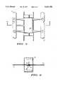
- FIG. 6is an enlarged cross-sectional view of a completed semiconductor device along the lines 6--6 of FIG. 5.
- FIG. 1is an enlarged isometric view of a semiconductor device 10 in an early stage of fabrication.
- semiconductor device 10is described as an optocoupler or an optoisolator which has two electronic components 22 and 24 formed on an opposed leadframe 11.
- the first electronic component 22is a light emitting diode referred to as an emitter and the second electronic component 24 is a light detector or receiver.
- itis necessary to electrically isolate portions of a circuit from each other, but still allow input and output signals to be communicated between the two circuits. This is necessary to prevent cross talk, noise, or high current levels from damaging the circuits. This can be prevented by optically coupling the circuits together.
- optoisolator 10uses first electronic component 22 to enable second electronic component 24 by generating a light signal.
- Light generated by emitter 22passes through a transparent medium which is in turn detected by receiver 24.
- the present inventioncan also be used to form a semiconductor device having two electronic components which may be magnetically coupled together rather than optically. In an effort to reduce the size and the number of components in an electrical circuit, it is also possible to form a semiconductor device where the two electronic devices are not coupled together, but rather simply reside in close proximity to each other.
- Optoisolator 10is formed from a single leadframe 11 having holes 26 which are used by tooling equipment to maneuver and align leadframe 11 through various assembly operations.
- Leadframe 11also has dambars 12 and interconnect bars 13 which are used to provide structural support and form optoisolator 10 during the assembly process.
- Leadframe 11can be divided into two bonding regions 30 and 31, one each for the mounting of electronic components 22 and 24 respectively.
- the first bonding region 30has a die flag 14 and a bonding lead 17 both of which are electrically connected to a lead 19.
- the second bonding region 31has a die flag 16 with bonding leads 18 which are electrically connected to by leads 20.
- leadframe 11is patterned by either a stamping or an etch process using a starting material made from copper, copper alloy, or the like. If desired, die flags 14 and 16 and bonding leads 17 and 20 can be electroplated by masking off portions of leadframe 11 and then covering the desired area with a material such as gold, nickel, or copper. The first and second bonding regions 30 and 31 are then bent to be offset or opposed relative to each other. In a forming operation, die flag 14 and bonding lead 17 is bent downward relative to the plane formed by leadframe 11 and die flag 16 and bonding leads 20 are bent up. It is not necessary that both bonding regions 30 and 31 be offset from the plane of the leadframe, in fact it is possible to bend only one of the bonding regions 30 and 31 such that one is higher than the other.
- electronic component 22is aligned and bonded to die flag 14 with either a solder pre-form, eutectic bond, or any adhesive and conductive material.
- a bonding wire 23is then formed from electronic component 22 to bonding lead 17.
- Leadframe 11is then flipped so that electronic component 24 can be bonded to die flag 16 again with either a solder pre-form, eutectic bond, or any adhesive and conductive material. If electronic component 24 is a light detector, a collector terminal is bonded to die flag 16 and then bonding wires 25 are formed between a base and an emitter terminal of electronic component 24 and bonding leads 18.
- FIG. 1is labeled with edges 35 and 36.
- FIG. 2is an enlarged isometric view of semiconductor device 10 after further processing.
- electronic component 24is brought over electronic component 22 by bending, crimping, or coining interconnect bars 13.
- bending interconnect bars 13 downward as shown by arrows 32 or upwardwill cause first and second bonding regions 30 and 31, and all of their elements, to move or slide towards each other in the direction indicated by arrows 34.
- the position of edges 35 and 36 of leadframe 11 prior to the bending operationis labeled as 35' and 36'.
- first and second bonding regions 30 and 31have been previously offset relative to each other, it is possible to form leadframe 11 such that electronic component 24 of second bonding region 31 is positioned directly over electronic component 22 of first bonding region 30 as shown in FIG. 3.
- the space between electronic components 22 and 24is determined by the thickness of each component and the amount of offset between first bonding region 30 and second bonding region 31.
- interconnect bars 13can be left on leadframe 11 to maintain the placement of electronic components 22 and 24.
- FIG. 4is an enlarged top view of semiconductor device 10 after further processing.
- An optically transparent mold compound 28is formed on leadframe 11 to encapsulate electronic components 22 and 24.
- Transparent mold 28can be formed from any material that is transparent to the frequency of light that is generated by emitter 22 such as thermal set epoxy. Since light emitter 22 is formed directly over light detector 24, the need to form a reflective coating or dome over transparent mold 28 is obviated.
- a body 29is formed around transparent mold 28 and a portion of leads 19 and 20 as shown in FIG. 5. Body 29 can be formed from any mold compound used in the industry and is formed to provide semiconductor device 10 with environmental and electrical protection.
- FIG. 6is an enlarged cross-sectional view of completed semiconductor device 10 on leadframe 11. Note final placement of electronic components 22 and 24 are opposed to each other and are offset from the plane formed by leadframe 11. It will be understood that it is possible to form semiconductor device 10 such that either of the two electronic components 22 and 24 can be in a plane formed by leadframe 11. It will also be understood that if electronic components 22 and 24 are either magnetically coupled together or not coupled at all, it may not be necessary to align electronic components 22 and 24 directly over each other and it is not necessary to form transparent mold 28.
- semiconductor device 10is trimmed and formed from leadframe 11 by removing dambars 12 releasing leads 19 and 20 from leadframe 11. To simplify the trim and form operation, it may be necessary to remove interconnect bars 13. In the present invention the sequence of mounting electronic components 22 and 24 could be reversed. It is also possible to form a semiconductor device from two electronic components that have additional bonding leads which will require additional bonding wires.
- the present inventionprovides a method for forming a semiconductor device 10, such as a optoisolator, on an opposed leadframe 11.
- a semiconductor device 10such as a optoisolator
- the forming of interconnect bars 13 to align electronic components 22 and 24 relative to each otheris a repeatable process which can be accurately controlled and adjusted.
- the presence of interconnect bars 13also improves the manufacturability of semiconductor device 10 by providing structural support to leadframe 11 during the molding operation. Since the present invention can be formed from a single stamped leadframe, the total material cost is reduced over some previously known methods that require two leadframes or the formation of a reflective coating or dome.
Landscapes
- Lead Frames For Integrated Circuits (AREA)
Abstract
Description
Claims (25)
Priority Applications (1)
| Application Number | Priority Date | Filing Date | Title |
|---|---|---|---|
| US08/537,584US5631192A (en) | 1995-10-02 | 1995-10-02 | Semiconductor device on an opposed leadframe and method for making |
Applications Claiming Priority (1)
| Application Number | Priority Date | Filing Date | Title |
|---|---|---|---|
| US08/537,584US5631192A (en) | 1995-10-02 | 1995-10-02 | Semiconductor device on an opposed leadframe and method for making |
Publications (1)
| Publication Number | Publication Date |
|---|---|
| US5631192Atrue US5631192A (en) | 1997-05-20 |
Family
ID=24143254
Family Applications (1)
| Application Number | Title | Priority Date | Filing Date |
|---|---|---|---|
| US08/537,584Expired - LifetimeUS5631192A (en) | 1995-10-02 | 1995-10-02 | Semiconductor device on an opposed leadframe and method for making |
Country Status (1)
| Country | Link |
|---|---|
| US (1) | US5631192A (en) |
Cited By (7)
| Publication number | Priority date | Publication date | Assignee | Title |
|---|---|---|---|---|
| US6246123B1 (en) | 1998-05-04 | 2001-06-12 | Motorola, Inc. | Transparent compound and applications for its use |
| US20050023441A1 (en)* | 2003-07-11 | 2005-02-03 | Kabushiki Kaisha Toshiba | Optical semiconductor device and method of manufacturing the same |
| US20080106877A1 (en)* | 2006-11-06 | 2008-05-08 | Pai Deepak K | System and method for manufacturing C-shaped leads |
| US20090152002A1 (en)* | 2007-12-13 | 2009-06-18 | Cheng-Hong Su | Optoisolator leadframe assembly |
| US20100075529A1 (en)* | 2007-03-01 | 2010-03-25 | Molex Incorporated | Terminal assembly and flat cable connector |
| JP2016207543A (en)* | 2015-04-24 | 2016-12-08 | 株式会社東芝 | Optical coupling device |
| CN109983591A (en)* | 2016-11-11 | 2019-07-05 | 亮锐控股有限公司 | The method for manufacturing lead frame |
Citations (10)
| Publication number | Priority date | Publication date | Assignee | Title |
|---|---|---|---|---|
| US3839782A (en)* | 1972-03-15 | 1974-10-08 | M Lincoln | Method for using a lead frame for the manufacture of electric devices having semiconductor chips placed in a face-to-face relation |
| US3893158A (en)* | 1972-03-15 | 1975-07-01 | Motorola Inc | Lead frame for the manufacture of electric devices having semiconductor chips placed in a face to face relation |
| US4047045A (en)* | 1975-03-03 | 1977-09-06 | Paxton Jr Grady W | Optical coupler |
| US4160308A (en)* | 1976-02-02 | 1979-07-10 | Fairchild Camera And Instrument Corporation | Optically coupled isolator device and method of making same |
| US4446375A (en)* | 1981-10-14 | 1984-05-01 | General Electric Company | Optocoupler having folded lead frame construction |
| US4633582A (en)* | 1985-08-14 | 1987-01-06 | General Instrument Corporation | Method for assembling an optoisolator and leadframe therefor |
| US5049527A (en)* | 1985-06-25 | 1991-09-17 | Hewlett-Packard Company | Optical isolator |
| US5198391A (en)* | 1991-06-15 | 1993-03-30 | Deutsche Aerospace Ag | Method for bonding llccc-components using a leadframe |
| US5389578A (en)* | 1994-01-04 | 1995-02-14 | Texas Instruments Incorporated | Optical coupler |
| US5491111A (en)* | 1994-10-26 | 1996-02-13 | Tai; George | Method of making a semiconductor diode |
- 1995
- 1995-10-02USUS08/537,584patent/US5631192A/ennot_activeExpired - Lifetime
Patent Citations (10)
| Publication number | Priority date | Publication date | Assignee | Title |
|---|---|---|---|---|
| US3839782A (en)* | 1972-03-15 | 1974-10-08 | M Lincoln | Method for using a lead frame for the manufacture of electric devices having semiconductor chips placed in a face-to-face relation |
| US3893158A (en)* | 1972-03-15 | 1975-07-01 | Motorola Inc | Lead frame for the manufacture of electric devices having semiconductor chips placed in a face to face relation |
| US4047045A (en)* | 1975-03-03 | 1977-09-06 | Paxton Jr Grady W | Optical coupler |
| US4160308A (en)* | 1976-02-02 | 1979-07-10 | Fairchild Camera And Instrument Corporation | Optically coupled isolator device and method of making same |
| US4446375A (en)* | 1981-10-14 | 1984-05-01 | General Electric Company | Optocoupler having folded lead frame construction |
| US5049527A (en)* | 1985-06-25 | 1991-09-17 | Hewlett-Packard Company | Optical isolator |
| US4633582A (en)* | 1985-08-14 | 1987-01-06 | General Instrument Corporation | Method for assembling an optoisolator and leadframe therefor |
| US5198391A (en)* | 1991-06-15 | 1993-03-30 | Deutsche Aerospace Ag | Method for bonding llccc-components using a leadframe |
| US5389578A (en)* | 1994-01-04 | 1995-02-14 | Texas Instruments Incorporated | Optical coupler |
| US5491111A (en)* | 1994-10-26 | 1996-02-13 | Tai; George | Method of making a semiconductor diode |
Cited By (15)
| Publication number | Priority date | Publication date | Assignee | Title |
|---|---|---|---|---|
| US6246123B1 (en) | 1998-05-04 | 2001-06-12 | Motorola, Inc. | Transparent compound and applications for its use |
| US20050023441A1 (en)* | 2003-07-11 | 2005-02-03 | Kabushiki Kaisha Toshiba | Optical semiconductor device and method of manufacturing the same |
| US7230259B2 (en) | 2003-07-11 | 2007-06-12 | Kabushiki Kaisha Toshiba | Optical coupling device including lead frame having a convexity and method of manufacturing the device |
| US20080106877A1 (en)* | 2006-11-06 | 2008-05-08 | Pai Deepak K | System and method for manufacturing C-shaped leads |
| US8196291B2 (en)* | 2006-11-06 | 2012-06-12 | General Dynamics Advanced Information Systems, Inc. | Method for manufacturing leads |
| US8142233B2 (en)* | 2007-03-01 | 2012-03-27 | Molex Incorporated | Terminal assembly and flat cable connector |
| US20100075529A1 (en)* | 2007-03-01 | 2010-03-25 | Molex Incorporated | Terminal assembly and flat cable connector |
| US20090152002A1 (en)* | 2007-12-13 | 2009-06-18 | Cheng-Hong Su | Optoisolator leadframe assembly |
| US8390102B2 (en)* | 2007-12-13 | 2013-03-05 | Silitek Electronic (Guangzhou) Co., Ltd. | Optoisolator leadframe assembly |
| US20130175679A1 (en)* | 2007-12-13 | 2013-07-11 | Cheng-Hong Su | Optoisolator leadframe assembly |
| US8853837B2 (en)* | 2007-12-13 | 2014-10-07 | Lite-On Electronics (Guangzhou) Limited | Optoisolator leadframe assembly |
| JP2016207543A (en)* | 2015-04-24 | 2016-12-08 | 株式会社東芝 | Optical coupling device |
| CN109983591A (en)* | 2016-11-11 | 2019-07-05 | 亮锐控股有限公司 | The method for manufacturing lead frame |
| US20190371989A1 (en)* | 2016-11-11 | 2019-12-05 | Lumileds Llc | Method of manufacturing a lead frame |
| CN109983591B (en)* | 2016-11-11 | 2022-10-04 | 亮锐控股有限公司 | Method for manufacturing lead frame |
Similar Documents
| Publication | Publication Date | Title |
|---|---|---|
| CA1272306A (en) | Support assembly for integrated circuits | |
| US5438021A (en) | Method of manufacturing a multiple-chip semiconductor device with different leadframes | |
| US5218229A (en) | Inset die lead frame configuration lead frame for a semiconductor device having means for improved busing and die-lead frame attachment | |
| EP0295459A2 (en) | Electronic assembly and method of making it | |
| US7307285B2 (en) | Optical semiconductor device and a method for manufacturing the same | |
| KR100442847B1 (en) | Power semiconductor module that has three dimensional structure and a method of manufacturing thereof | |
| KR20020009449A (en) | Semiconductor device | |
| EP0472755B1 (en) | Lead frame for an optical module | |
| JPH06112354A (en) | Thin overmolded semiconductor device and its manufacture | |
| US5631192A (en) | Semiconductor device on an opposed leadframe and method for making | |
| JPH09252014A (en) | Method for manufacturing semiconductor device | |
| JP2966591B2 (en) | Optical semiconductor device | |
| US5874354A (en) | Method for electrically connecting a semiconductor chip to at least one contact surface and smart card module and smart card produced by the method | |
| US4893169A (en) | Lead frame and a process for the production of a lead with this lead frame | |
| US5393705A (en) | Molded semiconductor device using intermediate lead pattern on film carrier formed from lattice pattern commonly available for devices and process of fabrication thereof | |
| KR970000219B1 (en) | Semiconductor device and manufacturing method thereof | |
| US5361970A (en) | Method of producing a semiconductor integrated circuit device having terminal members provided between semiconductor element and leads | |
| US11694945B2 (en) | Lead frame package having conductive surfaces | |
| US3553828A (en) | Lead assembly structure for semiconductor devices | |
| US20030082855A1 (en) | Board frame, method for fabricating thereof and method for fabricating semiconductor apparatus | |
| JP3415369B2 (en) | Optically coupled relay device | |
| US20040004277A1 (en) | Semiconductor package with reinforced substrate and fabrication method of the substrate | |
| KR0143074B1 (en) | Optical module and optical module lead frame | |
| KR970024055A (en) | High density package using simultaneously cut semiconductor chip and manufacturing method thereof | |
| JPH0529539A (en) | Multi-chip module |
Legal Events
| Date | Code | Title | Description |
|---|---|---|---|
| AS | Assignment | Owner name:MOTOROLA, INC., ILLINOIS Free format text:ASSIGNMENT OF ASSIGNORS INTEREST;ASSIGNORS:HEPPLER, RICHARD E.;SULLIVAN, PAUL L.;REEL/FRAME:007682/0821 Effective date:19950926 | |
| STCF | Information on status: patent grant | Free format text:PATENTED CASE | |
| FPAY | Fee payment | Year of fee payment:4 | |
| AS | Assignment | Owner name:FREESCALE SEMICONDUCTOR, INC., TEXAS Free format text:ASSIGNMENT OF ASSIGNORS INTEREST;ASSIGNOR:MOTOROLA, INC.;REEL/FRAME:015698/0657 Effective date:20040404 Owner name:FREESCALE SEMICONDUCTOR, INC.,TEXAS Free format text:ASSIGNMENT OF ASSIGNORS INTEREST;ASSIGNOR:MOTOROLA, INC.;REEL/FRAME:015698/0657 Effective date:20040404 | |
| FPAY | Fee payment | Year of fee payment:8 | |
| AS | Assignment | Owner name:CITIBANK, N.A. AS COLLATERAL AGENT, NEW YORK Free format text:SECURITY AGREEMENT;ASSIGNORS:FREESCALE SEMICONDUCTOR, INC.;FREESCALE ACQUISITION CORPORATION;FREESCALE ACQUISITION HOLDINGS CORP.;AND OTHERS;REEL/FRAME:018855/0129 Effective date:20061201 Owner name:CITIBANK, N.A. AS COLLATERAL AGENT,NEW YORK Free format text:SECURITY AGREEMENT;ASSIGNORS:FREESCALE SEMICONDUCTOR, INC.;FREESCALE ACQUISITION CORPORATION;FREESCALE ACQUISITION HOLDINGS CORP.;AND OTHERS;REEL/FRAME:018855/0129 Effective date:20061201 | |
| FPAY | Fee payment | Year of fee payment:12 | |
| AS | Assignment | Owner name:CITIBANK, N.A., AS COLLATERAL AGENT,NEW YORK Free format text:SECURITY AGREEMENT;ASSIGNOR:FREESCALE SEMICONDUCTOR, INC.;REEL/FRAME:024397/0001 Effective date:20100413 Owner name:CITIBANK, N.A., AS COLLATERAL AGENT, NEW YORK Free format text:SECURITY AGREEMENT;ASSIGNOR:FREESCALE SEMICONDUCTOR, INC.;REEL/FRAME:024397/0001 Effective date:20100413 | |
| AS | Assignment | Owner name:CITIBANK, N.A., AS NOTES COLLATERAL AGENT, NEW YORK Free format text:SECURITY AGREEMENT;ASSIGNOR:FREESCALE SEMICONDUCTOR, INC.;REEL/FRAME:030633/0424 Effective date:20130521 Owner name:CITIBANK, N.A., AS NOTES COLLATERAL AGENT, NEW YOR Free format text:SECURITY AGREEMENT;ASSIGNOR:FREESCALE SEMICONDUCTOR, INC.;REEL/FRAME:030633/0424 Effective date:20130521 | |
| AS | Assignment | Owner name:CITIBANK, N.A., AS NOTES COLLATERAL AGENT, NEW YORK Free format text:SECURITY AGREEMENT;ASSIGNOR:FREESCALE SEMICONDUCTOR, INC.;REEL/FRAME:031591/0266 Effective date:20131101 Owner name:CITIBANK, N.A., AS NOTES COLLATERAL AGENT, NEW YOR Free format text:SECURITY AGREEMENT;ASSIGNOR:FREESCALE SEMICONDUCTOR, INC.;REEL/FRAME:031591/0266 Effective date:20131101 | |
| AS | Assignment | Owner name:FREESCALE SEMICONDUCTOR, INC., TEXAS Free format text:PATENT RELEASE;ASSIGNOR:CITIBANK, N.A., AS COLLATERAL AGENT;REEL/FRAME:037354/0225 Effective date:20151207 Owner name:FREESCALE SEMICONDUCTOR, INC., TEXAS Free format text:PATENT RELEASE;ASSIGNOR:CITIBANK, N.A., AS COLLATERAL AGENT;REEL/FRAME:037356/0553 Effective date:20151207 Owner name:FREESCALE SEMICONDUCTOR, INC., TEXAS Free format text:PATENT RELEASE;ASSIGNOR:CITIBANK, N.A., AS COLLATERAL AGENT;REEL/FRAME:037356/0143 Effective date:20151207 | |
| AS | Assignment | Owner name:MORGAN STANLEY SENIOR FUNDING, INC., MARYLAND Free format text:ASSIGNMENT AND ASSUMPTION OF SECURITY INTEREST IN PATENTS;ASSIGNOR:CITIBANK, N.A.;REEL/FRAME:037486/0517 Effective date:20151207 | |
| AS | Assignment | Owner name:MORGAN STANLEY SENIOR FUNDING, INC., MARYLAND Free format text:ASSIGNMENT AND ASSUMPTION OF SECURITY INTEREST IN PATENTS;ASSIGNOR:CITIBANK, N.A.;REEL/FRAME:037518/0292 Effective date:20151207 | |
| AS | Assignment | Owner name:NXP, B.V., F/K/A FREESCALE SEMICONDUCTOR, INC., NETHERLANDS Free format text:RELEASE BY SECURED PARTY;ASSIGNOR:MORGAN STANLEY SENIOR FUNDING, INC.;REEL/FRAME:040925/0001 Effective date:20160912 Owner name:NXP, B.V., F/K/A FREESCALE SEMICONDUCTOR, INC., NE Free format text:RELEASE BY SECURED PARTY;ASSIGNOR:MORGAN STANLEY SENIOR FUNDING, INC.;REEL/FRAME:040925/0001 Effective date:20160912 | |
| AS | Assignment | Owner name:NXP B.V., NETHERLANDS Free format text:RELEASE BY SECURED PARTY;ASSIGNOR:MORGAN STANLEY SENIOR FUNDING, INC.;REEL/FRAME:040928/0001 Effective date:20160622 | |
| AS | Assignment | Owner name:MORGAN STANLEY SENIOR FUNDING, INC., MARYLAND Free format text:CORRECTIVE ASSIGNMENT TO CORRECT THE REMOVE PATENTS 8108266 AND 8062324 AND REPLACE THEM WITH 6108266 AND 8060324 PREVIOUSLY RECORDED ON REEL 037518 FRAME 0292. ASSIGNOR(S) HEREBY CONFIRMS THE ASSIGNMENT AND ASSUMPTION OF SECURITY INTEREST IN PATENTS;ASSIGNOR:CITIBANK, N.A.;REEL/FRAME:041703/0536 Effective date:20151207 | |
| AS | Assignment | Owner name:SHENZHEN XINGUODU TECHNOLOGY CO., LTD., CHINA Free format text:CORRECTIVE ASSIGNMENT TO CORRECT THE TO CORRECT THE APPLICATION NO. FROM 13,883,290 TO 13,833,290 PREVIOUSLY RECORDED ON REEL 041703 FRAME 0536. ASSIGNOR(S) HEREBY CONFIRMS THE THE ASSIGNMENT AND ASSUMPTION OF SECURITYINTEREST IN PATENTS.;ASSIGNOR:MORGAN STANLEY SENIOR FUNDING, INC.;REEL/FRAME:048734/0001 Effective date:20190217 | |
| AS | Assignment | Owner name:MORGAN STANLEY SENIOR FUNDING, INC., MARYLAND Free format text:CORRECTIVE ASSIGNMENT TO CORRECT THE REMOVE APPLICATION11759915 AND REPLACE IT WITH APPLICATION 11759935 PREVIOUSLY RECORDED ON REEL 037486 FRAME 0517. ASSIGNOR(S) HEREBY CONFIRMS THE ASSIGNMENT AND ASSUMPTION OF SECURITYINTEREST IN PATENTS;ASSIGNOR:CITIBANK, N.A.;REEL/FRAME:053547/0421 Effective date:20151207 | |
| AS | Assignment | Owner name:NXP B.V., NETHERLANDS Free format text:CORRECTIVE ASSIGNMENT TO CORRECT THE REMOVEAPPLICATION 11759915 AND REPLACE IT WITH APPLICATION11759935 PREVIOUSLY RECORDED ON REEL 040928 FRAME 0001. ASSIGNOR(S) HEREBY CONFIRMS THE RELEASE OF SECURITYINTEREST;ASSIGNOR:MORGAN STANLEY SENIOR FUNDING, INC.;REEL/FRAME:052915/0001 Effective date:20160622 | |
| AS | Assignment | Owner name:NXP, B.V. F/K/A FREESCALE SEMICONDUCTOR, INC., NETHERLANDS Free format text:CORRECTIVE ASSIGNMENT TO CORRECT THE REMOVEAPPLICATION 11759915 AND REPLACE IT WITH APPLICATION11759935 PREVIOUSLY RECORDED ON REEL 040925 FRAME 0001. ASSIGNOR(S) HEREBY CONFIRMS THE RELEASE OF SECURITYINTEREST;ASSIGNOR:MORGAN STANLEY SENIOR FUNDING, INC.;REEL/FRAME:052917/0001 Effective date:20160912 |