US5629958A - Data frame structure and synchronization system for digital television signal - Google Patents
Data frame structure and synchronization system for digital television signalDownload PDFInfo
- Publication number
- US5629958A US5629958AUS08/272,357US27235794AUS5629958AUS 5629958 AUS5629958 AUS 5629958AUS 27235794 AUS27235794 AUS 27235794AUS 5629958 AUS5629958 AUS 5629958A
- Authority
- US
- United States
- Prior art keywords
- data
- symbol
- symbols
- segment
- encoded
- Prior art date
- Legal status (The legal status is an assumption and is not a legal conclusion. Google has not performed a legal analysis and makes no representation as to the accuracy of the status listed.)
- Expired - Lifetime
Links
- 238000000034methodMethods0.000claimsdescription16
- 238000003780insertionMethods0.000claimsdescription5
- 230000037431insertionEffects0.000claimsdescription5
- 230000005540biological transmissionEffects0.000abstractdescription14
- 238000012545processingMethods0.000abstractdescription13
- 238000010586diagramMethods0.000description25
- 230000007704transitionEffects0.000description9
- 230000000694effectsEffects0.000description8
- 230000000295complement effectEffects0.000description4
- 230000006870functionEffects0.000description4
- 230000008569processEffects0.000description3
- 238000007476Maximum LikelihoodMethods0.000description2
- 238000006243chemical reactionMethods0.000description2
- 239000002131composite materialSubstances0.000description2
- 230000001419dependent effectEffects0.000description2
- 238000013461designMethods0.000description2
- 238000010348incorporationMethods0.000description2
- 230000004044responseEffects0.000description2
- 230000009897systematic effectEffects0.000description2
- 230000015556catabolic processEffects0.000description1
- 238000012937correctionMethods0.000description1
- 230000008878couplingEffects0.000description1
- 238000010168coupling processMethods0.000description1
- 238000005859coupling reactionMethods0.000description1
- 238000006731degradation reactionMethods0.000description1
- 230000000593degrading effectEffects0.000description1
- 230000003111delayed effectEffects0.000description1
- 238000013507mappingMethods0.000description1
- 230000004048modificationEffects0.000description1
- 238000012986modificationMethods0.000description1
- 230000009467reductionEffects0.000description1
Images


Classifications
- H—ELECTRICITY
- H04—ELECTRIC COMMUNICATION TECHNIQUE
- H04N—PICTORIAL COMMUNICATION, e.g. TELEVISION
- H04N21/00—Selective content distribution, e.g. interactive television or video on demand [VOD]
- H04N21/20—Servers specifically adapted for the distribution of content, e.g. VOD servers; Operations thereof
- H04N21/23—Processing of content or additional data; Elementary server operations; Server middleware
- H04N21/236—Assembling of a multiplex stream, e.g. transport stream, by combining a video stream with other content or additional data, e.g. inserting a URL [Uniform Resource Locator] into a video stream, multiplexing software data into a video stream; Remultiplexing of multiplex streams; Insertion of stuffing bits into the multiplex stream, e.g. to obtain a constant bit-rate; Assembling of a packetised elementary stream
- H—ELECTRICITY
- H04—ELECTRIC COMMUNICATION TECHNIQUE
- H04L—TRANSMISSION OF DIGITAL INFORMATION, e.g. TELEGRAPHIC COMMUNICATION
- H04L1/00—Arrangements for detecting or preventing errors in the information received
- H04L1/004—Arrangements for detecting or preventing errors in the information received by using forward error control
- H04L1/0056—Systems characterized by the type of code used
- H04L1/0071—Use of interleaving
- H—ELECTRICITY
- H04—ELECTRIC COMMUNICATION TECHNIQUE
- H04L—TRANSMISSION OF DIGITAL INFORMATION, e.g. TELEGRAPHIC COMMUNICATION
- H04L1/00—Arrangements for detecting or preventing errors in the information received
- H04L1/004—Arrangements for detecting or preventing errors in the information received by using forward error control
- H04L1/0045—Arrangements at the receiver end
- H04L1/0054—Maximum-likelihood or sequential decoding, e.g. Viterbi, Fano, ZJ algorithms
- H—ELECTRICITY
- H04—ELECTRIC COMMUNICATION TECHNIQUE
- H04L—TRANSMISSION OF DIGITAL INFORMATION, e.g. TELEGRAPHIC COMMUNICATION
- H04L27/00—Modulated-carrier systems
- H04L27/02—Amplitude-modulated carrier systems, e.g. using on-off keying; Single sideband or vestigial sideband modulation
- H—ELECTRICITY
- H04—ELECTRIC COMMUNICATION TECHNIQUE
- H04L—TRANSMISSION OF DIGITAL INFORMATION, e.g. TELEGRAPHIC COMMUNICATION
- H04L27/00—Modulated-carrier systems
- H04L27/32—Carrier systems characterised by combinations of two or more of the types covered by groups H04L27/02, H04L27/10, H04L27/18 or H04L27/26
- H04L27/34—Amplitude- and phase-modulated carrier systems, e.g. quadrature-amplitude modulated carrier systems
- H04L27/3405—Modifications of the signal space to increase the efficiency of transmission, e.g. reduction of the bit error rate, bandwidth, or average power
- H04L27/3416—Modifications of the signal space to increase the efficiency of transmission, e.g. reduction of the bit error rate, bandwidth, or average power in which the information is carried by both the individual signal points and the subset to which the individual points belong, e.g. using coset coding, lattice coding, or related schemes
- H04L27/3427—Modifications of the signal space to increase the efficiency of transmission, e.g. reduction of the bit error rate, bandwidth, or average power in which the information is carried by both the individual signal points and the subset to which the individual points belong, e.g. using coset coding, lattice coding, or related schemes in which the constellation is the n - fold Cartesian product of a single underlying two-dimensional constellation
- H04L27/3433—Modifications of the signal space to increase the efficiency of transmission, e.g. reduction of the bit error rate, bandwidth, or average power in which the information is carried by both the individual signal points and the subset to which the individual points belong, e.g. using coset coding, lattice coding, or related schemes in which the constellation is the n - fold Cartesian product of a single underlying two-dimensional constellation using an underlying square constellation
- H—ELECTRICITY
- H04—ELECTRIC COMMUNICATION TECHNIQUE
- H04N—PICTORIAL COMMUNICATION, e.g. TELEVISION
- H04N19/00—Methods or arrangements for coding, decoding, compressing or decompressing digital video signals
- H04N19/85—Methods or arrangements for coding, decoding, compressing or decompressing digital video signals using pre-processing or post-processing specially adapted for video compression
- H04N19/89—Methods or arrangements for coding, decoding, compressing or decompressing digital video signals using pre-processing or post-processing specially adapted for video compression involving methods or arrangements for detection of transmission errors at the decoder
- H—ELECTRICITY
- H04—ELECTRIC COMMUNICATION TECHNIQUE
- H04N—PICTORIAL COMMUNICATION, e.g. TELEVISION
- H04N21/00—Selective content distribution, e.g. interactive television or video on demand [VOD]
- H04N21/40—Client devices specifically adapted for the reception of or interaction with content, e.g. set-top-box [STB]; Operations thereof
- H04N21/41—Structure of client; Structure of client peripherals
- H04N21/426—Internal components of the client ; Characteristics thereof
- H—ELECTRICITY
- H04—ELECTRIC COMMUNICATION TECHNIQUE
- H04N—PICTORIAL COMMUNICATION, e.g. TELEVISION
- H04N21/00—Selective content distribution, e.g. interactive television or video on demand [VOD]
- H04N21/40—Client devices specifically adapted for the reception of or interaction with content, e.g. set-top-box [STB]; Operations thereof
- H04N21/43—Processing of content or additional data, e.g. demultiplexing additional data from a digital video stream; Elementary client operations, e.g. monitoring of home network or synchronising decoder's clock; Client middleware
- H04N21/434—Disassembling of a multiplex stream, e.g. demultiplexing audio and video streams, extraction of additional data from a video stream; Remultiplexing of multiplex streams; Extraction or processing of SI; Disassembling of packetised elementary stream
Definitions
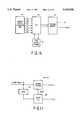
- the present inventionrelates to trellis coded modulation (TCM) transmission and reception systems and particularly concerns the use of TCM in a high definition television (HDTV) application.
- TCMtrellis coded modulation
- Trellis coded modulationis a well known technique for improving the performance of digital transmission and reception systems. Improvements can be achieved in S/N performance at a given power level or alternatively, the transmitted power required to achieve a given S/N performance can be reduced.
- TCMcomprises the use of a multi-state convolution encoder to convert each k input data bits of an input sequence of data bits into k+n output bits, and is therefore referred to as a rate k/(k+n) convolution encoder.
- the output bitsare then mapped into a sequence of discrete symbols (having 2.sup.(k+n) values) of a modulated carrier for data transmission.
- the symbolsmay, for example, comprise 2.sup.(k+n) phase or amplitude values.
- a maximum likelihood decodere.g. a Viterbi decoder
- FIG. 1generally illustrates a system of the type described above.
- Each k bits of an input data streamis converted to k+n output bits by a rate k/(k+n) state-dependent sequential convolution encoder 10.
- Each group of (k+n) output bitsis then mapped to one of 2.sup.(k+n) symbols by a mapper 12.
- the symbolsare transmitted over a selected channel by a transmitter 14.
- a receiverincludes a tuner 16 for converting the signal received over the selected channel to an intermediate frequency signal, which is demodulated by a demodulator 18 to provide a baseband analog signal.
- the analog signalis appropriately sampled by an A/D 20 to recover the transmitted symbols which are then applied to a Viterbi decoder 22 for recovering the original k data bits.
- U.S. Pat. No. 5,087,975discloses a vestigial sideband (VSB) system for transmitting a television signal in the form of successive M-level symbols over a standard 6 MHz television channel.
- the symbol rateis preferably fixed at about 684 H (about 10.76 Mega symbols/sec), where H is the NTSC horizontal scanning frequency.
- This patentalso discloses the use of a receiver comb filter having a feed forward delay of 12 symbol clock intervals for reducing NTSC co-channel interference in the receiver.
- the source datais precoded by a modulo-filter having a feedback delay of 12 symbol clock intervals.
- a complementary modulo postcodermay be used to process the received signal in lieu of the comb filter in the absence of significant NTSC co-channel interference to avoid the degradation of S/N performance attributable thereto.
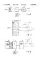
- FIG. 1is a system block diagram of a conventional TCM system employing an optimal MLSE Viterbi decoder
- FIG. 2Ais a system block diagram of a television signal transmitter and receiver including a TCM system employing Viterbi decoding according to the present invention
- FIG. 2Bis a block diagram of an alternate embodiment of the receiver of FIG. 2A;
- FIG. 3illustrates the symbol interleaving effected in the transmitter of FIG. 2;
- FIG. 4is a block diagram illustrating circuits 32 and 34 of FIG. 2 in more detail
- FIG. 5is a diagram illustrating the operation of mapper 49 of FIG. 4;
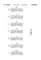
- FIG. 6is a table illustrating the operation of convolution encoder 32b of FIG. 4;
- FIG. 7is a trellis state transition diagram based upon the table of FIG. 6;
- FIG. 8is a block diagram illustrating circuits 42, 44, 46 and 48 of FIG. 2 in more detail
- FIG. 9is a functional block diagram of optimal MLSE Viterbi decoders 46A-46L of FIG. 8;
- FIG. 10is a diagram showing a circuit which may be used in place of Viterbi decoders 46A-46L of FIG. 8 for recovering estimations of bits Y 1 and Y 2 ;
- FIG. 11is a functional block diagram of optimal MLSE Viterbi decoders 44A-44L of FIG. 8;
- FIG. 12is a table illustrating the operation of the TCM encoder of the invention including the effects introduced by comb filter 42 of the receiver of FIG. 2;
- FIGS. 13shows the resultant effect of combining two subsets in comb filter 42 and the resultant cosets that arise
- FIG. 14shows the seven cosets that occur in the table of FIG. 13;
- FIG. 15is a trellis state transition diagram based on the table of FIG. 12;
- FIG. 16is a functional block diagram of a Viterbi decoder programmed on the basis of the trellis diagram of FIG. 15;
- FIG. 17is a block diagram illustrating the use of the Viterbi decoder of FIG. 16 to recover estimations of transmitted bits X 1 and X 2 ;
- FIG. 18illustrates the states of delay elements 48, 54 and 56 of FIG. 4 after a segment sync interval
- FIG. 19illustrates the format of the signal developed at the output of multiplexer 62 of FIG. 4 in the vicinity of a segment sync signal
- FIG. 20is a block diagram of comb filter 42 of FIG. 8 modified for processing data segment and frame sync signals;
- FIG. 21is a block diagram of a postcoder 48A-48L of FIG. 8 modified for processing data segment and frame sync signals;
- FIG. 22illustrates the format of the signal developed at the output of multiplexer 62 of FIG. 4 in the vicinity of a frame sync signal
- FIG. 23illustrates an embodiment of the invention in which an increased bit rate transmission is achieved by providing input data in the form of 3 bits per symbol;
- FIGS. 24A and 24Billustrate the application of the invention to a QAM system
- FIGS. 25A and 25Billustrate respective postcoder configurations useful in receivers for the embodiments of the invention shown in FIGS. 23 and 24.
- FIG. 2Agenerally illustrates a TCM system applied to a multilevel VSB HDTV transmission and reception system of the type disclosed in the '975 patent. While the multilevel VSB HDTV application is contemplated in the preferred embodiment of the invention, it will be understood that the invention is more general in nature and thus may be applied to other types of transmission and reception systems, including lower resolution video systems as well as non-video based data systems. Also, other modulation techniques, such as those employing, for example, quadrature amplitude modulation (QAM) may be employed.
- QAMquadrature amplitude modulation
- a data source 24provides a succession of data bytes which may, for example, comprise a compressed HDTV signal, a compressed television signal of NTSC resolution or any other digital data signal.
- the data bytesare preferably, although not necessarily, arranged in successive frames each including, on an alternating basis, 262 and 263 data segments, each data segment comprising 684 two-bit symbols occurring at a symbol rate of about 10.76M symbols/sec.
- the data bytes from source 24, which also provides a plurality of timing signals,are applied to a Reed-Solomon encoder 26 for forward error correction coding and therefrom to a byte interleaver 28.
- Byte interleaver 28reorders the data bytes throughout a frame to reduce the susceptibility of the system to burst noise.
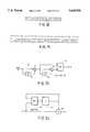
- the interleaved data bytes from interleaver 28are applied to a symbol interleaver 30 which provides in a preferred embodiment two output bit streams X 1 , X 2 at the symbol rate, each bit pair X 1 , X 2 corresponding to a data symbol.
- a symbol interleaver 30which provides in a preferred embodiment two output bit streams X 1 , X 2 at the symbol rate, each bit pair X 1 , X 2 corresponding to a data symbol.
- Each subsegment, e.g. subsegment Athus comprises 57 symbols, e.g. A o -A 56 , separated from each other by 12 symbol intervals.
- Symbol interleaver 30effects such by reordering the applied 2-bit symbols of each data byte as four successive symbols of a respective subsegment.
- the four 2-bit symbols of the first data byte applied to interleaver 30are provided as output symbols A 0 , A 1 , A 2 , and A 3 of subsegment A, the four 2-bit symbols of the second applied data byte as output symbols B o , B 1 , B 2 and B 3 of subsegment B, and so on. This insures that the symbols of each data byte are processed as a unit both in the encoder and the receiver.
- the stream of 2-bit symbols from interleaver 30are coupled to a precoder and trellis encoder 32 for conversion to 3 output bits as will be described in further detail hereinafter.
- unit 32is characterized by a 12-symbol delay, it may be thought of as comprising 12 parallel encoders each operating at 1/12 the symbol clock rate, with each subsegment generated by interleaver 30 being processed by a respective one of the parallel encoders.
- the stream of 3-bit symbols developed at the output of unit 32is applied to a symbol mapper and sync inserter 34 and therefrom to a VSB modulator 36 for transmission as a plurality of 8-level symbols.
- the transmitted signalis received by a receiver including a tuner, demodulator and A/D 40 corresponding to blocks 16, 18 and 20 of FIG. 1.
- the output of unit 40comprises a stream of multibit (e.g. 8-10 bit) 8-level symbols which are applied by components 50a, b, c, and d of a selector switch 50) (see U.S. Pat. No. 5,260,793 for an exemplary embodiment of a circuit for operating switch 50 to a first processing path comprising a comb filter 42 and a first Viterbi decoder 44 and to a second processing path comprising a second Viterbi decoder 46 and a postcoder 48.
- Each of the processing pathsincludes an equalizer 38 coupled between switching components 50b and 50c.
- the outputs of both Viterbi decoder 44 and postcoder 48each comprise reconstructions of bit streams X 1 , X 2 .
- Component 50d of selector switch 50couples one of the applied bit stream pairs X 1 , X 2 to a symbol deinterleaver 52 which reconstructs the original data bytes. These data bytes are then deinterleaved by byte deinterleaver 54 and error-corrected by Reed-Solomon decoder 56 for application to the remainder of the receiver.
- FIG. 2BAn alternate embodiment of the receiver of FIG. 2A is shown in FIG. 2B.
- This embodimentis generally similar to the system of FIG. 2A except that only one Viterbi decoder 45 is provided. More specifically, Viterbi decoder 45 is responsive to a control signal from selector switch 50 for assuming a first configuration for implementing the functions of Viterbi decoder 44 when the first processing path is selected and for assuming a second configuration for implementing the functions of Viterbi decoder 46 when the second processing path is selected.
- unit 32comprises a modulo-2, feedback precoder 32a receiving the symbols (each symbol being identified as bits X 1 , X 2 ) from interleaver 30 for developing output bits Y 1 , Y 2 .
- precoder 32acomprises a modulo-2 summer 44 having a first input connected for receiving bit X 2 and a second input connected to the summer output, which develops output bit Y 2 , by a multiplexer 46 and a 12-symbol delay element 47. The output of delay element 47 is also coupled back to its input by multiplexer 46.
- Output bit Y 2 of summer 44is applied as bit Z 2 to one input of a symbol mapper 49, which is shown in more detail in FIG. 5.
- Uncoded bit Y1 from precoder 32ais applied to a rate 1/2, 4-state, systematic feedback convolution encoder 32b for conversion to output bits Z 1 and Z 0 .
- Convolution encoder 32bcomprises a signal path 51 for applying bit Y 1 directly to a second input of symbol mapper 49 as bit Z 1 and to one input of a modulo-2 summer 52.
- the output of summer 52is applied through a multiplexer 53 to the input of a 12-symbol delay element 54, whose output is applied to a third input of symbol mapper 49 as bit Z 0 and through a second multiplexer 55 to the input of a second 12-symbol delay element 56.
- the output of delay element 56is applied to the second input of summer 52.
- delay elements 54 and 56are also coupled back to their respective inputs by multiplexers 53 and 55.
- Each of the delay elements 47, 54 and 56is clocked at the symbol rate (about 10.76M symbols/sec). It will be appreciated that each subsegment A-L (see FIG. 3) will be independently processed by precoder 32a and convolution encoder 32b on account of the 12-symbol delay elements which characterize their respective operations.
- Convolution encoder 32bmay take various other forms from that shown in FIG. 4 without departing from the invention.
- the number of encoder statesmay differ from that shown, feedforward architectures may be used rather that the disclosed feedback structure and non-systematic coding may be employed in either a feedback or feedforward arrangement.
- Multiplexers 46, 53 and 55are provided to allow for sync insertion during which times their respective B inputs are selected. At all other times the A inputs of the multiplexers are selected.
- the operation of convolution encoder 32b and mapper 49, hereinafter referred to as trellis encoder (TE) 60is illustrated in the table of FIG. 6.
- the first column of the Tablerepresents the four possible states Q 1 Q 0 of the delay elements 56 and 54 of convolution encoder 32b at an arbitrary time n. These states are 00, 01, 10 and 11.
- the second columnrepresents the possible values of bits Y 2 Y 1 for each of the states Q 1 Q 0 of encoder 32b at time n.
- the fourth column of the table, labeled R(n)represents the amplitude of the symbol provided by symbol mapper 49 (see FIG. 5) in response to output bits Z 2 Z 1 Z 0 .
- the 8-level symbols developed at the output of mapper 49are symmetrical around the zero level. To facilitate signal acquisition in the receiver, it is preferred to offset each symbol by a given amount (e.g. +1 unit) to in effect provide a pilot component.
- the symbols and pilot componentare then applied through a multiplexer 62 to modulator 36 (see FIG. 2) where they are used to modulate a selected carrier for transmission in a suppressed carrier VSB form as described in the previously mentioned '975 patent.
- the output of mapper 49is also applied to the input of a RAM 64, whose output is applied to a second input of multiplexer 62.
- a third input of multiplexer 62is supplied from a source 66 of segment and frame sync signals.
- FIG. 7is a state transition diagram for convolution encoder 32b derived from the table of FIG. 6.
- the diagramillustrates the four states of the encoder and the various transitions there between.
- each statehas two parallel branches, each extending to the same or another state.
- the branchesare labeled with the input bits Y 2 Y 1 causing the state transition and the resulting output R of mapper 49.
- this state diagrammay be used to design an optimum maximum likelihood sequence estimation (MLSE) Viterbi decoder in the receiver for recovering estimations of bits Y 2 and Y 1 as is well known in the art.
- MSEmaximum likelihood sequence estimation
- FIG. 8illustrates the receiver decoding aspects of the invention in more detail.
- the multibit symbol values from tuner, demodulator, A/D 40are applied to a first demultiplexer 70 through the first processing path comprising comb filter 42 and equalizer 38 and to a second demultiplexer 72 through the second processing path comprising equalizer 38.
- Comb filter 42comprises a feedforward filter including a linear summer 74 and a 12 symbol delay element 76. As more fully explained in the previously mentioned '975 patent, the filter is operable for reducing NTSC co-channel interference by subtracting from each received symbol, the symbol received 12 symbol intervals earlier.
- the comb filterindependently operates on each of the subsegments for providing successive combed outputs of the form A 1 -A 0 , B 1 -B 0 , etc. These combed outputs are demultiplexed by demultiplexer 70 into 12 separate outputs, each corresponding to a respective one of the subsegments A-L. Each combed subsegment is applied by demultiplexer 70 to a respective Viterbi decoder 44A-44L which is operated at a rate of 1/2 the symbol clock rate (fs).
- Each of the decoders 44A-44Lprovides a pair of output decoded bits comprising estimations of input bits X 1 X 2 , the decoded bits being multiplexed into an interleaved bit stream as shown in FIG. 3 by a multiplexer 78.
- the interleaved symbols from unit 40are also demultiplexed by demultiplexer 72 into the 12 separate subsegments A-L, each being applied to a respective one of the Viterbi decoders 46A-46L. It will thus be seen that each of the original data bytes from source 24 are processed as a unit by a respective one of the decoders 46A-46L. For example, the data byte represented by symbols A 3 A 2 A 1 A 0 is processed by decoder 46A, and so on. The same is of course true for decoders 44A-44L, except that the processed symbols have previously been combed by filter 42.
- Each of the decoders 46A-46Lmay comprise a substantially identical device operating at the rate of fs/12 and programmed according to the state diagram of FIG. 7 for effecting optimum MLSE Viterbi decoding for recovering estimations of bits Y 2 and Y 1 as is well known in the art.
- each of the decoders 46A-46Lis programmed to generate 4 branch metrics, typically using an appropriately programmed ROM, each representing the difference between the received symbol level (i.e. an 8-10 bit value) and the closest one of the two subset levels of each of the symbol subsets a, b, c, and d.
- FIG. 9illustrates a Viterbi decoder manufactured by LSI Logic Corp.
- the decodercomprises a branch metric generator ROM 84 responsive to the received symbols for generating and applying 4 branch metrics to an add, compare and select (ACS) unit 86.
- ACS unit 86is bidirectionally coupled to a path metric storage memory 88 and also supplies a traceback memory 90.
- ACS unit 86adds the branch metrics generated by generator 84 to the previous path metrics stored in memory 88 to generate new path metrics, compares the path metrics emanating from the same states and selects the ones with the lowest path metrics for storage.
- Traceback memory 90after a number of branches have been developed, is operable for selecting a surviving path and generating estimations of the bits Y 2 and Y 1 that would have produced the surviving path.
- each Viterbi decoder 46A-46L in FIG. 8comprises only an estimation of bit Y 2 , not input but X 2 . Consequently, a complementary modulo-2 postcoder 48A-48L is used in the receiver to recover estimations of input bits X 1 and X 2 from each respective decoder 46A-46L.
- Each postcoder 48A-48Lcomprises a direct path between input bit Y 1 and output bit X 1 and a feedforward circuit in which output bit Y 2 is applied directly to one input of a modulo-2 adder 92 and to a second input of adder 92 via a one-symbol delay element 94.
- the output of adder 92comprises an estimation of input bit X 2 .
- the decoded bits X 1 , X 2 from postcoders 48A-48Lare multiplexed into an interleaved bit stream as shown in FIG. 3 by a multiplexer 96.
- each of the Viterbi decoders 46A-46Lmay be replaced by a slicer 98 as illustrated in FIG. 10 to provide a cost reduced receiver in cases where the received signal is characterized by a relatively high S/N ratio. This is frequently the case in cable transmissions which normally exhibit a better S/N ratio than terrestrial transmissions. A tradeoff is therefore made between TCM coding gain and receiver complexity and cost.
- slicer 98is characterized by three slice levels (-4, 0 and +4).
- bits Y 2 Y 1are converted to an estimation of bits X 2 X 1 by a respective postcoder 48A-48L.
- slicer 98effects proper decoding of the received symbols because successive symbol levels are represented by common values of bits Z 2 Z 1 , as previously mentioned.
- This embodiment of the inventiontherefore, in effect, implements a 4-level transmission and reception system which provides an equivalent bit rate as the 8-level TCM system, but with worse S/N performance since the TCM coding gain is not realized.
- comb filter 42has the desired affect of reducing NTSC co-channel interference, it also increases the complexity of decoders 44A-44L where optimum MLSE Viterbi decoding is used to recover bits X 1 and X 2 .
- an optimum MLSE Viterbi decodermust take into account not only the state of the encoder, but also the state of delay element 76 of comb filter 42. Since there are 4 encoder states and 4 possible ways to enter each state (i.e. there are 4 possible states of delay element 76 for each state of encoder 32b), an optimum decoder must process a 16-state trellis.
- the decodermust account for 4 branches entering each state whereas only 2 branches enter each encoder state.
- Such a decoderis illustrated in FIG. 11 and, while complex in nature, its design is relatively straight forward.
- the functionality of the decoderis similar to that shown in FIG. 9 (the same reference numerals are therefore used), its complexity is greatly increased including the requirement to generate 15 branch metrics instead of just 4.
- the branch metricsrepresent the difference between a received symbol level and each of the possible 15 constellation points at the output of comb filter 42 (i.e. the linear combination of the 8-level symbols provides 15 possible output levels).
- the table of FIG. 12illustrates a technique according to the invention for reducing the complexity, and thereby the cost, of the Viterbi decoders 44A-44L used to recover bits X 1 and X 2 from the output of comb filter 42.
- This simplificationwhich is made possible by precoding bit X 2 as shown in FIG. 4, is achieved by ignoring some of the state information from delay element 76 of comb filter 42 in constructing the trellis diagram forming the basis of the decoder.
- decoding simplificationis achieved according to this aspect of the invention by considering only the information identifying the subsets a, b, c and d of the 8 possible states of delay element 76 of the comb filter.
- the first columnrepresents the state of the combined encoder and channel (using only subset information to represent the state of delay element 76) Q 1 Q 0 V 1 V 0 at time n.
- These eight statesare derived from the last two columns of the table of FIG. 6 which gives the states Q 1 Q 0 of encoder 32b and the associated V 1 V 0 subset of the output V of delay element 76 at an arbitrary time (n+1).
- V 1 V 0 subset at time (n+1)is the same as output bits Z 1 Z 0 at time n (see the third column of the FIG. 6 table).
- Each state Q 1 Q 0 V 1 V 0 of the combined encoder and channelis listed twice in the table of FIG. 12, once for each possible value of input bit X 1 (see the third column of the table).
- the fourth column of the tablerepresents the subset Z 1 Z 0 at time n for each encoder/channel state and each value of input bit X 1 .
- Both the V 1 V 0 subset in the first column of the table and the Z 1 Z 0 subset comprising the fourth column of the tableare identified by the subset identifiers (a-d) shown in mapper 49 of FIG. 5 in the second and fifth columns respectively of the table.
- the output of linear summer 74 of comb filter 42 applied to each decoder 44A-44Lis identified by the letter U and comprises the value of a received symbol minus the value of the previous symbol.
- This valueis represented in the sixth column of the table of FIG. 12 as the difference between the Z subset Z 1 Z 0 and the V subset V 1 V 0 in terms of the subset identifiers (a-d).
- the U subset at time n for the first row of the tableis (d--d), for the fifth row (c-d), and so on.
- each possible Z subsetis identified along the top of the Figure by the darkened circles corresponding to the levels of the respective subsets.
- subset acomprises levels -1 and +7 of the 8 levels
- subset bcomprises levels -3 and +5, and so on.
- the U subset (a--a), see the last row of the table of FIG. 12,is derived by subtracting the a subset levels -1 and +7 from the a subset levels -1 and +7, which gives the three levels +8, 0, -8 as shown in the upper left-hand corner of FIG. 13.
- the U subset (a-b), see the 8th row of the FIG. 12 tableis derived by subtracting the b subset levels -3 and +5 from the a subset levels -1 and +7, which gives the three levels +10, +2, -6 as shown, and so on.
- cosetsExamination of the 16 U subsets shown in FIG. 13 reveals that each belongs to one of 7 common subsets hereinafter referred to as cosets. These 7 cosets are shown in FIG. 14 and identified as cosets A (U subsets a--a, b--b, c--c and d--d), B1 (U subsets b-a, c-b and d-c), B2 (U subset a-d), Cl (U subsets c-a and d-b), C2 (U subsets a-c and b-d), D1 (U subset d-a) and D2 (U subsets a-b, b-c and c-d).
- the coset for each U subsetis also shown in the 7th column of the table of FIG. 12. It will be observed that each coset comprises 3 of 15 possible levels.
- the final column of the table of FIG. 12, which corresponds to the last two columns of the table of FIG. 6,represents the state Q 1 Q 0 V 1 V 0 of the encoder/channel at time (n+1).
- the first and last columns of the tablecan now be used to construct a trellis state transition diagram for the combined encoder/channel as shown in FIG. 15.
- V 0has been disregarded since it is redundant with Q 1 .
- the trellis state transition diagramthus comprises 8 states, with two branches emanating from each state. Each branch is labeled with the input bit X 1 and the coset A, B1, B2, C1, C2, D1 and D2 associated with the respective transition.
- This decoderwhich comprises an alternate embodiment of the optimum Viterbi decoder of FIG. 11, may take the form of the Viterbi decoder illustrated in FIG. 16.
- the apparatus used to implement this Viterbi decodermay be similar to that used in the decoder of FIGS. 9 and 11 and thus comprises a branch metric generator 84, an ACS unit 86, a path metric storage memory 88 and a traceback memory 90. In the case of the decoder of FIG.
- the foregoing characteristicsare used to estimate bit X 2 as shown in FIG. 17.
- the symbol level U at the output of summer 74 of comb filter 42is applied through a delay 100 (chosen to match the delay of Viterbi decoders 44A-44L) to one input of a plurality, i.e. 7, of slicers 102.
- the coset identification signal at the output of Viterbi decoder 44A-44Lis applied to the second input of slicer 102.
- An estimation of bit X 2is developed by slicer 102 by determining whether the U symbol level from comb filter 42 is closer to one of the outer levels (e.g.
- precoder 32ain the path of input bit X 2 requires the incorporation of a complementary postcoder 104 in the path of estimated bit X 2 when an optimal MLSE Viterbi decoder is used to process the output of comb filter 42 as shown in FIG. 11.
- a complementary postcoderis not required in the case of the circuit of FIG. 17 since estimated bit X 2 is directly produced.
- the data provided by source 24is preferably arranged in successive data frames, each comprising, a plurality of data segments of 684 symbols, although the following aspects of the invention are equally applicable to arrangements having different numbers of data segments per frame and different numbers of symbols per data segment. It is further desirable to incorporate a frame sync signal, which may comprise one or more pseudo-random sequences, in the first data segment of each frame and a data segment sync signal in the first four symbol positions of each data segment. Referring back to FIG. 4, the frame and segment sync signals are inserted at the appropriate times into the data stream at the output of multiplexer 62 by frame and data segment sync generator 66.
- the B input of multiplexer 46 of precoder 32a and the B inputs of multiplexers 53 and 55 of convolution encoder 32bare selected. Also, the last 12 symbols of the last data segment of each frame are read into memory 64 and copied into the last 12 symbol intervals of the frame sync segment at the output of multiplexer 62. As will be explained in further detail hereinafter, the foregoing provisions are effective to insure that in the receiver symbols from each of the subsegments A-L (see FIG. 3) are only processed with symbols from the same subsegment.
- each of the delay elementswill be characterized as shown in FIG. 18 immediately following the segment sync interval, wherein the state of the delay elements is defined by a symbol from subsegment E.
- the composite signal in the vicinity of the segment sync signal S 0 , S 1 , S 2 and S 3is illustrated in FIG.
- FIG. 20shows an embodiment of comb filter 42 of FIG. 8 modified for operation in accordance with the sync insertion aspects of the invention.
- the modificationcomprises the provision of a multiplexer 110 having an A input for directly receiving the output of the comb filter and a B input for receiving the output of a summer 112.
- One input of summer 112is connected directly to the output of the comb filter while its second input is connected to the comb filter output by a 12-symbol delay element 114.
- the B input of multiplexer 110is selected during symbol intervals 13-16 (i.e. the sync interval delayed by 12 symbol clocks) and otherwise the A input is selected.
- the output of comb filter 42 during the sync intervalcomprises:
- This informationwhich is applied to the decoder via the A input of multiplexer 110, does not represent meaningful data and is therefore ignored by the decoder.
- symbols from the same subsegmentsare properly combed together and provided to the decoder via the A input of multiplexer 110.
- the B input of multiplexer 110is selected.
- the output of comb filter 42 during this periodis:
- each outputrepresents combed data symbols from the same subsegment as desired. Thereafter, the A input of multiplexer 110 is again selected and normal processing continues.
- FIG. 21shows an embodiment of the postcoders used in the receiver of the invention, see, for example, postcoders 48A-48L of FIG. 8 and 10, modified for operation in accordance with the sync insertion aspects of the invention.
- the modified postcoderwhich comprises a modulo adder 120 and a feedforward delay 122, further includes a multiplexer 124 for coupling the output of delay 122 back to its input during the sync interval and otherwise applying the postcoder input signal to an input of adder 120 through delay 122.
- each of the modified postcoder 48A-48Lwill have stored in its respective delay 122 the symbol from the subsegment with which it is associated as desired.
- Frame sync insertion and processingis effected much in the same manner as described above in connection with data segment sync. More specifically, during the frame sync interval, i.e. the first data segment of each frame, generator 66 and multiplexer 62 are initially operated for inserting frame sync symbols V 0 -V 671 into the first 672 symbol positions of the frame sync segment S 0 as shown in FIG. 22. The last 12 symbols of the frame sync segment are inserted into the data stream by RAM 64 and comprise the last 12 symbols of the last data segment S312 of the previous frame (which had previously been written into RAM 64). Also, since the B inputs of multiplexers 46, 53 and 55 are selected during the frame sync interval, delay elements 48, 54 and 56 will assume the condition shown in FIG. 18 at the end of the segment sync interval of the next data segment S 1 , which will then be formed as previously described and as shown in FIG. 22.
- FIGS. 20 and 21operate as previously described to insure that symbols from each of the subsegments A-L are processed with symbols only of the same subsegment.
- the outputs of the two circuits during the frame sync segment S 0do not represent meaningful data and are therefore ignored during subsequent processing.
- FIG. 23illustrates an application of the invention to a system wherein each symbol represents 3 bits instead of 2 bits as previously described.
- input data bits X 1 , X 2 and X 3are provided at the symbol rate, bits X 3 and X 2 being converted by a modulo 4 precoder 32a' which includes a modulo 4 combiner 44', to bits Y 3 and Y 2 for application as bits Z 3 and Z 2 to a 16-level symbol mapper 491.
- Data bit X 1is applied as bit Z 1 to a third input of mapper 491 and to convolution encoder 32b which develops bit Z 0 for application to the fourth input of mapper 491.
- bits Z 1 Z 0identify subsets a, b, c, and d, each of which comprises 4 symbol levels. Also, within each subset the respective symbol amplitudes differ by a magnitude of 8 units and successive symbol levels (e.g. -15, -13) are selected by common states of bits Z 3 Z 2 Z 1 .
- the signal generated by the circuit of FIG. 23may therefore be decoded using the techniques previously described. In this example, an optimum MLSE decoder (i.e.
- the precoderone that does not take into account the precoder and is used to decode the output of the comb filter) would have 8 times the number of states that the encoder has.
- the inclusion of the modulo-4 precoderallows the decoder to operate on a trellis that has only twice as many states as the encoder and still decode the uncoded bits without error propagation.
- FIGS. 24A and 24Billustrate the application of the invention to a QAM modulator.
- 3 inputs bits X 1 , X 2 and X 3are provided, bits X 3 and X 2 being independently precoded by respective modulo-2 precoders 32 11 a and 32 111 a to provide output bits Z 3 and Z 2 and bit X 1 being supplied to convolution encoder 32b for generating output bits Z 1 and Z 0 .
- Output bits Z 3 Z 2 Z 1 Z 0are applied to a symbol mapper 49 11 for generating 16 quadrature related symbols (see FIG. 24B) belonging to one of the subsets a-d for application to a QAM modulator 36 1 .
- bits Z 1 Z 0identify the respective symbol subset a-d.
- Receivers for the systems of FIGS. 23 and 24may take the form generally illustrated in FIG. 8.
- a modulo 4 postcoder 48A'including a modulo 4 combiner 92' as shown in FIG. 25A would replace each modulo 2 postcoder 48A and, in the case of the system of FIGS. 24A and B, a pair of modulo 2 postcoders 48A" and 48A"' as shown in FIG. 25B would replace each modulo 2 postcoder 48A.
Landscapes
- Engineering & Computer Science (AREA)
- Signal Processing (AREA)
- Computer Networks & Wireless Communication (AREA)
- Multimedia (AREA)
- Artificial Intelligence (AREA)
- Error Detection And Correction (AREA)
- Digital Transmission Methods That Use Modulated Carrier Waves (AREA)
- Television Systems (AREA)
- Synchronisation In Digital Transmission Systems (AREA)
- Synchronizing For Television (AREA)
- Television Signal Processing For Recording (AREA)
- Compression Or Coding Systems Of Tv Signals (AREA)
Abstract
Description
Claims (16)
Priority Applications (8)
| Application Number | Priority Date | Filing Date | Title |
|---|---|---|---|
| US08/272,357US5629958A (en) | 1994-07-08 | 1994-07-08 | Data frame structure and synchronization system for digital television signal |
| KR1019970700046AKR100274288B1 (en) | 1994-07-08 | 1995-06-29 | Data frame composition method and receiver |
| CA002194354ACA2194354C (en) | 1994-07-08 | 1995-06-29 | Data frame structure and synchronization system for digital television signal |
| BR9508262ABR9508262A (en) | 1994-07-08 | 1995-06-29 | Process of structuring a data frame and receiver |
| CNB951939823ACN1166192C (en) | 1994-07-08 | 1995-06-29 | Data frame structure and synchronization system for digital television signal |
| JP50432796AJP3386136B2 (en) | 1994-07-08 | 1995-06-29 | Data frame structure and synchronization system for digital television signals |
| PCT/US1995/008135WO1996002108A1 (en) | 1994-07-08 | 1995-06-29 | Data frame structure and synchronization system for digital television signal |
| MX9700153AMX9700153A (en) | 1994-07-08 | 1995-06-29 | Data frame structure and synchronization system for digital television signal. |
Applications Claiming Priority (1)
| Application Number | Priority Date | Filing Date | Title |
|---|---|---|---|
| US08/272,357US5629958A (en) | 1994-07-08 | 1994-07-08 | Data frame structure and synchronization system for digital television signal |
Publications (1)
| Publication Number | Publication Date |
|---|---|
| US5629958Atrue US5629958A (en) | 1997-05-13 |
Family
ID=23039452
Family Applications (1)
| Application Number | Title | Priority Date | Filing Date |
|---|---|---|---|
| US08/272,357Expired - LifetimeUS5629958A (en) | 1994-07-08 | 1994-07-08 | Data frame structure and synchronization system for digital television signal |
Country Status (8)
| Country | Link |
|---|---|
| US (1) | US5629958A (en) |
| JP (1) | JP3386136B2 (en) |
| KR (1) | KR100274288B1 (en) |
| CN (1) | CN1166192C (en) |
| BR (1) | BR9508262A (en) |
| CA (1) | CA2194354C (en) |
| MX (1) | MX9700153A (en) |
| WO (1) | WO1996002108A1 (en) |
Cited By (36)
| Publication number | Priority date | Publication date | Assignee | Title |
|---|---|---|---|---|
| US5933462A (en)* | 1996-11-06 | 1999-08-03 | Qualcomm Incorporated | Soft decision output decoder for decoding convolutionally encoded codewords |
| WO2000041396A1 (en)* | 1999-01-07 | 2000-07-13 | Packetvideo Corporation | Method and device for robust decoding of header information in macroblock-based compressed video data |
| US6091742A (en)* | 1998-08-17 | 2000-07-18 | Gilant Satellite Networks Ltd. | Bi-directional communications protocol |
| US6122010A (en)* | 1996-12-16 | 2000-09-19 | Vidicast Ltd. | Television signal data transmission system |
| US6184921B1 (en)* | 1998-02-20 | 2001-02-06 | Samsung Electronics Co., Ltd. | Method for transmitting VSB digital TV with carrier frequency near co-channel NTSC audio carrier frequency |
| US6201563B1 (en)* | 1998-06-08 | 2001-03-13 | Lsi Logic Corporation | Trellis code modulation decoder structure for advanced digital television receiver |
| US6212654B1 (en) | 1997-07-22 | 2001-04-03 | Lucent Technologies Inc. | Coded modulation for digital storage in analog memory devices |
| US6363130B1 (en)* | 1997-10-10 | 2002-03-26 | Nortel Networks Limited | Detection of access bursts in TDMA communications systems |
| US20020041634A1 (en)* | 2000-10-02 | 2002-04-11 | Lg Electronics Inc. | VSB Transmission system |
| US6388701B1 (en)* | 1998-05-07 | 2002-05-14 | Samsung Electronics Co., Ltd. | Device and method for removing co-channel interference signal in modulation/demodulation receiver having reference signal |
| US20020085632A1 (en)* | 2000-12-28 | 2002-07-04 | Lg Electronics, Inc. | VSB transmission system for processing supplemental transmission data |
| US20020126222A1 (en)* | 2001-01-19 | 2002-09-12 | Lg Electronics, Inc. | VSB reception system with enhanced signal detection for processing supplemental data |
| US20020140867A1 (en)* | 2001-03-30 | 2002-10-03 | Weiss S. Merrill | Digital signal transmitter synchronization system |
| US20020154709A1 (en)* | 2001-04-20 | 2002-10-24 | Lg Electronics Inc. | Digital VSB transmission system |
| US20020159520A1 (en)* | 2001-04-25 | 2002-10-31 | Lg Electronics Inc. | Communication system in digital television |
| US20020172277A1 (en)* | 2001-04-18 | 2002-11-21 | Lg Electronics, Inc. | VSB communication system |
| US20020181599A1 (en)* | 2001-04-25 | 2002-12-05 | Lg Electronics Inc. | Communication system in digital television |
| US6493402B1 (en)* | 1999-05-27 | 2002-12-10 | Zenith Electronics Corporation | Mode control for trellis decoder |
| US20020186780A1 (en)* | 2001-06-11 | 2002-12-12 | Lg Electronics Inc. | Digital VSB transmission system |
| US20020186790A1 (en)* | 2001-06-11 | 2002-12-12 | Lg Electronics Inc. | Digital VSB transmission system |
| US6603824B1 (en)* | 1998-04-08 | 2003-08-05 | Robert Bosch Gmbh | Method for demodulating a carrier wave modulated by a digital symbol sequence |
| US6668014B1 (en)* | 1999-12-09 | 2003-12-23 | Ati Technologies Inc. | Equalizer method and apparatus using constant modulus algorithm blind equalization and partial decoding |
| US20040090997A1 (en)* | 2001-08-20 | 2004-05-13 | Lg Electronics Inc. | Digital transmission system with enhanced data multiplexing in VSB transmission system |
| US20040207757A1 (en)* | 2000-04-18 | 2004-10-21 | Mark Fimoff | Mapping arrangement for digital communication system |
| US20050041749A1 (en)* | 2000-09-26 | 2005-02-24 | Lg Electronics Inc. | Digital television system |
| US20050111586A1 (en)* | 2003-11-04 | 2005-05-26 | Lg Electronics Inc. | Digital E8-VSB reception system and E8-VSB data demultiplexing method |
| US20050141606A1 (en)* | 2001-04-18 | 2005-06-30 | Lg Electronics Inc. | VSB communication system |
| US7148932B2 (en) | 2000-09-22 | 2006-12-12 | Lg Electronics Inc. | Communication system in digital television |
| US20090052588A1 (en)* | 2006-02-16 | 2009-02-26 | Wen Gao | Apparatus and Method for Sensing an Atsc Signal in Low Signal-to-Noise Ratio |
| US20090153748A1 (en)* | 2005-11-04 | 2009-06-18 | Wen Gao | Apparatus and Method for Sensing an ATSC Signal in Low Signal-To-Noise Ratio |
| US20090232759A1 (en)* | 2005-12-16 | 2009-09-17 | Fraser Ian Bell | Hair Treatment Compositions |
| US20100232495A1 (en)* | 2007-05-16 | 2010-09-16 | Citta Richard W | Apparatus and method for encoding and decoding signals |
| US20100296576A1 (en)* | 2007-10-15 | 2010-11-25 | Thomson Licensing | Preamble for a digital television system |
| US20110145678A1 (en)* | 2009-12-10 | 2011-06-16 | Rajat Agarwal | Data line storage and transmission utilizing both error correcting code and synchronization information |
| US8908773B2 (en) | 2007-10-15 | 2014-12-09 | Thomson Licensing | Apparatus and method for encoding and decoding signals |
| US10361715B1 (en)* | 2018-06-04 | 2019-07-23 | Amazon Technologies, Inc. | Decompression circuit |
Families Citing this family (3)
| Publication number | Priority date | Publication date | Assignee | Title |
|---|---|---|---|---|
| US5398073A (en)* | 1994-04-12 | 1995-03-14 | At&T Corp. | Concatenated coded vestigial sideband modulation for high definition television |
| US5841478A (en)* | 1996-04-09 | 1998-11-24 | Thomson Multimedia, S.A. | Code sequence detection in a trellis decoder |
| DE69739878D1 (en)* | 1996-04-09 | 2010-07-01 | Thomson Multimedia Sa | Detection of a Code Sequence in a Trellis Decoder |
Citations (8)
| Publication number | Priority date | Publication date | Assignee | Title |
|---|---|---|---|---|
| EP0422443A2 (en)* | 1989-10-13 | 1991-04-17 | Alcatel SEL Aktiengesellschaft | Multiplexer and demultiplexer, especially for information transmission networks with a synchronous hierarchy of digital signals |
| US5087975A (en)* | 1990-11-09 | 1992-02-11 | Zenith Electronics Corporation | VSB HDTV transmission system with reduced NTSC co-channel interference |
| US5222077A (en)* | 1991-04-09 | 1993-06-22 | Racal-Datacom, Inc. | Radix mapping with variable number of symbols in mapping period |
| US5260793A (en)* | 1991-07-18 | 1993-11-09 | Zenith Electronics Corporation | Receiver post coder selection circuit |
| US5311554A (en)* | 1992-07-02 | 1994-05-10 | Motorola, Inc. | Synchronized offset extraction in a data receiver |
| US5321725A (en)* | 1991-07-26 | 1994-06-14 | General Instrument Corporation | Method and apparatus for communicating digital information such as compressed video using treillis coded QAM |
| US5341401A (en)* | 1991-09-10 | 1994-08-23 | Telefonaktiebolaget L M Ericsson | Method of detecting the channel identity of a number of channels in a mobile radio system |
| US5442646A (en)* | 1994-02-01 | 1995-08-15 | The Mitre Corporation | Subcarrier communication system |
- 1994
- 1994-07-08USUS08/272,357patent/US5629958A/ennot_activeExpired - Lifetime
- 1995
- 1995-06-29CNCNB951939823Apatent/CN1166192C/ennot_activeExpired - Lifetime
- 1995-06-29WOPCT/US1995/008135patent/WO1996002108A1/enactiveIP Right Grant
- 1995-06-29MXMX9700153Apatent/MX9700153A/enunknown
- 1995-06-29BRBR9508262Apatent/BR9508262A/ennot_activeIP Right Cessation
- 1995-06-29KRKR1019970700046Apatent/KR100274288B1/ennot_activeExpired - Lifetime
- 1995-06-29JPJP50432796Apatent/JP3386136B2/ennot_activeExpired - Lifetime
- 1995-06-29CACA002194354Apatent/CA2194354C/ennot_activeExpired - Lifetime
Patent Citations (8)
| Publication number | Priority date | Publication date | Assignee | Title |
|---|---|---|---|---|
| EP0422443A2 (en)* | 1989-10-13 | 1991-04-17 | Alcatel SEL Aktiengesellschaft | Multiplexer and demultiplexer, especially for information transmission networks with a synchronous hierarchy of digital signals |
| US5087975A (en)* | 1990-11-09 | 1992-02-11 | Zenith Electronics Corporation | VSB HDTV transmission system with reduced NTSC co-channel interference |
| US5222077A (en)* | 1991-04-09 | 1993-06-22 | Racal-Datacom, Inc. | Radix mapping with variable number of symbols in mapping period |
| US5260793A (en)* | 1991-07-18 | 1993-11-09 | Zenith Electronics Corporation | Receiver post coder selection circuit |
| US5321725A (en)* | 1991-07-26 | 1994-06-14 | General Instrument Corporation | Method and apparatus for communicating digital information such as compressed video using treillis coded QAM |
| US5341401A (en)* | 1991-09-10 | 1994-08-23 | Telefonaktiebolaget L M Ericsson | Method of detecting the channel identity of a number of channels in a mobile radio system |
| US5311554A (en)* | 1992-07-02 | 1994-05-10 | Motorola, Inc. | Synchronized offset extraction in a data receiver |
| US5442646A (en)* | 1994-02-01 | 1995-08-15 | The Mitre Corporation | Subcarrier communication system |
Cited By (155)
| Publication number | Priority date | Publication date | Assignee | Title |
|---|---|---|---|---|
| US5933462A (en)* | 1996-11-06 | 1999-08-03 | Qualcomm Incorporated | Soft decision output decoder for decoding convolutionally encoded codewords |
| US6122010A (en)* | 1996-12-16 | 2000-09-19 | Vidicast Ltd. | Television signal data transmission system |
| US6212654B1 (en) | 1997-07-22 | 2001-04-03 | Lucent Technologies Inc. | Coded modulation for digital storage in analog memory devices |
| US6363130B1 (en)* | 1997-10-10 | 2002-03-26 | Nortel Networks Limited | Detection of access bursts in TDMA communications systems |
| US6184921B1 (en)* | 1998-02-20 | 2001-02-06 | Samsung Electronics Co., Ltd. | Method for transmitting VSB digital TV with carrier frequency near co-channel NTSC audio carrier frequency |
| US6603824B1 (en)* | 1998-04-08 | 2003-08-05 | Robert Bosch Gmbh | Method for demodulating a carrier wave modulated by a digital symbol sequence |
| US6388701B1 (en)* | 1998-05-07 | 2002-05-14 | Samsung Electronics Co., Ltd. | Device and method for removing co-channel interference signal in modulation/demodulation receiver having reference signal |
| US6201563B1 (en)* | 1998-06-08 | 2001-03-13 | Lsi Logic Corporation | Trellis code modulation decoder structure for advanced digital television receiver |
| US6091742A (en)* | 1998-08-17 | 2000-07-18 | Gilant Satellite Networks Ltd. | Bi-directional communications protocol |
| US6356661B1 (en) | 1999-01-07 | 2002-03-12 | M4 Labs, Inc | Method and device for robust decoding of header information in macroblock-based compressed video data |
| WO2000041396A1 (en)* | 1999-01-07 | 2000-07-13 | Packetvideo Corporation | Method and device for robust decoding of header information in macroblock-based compressed video data |
| US6493402B1 (en)* | 1999-05-27 | 2002-12-10 | Zenith Electronics Corporation | Mode control for trellis decoder |
| US6668014B1 (en)* | 1999-12-09 | 2003-12-23 | Ati Technologies Inc. | Equalizer method and apparatus using constant modulus algorithm blind equalization and partial decoding |
| US6958781B2 (en)* | 2000-04-18 | 2005-10-25 | Zenith Electronics Corporation | Mapping arrangement for digital communication system |
| US7277505B2 (en) | 2000-04-18 | 2007-10-02 | Zenith Electronics Corporation | Mapping arrangement for digital communication system |
| US20040207757A1 (en)* | 2000-04-18 | 2004-10-21 | Mark Fimoff | Mapping arrangement for digital communication system |
| US7148932B2 (en) | 2000-09-22 | 2006-12-12 | Lg Electronics Inc. | Communication system in digital television |
| US7706449B2 (en) | 2000-09-26 | 2010-04-27 | Lg Electronics Inc. | Digital television system |
| US7474703B2 (en) | 2000-09-26 | 2009-01-06 | Lg Electronics Inc. | Digital television system |
| US7474702B2 (en) | 2000-09-26 | 2009-01-06 | Lg Electronics Inc. | Digital television system |
| US20080056388A1 (en)* | 2000-09-26 | 2008-03-06 | Choi In H | Digital television system |
| US9756334B2 (en) | 2000-09-26 | 2017-09-05 | Lg Electronics Inc. | Digital television system |
| US7742530B2 (en) | 2000-09-26 | 2010-06-22 | Lg Electronics Inc. | Digital television system |
| US20100275095A1 (en)* | 2000-09-26 | 2010-10-28 | In Hwan Choi | Digital television system |
| US8428150B2 (en) | 2000-09-26 | 2013-04-23 | Lg Electronics Inc. | Digital television system |
| US8743971B2 (en) | 2000-09-26 | 2014-06-03 | Lg Electronics Inc. | Digital television system |
| US20050129132A1 (en)* | 2000-09-26 | 2005-06-16 | Lg Electronics Inc. | Digital television system |
| US20050089103A1 (en)* | 2000-09-26 | 2005-04-28 | Lg Electronics Inc. | Digital television system |
| US20050041748A1 (en)* | 2000-09-26 | 2005-02-24 | Lg Electronics Inc. | Digital television system |
| US20050041749A1 (en)* | 2000-09-26 | 2005-02-24 | Lg Electronics Inc. | Digital television system |
| US20100017689A1 (en)* | 2000-10-02 | 2010-01-21 | In Hwan Choi | Vsb transmission system |
| US7577208B2 (en) | 2000-10-02 | 2009-08-18 | Lg Electronics Inc. | VSB transmission system |
| US20070248187A1 (en)* | 2000-10-02 | 2007-10-25 | In Hwan Choi | Vsb transmission system |
| US7298786B2 (en) | 2000-10-02 | 2007-11-20 | Lg Electronics, Inc. | VSB transmission system |
| US7894549B2 (en) | 2000-10-02 | 2011-02-22 | Lg Electronics Inc. | VSB transmission system |
| US20100007785A1 (en)* | 2000-10-02 | 2010-01-14 | In Hwan Choi | Vsb transmission system |
| US7460606B2 (en) | 2000-10-02 | 2008-12-02 | Lg Electronics, Inc. | VSB transmission system |
| US20050074069A1 (en)* | 2000-10-02 | 2005-04-07 | Lg Electronics Inc. | VSB transmission system |
| US20050078760A1 (en)* | 2000-10-02 | 2005-04-14 | Lg Electronics Inc. | VSB transmission system |
| US8320485B2 (en) | 2000-10-02 | 2012-11-27 | Lg Electronics Inc. | VSB transmission system |
| US7613246B2 (en) | 2000-10-02 | 2009-11-03 | Lg Electronics Inc. | VSB transmission system |
| US20020041634A1 (en)* | 2000-10-02 | 2002-04-11 | Lg Electronics Inc. | VSB Transmission system |
| US8059718B2 (en) | 2000-12-28 | 2011-11-15 | Lg Electronics Inc. | VSB transmission system for processing supplemental transmission data |
| US20040184547A1 (en)* | 2000-12-28 | 2004-09-23 | Lg Electronics Inc. | VSB transmission system for processing supplemental transmission data |
| US8130833B2 (en) | 2000-12-28 | 2012-03-06 | Lg Electronics Inc. | VSB transmission system for processing supplemental transmission data |
| US20040179621A1 (en)* | 2000-12-28 | 2004-09-16 | Lg Electronics Inc. | VSB transmission system for processing supplemental transmission data |
| US7539247B2 (en)* | 2000-12-28 | 2009-05-26 | Lg Electronics Inc. | VSB transmission system for processing supplemental transmission data |
| US7522666B2 (en)* | 2000-12-28 | 2009-04-21 | Lg Electronics Inc. | VSB transmission system for processing supplemental transmission data |
| US20050089095A1 (en)* | 2000-12-28 | 2005-04-28 | Lg Electronics Inc. | VSB transmission system for processing supplemental transmission data |
| US20020085632A1 (en)* | 2000-12-28 | 2002-07-04 | Lg Electronics, Inc. | VSB transmission system for processing supplemental transmission data |
| US7616688B2 (en) | 2000-12-28 | 2009-11-10 | Lg Electronics Inc. | VSB transmission system for processing supplemental transmission data |
| US7430251B2 (en) | 2000-12-28 | 2008-09-30 | Lg Electronics Inc. | VSB transmission system for processing supplemental transmission data |
| US7346107B2 (en) | 2000-12-28 | 2008-03-18 | Lg Electronics, Inc. | VSB transmission system for processing supplemental transmission data |
| US20040187055A1 (en)* | 2000-12-28 | 2004-09-23 | Lg Electronics Inc. | VSB transmission system for processing supplemental transmission data |
| US20040184469A1 (en)* | 2000-12-28 | 2004-09-23 | Lg Electronics Inc. | VSB transmission system for processing supplemental transmission data |
| US7010038B2 (en) | 2000-12-28 | 2006-03-07 | Lg Electronics Inc. | VSB transmission system for processing supplemental transmission data |
| US7319495B2 (en)* | 2001-01-19 | 2008-01-15 | Lg Electronics Inc. | VSB reception system with enhanced signal detection for processing supplemental data |
| US7755704B2 (en) | 2001-01-19 | 2010-07-13 | Lg Electronics Inc. | VSB reception system with enhanced signal detection for processing supplemental data |
| US7068326B2 (en) | 2001-01-19 | 2006-06-27 | Lg Electronics Inc. | VSB reception system with enhanced signal detection for processing supplemental data |
| US20100278274A1 (en)* | 2001-01-19 | 2010-11-04 | Lg Electronics Inc. | Vsb reception system with enhanced signal detection for processing supplemental data |
| US7619689B2 (en)* | 2001-01-19 | 2009-11-17 | Lg Electronics Inc. | VSB reception system with enhanced signal detection for processing supplemental data |
| US20040179612A1 (en)* | 2001-01-19 | 2004-09-16 | Lg Electronics Inc | VSB reception system with enhanced signal detection for processing supplemental data |
| US7911539B2 (en) | 2001-01-19 | 2011-03-22 | Lg Electronics Inc. | VSB reception system with enhanced signal detection for processing supplemental data |
| US20060203127A1 (en)* | 2001-01-19 | 2006-09-14 | Lg Electronics Inc. | VSB reception system with enhanced signal detection for processing supplemental data |
| US20040179614A1 (en)* | 2001-01-19 | 2004-09-16 | Lg Electronics Inc. | VSB reception system with enhanced signal detection for processing supplemental data |
| US7787053B2 (en) | 2001-01-19 | 2010-08-31 | Lg Electronics Inc. | VSB reception system with enhanced signal detection for processing supplemental data |
| US6760077B2 (en)* | 2001-01-19 | 2004-07-06 | Lg Electronics, Inc. | VSB reception system with enhanced signal detection for processing supplemental data |
| US7167212B2 (en)* | 2001-01-19 | 2007-01-23 | Lg Electronics Inc. | VSB reception system with enhanced signal detection or processing supplemental data |
| US20070113141A1 (en)* | 2001-01-19 | 2007-05-17 | Lg Electronics Inc. | Vsb reception system with enhanced signal detection for processing supplemental data |
| US7256839B2 (en)* | 2001-01-19 | 2007-08-14 | Lg Electronics Inc. | VSB reception system with enhanced signal detection for processing supplemental data |
| US7259797B2 (en)* | 2001-01-19 | 2007-08-21 | Lg Electronics Inc. | VSB reception system with enhanced signal detection for processing supplemental data |
| US7027103B2 (en)* | 2001-01-19 | 2006-04-11 | Lg Electronics Inc. | VSB reception system with enhanced signal detection for processing supplemental data |
| US7787054B2 (en) | 2001-01-19 | 2010-08-31 | Lg Electronics Inc. | VSB reception system with enhanced signal detection for processing supplemental data |
| US7289162B2 (en)* | 2001-01-19 | 2007-10-30 | Lg Electronics Inc. | VSB reception system with enhanced signal detection for processing supplemental data |
| US7298421B2 (en)* | 2001-01-19 | 2007-11-20 | Lg Electronics, Inc. | VSB reception system with enhanced signal detection for processing supplemental data |
| US7782404B2 (en) | 2001-01-19 | 2010-08-24 | Lg Electronics Inc. | VSB reception system with enhanced signal detection for processing supplemental data |
| US7298422B2 (en)* | 2001-01-19 | 2007-11-20 | Lg Electronics, Inc. | VSB reception system with enhanced signal detection for processing supplemental data |
| US7317491B2 (en)* | 2001-01-19 | 2008-01-08 | Lg Electronics Inc. | VSB reception system with enhanced signal detection for processing supplemental data |
| US7317492B2 (en)* | 2001-01-19 | 2008-01-08 | Lg Electronics Inc. | VSB reception system with enhanced signal detection for processing supplemental data |
| US7619690B2 (en) | 2001-01-19 | 2009-11-17 | Lg Electronics Inc. | VSB reception system with enhanced signal detection for processing supplemental data |
| US7327403B2 (en)* | 2001-01-19 | 2008-02-05 | Lg Electronics Inc. | VSB reception system with enhanced signal detection for processing supplemental data |
| US20080049146A1 (en)* | 2001-01-19 | 2008-02-28 | Lg Electronics Inc. | Vsb reception system with enhanced signal detection for processing supplemental data |
| US20080049842A1 (en)* | 2001-01-19 | 2008-02-28 | Lg Electronics Inc. | Vsb reception system with enhanced signal detection for processing supplemental data |
| US20080049874A1 (en)* | 2001-01-19 | 2008-02-28 | Lg Electronics Inc. | Vsb reception system with enhanced signal detection for processing supplemental data |
| US20100073571A1 (en)* | 2001-01-19 | 2010-03-25 | Lg Electronics Inc. | Vsb reception system with enhanced signal detection for processing supplemental data |
| US7649572B2 (en)* | 2001-01-19 | 2010-01-19 | Lg Electronics Inc. | VSB reception system with enhanced signal detection for processing supplemental data |
| US20080089408A1 (en)* | 2001-01-19 | 2008-04-17 | Lg Electronics Inc. | Vsb reception system with enhanced signal detection for processing supplemental data |
| US6967690B2 (en)* | 2001-01-19 | 2005-11-22 | Lg Electronics Inc. | VSB reception system with enhanced signal detection for processing supplemental data |
| US20020126222A1 (en)* | 2001-01-19 | 2002-09-12 | Lg Electronics, Inc. | VSB reception system with enhanced signal detection for processing supplemental data |
| US20040179615A1 (en)* | 2001-01-19 | 2004-09-16 | Lg Electronics Inc. | VSB reception system with enhanced signal detection for processing supplemental data |
| US20040179613A1 (en)* | 2001-01-19 | 2004-09-16 | Lg Electronics Inc. | VSB reception system with enhanced signal detection for processing supplemental data |
| US7643093B2 (en)* | 2001-01-19 | 2010-01-05 | Lg Electronics Inc. | VSB reception system with enhanced signal detection for processing supplemental data |
| US6956619B2 (en) | 2001-01-19 | 2005-10-18 | Lg Electronics Inc. | VSB reception system with enhanced signal detection for processing supplemental data |
| US20110129019A1 (en)* | 2001-01-19 | 2011-06-02 | In Hwan Choi | Vsb reception system with enhanced signal detection for processing supplemental data |
| US20050168643A1 (en)* | 2001-01-19 | 2005-08-04 | Lg Electronics, Inc. | VSB reception system with enhanced signal detection for processing supplemental data |
| US6924847B2 (en) | 2001-01-19 | 2005-08-02 | Lg Electronics Inc. | VSB reception system with enhanced signal detection for processing supplemental data |
| US8164691B2 (en) | 2001-01-19 | 2012-04-24 | Lg Electronics Inc. | VSB reception system with enhanced signal detection for processing supplemental data |
| US6922215B2 (en)* | 2001-01-19 | 2005-07-26 | Lg Electronics Inc. | VSB reception system with enhanced signal detection for processing supplemental data |
| US7030935B2 (en) | 2001-01-19 | 2006-04-18 | Lg Electronics Inc. | VSB reception system with enhanced signal detection for processing supplemental data |
| US7630019B2 (en)* | 2001-01-19 | 2009-12-08 | Lg Electronics Inc. | VSB reception system with enhanced signal detection for processing supplemental data |
| US20040179616A1 (en)* | 2001-01-19 | 2004-09-16 | Lg Electronics Inc. | VSB reception system with enhanced signal detection for processing supplemental data |
| US7110048B2 (en) | 2001-03-30 | 2006-09-19 | Weiss S Merrill | Digital signal transmitter synchronization system |
| US20020140867A1 (en)* | 2001-03-30 | 2002-10-03 | Weiss S. Merrill | Digital signal transmitter synchronization system |
| US7634003B2 (en) | 2001-04-18 | 2009-12-15 | Lg Electronics Inc. | VSB communication system |
| US20050141606A1 (en)* | 2001-04-18 | 2005-06-30 | Lg Electronics Inc. | VSB communication system |
| US7631340B2 (en) | 2001-04-18 | 2009-12-08 | Lg Electronics Inc. | VSB communication system |
| US7634006B2 (en) | 2001-04-18 | 2009-12-15 | Lg Electronics Inc. | VSB communication system |
| US20050152446A1 (en)* | 2001-04-18 | 2005-07-14 | Lg Electronics Inc. | VSB communication system |
| US6947487B2 (en) | 2001-04-18 | 2005-09-20 | Lg Electronics Inc. | VSB communication system |
| US7636391B2 (en) | 2001-04-18 | 2009-12-22 | Lg Electronics Inc. | VSB communication system |
| US7856651B2 (en) | 2001-04-18 | 2010-12-21 | Lg Electronics Inc. | VSB communication system |
| US20110007822A1 (en)* | 2001-04-18 | 2011-01-13 | Lg Electronics Inc. | Vsb communication system |
| US7712124B2 (en) | 2001-04-18 | 2010-05-04 | Lg Electronics Inc. | VSB communication system |
| US20020172277A1 (en)* | 2001-04-18 | 2002-11-21 | Lg Electronics, Inc. | VSB communication system |
| US20060039503A1 (en)* | 2001-04-18 | 2006-02-23 | Lg Electronics Inc. | VSB communication system |
| US20060002464A1 (en)* | 2001-04-18 | 2006-01-05 | Lg Electronics Inc. | VSB communication system |
| US6980603B2 (en) | 2001-04-20 | 2005-12-27 | Lg Electronics Inc. | Digital VSB transmission system |
| US20020154709A1 (en)* | 2001-04-20 | 2002-10-24 | Lg Electronics Inc. | Digital VSB transmission system |
| US20020181599A1 (en)* | 2001-04-25 | 2002-12-05 | Lg Electronics Inc. | Communication system in digital television |
| US20020159520A1 (en)* | 2001-04-25 | 2002-10-31 | Lg Electronics Inc. | Communication system in digital television |
| US20060227882A1 (en)* | 2001-04-25 | 2006-10-12 | Lg Electronics Inc. | Communication system in digital television |
| US7949055B2 (en) | 2001-04-25 | 2011-05-24 | Lg Electronics Inc. | Communication system in digital television |
| US7092447B2 (en) | 2001-04-25 | 2006-08-15 | Lg Electronics Inc. | Communication system in digital television |
| US7085324B2 (en) | 2001-04-25 | 2006-08-01 | Lg Electronics Inc. | Communication system in digital television |
| US20020186790A1 (en)* | 2001-06-11 | 2002-12-12 | Lg Electronics Inc. | Digital VSB transmission system |
| US7100182B2 (en) | 2001-06-11 | 2006-08-29 | Lg Electronics Inc. | Digital VSB transmission system |
| US7092455B2 (en) | 2001-06-11 | 2006-08-15 | Lg Electronics Inc. | Digital VSB transmission system |
| US20020186780A1 (en)* | 2001-06-11 | 2002-12-12 | Lg Electronics Inc. | Digital VSB transmission system |
| US20090037794A1 (en)* | 2001-08-20 | 2009-02-05 | Lg Electronics Inc. | Digital transmission system with enhanced data multiplexing in vsb transmission system |
| US8166374B2 (en) | 2001-08-20 | 2012-04-24 | Lg Electronics Inc. | Digital transmission system with enhanced data multiplexing in VSB transmission system |
| US20040090997A1 (en)* | 2001-08-20 | 2004-05-13 | Lg Electronics Inc. | Digital transmission system with enhanced data multiplexing in VSB transmission system |
| US7450613B2 (en) | 2001-08-20 | 2008-11-11 | Lg Electronics Inc. | Digital transmission system with enhanced data multiplexing in VSB transmission system |
| US20050111586A1 (en)* | 2003-11-04 | 2005-05-26 | Lg Electronics Inc. | Digital E8-VSB reception system and E8-VSB data demultiplexing method |
| US9363490B2 (en) | 2003-11-04 | 2016-06-07 | Lg Electronics Inc. | Digital E8-VSB reception system and E8-VSB data demultiplexing method |
| US9185366B2 (en) | 2003-11-04 | 2015-11-10 | Lg Electronics Inc. | Digital E8-VSB reception system and E8-VSB data demultiplexing method |
| US20090310014A1 (en)* | 2003-11-04 | 2009-12-17 | Kyung Won Kang | Digital e8-vsb reception system and e8-vsb data demultiplexing method |
| US7599348B2 (en) | 2003-11-04 | 2009-10-06 | Lg Electronics Inc. | Digital E8-VSB reception system and E8-VSB data demultiplexing method |
| US8068517B2 (en) | 2003-11-04 | 2011-11-29 | Lg Electronics Inc. | Digital E8-VSB reception system and E8-VSB data demultiplexing method |
| US20090153748A1 (en)* | 2005-11-04 | 2009-06-18 | Wen Gao | Apparatus and Method for Sensing an ATSC Signal in Low Signal-To-Noise Ratio |
| US20090232759A1 (en)* | 2005-12-16 | 2009-09-17 | Fraser Ian Bell | Hair Treatment Compositions |
| US20090052588A1 (en)* | 2006-02-16 | 2009-02-26 | Wen Gao | Apparatus and Method for Sensing an Atsc Signal in Low Signal-to-Noise Ratio |
| US8873620B2 (en) | 2007-05-16 | 2014-10-28 | Thomson Licensing | Apparatus and method for encoding and decoding signals |
| US20100246664A1 (en)* | 2007-05-16 | 2010-09-30 | Citta Richard W | Apparatus and method for encoding and decoding signals |
| US20100246663A1 (en)* | 2007-05-16 | 2010-09-30 | Thomson Licensing, LLC | Apparatus and method for encoding and decoding signals |
| US20100238995A1 (en)* | 2007-05-16 | 2010-09-23 | Citta Richard W | Apparatus and method for encoding and decoding signals |
| US20100232495A1 (en)* | 2007-05-16 | 2010-09-16 | Citta Richard W | Apparatus and method for encoding and decoding signals |
| US8848781B2 (en) | 2007-05-16 | 2014-09-30 | Thomson Licensing | Apparatus and method for encoding and decoding signals |
| US8964831B2 (en) | 2007-05-16 | 2015-02-24 | Thomson Licensing | Apparatus and method for encoding and decoding signals |
| US8908773B2 (en) | 2007-10-15 | 2014-12-09 | Thomson Licensing | Apparatus and method for encoding and decoding signals |
| US20100296576A1 (en)* | 2007-10-15 | 2010-11-25 | Thomson Licensing | Preamble for a digital television system |
| US9414110B2 (en) | 2007-10-15 | 2016-08-09 | Thomson Licensing | Preamble for a digital television system |
| US20110145678A1 (en)* | 2009-12-10 | 2011-06-16 | Rajat Agarwal | Data line storage and transmission utilizing both error correcting code and synchronization information |
| US8239737B2 (en) | 2009-12-10 | 2012-08-07 | Intel Corporation | Data line storage and transmission utilizing both error correcting code and synchronization information |
| WO2011071649A3 (en)* | 2009-12-10 | 2011-09-29 | Intel Corporation | Data line storage and transmission utilizing both error correcting code and synchronization information |
| US10361715B1 (en)* | 2018-06-04 | 2019-07-23 | Amazon Technologies, Inc. | Decompression circuit |
Also Published As
| Publication number | Publication date |
|---|---|
| WO1996002108A1 (en) | 1996-01-25 |
| CN1166192C (en) | 2004-09-08 |
| JP3386136B2 (en) | 2003-03-17 |
| CA2194354A1 (en) | 1996-01-25 |
| CA2194354C (en) | 2001-02-20 |
| BR9508262A (en) | 1997-12-23 |
| CN1151813A (en) | 1997-06-11 |
| JPH10504689A (en) | 1998-05-06 |
| MX9700153A (en) | 1997-04-30 |
| KR100274288B1 (en) | 2000-12-15 |
| KR970705305A (en) | 1997-09-06 |
Similar Documents
| Publication | Publication Date | Title |
|---|---|---|
| US5629958A (en) | Data frame structure and synchronization system for digital television signal | |
| US5583889A (en) | Trellis coded modulation system for HDTV | |
| US6493402B1 (en) | Mode control for trellis decoder | |
| US6917655B2 (en) | Coding and decoding a signal modified in accordance with the feedback states of an encoder | |
| US6687310B1 (en) | Trellis coded modulation system for digital television signal with trellis coded data and synchronization symbols | |
| KR100299289B1 (en) | Slice Predictor for Signal Receivers | |
| US5512957A (en) | Method and apparatus for combating co-channel NTSC interference for digital TV transmission | |
| USRE36980E (en) | Partial response trellis decoder for high definition television (HDTV) system | |
| US5648822A (en) | Method and apparatus for combating co-channel NTSC interference using a variable-comb filter for digital TV transmission | |
| JP4401078B2 (en) | Decision feedback type sequence estimation apparatus and method for reducing error propagation in decision feedback equalizer | |
| KR100898967B1 (en) | Receiver and television receiver using decision feedback equalizer data generation using trellis decoder traceback output from ATSC HDT receiver | |
| US6738949B2 (en) | Error correction circuit and error correction method | |
| EP0677966A2 (en) | Concatenated coded vestigial sideband modulation for high definition television | |
| KR20030061854A (en) | Recursive metric for NTSC interference rejection in the ATSC-HDTV trellis decoder | |
| KR19990028865A (en) | Apparatus for Demodulation and Decoding of Video Signals | |
| US6608870B1 (en) | Data frame for 8 MHZ channels | |
| MXPA02006113A (en) | Truncated metric for ntsc interference rejection in the atschdtv trellis decoder. | |
| WO2000074375A1 (en) | Digital television system for 8 mhz channels | |
| MXPA96003333A (en) | Cooled modulation system trellis paratelevision high definition (hd | |
| HK1017957B (en) | Slice predictor for a signal receiver |
Legal Events
| Date | Code | Title | Description |
|---|---|---|---|
| AS | Assignment | Owner name:ZENITH ELECTRONICS CORP., ILLINOIS Free format text:ASSIGNMENT OF ASSIGNORS INTEREST;ASSIGNOR:WILLMING, DAVID A.;REEL/FRAME:007115/0006 Effective date:19940707 | |
| STCF | Information on status: patent grant | Free format text:PATENTED CASE | |
| AS | Assignment | Owner name:CITICORP NORTH AMERICA, INC., AS AGENT, NEW YORK Free format text:PATENT COLLATERAL ASSIGNMENT AND SECURITY AGREEMENT.;ASSIGNOR:ZENITH ELECTRONICS CORPORATION;REEL/FRAME:010033/0321 Effective date:19980331 | |
| AS | Assignment | Owner name:LG ELECTRONICS INC., KOREA, REPUBLIC OF Free format text:PATENT COLLATERAL ASSIGNMENT AND SECURITY AGREEMENT. RE-RECORD TO CORRECT THE RECORDATION DATE OF 07/28/98 TO 05/05/98 PREVIOUSLY RECORDED AT REEL 9367, FRAME 0067.;ASSIGNOR:ZENITH ELECTRONICS CORPORATION;REEL/FRAME:009423/0216 Effective date:19980429 | |
| AS | Assignment | Owner name:LG ELECTRONICS INC., KOREA, REPUBLIC OF Free format text:;ASSIGNOR:ZENITH ELECTRONICS CORPORATIOIN;REEL/FRAME:009367/0060 Effective date:19980429 | |
| AS | Assignment | Owner name:CITICORP NORTH AMERICA, INC., AS AGENT, NEW YORK Free format text:SECURITY AGREEMENT;ASSIGNOR:ZENITH ELECTRONICS CORPORATION;REEL/FRAME:010470/0414 Effective date:19991109 | |
| AS | Assignment | Owner name:LG ELECTRONICS INC., KOREA, REPUBLIC OF Free format text:SECURITY AGREEMENT;ASSIGNOR:ZENITH ELECTRONICS CORPORATION;REEL/FRAME:010618/0424 Effective date:19991109 | |
| FPAY | Fee payment | Year of fee payment:4 | |
| AS | Assignment | Owner name:ZENITH ELECTRONICS CORPORATION, ILLINOIS Free format text:RELEASE OF SECURITY INTEREST;ASSIGNOR:CITICORP NORTH AMERICA, INC.;REEL/FRAME:012188/0204 Effective date:20010822 | |
| FPAY | Fee payment | Year of fee payment:8 | |
| FPAY | Fee payment | Year of fee payment:12 |