US5628829A - Method and apparatus for low temperature deposition of CVD and PECVD films - Google Patents
Method and apparatus for low temperature deposition of CVD and PECVD filmsDownload PDFInfo
- Publication number
- US5628829A US5628829AUS08/253,714US25371494AUS5628829AUS 5628829 AUS5628829 AUS 5628829AUS 25371494 AUS25371494 AUS 25371494AUS 5628829 AUS5628829 AUS 5628829A
- Authority
- US
- United States
- Prior art keywords
- showerhead
- substrate
- cylinder
- gas
- electrode
- Prior art date
- Legal status (The legal status is an assumption and is not a legal conclusion. Google has not performed a legal analysis and makes no representation as to the accuracy of the status listed.)
- Expired - Lifetime
Links
- 238000000151depositionMethods0.000titleclaimsabstractdescription67
- 230000008021depositionEffects0.000titleclaimsabstractdescription62
- 238000000623plasma-assisted chemical vapour depositionMethods0.000titleclaimsabstractdescription28
- 238000000034methodMethods0.000titleabstractdescription21
- 239000007789gasSubstances0.000claimsabstractdescription174
- 239000000758substrateSubstances0.000claimsabstractdescription142
- 239000010453quartzSubstances0.000claimsabstractdescription25
- VYPSYNLAJGMNEJ-UHFFFAOYSA-Nsilicon dioxideInorganic materialsO=[Si]=OVYPSYNLAJGMNEJ-UHFFFAOYSA-N0.000claimsabstractdescription25
- 239000000376reactantSubstances0.000claimsdescription77
- 230000009471actionEffects0.000claimsdescription11
- 238000005086pumpingMethods0.000claimsdescription11
- 238000005229chemical vapour depositionMethods0.000claimsdescription9
- 230000002093peripheral effectEffects0.000claimsdescription9
- 230000015572biosynthetic processEffects0.000claimsdescription7
- 239000012811non-conductive materialSubstances0.000claims4
- 239000000463materialSubstances0.000abstractdescription18
- 239000012212insulatorSubstances0.000abstractdescription12
- 210000002381plasmaAnatomy0.000description71
- 235000012431wafersNutrition0.000description43
- 239000010408filmSubstances0.000description26
- 238000006243chemical reactionMethods0.000description24
- 239000000919ceramicSubstances0.000description15
- 229910052751metalInorganic materials0.000description13
- 239000002184metalSubstances0.000description13
- QGZKDVFQNNGYKY-UHFFFAOYSA-NAmmoniaChemical compoundNQGZKDVFQNNGYKY-UHFFFAOYSA-N0.000description12
- XKRFYHLGVUSROY-UHFFFAOYSA-NArgonChemical compound[Ar]XKRFYHLGVUSROY-UHFFFAOYSA-N0.000description12
- XJDNKRIXUMDJCW-UHFFFAOYSA-Jtitanium tetrachlorideChemical compoundCl[Ti](Cl)(Cl)ClXJDNKRIXUMDJCW-UHFFFAOYSA-J0.000description12
- 239000010936titaniumSubstances0.000description10
- RTAQQCXQSZGOHL-UHFFFAOYSA-NTitaniumChemical compound[Ti]RTAQQCXQSZGOHL-UHFFFAOYSA-N0.000description9
- 239000006185dispersionSubstances0.000description9
- 229910052719titaniumInorganic materials0.000description9
- PXHVJJICTQNCMI-UHFFFAOYSA-NNickelChemical compound[Ni]PXHVJJICTQNCMI-UHFFFAOYSA-N0.000description8
- ATJFFYVFTNAWJD-UHFFFAOYSA-NTinChemical compound[Sn]ATJFFYVFTNAWJD-UHFFFAOYSA-N0.000description7
- 239000002245particleSubstances0.000description7
- 229910052786argonInorganic materials0.000description6
- 238000001816coolingMethods0.000description6
- 229910021529ammoniaInorganic materials0.000description5
- 150000002500ionsChemical class0.000description5
- 229910052710siliconInorganic materials0.000description5
- 239000010703siliconSubstances0.000description5
- NRTOMJZYCJJWKI-UHFFFAOYSA-NTitanium nitrideChemical group[Ti]#NNRTOMJZYCJJWKI-UHFFFAOYSA-N0.000description4
- 239000012530fluidSubstances0.000description4
- 125000001475halogen functional groupChemical group0.000description4
- 239000007788liquidSubstances0.000description4
- 239000000203mixtureSubstances0.000description4
- 238000012545processingMethods0.000description4
- 239000004809TeflonSubstances0.000description3
- 229920006362Teflon®Polymers0.000description3
- 229910052782aluminiumInorganic materials0.000description3
- XAGFODPZIPBFFR-UHFFFAOYSA-NaluminiumChemical compound[Al]XAGFODPZIPBFFR-UHFFFAOYSA-N0.000description3
- 230000000694effectsEffects0.000description3
- 230000008569processEffects0.000description3
- 238000007789sealingMethods0.000description3
- 239000010935stainless steelSubstances0.000description3
- 229910001220stainless steelInorganic materials0.000description3
- 238000006557surface reactionMethods0.000description3
- BFKJFAAPBSQJPD-UHFFFAOYSA-NtetrafluoroetheneChemical compoundFC(F)=C(F)FBFKJFAAPBSQJPD-UHFFFAOYSA-N0.000description3
- 239000010409thin filmSubstances0.000description3
- CSCPPACGZOOCGX-UHFFFAOYSA-NAcetoneChemical compoundCC(C)=OCSCPPACGZOOCGX-UHFFFAOYSA-N0.000description2
- UFHFLCQGNIYNRP-UHFFFAOYSA-NHydrogenChemical compound[H][H]UFHFLCQGNIYNRP-UHFFFAOYSA-N0.000description2
- 239000004020conductorSubstances0.000description2
- 239000000110cooling liquidSubstances0.000description2
- 238000002347injectionMethods0.000description2
- 239000007924injectionSubstances0.000description2
- 238000010849ion bombardmentMethods0.000description2
- 229910052759nickelInorganic materials0.000description2
- 229910000069nitrogen hydrideInorganic materials0.000description2
- 238000011160researchMethods0.000description2
- 230000035939shockEffects0.000description2
- 230000008016vaporizationEffects0.000description2
- 238000009834vaporizationMethods0.000description2
- XLYOFNOQVPJJNP-UHFFFAOYSA-NwaterSubstancesOXLYOFNOQVPJJNP-UHFFFAOYSA-N0.000description2
- 2299100007556061-T6 aluminium alloyInorganic materials0.000description1
- 229910000838Al alloyInorganic materials0.000description1
- 229910018404Al2 O3Inorganic materials0.000description1
- IJGRMHOSHXDMSA-UHFFFAOYSA-NAtomic nitrogenChemical compoundN#NIJGRMHOSHXDMSA-UHFFFAOYSA-N0.000description1
- RYGMFSIKBFXOCR-UHFFFAOYSA-NCopperChemical compound[Cu]RYGMFSIKBFXOCR-UHFFFAOYSA-N0.000description1
- CSDREXVUYHZDNP-UHFFFAOYSA-NalumanylidynesiliconChemical compound[Al].[Si]CSDREXVUYHZDNP-UHFFFAOYSA-N0.000description1
- PNEYBMLMFCGWSK-UHFFFAOYSA-Naluminium oxideInorganic materials[O-2].[O-2].[O-2].[Al+3].[Al+3]PNEYBMLMFCGWSK-UHFFFAOYSA-N0.000description1
- 238000000429assemblyMethods0.000description1
- 230000000712assemblyEffects0.000description1
- 230000009286beneficial effectEffects0.000description1
- 239000005380borophosphosilicate glassSubstances0.000description1
- 229910010293ceramic materialInorganic materials0.000description1
- 230000008859changeEffects0.000description1
- 230000006835compressionEffects0.000description1
- 238000007906compressionMethods0.000description1
- 239000012141concentrateSubstances0.000description1
- 239000000356contaminantSubstances0.000description1
- 239000002826coolantSubstances0.000description1
- 229910052802copperInorganic materials0.000description1
- 239000010949copperSubstances0.000description1
- 238000013461designMethods0.000description1
- 239000003085diluting agentSubstances0.000description1
- 229910001873dinitrogenInorganic materials0.000description1
- 230000002708enhancing effectEffects0.000description1
- 229910000856hastalloyInorganic materials0.000description1
- 238000010438heat treatmentMethods0.000description1
- 239000001257hydrogenSubstances0.000description1
- 229910052739hydrogenInorganic materials0.000description1
- 230000001939inductive effectEffects0.000description1
- 239000011810insulating materialSubstances0.000description1
- 238000009413insulationMethods0.000description1
- 238000005259measurementMethods0.000description1
- 230000007246mechanismEffects0.000description1
- 238000012986modificationMethods0.000description1
- 230000004048modificationEffects0.000description1
- 229920000642polymerPolymers0.000description1
- 239000011148porous materialSubstances0.000description1
- 238000000926separation methodMethods0.000description1
- 239000007787solidSubstances0.000description1
- 230000002459sustained effectEffects0.000description1
- 238000002230thermal chemical vapour depositionMethods0.000description1
- 230000035899viabilityEffects0.000description1
- 238000009736wettingMethods0.000description1
Images


Classifications
- C—CHEMISTRY; METALLURGY
- C23—COATING METALLIC MATERIAL; COATING MATERIAL WITH METALLIC MATERIAL; CHEMICAL SURFACE TREATMENT; DIFFUSION TREATMENT OF METALLIC MATERIAL; COATING BY VACUUM EVAPORATION, BY SPUTTERING, BY ION IMPLANTATION OR BY CHEMICAL VAPOUR DEPOSITION, IN GENERAL; INHIBITING CORROSION OF METALLIC MATERIAL OR INCRUSTATION IN GENERAL
- C23C—COATING METALLIC MATERIAL; COATING MATERIAL WITH METALLIC MATERIAL; SURFACE TREATMENT OF METALLIC MATERIAL BY DIFFUSION INTO THE SURFACE, BY CHEMICAL CONVERSION OR SUBSTITUTION; COATING BY VACUUM EVAPORATION, BY SPUTTERING, BY ION IMPLANTATION OR BY CHEMICAL VAPOUR DEPOSITION, IN GENERAL
- C23C16/00—Chemical coating by decomposition of gaseous compounds, without leaving reaction products of surface material in the coating, i.e. chemical vapour deposition [CVD] processes
- C23C16/44—Chemical coating by decomposition of gaseous compounds, without leaving reaction products of surface material in the coating, i.e. chemical vapour deposition [CVD] processes characterised by the method of coating
- C23C16/455—Chemical coating by decomposition of gaseous compounds, without leaving reaction products of surface material in the coating, i.e. chemical vapour deposition [CVD] processes characterised by the method of coating characterised by the method used for introducing gases into reaction chamber or for modifying gas flows in reaction chamber
- C23C16/45563—Gas nozzles
- C23C16/45565—Shower nozzles
- C—CHEMISTRY; METALLURGY
- C23—COATING METALLIC MATERIAL; COATING MATERIAL WITH METALLIC MATERIAL; CHEMICAL SURFACE TREATMENT; DIFFUSION TREATMENT OF METALLIC MATERIAL; COATING BY VACUUM EVAPORATION, BY SPUTTERING, BY ION IMPLANTATION OR BY CHEMICAL VAPOUR DEPOSITION, IN GENERAL; INHIBITING CORROSION OF METALLIC MATERIAL OR INCRUSTATION IN GENERAL
- C23C—COATING METALLIC MATERIAL; COATING MATERIAL WITH METALLIC MATERIAL; SURFACE TREATMENT OF METALLIC MATERIAL BY DIFFUSION INTO THE SURFACE, BY CHEMICAL CONVERSION OR SUBSTITUTION; COATING BY VACUUM EVAPORATION, BY SPUTTERING, BY ION IMPLANTATION OR BY CHEMICAL VAPOUR DEPOSITION, IN GENERAL
- C23C16/00—Chemical coating by decomposition of gaseous compounds, without leaving reaction products of surface material in the coating, i.e. chemical vapour deposition [CVD] processes
- C23C16/44—Chemical coating by decomposition of gaseous compounds, without leaving reaction products of surface material in the coating, i.e. chemical vapour deposition [CVD] processes characterised by the method of coating
- C23C16/4417—Methods specially adapted for coating powder
- C—CHEMISTRY; METALLURGY
- C23—COATING METALLIC MATERIAL; COATING MATERIAL WITH METALLIC MATERIAL; CHEMICAL SURFACE TREATMENT; DIFFUSION TREATMENT OF METALLIC MATERIAL; COATING BY VACUUM EVAPORATION, BY SPUTTERING, BY ION IMPLANTATION OR BY CHEMICAL VAPOUR DEPOSITION, IN GENERAL; INHIBITING CORROSION OF METALLIC MATERIAL OR INCRUSTATION IN GENERAL
- C23C—COATING METALLIC MATERIAL; COATING MATERIAL WITH METALLIC MATERIAL; SURFACE TREATMENT OF METALLIC MATERIAL BY DIFFUSION INTO THE SURFACE, BY CHEMICAL CONVERSION OR SUBSTITUTION; COATING BY VACUUM EVAPORATION, BY SPUTTERING, BY ION IMPLANTATION OR BY CHEMICAL VAPOUR DEPOSITION, IN GENERAL
- C23C16/00—Chemical coating by decomposition of gaseous compounds, without leaving reaction products of surface material in the coating, i.e. chemical vapour deposition [CVD] processes
- C23C16/44—Chemical coating by decomposition of gaseous compounds, without leaving reaction products of surface material in the coating, i.e. chemical vapour deposition [CVD] processes characterised by the method of coating
- C23C16/455—Chemical coating by decomposition of gaseous compounds, without leaving reaction products of surface material in the coating, i.e. chemical vapour deposition [CVD] processes characterised by the method of coating characterised by the method used for introducing gases into reaction chamber or for modifying gas flows in reaction chamber
- C23C16/45502—Flow conditions in reaction chamber
- C23C16/45504—Laminar flow
- C—CHEMISTRY; METALLURGY
- C23—COATING METALLIC MATERIAL; COATING MATERIAL WITH METALLIC MATERIAL; CHEMICAL SURFACE TREATMENT; DIFFUSION TREATMENT OF METALLIC MATERIAL; COATING BY VACUUM EVAPORATION, BY SPUTTERING, BY ION IMPLANTATION OR BY CHEMICAL VAPOUR DEPOSITION, IN GENERAL; INHIBITING CORROSION OF METALLIC MATERIAL OR INCRUSTATION IN GENERAL
- C23C—COATING METALLIC MATERIAL; COATING MATERIAL WITH METALLIC MATERIAL; SURFACE TREATMENT OF METALLIC MATERIAL BY DIFFUSION INTO THE SURFACE, BY CHEMICAL CONVERSION OR SUBSTITUTION; COATING BY VACUUM EVAPORATION, BY SPUTTERING, BY ION IMPLANTATION OR BY CHEMICAL VAPOUR DEPOSITION, IN GENERAL
- C23C16/00—Chemical coating by decomposition of gaseous compounds, without leaving reaction products of surface material in the coating, i.e. chemical vapour deposition [CVD] processes
- C23C16/44—Chemical coating by decomposition of gaseous compounds, without leaving reaction products of surface material in the coating, i.e. chemical vapour deposition [CVD] processes characterised by the method of coating
- C23C16/455—Chemical coating by decomposition of gaseous compounds, without leaving reaction products of surface material in the coating, i.e. chemical vapour deposition [CVD] processes characterised by the method of coating characterised by the method used for introducing gases into reaction chamber or for modifying gas flows in reaction chamber
- C23C16/45563—Gas nozzles
- C23C16/4558—Perforated rings
- C—CHEMISTRY; METALLURGY
- C23—COATING METALLIC MATERIAL; COATING MATERIAL WITH METALLIC MATERIAL; CHEMICAL SURFACE TREATMENT; DIFFUSION TREATMENT OF METALLIC MATERIAL; COATING BY VACUUM EVAPORATION, BY SPUTTERING, BY ION IMPLANTATION OR BY CHEMICAL VAPOUR DEPOSITION, IN GENERAL; INHIBITING CORROSION OF METALLIC MATERIAL OR INCRUSTATION IN GENERAL
- C23C—COATING METALLIC MATERIAL; COATING MATERIAL WITH METALLIC MATERIAL; SURFACE TREATMENT OF METALLIC MATERIAL BY DIFFUSION INTO THE SURFACE, BY CHEMICAL CONVERSION OR SUBSTITUTION; COATING BY VACUUM EVAPORATION, BY SPUTTERING, BY ION IMPLANTATION OR BY CHEMICAL VAPOUR DEPOSITION, IN GENERAL
- C23C16/00—Chemical coating by decomposition of gaseous compounds, without leaving reaction products of surface material in the coating, i.e. chemical vapour deposition [CVD] processes
- C23C16/44—Chemical coating by decomposition of gaseous compounds, without leaving reaction products of surface material in the coating, i.e. chemical vapour deposition [CVD] processes characterised by the method of coating
- C23C16/458—Chemical coating by decomposition of gaseous compounds, without leaving reaction products of surface material in the coating, i.e. chemical vapour deposition [CVD] processes characterised by the method of coating characterised by the method used for supporting substrates in the reaction chamber
- C23C16/4582—Rigid and flat substrates, e.g. plates or discs
- C23C16/4583—Rigid and flat substrates, e.g. plates or discs the substrate being supported substantially horizontally
- C23C16/4584—Rigid and flat substrates, e.g. plates or discs the substrate being supported substantially horizontally the substrate being rotated
- C—CHEMISTRY; METALLURGY
- C23—COATING METALLIC MATERIAL; COATING MATERIAL WITH METALLIC MATERIAL; CHEMICAL SURFACE TREATMENT; DIFFUSION TREATMENT OF METALLIC MATERIAL; COATING BY VACUUM EVAPORATION, BY SPUTTERING, BY ION IMPLANTATION OR BY CHEMICAL VAPOUR DEPOSITION, IN GENERAL; INHIBITING CORROSION OF METALLIC MATERIAL OR INCRUSTATION IN GENERAL
- C23C—COATING METALLIC MATERIAL; COATING MATERIAL WITH METALLIC MATERIAL; SURFACE TREATMENT OF METALLIC MATERIAL BY DIFFUSION INTO THE SURFACE, BY CHEMICAL CONVERSION OR SUBSTITUTION; COATING BY VACUUM EVAPORATION, BY SPUTTERING, BY ION IMPLANTATION OR BY CHEMICAL VAPOUR DEPOSITION, IN GENERAL
- C23C16/00—Chemical coating by decomposition of gaseous compounds, without leaving reaction products of surface material in the coating, i.e. chemical vapour deposition [CVD] processes
- C23C16/44—Chemical coating by decomposition of gaseous compounds, without leaving reaction products of surface material in the coating, i.e. chemical vapour deposition [CVD] processes characterised by the method of coating
- C23C16/50—Chemical coating by decomposition of gaseous compounds, without leaving reaction products of surface material in the coating, i.e. chemical vapour deposition [CVD] processes characterised by the method of coating using electric discharges
- C23C16/505—Chemical coating by decomposition of gaseous compounds, without leaving reaction products of surface material in the coating, i.e. chemical vapour deposition [CVD] processes characterised by the method of coating using electric discharges using radio frequency discharges
- C23C16/509—Chemical coating by decomposition of gaseous compounds, without leaving reaction products of surface material in the coating, i.e. chemical vapour deposition [CVD] processes characterised by the method of coating using electric discharges using radio frequency discharges using internal electrodes
- C23C16/5096—Flat-bed apparatus
- Y—GENERAL TAGGING OF NEW TECHNOLOGICAL DEVELOPMENTS; GENERAL TAGGING OF CROSS-SECTIONAL TECHNOLOGIES SPANNING OVER SEVERAL SECTIONS OF THE IPC; TECHNICAL SUBJECTS COVERED BY FORMER USPC CROSS-REFERENCE ART COLLECTIONS [XRACs] AND DIGESTS
- Y10—TECHNICAL SUBJECTS COVERED BY FORMER USPC
- Y10S—TECHNICAL SUBJECTS COVERED BY FORMER USPC CROSS-REFERENCE ART COLLECTIONS [XRACs] AND DIGESTS
- Y10S438/00—Semiconductor device manufacturing: process
- Y10S438/935—Gas flow control
Definitions
- This inventionrelates to chemical vapor deposition and specifically to methods and apparatuses which utilize a unique arrangement between a gas-dispensing showerhead and a rotating susceptor for more efficient gas utilization and more concentrated plasmas. More specifically, the methods and apparatuses are particularly useful for depositing CVD films containing titanium.
- CVDChemical vapor deposition, or CVD is a commonly used technique for applying material films or layers to a substrate in the formation of integrated circuits.
- CVDcomprises introducing various reactant gases into a deposition chamber housing a substrate. The reactant gases mix proximate the substrate and chemically react at the surface of the substrate. One or more reactant products from the chemical reactions deposit upon the substrate surface and form a film.
- PECVDplasma-enhanced chemical vapor deposition
- one or more of the reactant gasesare excited into a plasma such as by being exposed to RF or microwave electrical energy.
- the plasmaincludes various activated particles of the gas or gases.
- the excited plasmais mixed with other reactant gases, and the plasma supplies energy to the chemical reaction between the various gases to deposit a film on a substrate.
- the flow of the reactant gases to the substrate surface and to the plasmais important to ensure proper deposition of films in both CVD and PECVD.
- the flow of the plasma gases to the excited plasma in PECVD, in addition to the flow of the other reactant gases to the substrate surfaceare uniform to promote uniform deposition of the desired film.
- the reactant gasesare introduced at predetermined flow rates and evacuated at similar rates to ensure that the reactants are propelled in sufficient densities to react and form the desired film.
- the reactant gasesare introduced above a substrate, such as by a gas ring or halo, and travel downwardly to the substrate at predetermined flow rates. Upon reaching the substrate, the gases mix and react to form a film and any remaining gases are exhausted such as by a vacuum system.
- boundary layerWhen the boundary layer is large, an undesirable amount of the reactant gases may bypass the substrate and be exhausted from the reaction chamber without reacting. This is wasteful, and therefore costly. It is preferable to have a boundary layer as thin and flat as possible so that a useful density of the gas reactants used in the chemical reaction are available at the substrate surface and do not bypass the substrate to be exhausted, unreacted, out of the chamber.
- One way of achieving a thin boundary layer at the substrateis to introduce the reactant gases under matched flow conditions. Matched flow of reactant gases is achieved when the outward volume of gas flowing parallel to and over the flat surface of the substrate is approximately the same as the input volume of gas flowing generally downward and perpendicular to the substrate surface. With low gas flow rates, matched flow can usually be readily achieved; however, with higher gas flow rates, the reactant gases at the substrate do not flow outwardly over the surface of the substrate rapidly enough, and hence, turbulence and backflow of the downward gas flow results.
- One alternative for reducing such backflow and turbulence at increased input gas flow ratesis to rotate the substrate on a rotating susceptor.
- An example of a suitable rotating susceptoris utilized within the Rotating Disk Reactor available from Materials Research Corporation (MRC) of Phoenix, Ariz.
- a rotating susceptorspins the substrate and creates a downward and outward pumping action which draws the reactant gases to the surface of the substrate and outwardly over the surface.
- the pumping actioncreates a more rapid outward flow of the gases over the substrate to allow a higher downward gas flow rate without backflow and turbulence.
- the waferis rotated at a speed which achieves matched flow, i.e., where the downward flow rate is equal to the outward flow rate.
- Matched reactant gas flow using a rotating susceptorensures that a suitably thin boundary layer of reactant gas is present for uniform deposition of a film.
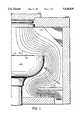
- FIG. 1shows various streamlines 5 of a downward and outward reactant gas flow within a CVD reaction space 7 which houses a substrate 8 which rotates on a rotating susceptor 6.
- the streamlines 5are from gas rings and a gas-dispersing showerhead (not shown) spaced approximately 4 inches or more above susceptor 6 and substrate 8.
- the streamlines 5illustrate what occurs when such a large spacing is used between the gas-dispensing rings and showerhead and the rotating substrate 8.
- the average size of the boundary layeris fairly significant and a substantial amount of the reactant gases 5 bypass rotating substrate 8 and pass around the baffle 11 to be exhausted out of the reaction space 7 by an appropriate exhaust system (not shown).
- the significant bypassing of the gases 5lowers the deposition rate because there is a reduced density of reactants available at the substrate surface 12 for the surface reaction.
- the wide boundary layer of reactant gases 5 at the substrate surface 11affects the uniformity of the film deposited on substrate 8. Still further, the wasted, unreacted gases which are exhausted make the overall deposition technique inefficient and costly.
- the inventionprovides apparatuses and methods for dispersing reactant gases close to a rotating substrate in a CVD reaction chamber such that there is improved reactant gas flow over the surface of the substrate and a reduced boundary layer for more efficient and uniform deposition and gas utilization. Further, the present invention produces a concentrated plasma at the rotating substrate to produce PECVD films particularly for PECVD of a titanium-containing film at low temperatures.
- the present inventionutilizes a gas-dispersing showerhead positioned within one inch of a rotating substrate.
- the showerheadis spaced a suitable distance below a gas-dispensing ring or other dispensing apparatus such that a steady state flow of gas develops between the ring and the showerhead before being disbursed by the showerhead over the rotating substrate.
- the showerheadis positioned within one inch of the substrate and preferably within 20 mm to produce a small gas boundary layer at the substrate for more efficient and more uniform deposition of a CVD film.
- a cylindrical structure or cylinderextends between a gas-dispensing ring which is coupled to a reactant gas supply and the showerhead.
- the reactant gasesare dispensed into the cylinder at one end spaced away from the substrate and flow down the length of the cylinder to be dispersed over the rotating substrate surface by the gas-dispersing holes in the showerhead.
- the velocity profile of the flow of incoming reactant gasesdevelops within the length of the cylinder and the cylinder confines the reactant gases such that preferably the reactant gases flow to the substrate surface only through the gas-dispersing showerhead.
- the close spacing of the showerhead, as well as the steady state flow of the gasesreduces the boundary layer over the substrate and ensures an efficient and uniform deposition of a CVD film on the substrate surface.
- the shape of the showerhead and the dimension of the gas-dispersing holeswhich are preferably 1/32 (0.0313) of an inch, flattens the velocity profile of the gases over the substrate to further produce a uniform gas flow to the substrate. Close spacing of the showerhead and the reduced boundary layer yields more efficient CVD with less of the reactant gases bypassing substrate.
- the showerheadis biased with RF energy to create an RF electrode for use in PECVD.
- Plasma gasespass through the RF showerhead/electrode and are excited proximate the showerhead/electrode to form a concentrated plasma close to the substrate which supplies energy to the surface reaction during PECVD (the showerhead will be referred to as a showerhead/electrode throughout the application where appropriate).
- the reduced spacing, i.e., less than 1 inch, between the showerhead/electrode and the substrate and the improved gas flow of the present inventionensure a concentrated plasma at the substrate surface which yields sufficient energy for the deposition of a film according to PECVD techniques.
- the showerhead/electrodeevenly disperses the reactant gases such that the concentrated plasma is uniform over the entire substrate surface.
- the cylinder and showerhead/electrode of the present inventionprevent ignition of a plasma above the showerhead/electrode and inside the cylinder, or even in the dispersing holes of the showerhead/electrode. In that way, the plasma is generally concentrated below the showerhead/electrode to enhance deposition and prevent contaminants within the plasma.
- the cylinderis made of nickel-plated aluminum and is coupled to a solid nickel showerhead/electrode by a quartz insulating ring.
- the insulating ringelectrically isolates the cylinder from the RF showerhead/electrode to prevent ignition of plasma in the cylinder.
- the entire cylinderis made out of an insulative quartz material to prevent formation of a plasma within the cylinder.
- the showerheadmay be approximately 0.25 inches thick and generally may have from 200 to 1,200 gas-dispersing holes depending upon the diameter of the showerhead and the substrates to be processed.
- the dispersing holes of the showerhead/electrodeare preferably 1/32 (0.0313) of an inch to further ensure that the plasma is confined below the showerhead/electrode.
- a preferred embodiment for processing six inch diameter substrate wafersemploys a circular showerhead with an approximately 6.5 inch diameter area having 300 to 600 gas dispersing holes.
- dimensions of the cylinder, showerhead and holesmay be adjusted depending upon, among other factors, the size of the chemical vapor deposition chamber, the desired showerhead distance from the substrate and the size of the substrate being processed.
- the cylinder and showerhead/electrode of the present inventionis operable to deliver approximately 200 to 300 watts of power at RF frequencies as low as 450 KHz and as high as 13.56 MHz. Additionally, the present invention operates sufficiently with reactant gas flow rates between 50 and 50,000 sccm, as well as susceptor rotation rates between 0 and 2,000 rpm.
- FIG. 1is a diagrammatic cross-sectional view of an example gas flow profile in a CVD reaction chamber with a rotating susceptor which does not utilize the present invention.
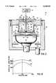
- FIG. 2is a cross-sectional view, of an embodiment of the present invention.
- FIG. 3is a diagrammatic cross-sectional view of an example gas flow profile in a CVD reaction chamber using the present invention.
- FIG. 4is a detailed view of the embodiment of the present invention illustrated in FIG. 2.
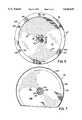
- FIG. 5is a top view of a gas-dispersing showerhead used with the embodiment of the present invention shown in FIGS. 2 and 4.
- FIG. 6is a cross-sectional view, of another embodiment of the present invention.
- FIG. 7is a top view of a gas-dispersing showerhead used with the embodiment of the present invention shown in FIG. 6.
- FIG. 8is a graphical illustration of the deposition ram versus rotation rate for a CVD reaction with and without the present invention.
- FIG. 2illustrates one embodiment of the present invention.
- a CVD reactor 20includes a deposition chamber housing 22 which defines a reaction or deposition space 24 therein.
- a rotating susceptor 26supports a substrate or wafer 28 within reaction space 24.
- a reactor suitable for the purposes of the present inventionis a Rotating Disk Reactor available from Materials Research Corporation (MRC) of Phoenix, Ariz.
- the reaction or deposition space 24 within housing 22may be selectively evacuated to various different internal pressures, for example, from 0.5 to 100 Torr.
- the susceptor 26is coupled to a variable speed motor (not shown) by shaft 30 such that the susceptor 26 and substrate 28 may be stationary or may be rotated at various speeds such as between 0 and 2,000 rpm. When rotating, susceptor 26 creates a downward pumping action in a direction generally perpendicular the substrate surface 29. Susceptor 26 is also heated by a suitable heating mechanism (not shown) coupled to the susceptor 26 so that susceptor 26 may heat substrate 28, such as between 200° and 800° C.
- a cylinder assembly 34Extending downwardly from the cover 32 of housing 22 is a cylinder assembly 34 which supports a gas-dispersing showerhead 36 above rotating susceptor 26 and substrate 28.
- the cylinder assembly 34preferably positions showerhead 36 within 1 inch of substrate 28 and more preferably within 20 mm of substrate 28.
- the cylinder assembly 34in combination with a generally circular opening 42 formed in the cover 32, forms a vertical flow passage which extends in the direction of reference arrows 43 between a gas distributor cover 46 and showerhead 36. Opening 42 of cover 32 forms a cylinder concentric with cylinder assembly 34 to define a generally cylindrical flow passage 44.
- showerhead 36may be coupled to an RF power source 38 such as by an appropriate RF feedline assembly 40 which extends through an opening 48 in the gas distributor cover 46.
- RF feedline assembly 40is used to bias showerhead 36 so that it acts as an electrode for PECVD techniques as explained in greater detail below.
- a sealing structure 49seals the opening 48 around feedline assembly 40.
- Plasma and reactant gasesare introduced into vertical flow passage 45 by concentric gas rings or halos 50, 52.
- other gas-dispensing structuresmight be utilized as are known by a person of ordinary skill in the art.
- the concentric rings 50, 52are coupled to appropriate gas supplies (not shown) through lines 56, 58, respectively and the rings include a number of gas-dispensing holes 54 which evenly dispense the gases around the perimeter of flow passage 44.
- showerhead 36includes gas-dispersing holes 64 for dispersing reactant gases over substrate 28.
- Cylinder assembly 34includes a cylinder 60 and an insulator ring 62 which electrically separates cylinder 60 and showerhead 36 whenever showerhead 36 is biased with RF energy.
- Cylinder 60is preferably electrically grounded by ground line 61.
- the insulator ring 62is preferably dimensioned in diameter and width as indicated by reference numeral 63 to ensure complete electrical separation between cylinder 60 and showerhead 36 along the entire attachment interface between the cylinder 60 and showerhead 36 (see FIG. 4).
- the insulator ringmay be made of quartz material such as Quartz T08-E available from General Electric and in one embodiment the ring has a thickness of approximately 0.75 inches.
- CVD reactant gasesare introduced at the top of flow passage 44 through rings 50, 52, and the gases are drawn generally downwardly in the direction of arrows 43 by the downward pumping action of rotating susceptor 26.
- the showerhead 36is preferably spaced from 2 to 4 inches from the rings 50, 52 to ensure a steady state flow of the gases at showerhead 36. More specifically, as the reactant gases flow downwardly through flow passage 44, a velocity profile develops. The velocity profile is a measurement of gas velocities at various points in the gas flow as measured across the gas flow perpendicular to the flow direction 43. Generally, the velocities across the gas flow at the top of the flow passage 44 near rings 50, 52 are generally equal.
- the velocity profile of the gas flowhas reached a steady state.
- the velocity of the reactant gas flowis generally greater in the center 67 of the showerhead 36 than it is at the periphery 69 of showerhead 36.
- showerhead 36flattens out the velocity profile of the reactant gas flow across the bottom surface 39 of the showerhead such that below showerhead 36 proximate substrate 28 the flow velocity near the center 67 of showerhead 36 is generally equal to the flow velocity at the periphery 69 of the showerhead 36.
- the spacing between the rings 50, 52 and showerhead 36 provided by cylinder assembly 34 and flow passage 44, and one inch or less spacing between showerhead 36 and rotating substrate 28 achieved by the present inventionyields uniform gas flow over the top surface 29 of substrate 28 with a very thin boundary layer.
- the streamlines of reactant gas flow 80are held much closer to the substrate 28.
- the boundary layer height as indicated by reference numeral 81is effectively reduced, and thus, there is a greater density of reactant gases present at the substrate surface 29 to take place in the chemical vapor deposition of a film. This ensures that a greater percentage of reactant gases are utilized in the CVD reaction, and therefore, a smaller percentage of the reactant gases bypass the substrate 28 unreacted to be exhausted by vacuum opening 71 around baffle 73 and out of the reaction space 24.
- the reactant gas flow through flow passage 44is drown downwardly and through showerhead 36 by the downward pumping action of the rotating susceptor 26.
- An increased susceptor rotation rateproduces an increased deposition rate because an increased quantity of reactants are being pumped to the surface. This is termed the rotating disk effect.
- the process curves in FIG. 8illustrate that the rotating disk effect occurs for the reduced showerhead-to-susceptor spacing achieved by the present invention. That is, as the rotation rate of the susceptor 26 increases, the deposition rate increases indicating that a greater quantity of reactants is being pumped to the surface 29 of substrate 28. A maximum deposition rate is reached whenever the incoming and downward gas flow to the substrate is equal to the outward flow of gas away from the substrate.
- matched gas flowSuch a condition is generally referred to as matched gas flow.
- the deposition rate curve for one embodiment of the present inventionshows higher deposition rates than the curve achieved without the present invention which is indicated by reference numeral 84.
- Curve 82indicates that less of the reactant gases are bypassing the wafer surface 29 in the present invention, and consequently, more are participating in the surface CVD reaction. Furthermore, curve 82 is flatter than curve 84 which indicates an improved process stability over a wider range of rotation rates when using the present invention
- the showerhead 36may be biased with RF energy to function as an RF electrode for PECVD techniques.
- plasma gasessuch as H 2 , N 2 and NH 3
- showerhead/electrode 36preferably below the showerhead/electrode 36 and not within cylinder 60.
- the approximate 1 inch or less spacing between the RF showerhead/electrode 36 and substrate 28creates a very concentrated plasma near substrate 28 which is useful for low temperature PECVD, and particularly for low temperature PECVD of titanium-containing films.
- RF power source 38biases showerhead/electrode 36.
- the electrically grounded susceptor 26forms another parallel electrode.
- An RF fieldis created preferably between showerhead 36 and susceptor 26 and the RF field excites the plasma gases which are dispersed through holes 64 so that a plasma is generated generally below showerhead/electrode 36. It is preferable that the plasma is created below the showerhead/electrode 36 and not within the flow space 44 above the showerhead/electrode 36. It is further preferable that the plasma is not created within dispersion holes 64 but rather is confined below the bottom surface 39 of showerhead/electrode 36.
- the dispersion holes 64are dimensioned so that the generated plasma is preferably confined below surface 39 of showerhead/electrode 36.
- the diameter of the dispersing holes 64is 1/32 of an inch.
- other features of the present inventionensure that the generated plasma is concentrated below the showerhead/electrode 36.
- insulator sleeves 96, 98are utilized within the RF feedline assembly 40 to insulate the RF line from the metal of cylinder 34 and housing 22 as illustrated in FIG. 4 and discussed in greater detail below.
- quartz insulator ring 62electrically separates the showerhead/electrode 36 from cylinder 34 to further confine the plasma below showerhead/electrode 36.
- the rotation of susceptor 26 and accompanying pumping action and the flow of gases within cylinder assembly 34 and flow passage 44ensures a uniform flow of gases to the plasma for uniformly sustained plasma and uniform deposition.
- a reactant gassuch as TiCl 4
- flow passage 44such as through a gas ring similar to rings 50 and 52, although the plasma gases and the reactant gases are preferably introduced through different rings.
- the gas particles of the reactant gasesare also excited by the RF field generated by showerhead/electrode 36 and susceptor 26 but do not form what would be defined as a plasma. Therefore, a mixture of excited reactant gas particles and a plasma of the plasma gas particles are concentrated above substrate 28 and preferably within 1 inch of the substrate in accordance with the principles of the present invention.
- the RF showerhead/electrode 36may be excited with RF energy having a frequency in the range of, for example, 450 KHz to 13.56 MHz, and the invention does not seem to be particularly frequency sensitive.
- the generation of a uniform plasma within 1 inch or less of substrate 28yields a high density of useful plasma gas radicals and ions proximate the substrate surface 29.
- the pumping action of the susceptordraws the plasma particles and excited reactant gas particles to the substrate to react and form a film.
- a substrate rotation ratesomewhere between 0 and 2,000 rpm might be utilized with the RF showerhead/electrode of the present invention.
- the showerhead/electrode 36 of the present inventiongenerates a plasma containing radicals and ions of the plasma gases
- the showerhead spacing and deposition parametersshould preferably be chosen to achieve a useful mixture of radicals and ions at the substrate surface 29. While some ion bombardment of the substrate 28 is beneficial because it supplies additional energy to the growing film layer on the surface 29, too much ion bombardment of a substrate may damage the integrated circuit devices on a substrate. Furthermore, a high density of ions leads to poor film conformality as ions have a tendency to stick to contact and via surfaces. As discussed above, showerhead/electrode-to-susceptor spacing within 1 inch and preferably within 20 mm has proven useful.
- FIG. 4discloses an RF showerhead/electrode configuration similar to the configuration in the embodiment of FIG. 2 except in greater detail. Wherever possible similar reference numerals will be utilized between FIGS. 2 and 4.
- the showerhead/electrode 36includes an RF line stem 68 mounted thereto which is one of several components making up the RF feedline assembly 40 supplying RF energy to showerhead/electrode 36.
- the RF feedline assembly 40also acts as a heat pipe to conduct heat away from showerhead/electrode 36 as is discussed in greater detail hereinbelow.
- Line stem 68may be machined concentrically into and integral with the upper surface 37 of showerhead/electrode 36 to increase the RF signal conduction and heat conduction efficiency see FIG. 5).
- the RF feedline assembly 40includes an RF line 92 which comprises line stem 68 and an additional length of tubing 94 welded thereto such as at 93 to achieve the desired overall length of the RF line 92 and to attach tubing 94 to the stem 68.
- the showerhead/electrode 36 and the integral line stem 68may be made of Nickel-200, while RF line tubing 94 may be made of a highly conductive material such as 6061-T6 aluminum.
- the RF line tubing 94is made of aluminum coated with an outer layer of nickel to prevent an RF plasma from forming within said cylinder 60 of the cylinder assembly 34 during use of the RF showerhead/electrode 36 according to the principles of the present invention.
- showerhead/electrode 36is perforated with a pattern of gas dispersion holes 64 to distribute the reactant and plasma gases evenly during CVD processing.
- upstanding RF line stem 68is provided with a circumferential shoulder flange 70 adjacent and extending generally parallel to showerhead/electrode 36.
- the flange 70is spaced above showerhead/electrode upper surface 37 and permits the gas dispersion hole pattern to extend beneath the shoulder flange 70, thereby minimizing gas flow disturbances.
- the flange 70aids in the conduction of the RF energy along line 92 to showerhead/electrode 36, assists in cooling showerhead/electrode 36, and provides mechanical support for ceramic isolator tubes 96, 98.
- the RF showerhead/electrode assembly 34 of FIG. 4further includes first and second ceramic isolator tubes 96, 98, respectively, which are concentric with and surround at least a portion of RF line 92.
- ceramic isolator tubes 96, 98are supported by circumferential shoulder flange 70.
- Tubes 96, 98may be formed of the ceramic alumina (99.7% Al 2 O 3 ), which is readily commercially available, such as from Coors Ceramics of Golden, Colo.
- Isolator tubes 96, 98prevent RF plasma from forming around the RF line 92 during CVD processing by isolating the metal RF line 92 from any of the plasma and reactant gases present within the cylinder 60.
- the isolator tubes 96, 98operate to reduce and prevent electrical shorting between gas distributor cover 100 (which is at ground potential) and RF line 92 at the opening 48 where RF line 92 passes through gas distributor cover 100.
- Gas distributor cover 100is mounted to housing 22 by means of a plurality of screws 102.
- gas injection rings or halossuch as rings 50, 52 (shown in phantom in FIG. 4) are located slightly below gas distributor cover 100 to supply the CVD reactant and plasma gases to the inside of cylinder 60 as already discussed.
- Gas injection rings 50, 52may be only two of a plurality of concentric rings for introducing numerous reactant gases into the cylinder 60.
- a seal assembly 49prevents vacuum leaks at the opening 48 where RF line 92 passes through gas distributor cover 100.
- This assemblyincludes a shaft seal and a flange seal.
- a ceramic seal plate 104is pressed downwardly by two stainless steel clamps 106.
- Clamps 106are biased against distributor cover 100 by spring washer/screw assemblies 108 to obtain a predetermined downward force on the seal components to insure proper sealing, to accommodate tolerance stacks in the seal components, and to take up dimensional changes due to thermal expansion which may occur during CVD processing.
- Seal plate 104presses downwardly on a stainless steel ferrule 110 which in turn presses down on an O-ring 112 seated in ceramic seal body 114.
- the downward force exerted by clamps 106 on seal plate 104also forces seal body 114 downwardly against gas distributor cover 100, which compresses the O-ring 116 located between seal body 114 and gas distributor cover 100.
- seal body 114has a downwardly extending annular flange 118 which surrounds RF line 92 over the entire length of it which passes through gas distributor cover 100.
- the lower end 120 of annular flange 118extends downwardly to a point where it meets the inner ceramic isolator tube 96.
- the outer ceramic isolator tube 98extends further upward than isolator tube 96, such that there is no direct line between gas distributor cover 100 and RF line 92. This prevents arcing when the RF line 92 is used to supply RF energy to showerhead/electrode 36.
- the RF line 92also functions as a heat pipe structure.
- the heat pipe structureis used to carry off heat from the showerhead/electrode 36 generated by radiant energy from the heated susceptor 26, as well as by the RF energy applied to the showerhead/electrode 36.
- the center space 122 of RF line 92is provided with a felt or other suitable capillary wicking material liner (not shown).
- Space 122is sealed with a liquid (e.g., acetone) therein under its own vapor pressure that enters the pores of the capillary material wetting all internal surfaces of RF line 92.
- a liquide.g., acetone
- the liquid at that pointboils and enters a vapor state.
- the liquid in the wicking materialpicks up the latent heat of vaporization and the vapor, which then is at a higher pressure, moves inside the sealed pipe to a cooler location where it condenses and re-enters the liner.
- the vaporgives up its latent heat of vaporization and moves heat from the "input" to the "output" end of the heat pipe structure.
- heatmay be moved along a heat pipe at a rate of approximately 500 mph.
- the "input" end of the heat pipe structureis the end of RF line 92 which is affixed to showerhead/electrode 36.
- the “output” endis the upper end of RF line 92 shown in the FIG. 4 which has a liquid-cooling jacket 124 sealed around it. The seal is effected by O-ring shaft seals 125 and 126.
- Cooling jacket 124is preferably a polymeric material and is provided with TEFLON compression fittings 128 and 129 which connect TEFLON tubing 130 to cooling jacket 124.
- RF line 92also includes a cap 132 which is welded in place and has a fill tube 134 for filling the internal space 122 with the desired fluid.
- a suitable commercially available heat pipemay be obtained from Thermocore Inc., of Lancaster, Pa.
- cylinder 60forms part of cylinder assembly 34 and mounts showerhead/electrode 36 to the housing cover 32.
- the cylinder 60is dimensioned such that the showerhead/electrode 36 is positioned generally within 1 inch of susceptor 26 after taking into account the thickness of ring 62.
- Showerhead/electrode 36is fastened to cylinder 60 by means of screws 136, which are preferably made of a material that does not corrode in the presence of an RF plasma.
- screws 136are preferably made of a material that does not corrode in the presence of an RF plasma.
- Hastelloy C-22which is a trade name of Hanes International, of Kokomo, Ind. Suitable screws made of this material are available from Pinnacle Mfg. of Tempe, Ariz.
- Insulator ring 62electrically isolates showerhead/electrode 36 from cylinder 60.
- the insulator ringmay be formed of quartz and preferably of a suitable quality quartz which has few and/or very small internal blemishes such as air bubbles.
- a suitable quartz materialis Quartz T08-E available from Hereaus Amersil of Tempe, Ariz. The quartz may be machined to form a quartz ring approximately 3/4 (0.75) inches thick and having diameter dimensions which match the dimensions of the cylinder 60 and showerhead/electrode 36 between which the insulator ring 62 is fixed. Screws 136, which are at ground potential, are isolated from the showerhead/electrode 36 by two interlocking ceramic isolator sleeves 138 and 139.
- Quartz ring 62while insulating showerhead/electrode 36 from cylinder 60, is also used because of the significant resistance of quartz to thermal shock. This is important because the RF showerhead/electrode 36 below ring 62 becomes heated to a higher temperature, and more rapidly, than cylinder 60 above quartz ring 62, thus inducing thermal shock and stress in ring 62.
- Screws 140which may be made of the same material as screws 136, are utilized to affix cylinder 60 to housing 22.
- RF energyis conducted to showerhead/electrode 36 by RF feedline assembly 40 comprising stem 68 and tube 94.
- Isolator tubes 96, 98are needed to electrically isolate and prevent arcing between tube 94 and any parts of the metal housing 22, including distributor cover 100.
- the apparatusincludes a seal around tubing 94 at the location where it passes through distributor cover 100.
- RF energyis supplied through a shielded RF supplying cable 142 which is connected to an RF power source 38 (shown in FIG. 2) and has a UHF connector 144 at one end. Connector 144 mates with another UHF connector 146, which in turn is coupled via a length of 12 gauge wire 148 to a stainless steel shaft collar 150 mounted at the upper end of RF line 92.
- the shaft collar 150is in frictional contact with RF line 92.
- collar 150may include opposing clam-shell clamps which may be tightened against one another by means not shown to firmly grip line 92. With this arrangement there is minimal resistance to the flow of RF current through line 92.
- the segment of RF line 92 which is exposed above shaft collar 150is isolated from the grounded metal shielding 152 by a polymer cap 154.
- the apparatusis capable of delivering 250-300 watts of RF frequencies from 450 KHz to 13.56 MHz.
- FIG. 5discloses a top flew, of one showerhead design appropriate for the embodiment of the present invention shown in FIGS. 2 and 4.
- showerhead 36is generally circular and includes dispersion holes 64 generally throughout its entire area.
- showerhead 36may be approximately 8.0 inches in total diameter with an area 156 containing holes 64 having a diameter of 6.5 inches.
- the diameter of the showerhead 36 and the hole area 156will depend upon the size of the substrate wafers which are processed using the current invention.
- showerhead 36may have generally from 200 to 1,200 dispersion holes 64 and preferably for an 8.0 inch showerhead has from 300 to 600 holes for dispersing the gases.
- the inner diameter of the holes 64is preferably 1/32 (0.0313) inches, to prevent a plasma from forming within the cylinder 60.
- showerhead 36includes a peripheral edge section 157 with spaced openings 158 spaced around the periphery of showerhead 36 which receive screws 136 or other fasteners for connecting showerhead 36 to the quartz ring as shown in FIG. 4.
- the showerhead 36includes a stem 68 which forms flange 70.
- Stem 68 and flange 70are formed integrally with showerhead 36 and form part of the RF line assembly 40 connected to showerhead 36.
- the showerhead, 36, including stem 68is formed of an electrically conductive material and preferably is formed of Nickel-200.
- the showerhead 36 in one embodiment of the inventionhas a thickness dimension in the holed area 156 of preferably 1/4 (0.25) inches.
- FIGS. 2 and 4have been utilized to deposit layers of titanium and titanium nitride at low substrate temperatures.
- Various examples of CVD and PECVD methods and use of the present inventionare illustrated below. Deposition parameters are given for each example and the results of the deposition are illustrated in tables associated with particular parameters.
- Table 1illustrates use of the apparatuses of the present invention to deposit a titanium nitride (TIN) layer on a substrate utilizing both nitrogen gas (N 2 ) and hydrogen gas (H 2 ) and titanium tetrachloride (TiCl 4 ).
- Wafers 1 and 2 of Table 1were silicon, while the remaining wafers 3-10 were thermal oxide.
- Wafers 6-10received a 250 Watt RF plasma anneal for 120 seconds at an NH 3 gas rate of 5000 sccm, at an internal pressure of 3 Torr (wafer 6 was done at 5 Torr), and the susceptor rotation rate of 100 rpm. Therefore, as may be seen, a layer of titanium nitride may be deposited at a substrate temperature approximately 400° C., which is substantially less than the temperatures required for traditional thermal CVD processes.
- Table 2The example of Table 2 below was accomplished with the parameters of Table 1 except at a substrate temperature of 600° C., and a layer of TiN was deposited according to Table 2 using the deposition parameters below.
- Wafers 1 and 2 of Table 2were silicon and wafers 3-8 were thermal oxide.
- An RF plasma, ammonia annealwas performed on substrate wafers 6-8 of Table 2 at a power lever of 250 Watts for 120 seconds, and an ammonia introduction rate of 5000 sccm, a pressure of 5 Torr and a 100 rpm rotation rate.
- FIGS. 2 and 4have also been utilized to deposit a layer of pure titanium.
- Table 3sets forth the results and parameters of a deposition run which resulted in a deposited film of approximately 84% titanium on a thermal oxide wafer at 650° C. This was an excellent result for such low temperature chemical vapor deposition.
- the substrate wafer of Table 3was not annealed with an ammonia plasma as discussed above.
- Table 5shows additional runs made with the increased H 2 flow and increase deposition pressure.
- Deposition time (sec) 300(wafers 9-12 600 seconds)
- the change in deposition pressure from 1 Torr to 5 Torrproduced a more stable and symmetric plasma. Additionally, the increased hydrogen flow with the addition of a small flow of argon increased the stability of the plasma flow as well as the plasma intensity. An argon flow of 0-10 slm is preferable.
- Wafers 1-2were silicon, while wafers 3-10 were thermal oxide.
- Wafers 11 and 12were borophospho-silicate glass, available from Thin Films, Inc. of Freemont, Calif. None of the wafers of either Table 4 or 5 were annealed with an ammonia plasma anneal.
- Table 6shows additional deposition runs at a susceptor temperature of 450° C.
- Substrate Temperatureapproximately 400° C.
- Wafers 1-4were silicon, wafer 5 was thermal oxide, while wafers 6 and 7 were aluminum alloy containing aluminum silicon and copper.
- Runs 6 and 7 of Table 6illustrate the viability of depositing a titanium-containing film on aluminum using the present invention.
- the deposition runs of Table 6utilized a lower flow of reactant gas than the runs of Table 5, i.e., 5 sccm of TiCl 4 .
- Deposition time (sec) 300wafers 1 and 2 at 180 and 240, respectively.
- Substrate Temperatureapproximately 400° C.
- FIG. 6shows an alternative embodiment of the present invention which eliminates the metal cylinder 60 and insulator ring 62 while preventing electrical arcing inside of the cylinder assembly proximate the RF line and preventing the undesired formation of plasma within the cylinder assembly when the showerhead is biased as an electrode.
- the embodiment of FIG. 6utilizes a housing similar to housing 22 of FIG. 4 which includes a housing cover 160 and includes an RF supply assembly 162, a heat pipe assembly 164 with cooling jacket 165 and fluid supply lines and a gas distributor cover 166 with a sealing assembly 168 all generally similar to the respective components of FIG. 4.
- the cylinder assembly 170does not include a metal cylinder 60 and insulator ring 62. Rather, a cylinder 172 made of insulating material such as quartz surrounds the RF feed line assembly 174.
- Cylinder 172is preferably formulated out of a high quality quartz such as Quartz T08-E available from Hereaus Amersil, as mentioned above. Quartz cylinder 172 is supported by a showerhead/electrode 176, made of a conductive metal such as Nickel-200, without the use of screws or other fasteners that are utilized within the embodiment of FIG. 4. Specifically, a stepped bore 178 is formed within housing cover 160 to receive an upper end 177 of cylinder 172. O-rings 179, 180 are placed at the interface 181 between stepped bore 178 and cylinder 172 to form a seal at interface 181.
- a stepped bore 178is formed within housing cover 160 to receive an upper end 177 of cylinder 172. O-rings 179, 180 are placed at the interface 181 between stepped bore 178 and cylinder 172 to form a seal at interface 181.
- an annular notch 186is formed in cylinder 172 to receive a peripheral edge 188 of the showerhead/electrode 176.
- the notch 186 of cylinder 172rests upon the peripheral edge 188 of showerhead/electrode 176.
- showerhead/electrode 176includes a stem 194 which is attached to RF line tubing 175 such as by a weld at 195 to form a unitary RF line 197.
- RF lineis frictionally held and supported at its top end by collar 199 similar to collar 150 of FIG. 4.
- the RF linesupports showerhead/electrode 176 above susceptor 182.
- showerhead/electrode 176supports the cylinder 172 within the cylinder assembly 170 by abutting against cylinder 172 at shelf notch and holding it in bore 178.
- the interface between showerhead/electrode peripheral edge 188 and cylinder notch 186is sealed by a compressed O-ring 190 which is compressed between notch 186 and a corresponding annular notch 193 formed in peripheral edge 188.
- a plurality of gas halos or rings 191,192introduce the necessary plasma and reactant gases into cylinder 172.
- FIG. 6eliminates the need for metal screws to attach the cylinder 172 to the housing 160 and the showerhead/electrode 176 to the cylinder 172. This further reduces the possibility of arcing inside of cylinder 172 because of the reduced metal proximate the biased RF showerhead/electrode 176. Furthermore, it is not necessary to utilize ceramic isolator sleeves at the showerhead peripheral edge 188.
- showerhead/electrode 176has also been modified.
- showerhead/electrodeincludes a stem 194 without a flange. Instead, a slight ridge 196 is formed around stem 194, and as shown in FIG. 6, ridge 196 supports a generally circular ceramic tray 198 which is formed from a ceramic material similar to the ceramic isolator sleeves 94, 96 shown in FIG. 4. Ceramic tray 198 is supported by ridge 194, and in turn, supports isolator sleeves 200, 201.
- Isolator sleeves 200, 201are also preferably made of a ceramic insulator material similar to sleeves 94, 96 of FIG. 4.
- gas dispersion holes 206are formed within an area 204 similar to the dispersion hole area 156 of the showerhead/electrode shown in FIG. 4. Preferably the holes are approximately 1/32 (0.0313) inches in diameter to prevent the formation of a plasma inside cylinder 172 to confine the plasma generally below the showerhead/electrode 176 and above the susceptor 182 as already discussed above.
- FIG. 4The embodiment of FIG.
- a layer of insulation 208may be placed atop gas distributor cover 166 to prevent contact by an operator, because the gas distributor cover 166 becomes very hot during operation.
Landscapes
- Chemical & Material Sciences (AREA)
- Engineering & Computer Science (AREA)
- Metallurgy (AREA)
- Chemical Kinetics & Catalysis (AREA)
- Materials Engineering (AREA)
- Mechanical Engineering (AREA)
- General Chemical & Material Sciences (AREA)
- Organic Chemistry (AREA)
- Physics & Mathematics (AREA)
- Plasma & Fusion (AREA)
- Fluid Mechanics (AREA)
- Chemical Vapour Deposition (AREA)
- Electrodes Of Semiconductors (AREA)
Abstract
Description
TABLE NO. 1 __________________________________________________________________________Results and Additional WAFER NO. Parameters 1 2 3 4 5 6 7 8 9 10 __________________________________________________________________________TiN layer 825 1023 1221 1262 1227 1224 1141 1348 1400 1106 thickness (Å) Deposition 275 341 407 421 409 408 380 449 487 389 Rate (Å/min) Layer 1530 2686 4118 3108 855 4478 3982 4658 3449 4501 Resistivity 4 cm)u.Ω Susceptor 470 480 488 470 470 460 460 460 460 460 Temp (°C.) __________________________________________________________________________
TABLE NO. 2 ______________________________________ Results and Additional WAFER NO. Parameters 1 2 3 4 5 6 7 8 ______________________________________ TiN layer 657 822 740 768 767 765 773 910 thickness (Å) Deposition 219 274 247 263 256 255 258 303 Rate (Å/min) Layer 391 254 432 543 471 949 973 2710 Resistivity cm)u.Ω Susceptor 650 650 650 650 650 650 650 650 Temp (°C.) ______________________________________
TABLE NO. 3 ______________________________________ Results and Additional WAFER NO. Parameters 1 ______________________________________ Ti layer 1983 thickness (Å)Deposition 44 Rate (Å/min) Layer 929 Resistivity cm)u.Ω Susceptor 651 Temp (°C.) ______________________________________
TABLE 4 __________________________________________________________________________Results and Additional WAFER NO. Parameters 1 2 3 4 5 6 7 8 9 __________________________________________________________________________TiN layer 798 1076 43.4 89.5 912.2 1082 656.5 577.1 1302 thickness (Å) Deposition 159.0 215.0 9.1 17.9 182.5 216.5 131.3 115.4 130.2 Rate (Å/min) Layer 53.84 32.66 216.1 377.1 89.23 25.7 212.7 211.3 170.1 Resistivity cm)u.Ω __________________________________________________________________________
TABLE NO. 5 __________________________________________________________________________Results and Additional WAFER NO. Parameters 1 2 3 4 5 6 7 8 9 10 11 12 __________________________________________________________________________TiN layer 889.6 3994 510.3 458.6 466.2 385.6 347.8 263.3 792.5 948.8 749.7 714.4 thickness (Å) Deposition 177.9 79.9 102.1 91.7 93.2 77.1 69.6 52.7 79.3 94.9 75.0 71.4 Rate (Å/min) Layer 54.03 35.71 233.4 274.1 281.0 280.1 545.1 489.1 314.1 203.5 -- -- Resistivity (μΩ-cm) __________________________________________________________________________
TABLE NO. 6 ______________________________________ Results and Additional WAFER NO. Parameters 1 2 3 4 5 6 7 ______________________________________ TiN layer 242 222 210 241 168 136 150 thickness (Å) Deposition 80.7 74.0 70.0 80.3 56.0 45.3 50.0 Rate (Å/min) Layer 66.0 554.0 494.0 714.0 484.0 0.1 0.1 Resistivity cm)u.Ω ______________________________________
TABLE NO. 7 ______________________________________ Results and Additional WAFER NO. Parameters 1 2 3 4 5 6 7 ______________________________________ TiN layer 89 132 158 149 158 166 107 Thickness (Å) Deposition 30 33 32 32 32 33 21 Rate (Å/min) Layer 259 239 199 199 190 209 482 Resistivity cm)u.Ω ______________________________________
Claims (20)
Priority Applications (10)
| Application Number | Priority Date | Filing Date | Title |
|---|---|---|---|
| US08/253,714US5628829A (en) | 1994-06-03 | 1994-06-03 | Method and apparatus for low temperature deposition of CVD and PECVD films |
| JP8500804AJPH10501300A (en) | 1994-06-03 | 1994-11-29 | Low-temperature film forming method and apparatus by CVD method and PECVD method |
| KR1019960706959AKR970703446A (en) | 1994-06-03 | 1994-11-29 | Method and apparatus for low temperature deposition of CVD and PECVD films |
| DE69414274TDE69414274T2 (en) | 1994-06-03 | 1994-11-29 | METHOD AND DEVICE FOR THE LOW-TEMPERATURE DEPOSIT OF CVD AND PECVD FILMS |
| CA002191456ACA2191456A1 (en) | 1994-06-03 | 1994-11-29 | Method and apparatus for low temperature deposition of cvd and pecvd films |
| PCT/US1994/013614WO1995033868A1 (en) | 1994-06-03 | 1994-11-29 | Method and apparatus for low temperature deposition of cvd and pecvd films |
| EP95904143AEP0763149B1 (en) | 1994-06-03 | 1994-11-29 | Method and apparatus for low temperature deposition of cvd and pecvd films |
| AU12947/95AAU1294795A (en) | 1994-06-03 | 1994-11-29 | Method and apparatus for low temperature deposition of cvd and pecvd films |
| TW084100024ATW335593B (en) | 1994-06-03 | 1995-01-05 | Method and apparatus for low temperature deposition of CVD and PECVD films |
| US08/615,453US6140215A (en) | 1994-06-03 | 1996-03-14 | Method and apparatus for low temperature deposition of CVD and PECVD films |
Applications Claiming Priority (1)
| Application Number | Priority Date | Filing Date | Title |
|---|---|---|---|
| US08/253,714US5628829A (en) | 1994-06-03 | 1994-06-03 | Method and apparatus for low temperature deposition of CVD and PECVD films |
Related Child Applications (1)
| Application Number | Title | Priority Date | Filing Date |
|---|---|---|---|
| US08/615,453DivisionUS6140215A (en) | 1994-06-03 | 1996-03-14 | Method and apparatus for low temperature deposition of CVD and PECVD films |
Publications (1)
| Publication Number | Publication Date |
|---|---|
| US5628829Atrue US5628829A (en) | 1997-05-13 |
Family
ID=22961417
Family Applications (2)
| Application Number | Title | Priority Date | Filing Date |
|---|---|---|---|
| US08/253,714Expired - LifetimeUS5628829A (en) | 1994-06-03 | 1994-06-03 | Method and apparatus for low temperature deposition of CVD and PECVD films |
| US08/615,453Expired - LifetimeUS6140215A (en) | 1994-06-03 | 1996-03-14 | Method and apparatus for low temperature deposition of CVD and PECVD films |
Family Applications After (1)
| Application Number | Title | Priority Date | Filing Date |
|---|---|---|---|
| US08/615,453Expired - LifetimeUS6140215A (en) | 1994-06-03 | 1996-03-14 | Method and apparatus for low temperature deposition of CVD and PECVD films |
Country Status (9)
| Country | Link |
|---|---|
| US (2) | US5628829A (en) |
| EP (1) | EP0763149B1 (en) |
| JP (1) | JPH10501300A (en) |
| KR (1) | KR970703446A (en) |
| AU (1) | AU1294795A (en) |
| CA (1) | CA2191456A1 (en) |
| DE (1) | DE69414274T2 (en) |
| TW (1) | TW335593B (en) |
| WO (1) | WO1995033868A1 (en) |
Cited By (187)
| Publication number | Priority date | Publication date | Assignee | Title |
|---|---|---|---|---|
| US5853484A (en)* | 1995-10-28 | 1998-12-29 | Lg Semicon Co., Ltd. | Gas distribution system and method for chemical vapor deposition apparatus |
| WO1999023698A1 (en)* | 1997-11-05 | 1999-05-14 | Tokyo Electron Limited | Titanium nitride contact plug formation |
| US5926737A (en)* | 1997-08-19 | 1999-07-20 | Tokyo Electron Limited | Use of TiCl4 etchback process during integrated CVD-Ti/TiN wafer processing |
| US5997649A (en)* | 1998-04-09 | 1999-12-07 | Tokyo Electron Limited | Stacked showerhead assembly for delivering gases and RF power to a reaction chamber |
| US6050506A (en)* | 1998-02-13 | 2000-04-18 | Applied Materials, Inc. | Pattern of apertures in a showerhead for chemical vapor deposition |
| US6069093A (en)* | 1997-06-25 | 2000-05-30 | Tokyo Electron Limited | Process of forming metal films and multi layer structure |
| US6079356A (en)* | 1997-12-02 | 2000-06-27 | Applied Materials, Inc. | Reactor optimized for chemical vapor deposition of titanium |
| US6087261A (en)* | 1997-09-30 | 2000-07-11 | Fujitsu Limited | Method for production of semiconductor device |
| US6090705A (en)* | 1998-01-20 | 2000-07-18 | Tokyo Electron Limited | Method of eliminating edge effect in chemical vapor deposition of a metal |
| US6106625A (en)* | 1997-12-02 | 2000-08-22 | Applied Materials, Inc. | Reactor useful for chemical vapor deposition of titanium nitride |
| US6121140A (en)* | 1997-10-09 | 2000-09-19 | Tokyo Electron Limited | Method of improving surface morphology and reducing resistivity of chemical vapor deposition-metal films |
| US6161500A (en)* | 1997-09-30 | 2000-12-19 | Tokyo Electron Limited | Apparatus and method for preventing the premature mixture of reactant gases in CVD and PECVD reactions |
| US6182603B1 (en)* | 1998-07-13 | 2001-02-06 | Applied Komatsu Technology, Inc. | Surface-treated shower head for use in a substrate processing chamber |
| US6184158B1 (en)* | 1996-12-23 | 2001-02-06 | Lam Research Corporation | Inductively coupled plasma CVD |
| US6220202B1 (en) | 1994-06-03 | 2001-04-24 | Tokyo Electron Limited | Apparatus for producing thin films by low temperature plasma-enhanced chemical vapor deposition |
| US6284668B1 (en)* | 1995-08-10 | 2001-09-04 | Tokyo Electron Limited | Plasma polishing method |
| US6289842B1 (en) | 1998-06-22 | 2001-09-18 | Structured Materials Industries Inc. | Plasma enhanced chemical vapor deposition system |
| US6302057B1 (en) | 1998-09-15 | 2001-10-16 | Tokyo Electron Limited | Apparatus and method for electrically isolating an electrode in a PECVD process chamber |
| US6402848B1 (en)* | 1999-04-23 | 2002-06-11 | Tokyo Electron Limited | Single-substrate-treating apparatus for semiconductor processing system |
| US20020069968A1 (en)* | 2000-01-20 | 2002-06-13 | Ernst Keller | Suspended gas distribution manifold for plasma chamber |
| US6440494B1 (en) | 2000-04-05 | 2002-08-27 | Tokyo Electron Limited | In-situ source synthesis for metal CVD |
| US20020152960A1 (en)* | 2000-06-23 | 2002-10-24 | Masahiko Tanaka | Thin-film disposition apparatus |
| US6499425B1 (en) | 1999-01-22 | 2002-12-31 | Micron Technology, Inc. | Quasi-remote plasma processing method and apparatus |
| US6534423B1 (en)* | 2000-12-27 | 2003-03-18 | Novellus Systems, Inc. | Use of inductively-coupled plasma in plasma-enhanced chemical vapor deposition reactor to improve film-to-wall adhesion following in-situ plasma clean |
| US6642662B2 (en)* | 2001-11-02 | 2003-11-04 | Jusung Engineering Co. Ltd. | Plasma apparatus |
| US20040118345A1 (en)* | 2000-01-20 | 2004-06-24 | Applied Materials, Inc. | Flexibly suspended gas distribution manifold for plasma chamber |
| US20040250766A1 (en)* | 2003-04-30 | 2004-12-16 | Tokyo Electron Limited | Hybrid ball-lock attachment apparatus |
| US20050056217A1 (en)* | 2003-08-06 | 2005-03-17 | Takakazu Yamada | Shower head, device and method for manufacturing thin films |
| US20050081788A1 (en)* | 2002-03-15 | 2005-04-21 | Holger Jurgensen | Device for depositing thin layers on a substrate |
| US20050183827A1 (en)* | 2004-02-24 | 2005-08-25 | Applied Materials, Inc. | Showerhead mounting to accommodate thermal expansion |
| US20050251990A1 (en)* | 2004-05-12 | 2005-11-17 | Applied Materials, Inc. | Plasma uniformity control by gas diffuser hole design |
| US20060021703A1 (en)* | 2004-07-29 | 2006-02-02 | Applied Materials, Inc. | Dual gas faceplate for a showerhead in a semiconductor wafer processing system |
| US20060060138A1 (en)* | 2004-09-20 | 2006-03-23 | Applied Materials, Inc. | Diffuser gravity support |
| US20060086439A1 (en)* | 2003-06-25 | 2006-04-27 | United Technologies Corporation | Clean atmosphere heat treat for coated turbine components |
| US20060228496A1 (en)* | 2004-05-12 | 2006-10-12 | Applied Materials, Inc. | Plasma uniformity control by gas diffuser curvature |
| US20070044714A1 (en)* | 2005-08-31 | 2007-03-01 | Applied Materials, Inc. | Method and apparatus for maintaining a cross sectional shape of a diffuser during processing |
| US20070137574A1 (en)* | 2005-12-21 | 2007-06-21 | Porponth Sichanugrist | Low-cost and high performance solar cell manufacturing machine |
| US20080020146A1 (en)* | 2004-05-12 | 2008-01-24 | Choi Soo Y | Diffuser plate with slit valve compensation |
| US20080099146A1 (en)* | 2006-10-25 | 2008-05-01 | Applied Materials, Inc. | Suspension for showerhead in process chamber |
| US20080099145A1 (en)* | 2005-09-02 | 2008-05-01 | Applied Materials, Inc. | Gas sealing skirt for suspended showerhead in process chamber |
| US20080317973A1 (en)* | 2007-06-22 | 2008-12-25 | White John M | Diffuser support |
| US7543547B1 (en)* | 2002-07-31 | 2009-06-09 | Lam Research Corporation | Electrode assembly for plasma processing apparatus |
| US20100075509A1 (en)* | 2008-09-22 | 2010-03-25 | Hironobu Hirata | Manufacturing method and manufacturing apparatus for semiconductor device |
| US20100166957A1 (en)* | 2003-08-07 | 2010-07-01 | Sundew Technologies, Llc | Perimeter partition-valve with protected seals and associated small size process chambers and multiple chamber systems |
| US20100224130A1 (en)* | 2005-06-08 | 2010-09-09 | Jacob Smith | Rotating substrate support and methods of use |
| US20100267191A1 (en)* | 2009-04-20 | 2010-10-21 | Applied Materials, Inc. | Plasma enhanced thermal evaporator |
| US20110215071A1 (en)* | 2010-03-03 | 2011-09-08 | Veeco Instruments Inc. | Wafer carrier with sloped edge |
| TWI424515B (en)* | 2007-02-06 | 2014-01-21 | Sosul Co Ltd | Apparatus for forming a layer |
| US20140076234A1 (en)* | 2004-02-26 | 2014-03-20 | Applied Materials, Inc. | Multi chamber processing system |
| US20140099794A1 (en)* | 2012-09-21 | 2014-04-10 | Applied Materials, Inc. | Radical chemistry modulation and control using multiple flow pathways |
| US8778079B2 (en) | 2007-10-11 | 2014-07-15 | Valence Process Equipment, Inc. | Chemical vapor deposition reactor |
| US20140238608A1 (en)* | 2013-02-28 | 2014-08-28 | Novellus Systems, Inc. | Ceramic showerhead with embedded rf electrode for capacitively coupled plasma reactor |
| US20150079807A1 (en)* | 2013-09-13 | 2015-03-19 | Tokyo Electron Limited | Method of manufacturing a silicon oxide film |
| WO2015094596A1 (en)* | 2013-12-17 | 2015-06-25 | Applied Materials, Inc. | Semiconductor system assemblies and methods of operation |
| US20150279672A1 (en)* | 2012-10-26 | 2015-10-01 | Aledia | Process for growing at least one nanowire using a transition metal nitride layer obtained in two steps |
| US20150284841A1 (en)* | 2012-12-20 | 2015-10-08 | Stefan Keller | Plasma enhanced deposition arrangement for evaporation of dielectric materials, deposition apparatus and methods of operating thereof |
| US9269590B2 (en) | 2014-04-07 | 2016-02-23 | Applied Materials, Inc. | Spacer formation |
| US9287134B2 (en) | 2014-01-17 | 2016-03-15 | Applied Materials, Inc. | Titanium oxide etch |
| US9287095B2 (en) | 2013-12-17 | 2016-03-15 | Applied Materials, Inc. | Semiconductor system assemblies and methods of operation |
| US9293568B2 (en) | 2014-01-27 | 2016-03-22 | Applied Materials, Inc. | Method of fin patterning |
| US9299538B2 (en) | 2014-03-20 | 2016-03-29 | Applied Materials, Inc. | Radial waveguide systems and methods for post-match control of microwaves |
| US9299537B2 (en) | 2014-03-20 | 2016-03-29 | Applied Materials, Inc. | Radial waveguide systems and methods for post-match control of microwaves |
| US9299583B1 (en) | 2014-12-05 | 2016-03-29 | Applied Materials, Inc. | Aluminum oxide selective etch |
| US9299575B2 (en) | 2014-03-17 | 2016-03-29 | Applied Materials, Inc. | Gas-phase tungsten etch |
| US9309598B2 (en) | 2014-05-28 | 2016-04-12 | Applied Materials, Inc. | Oxide and metal removal |
| US9324576B2 (en) | 2010-05-27 | 2016-04-26 | Applied Materials, Inc. | Selective etch for silicon films |
| US9343272B1 (en) | 2015-01-08 | 2016-05-17 | Applied Materials, Inc. | Self-aligned process |
| US9349605B1 (en) | 2015-08-07 | 2016-05-24 | Applied Materials, Inc. | Oxide etch selectivity systems and methods |
| US9355856B2 (en) | 2014-09-12 | 2016-05-31 | Applied Materials, Inc. | V trench dry etch |
| US9355862B2 (en) | 2014-09-24 | 2016-05-31 | Applied Materials, Inc. | Fluorine-based hardmask removal |
| US9355863B2 (en) | 2012-12-18 | 2016-05-31 | Applied Materials, Inc. | Non-local plasma oxide etch |
| US9368364B2 (en) | 2014-09-24 | 2016-06-14 | Applied Materials, Inc. | Silicon etch process with tunable selectivity to SiO2 and other materials |
| US9373522B1 (en) | 2015-01-22 | 2016-06-21 | Applied Mateials, Inc. | Titanium nitride removal |
| US9373517B2 (en) | 2012-08-02 | 2016-06-21 | Applied Materials, Inc. | Semiconductor processing with DC assisted RF power for improved control |
| US9378978B2 (en) | 2014-07-31 | 2016-06-28 | Applied Materials, Inc. | Integrated oxide recess and floating gate fin trimming |
| US9378969B2 (en) | 2014-06-19 | 2016-06-28 | Applied Materials, Inc. | Low temperature gas-phase carbon removal |
| US9384997B2 (en) | 2012-11-20 | 2016-07-05 | Applied Materials, Inc. | Dry-etch selectivity |
| US9385028B2 (en) | 2014-02-03 | 2016-07-05 | Applied Materials, Inc. | Air gap process |
| US9390937B2 (en) | 2012-09-20 | 2016-07-12 | Applied Materials, Inc. | Silicon-carbon-nitride selective etch |
| US9396989B2 (en) | 2014-01-27 | 2016-07-19 | Applied Materials, Inc. | Air gaps between copper lines |
| US9406523B2 (en) | 2014-06-19 | 2016-08-02 | Applied Materials, Inc. | Highly selective doped oxide removal method |
| US9412608B2 (en) | 2012-11-30 | 2016-08-09 | Applied Materials, Inc. | Dry-etch for selective tungsten removal |
| US9418858B2 (en) | 2011-10-07 | 2016-08-16 | Applied Materials, Inc. | Selective etch of silicon by way of metastable hydrogen termination |
| US9425058B2 (en) | 2014-07-24 | 2016-08-23 | Applied Materials, Inc. | Simplified litho-etch-litho-etch process |
| US9437451B2 (en) | 2012-09-18 | 2016-09-06 | Applied Materials, Inc. | Radical-component oxide etch |
| US9449850B2 (en) | 2013-03-15 | 2016-09-20 | Applied Materials, Inc. | Processing systems and methods for halide scavenging |
| US9449846B2 (en) | 2015-01-28 | 2016-09-20 | Applied Materials, Inc. | Vertical gate separation |
| US9449845B2 (en) | 2012-12-21 | 2016-09-20 | Applied Materials, Inc. | Selective titanium nitride etching |
| US9472417B2 (en) | 2013-11-12 | 2016-10-18 | Applied Materials, Inc. | Plasma-free metal etch |
| US9472412B2 (en) | 2013-12-02 | 2016-10-18 | Applied Materials, Inc. | Procedure for etch rate consistency |
| US9478432B2 (en) | 2014-09-25 | 2016-10-25 | Applied Materials, Inc. | Silicon oxide selective removal |
| US9496167B2 (en) | 2014-07-31 | 2016-11-15 | Applied Materials, Inc. | Integrated bit-line airgap formation and gate stack post clean |
| US9493879B2 (en) | 2013-07-12 | 2016-11-15 | Applied Materials, Inc. | Selective sputtering for pattern transfer |
| US9502258B2 (en) | 2014-12-23 | 2016-11-22 | Applied Materials, Inc. | Anisotropic gap etch |
| US9499898B2 (en) | 2014-03-03 | 2016-11-22 | Applied Materials, Inc. | Layered thin film heater and method of fabrication |
| US9553102B2 (en) | 2014-08-19 | 2017-01-24 | Applied Materials, Inc. | Tungsten separation |
| US9576809B2 (en) | 2013-11-04 | 2017-02-21 | Applied Materials, Inc. | Etch suppression with germanium |
| US9607856B2 (en) | 2013-03-05 | 2017-03-28 | Applied Materials, Inc. | Selective titanium nitride removal |
| US9659753B2 (en) | 2014-08-07 | 2017-05-23 | Applied Materials, Inc. | Grooved insulator to reduce leakage current |
| US9691645B2 (en) | 2015-08-06 | 2017-06-27 | Applied Materials, Inc. | Bolted wafer chuck thermal management systems and methods for wafer processing systems |
| US9721789B1 (en) | 2016-10-04 | 2017-08-01 | Applied Materials, Inc. | Saving ion-damaged spacers |
| US9728437B2 (en) | 2015-02-03 | 2017-08-08 | Applied Materials, Inc. | High temperature chuck for plasma processing systems |
| US9741593B2 (en) | 2015-08-06 | 2017-08-22 | Applied Materials, Inc. | Thermal management systems and methods for wafer processing systems |
| US9768034B1 (en) | 2016-11-11 | 2017-09-19 | Applied Materials, Inc. | Removal methods for high aspect ratio structures |
| US9773648B2 (en) | 2013-08-30 | 2017-09-26 | Applied Materials, Inc. | Dual discharge modes operation for remote plasma |
| US9842744B2 (en) | 2011-03-14 | 2017-12-12 | Applied Materials, Inc. | Methods for etch of SiN films |
| US9865484B1 (en) | 2016-06-29 | 2018-01-09 | Applied Materials, Inc. | Selective etch using material modification and RF pulsing |
| US9881805B2 (en) | 2015-03-02 | 2018-01-30 | Applied Materials, Inc. | Silicon selective removal |
| US9887096B2 (en) | 2012-09-17 | 2018-02-06 | Applied Materials, Inc. | Differential silicon oxide etch |
| US9885117B2 (en) | 2014-03-31 | 2018-02-06 | Applied Materials, Inc. | Conditioned semiconductor system parts |
| US9934942B1 (en) | 2016-10-04 | 2018-04-03 | Applied Materials, Inc. | Chamber with flow-through source |
| US9947549B1 (en) | 2016-10-10 | 2018-04-17 | Applied Materials, Inc. | Cobalt-containing material removal |
| US9978564B2 (en) | 2012-09-21 | 2018-05-22 | Applied Materials, Inc. | Chemical control features in wafer process equipment |
| US9991342B2 (en) | 2012-10-26 | 2018-06-05 | Commissariat A L'energie Atomique Et Aux Energies Alternatives | Electronic device containing nanowire(s), equipped with a transition metal buffer layer, process for growing at least one nanowire, and process for manufacturing a device |
| US10026621B2 (en) | 2016-11-14 | 2018-07-17 | Applied Materials, Inc. | SiN spacer profile patterning |
| US10043684B1 (en) | 2017-02-06 | 2018-08-07 | Applied Materials, Inc. | Self-limiting atomic thermal etching systems and methods |
| US10043674B1 (en) | 2017-08-04 | 2018-08-07 | Applied Materials, Inc. | Germanium etching systems and methods |
| US10049891B1 (en) | 2017-05-31 | 2018-08-14 | Applied Materials, Inc. | Selective in situ cobalt residue removal |
| US10062578B2 (en) | 2011-03-14 | 2018-08-28 | Applied Materials, Inc. | Methods for etch of metal and metal-oxide films |
| US10062575B2 (en) | 2016-09-09 | 2018-08-28 | Applied Materials, Inc. | Poly directional etch by oxidation |
| US10062585B2 (en) | 2016-10-04 | 2018-08-28 | Applied Materials, Inc. | Oxygen compatible plasma source |
| US10062587B2 (en) | 2012-07-18 | 2018-08-28 | Applied Materials, Inc. | Pedestal with multi-zone temperature control and multiple purge capabilities |
| US10062579B2 (en) | 2016-10-07 | 2018-08-28 | Applied Materials, Inc. | Selective SiN lateral recess |
| US10128086B1 (en) | 2017-10-24 | 2018-11-13 | Applied Materials, Inc. | Silicon pretreatment for nitride removal |
| US10163696B2 (en) | 2016-11-11 | 2018-12-25 | Applied Materials, Inc. | Selective cobalt removal for bottom up gapfill |
| US10170336B1 (en) | 2017-08-04 | 2019-01-01 | Applied Materials, Inc. | Methods for anisotropic control of selective silicon removal |
| US10224210B2 (en) | 2014-12-09 | 2019-03-05 | Applied Materials, Inc. | Plasma processing system with direct outlet toroidal plasma source |
| US10224182B2 (en) | 2011-10-17 | 2019-03-05 | Novellus Systems, Inc. | Mechanical suppression of parasitic plasma in substrate processing chamber |
| US10242908B2 (en) | 2016-11-14 | 2019-03-26 | Applied Materials, Inc. | Airgap formation with damage-free copper |
| US10256112B1 (en) | 2017-12-08 | 2019-04-09 | Applied Materials, Inc. | Selective tungsten removal |
| US10256079B2 (en) | 2013-02-08 | 2019-04-09 | Applied Materials, Inc. | Semiconductor processing systems having multiple plasma configurations |
| US10283321B2 (en) | 2011-01-18 | 2019-05-07 | Applied Materials, Inc. | Semiconductor processing system and methods using capacitively coupled plasma |
| US10283324B1 (en) | 2017-10-24 | 2019-05-07 | Applied Materials, Inc. | Oxygen treatment for nitride etching |
| US10297458B2 (en) | 2017-08-07 | 2019-05-21 | Applied Materials, Inc. | Process window widening using coated parts in plasma etch processes |
| US10319739B2 (en) | 2017-02-08 | 2019-06-11 | Applied Materials, Inc. | Accommodating imperfectly aligned memory holes |
| US10319649B2 (en) | 2017-04-11 | 2019-06-11 | Applied Materials, Inc. | Optical emission spectroscopy (OES) for remote plasma monitoring |
| US10319600B1 (en) | 2018-03-12 | 2019-06-11 | Applied Materials, Inc. | Thermal silicon etch |
| US10354889B2 (en) | 2017-07-17 | 2019-07-16 | Applied Materials, Inc. | Non-halogen etching of silicon-containing materials |
| US10403507B2 (en) | 2017-02-03 | 2019-09-03 | Applied Materials, Inc. | Shaped etch profile with oxidation |
| US10424485B2 (en) | 2013-03-01 | 2019-09-24 | Applied Materials, Inc. | Enhanced etching processes using remote plasma sources |
| US10431429B2 (en) | 2017-02-03 | 2019-10-01 | Applied Materials, Inc. | Systems and methods for radial and azimuthal control of plasma uniformity |
| US10468267B2 (en) | 2017-05-31 | 2019-11-05 | Applied Materials, Inc. | Water-free etching methods |
| US10490406B2 (en) | 2018-04-10 | 2019-11-26 | Appled Materials, Inc. | Systems and methods for material breakthrough |
| US10490418B2 (en) | 2014-10-14 | 2019-11-26 | Applied Materials, Inc. | Systems and methods for internal surface conditioning assessment in plasma processing equipment |
| US10497573B2 (en) | 2018-03-13 | 2019-12-03 | Applied Materials, Inc. | Selective atomic layer etching of semiconductor materials |
| US10504754B2 (en) | 2016-05-19 | 2019-12-10 | Applied Materials, Inc. | Systems and methods for improved semiconductor etching and component protection |
| US10504700B2 (en) | 2015-08-27 | 2019-12-10 | Applied Materials, Inc. | Plasma etching systems and methods with secondary plasma injection |
| US10522371B2 (en) | 2016-05-19 | 2019-12-31 | Applied Materials, Inc. | Systems and methods for improved semiconductor etching and component protection |
| US10541246B2 (en) | 2017-06-26 | 2020-01-21 | Applied Materials, Inc. | 3D flash memory cells which discourage cross-cell electrical tunneling |
| US10541184B2 (en) | 2017-07-11 | 2020-01-21 | Applied Materials, Inc. | Optical emission spectroscopic techniques for monitoring etching |
| US10546729B2 (en) | 2016-10-04 | 2020-01-28 | Applied Materials, Inc. | Dual-channel showerhead with improved profile |
| US10566206B2 (en) | 2016-12-27 | 2020-02-18 | Applied Materials, Inc. | Systems and methods for anisotropic material breakthrough |
| US10573496B2 (en) | 2014-12-09 | 2020-02-25 | Applied Materials, Inc. | Direct outlet toroidal plasma source |
| US10573527B2 (en) | 2018-04-06 | 2020-02-25 | Applied Materials, Inc. | Gas-phase selective etching systems and methods |
| US10593523B2 (en) | 2014-10-14 | 2020-03-17 | Applied Materials, Inc. | Systems and methods for internal surface conditioning in plasma processing equipment |
| US10593560B2 (en) | 2018-03-01 | 2020-03-17 | Applied Materials, Inc. | Magnetic induction plasma source for semiconductor processes and equipment |
| US10615047B2 (en) | 2018-02-28 | 2020-04-07 | Applied Materials, Inc. | Systems and methods to form airgaps |
| US10629473B2 (en) | 2016-09-09 | 2020-04-21 | Applied Materials, Inc. | Footing removal for nitride spacer |
| US10672642B2 (en) | 2018-07-24 | 2020-06-02 | Applied Materials, Inc. | Systems and methods for pedestal configuration |
| US10679870B2 (en) | 2018-02-15 | 2020-06-09 | Applied Materials, Inc. | Semiconductor processing chamber multistage mixing apparatus |
| US10699879B2 (en) | 2018-04-17 | 2020-06-30 | Applied Materials, Inc. | Two piece electrode assembly with gap for plasma control |
| US10727080B2 (en) | 2017-07-07 | 2020-07-28 | Applied Materials, Inc. | Tantalum-containing material removal |
| US10755941B2 (en) | 2018-07-06 | 2020-08-25 | Applied Materials, Inc. | Self-limiting selective etching systems and methods |
| US10854426B2 (en) | 2018-01-08 | 2020-12-01 | Applied Materials, Inc. | Metal recess for semiconductor structures |
| US10872778B2 (en) | 2018-07-06 | 2020-12-22 | Applied Materials, Inc. | Systems and methods utilizing solid-phase etchants |
| US10886137B2 (en) | 2018-04-30 | 2021-01-05 | Applied Materials, Inc. | Selective nitride removal |
| US10892198B2 (en) | 2018-09-14 | 2021-01-12 | Applied Materials, Inc. | Systems and methods for improved performance in semiconductor processing |
| US10903054B2 (en) | 2017-12-19 | 2021-01-26 | Applied Materials, Inc. | Multi-zone gas distribution systems and methods |
| US10920320B2 (en) | 2017-06-16 | 2021-02-16 | Applied Materials, Inc. | Plasma health determination in semiconductor substrate processing reactors |
| US10920319B2 (en) | 2019-01-11 | 2021-02-16 | Applied Materials, Inc. | Ceramic showerheads with conductive electrodes |
| US10943834B2 (en) | 2017-03-13 | 2021-03-09 | Applied Materials, Inc. | Replacement contact process |
| US10964512B2 (en) | 2018-02-15 | 2021-03-30 | Applied Materials, Inc. | Semiconductor processing chamber multistage mixing apparatus and methods |
| US11049755B2 (en) | 2018-09-14 | 2021-06-29 | Applied Materials, Inc. | Semiconductor substrate supports with embedded RF shield |
| US11062887B2 (en) | 2018-09-17 | 2021-07-13 | Applied Materials, Inc. | High temperature RF heater pedestals |
| US11121002B2 (en) | 2018-10-24 | 2021-09-14 | Applied Materials, Inc. | Systems and methods for etching metals and metal derivatives |
| US11239061B2 (en) | 2014-11-26 | 2022-02-01 | Applied Materials, Inc. | Methods and systems to enhance process uniformity |
| US11257693B2 (en) | 2015-01-09 | 2022-02-22 | Applied Materials, Inc. | Methods and systems to improve pedestal temperature control |
| US11276559B2 (en) | 2017-05-17 | 2022-03-15 | Applied Materials, Inc. | Semiconductor processing chamber for multiple precursor flow |
| US11276590B2 (en) | 2017-05-17 | 2022-03-15 | Applied Materials, Inc. | Multi-zone semiconductor substrate supports |
| US11328909B2 (en) | 2017-12-22 | 2022-05-10 | Applied Materials, Inc. | Chamber conditioning and removal processes |
| US11417534B2 (en) | 2018-09-21 | 2022-08-16 | Applied Materials, Inc. | Selective material removal |
| US11437242B2 (en) | 2018-11-27 | 2022-09-06 | Applied Materials, Inc. | Selective removal of silicon-containing materials |
| US11594428B2 (en) | 2015-02-03 | 2023-02-28 | Applied Materials, Inc. | Low temperature chuck for plasma processing systems |
| US11682560B2 (en) | 2018-10-11 | 2023-06-20 | Applied Materials, Inc. | Systems and methods for hafnium-containing film removal |
| US11721527B2 (en) | 2019-01-07 | 2023-08-08 | Applied Materials, Inc. | Processing chamber mixing systems |
| CN118186376A (en)* | 2024-03-15 | 2024-06-14 | 滁州爱沃富光电科技有限公司 | A microwave plasma equipment for silicon dioxide thin film growth |
| US12340979B2 (en) | 2017-05-17 | 2025-06-24 | Applied Materials, Inc. | Semiconductor processing chamber for improved precursor flow |
Families Citing this family (16)
| Publication number | Priority date | Publication date | Assignee | Title |
|---|---|---|---|---|
| US6936310B1 (en)* | 1999-04-02 | 2005-08-30 | Sharp Kabushiki Kaisha | Plasma processing method |
| US6444556B2 (en)* | 1999-04-22 | 2002-09-03 | Micron Technology, Inc. | Chemistry for chemical vapor deposition of titanium containing films |
| US6123775A (en)* | 1999-06-30 | 2000-09-26 | Lam Research Corporation | Reaction chamber component having improved temperature uniformity |
| US6206972B1 (en)* | 1999-07-08 | 2001-03-27 | Genus, Inc. | Method and apparatus for providing uniform gas delivery to substrates in CVD and PECVD processes |
| US6929831B2 (en)* | 2001-09-15 | 2005-08-16 | Trikon Holdings Limited | Methods of forming nitride films |
| US6921437B1 (en)* | 2003-05-30 | 2005-07-26 | Aviza Technology, Inc. | Gas distribution system |
| KR100561642B1 (en)* | 2003-06-27 | 2006-03-20 | 엘지.필립스 엘시디 주식회사 | Display device manufacturing apparatus and method |
| TWI332532B (en)* | 2005-11-04 | 2010-11-01 | Applied Materials Inc | Apparatus and process for plasma-enhanced atomic layer deposition |
| US20080099147A1 (en)* | 2006-10-26 | 2008-05-01 | Nyi Oo Myo | Temperature controlled multi-gas distribution assembly |
| US20090178763A1 (en)* | 2008-01-10 | 2009-07-16 | Applied Materials, Inc. | Showerhead insulator and etch chamber liner |
| TWI494030B (en)* | 2008-07-07 | 2015-07-21 | Lam Res Corp | Plasma-facing probe arrangement including vacuum gap for use in a plasma processing chamber |
| WO2010005933A2 (en) | 2008-07-07 | 2010-01-14 | Lam Research Corporation | Passive capacitively-coupled electrostatic (cce) probe arrangement for detecting plasma instabilities in a plasma processing chamber |
| KR101937115B1 (en) | 2011-03-04 | 2019-01-09 | 노벨러스 시스템즈, 인코포레이티드 | Hybrid ceramic showerhead |
| CN104103561B (en)* | 2014-07-24 | 2016-08-24 | 河北神通光电科技有限公司 | Etching cavity and etching system thereof for gaseous hydrogen fluoride etching silicon dioxide |
| US10023959B2 (en) | 2015-05-26 | 2018-07-17 | Lam Research Corporation | Anti-transient showerhead |
| CN112921305A (en)* | 2021-01-22 | 2021-06-08 | 上海华虹宏力半导体制造有限公司 | Method for improving film thickness uniformity |
Citations (124)
| Publication number | Priority date | Publication date | Assignee | Title |
|---|---|---|---|---|
| US4138306A (en)* | 1976-08-31 | 1979-02-06 | Tokyo Shibaura Electric Co., Ltd. | Apparatus for the treatment of semiconductors |
| US4151325A (en)* | 1975-04-03 | 1979-04-24 | The United States Of America As Represented By The United States Department Of Energy | Titanium nitride thin films for minimizing multipactoring |
| US4178877A (en)* | 1977-03-11 | 1979-12-18 | Fujitsu Limited | Apparatus for plasma treatment of semiconductor materials |
| US4282267A (en)* | 1979-09-20 | 1981-08-04 | Western Electric Co., Inc. | Methods and apparatus for generating plasmas |
| US4352834A (en)* | 1979-12-26 | 1982-10-05 | Nippon Hoso Kyokai | Method for fabricating a semiconductor device |
| US4365587A (en)* | 1978-07-25 | 1982-12-28 | Tokyo Shibaura Denki Kabushiki Kaisha | Apparatus for forming organic polymer thin films utilizing microwave induced plasmas |
| US4366208A (en)* | 1979-10-23 | 1982-12-28 | Tokyo Shibaura Denki Kabushiki Kaisha | Process for forming photoconductive organic film |
| US4410758A (en)* | 1979-03-29 | 1983-10-18 | Solar Voltaic, Inc. | Photovoltaic products and processes |
| US4504518A (en)* | 1982-09-24 | 1985-03-12 | Energy Conversion Devices, Inc. | Method of making amorphous semiconductor alloys and devices using microwave energy |
| US4532199A (en)* | 1983-03-01 | 1985-07-30 | Tokyo Shibaura Denki Kabushiki Kaisha | Method of forming amorphous silicon film |
| US4535000A (en)* | 1982-11-22 | 1985-08-13 | Gordon Roy G | Chemical vapor deposition of titanium nitride and like films |
| US4557943A (en)* | 1983-10-31 | 1985-12-10 | Advanced Semiconductor Materials America, Inc. | Metal-silicide deposition using plasma-enhanced chemical vapor deposition |
| US4657774A (en)* | 1984-04-18 | 1987-04-14 | Agency Of Industrial Science & Technology | Method for thin film formation |
| GB2181458A (en) | 1985-10-07 | 1987-04-23 | Epsilon Ltd Partnership | Apparatus and method for an axially symmetric chemical vapor deposition reactor |
| US4678679A (en)* | 1984-06-25 | 1987-07-07 | Energy Conversion Devices, Inc. | Continuous deposition of activated process gases |
| US4689093A (en)* | 1985-03-28 | 1987-08-25 | Canon Kabushiki Kaisha | Process for the preparation of photoelectromotive force member |
| US4702934A (en)* | 1985-03-28 | 1987-10-27 | Canon Kabushiki Kaisha | Electrophotographic photosensitive member, process and apparatus for the preparation thereof |
| US4716048A (en)* | 1985-02-12 | 1987-12-29 | Canon Kabushiki Kaisha | Process for forming deposited film |
| US4717584A (en)* | 1985-02-07 | 1988-01-05 | Matsushita Electric Industrial Co., Ltd. | Method of manufacturing a magnetic thin film |
| US4717585A (en)* | 1985-02-09 | 1988-01-05 | Canon Kabushiki Kaisha | Process for forming deposited film |
| US4717586A (en)* | 1985-02-18 | 1988-01-05 | Canon Kabushiki Kaisha | Process for forming deposited film |
| US4718976A (en)* | 1982-03-31 | 1988-01-12 | Fujitsu Limited | Process and apparatus for plasma treatment |
| US4726963A (en)* | 1985-02-19 | 1988-02-23 | Canon Kabushiki Kaisha | Process for forming deposited film |
| US4728528A (en)* | 1985-02-18 | 1988-03-01 | Canon Kabushiki Kaisha | Process for forming deposited film |
| US4759947A (en)* | 1984-10-08 | 1988-07-26 | Canon Kabushiki Kaisha | Method for forming deposition film using Si compound and active species from carbon and halogen compound |
| US4772486A (en)* | 1985-02-18 | 1988-09-20 | Canon Kabushiki Kaisha | Process for forming a deposited film |
| US4774195A (en)* | 1984-10-10 | 1988-09-27 | Telefunken Electronic Gmbh | Process for the manufacture of semiconductor layers on semiconductor bodies or for the diffusion of impurities from compounds into semiconductor bodies utilizing an additional generation of activated hydrogen |
| US4778692A (en)* | 1985-02-20 | 1988-10-18 | Canon Kabushiki Kaisha | Process for forming deposited film |
| US4784874A (en)* | 1985-02-20 | 1988-11-15 | Canon Kabushiki Kaisha | Process for forming deposited film |
| US4792378A (en)* | 1987-12-15 | 1988-12-20 | Texas Instruments Incorporated | Gas dispersion disk for use in plasma enhanced chemical vapor deposition reactor |
| US4798165A (en)* | 1985-10-07 | 1989-01-17 | Epsilon | Apparatus for chemical vapor deposition using an axially symmetric gas flow |
| US4801468A (en)* | 1985-02-25 | 1989-01-31 | Canon Kabushiki Kaisha | Process for forming deposited film |
| US4803093A (en)* | 1985-03-27 | 1989-02-07 | Canon Kabushiki Kaisha | Process for preparing a functional deposited film |
| US4818560A (en)* | 1985-12-28 | 1989-04-04 | Canon Kabushiki Kaisha | Method for preparation of multi-layer structure film |
| US4818563A (en)* | 1985-02-21 | 1989-04-04 | Canon Kabushiki Kaisha | Process for forming deposited film |
| US4835005A (en)* | 1983-08-16 | 1989-05-30 | Canon Kabushiki Kaishi | Process for forming deposition film |
| US4844950A (en)* | 1985-12-18 | 1989-07-04 | Canon Kabushiki Kaisha | Method for forming a metal film on a substrate |
| US4851302A (en)* | 1987-07-21 | 1989-07-25 | Canon Kabushiki Kaisha | Functional ZnSe:H deposited films |
| US4853251A (en)* | 1985-02-22 | 1989-08-01 | Canon Kabushiki Kaisha | Process for forming deposited film including carbon as a constituent element |
| US4869924A (en)* | 1987-09-01 | 1989-09-26 | Idemitsu Petrochemical Company Limited | Method for synthesis of diamond and apparatus therefor |
| US4869923A (en)* | 1987-02-24 | 1989-09-26 | Semiconductor Energy Laboratory Co., Ltd. | Microwave enhanced CVD method for depositing carbon |
| US4870030A (en)* | 1987-09-24 | 1989-09-26 | Research Triangle Institute, Inc. | Remote plasma enhanced CVD method for growing an epitaxial semiconductor layer |
| US4876983A (en)* | 1987-01-19 | 1989-10-31 | Hitachi, Ltd. | Plasma operation apparatus |
| US4885067A (en)* | 1987-08-31 | 1989-12-05 | Santa Barbara Research Center | In-situ generation of volatile compounds for chemical vapor deposition |
| US4886683A (en)* | 1986-06-20 | 1989-12-12 | Raytheon Company | Low temperature metalorganic chemical vapor depostion growth of group II-VI semiconductor materials |
| US4888088A (en)* | 1989-03-06 | 1989-12-19 | Tegal Corporation | Ignitor for a microwave sustained plasma |
| US4888062A (en)* | 1987-08-31 | 1989-12-19 | Canon Kabushiki Kaisha | Pin junction photovoltaic element having I-type semiconductor layer comprising non-single crystal material containing at least Zn, Se and H in an amount of 1 to 4 atomic % |
| US4897709A (en)* | 1988-04-15 | 1990-01-30 | Hitachi, Ltd. | Titanium nitride film in contact hole with large aspect ratio |
| US4898118A (en)* | 1987-10-05 | 1990-02-06 | Canon Kabushiki Kaisha | Apparatus for forming functional deposited film by microwave plasma CVD process |
| US4900694A (en)* | 1987-03-23 | 1990-02-13 | Canon Kabushiki Kaisha | Process for the preparation of a multi-layer stacked junction typed thin film transistor using seperate remote plasma |
| US4908330A (en)* | 1988-02-01 | 1990-03-13 | Canon Kabushiki Kaisha | Process for the formation of a functional deposited film containing group IV atoms or silicon atoms and group IV atoms by microwave plasma chemical vapor deposition process |
| US4908329A (en)* | 1988-02-01 | 1990-03-13 | Canon Kabushiki Kaisha | Process for the formation of a functional deposited film containing groups II and VI atoms by microwave plasma chemical vapor deposition process |
| US4913929A (en)* | 1987-04-21 | 1990-04-03 | The Board Of Trustees Of The Leland Stanford Junior University | Thermal/microwave remote plasma multiprocessing reactor and method of use |
| US4914052A (en)* | 1988-02-01 | 1990-04-03 | Canon Kabushiki Kaisha | Process for the formation of a functional deposited film containing groups III and V atoms by microwave plasma chemical vapor deposition process |
| US4926229A (en)* | 1987-11-20 | 1990-05-15 | Canon Kabushiki Kaisha | Pin junction photovoltaic element with P or N-type semiconductor layer comprising non-single crystal material containing Zn, Se, H in an amount of 1 to 4 atomic % and a dopant and I-type semiconductor layer comprising non-single crystal Si(H,F) material |
| US4927786A (en)* | 1988-05-25 | 1990-05-22 | Canon Kabushiki Kaisha | Process for the formation of a silicon-containing semiconductor thin film by chemically reacting active hydrogen atoms with liquefied film-forming raw material gas on the surface of a substrate |
| US4937094A (en)* | 1988-05-26 | 1990-06-26 | Energy Conversion Devices, Inc. | Method of creating a high flux of activated species for reaction with a remotely located substrate |
| US4946514A (en)* | 1987-03-27 | 1990-08-07 | Canon Kabushiki Kaisha | Thin film photoelectromotive force element having multi-thin films stacked semiconductor layer |
| US4951602A (en)* | 1988-11-29 | 1990-08-28 | Canon Kabushiki Kaisha | Microwave plasma chemical vapor deposition apparatus for continuously preparing semiconductor devices |
| US4954397A (en)* | 1986-10-27 | 1990-09-04 | Canon Kabushiki Kaisha | Light receiving member having a divided-functionally structured light receiving layer having CGL and CTL for use in electrophotography |
| US4957772A (en)* | 1986-12-12 | 1990-09-18 | Canon Kabushiki Kaisha | Method for forming functional deposited films by means of microwave plasma chemical vapor deposition method |
| US4959106A (en)* | 1987-07-21 | 1990-09-25 | Canon Kabushiki Kaisha | Photovoltaic element with a semiconductor layer comprising non-single crystal material containing at least ZN, SE and H in an amount of 1 to 4 atomic % |
| US4971832A (en)* | 1988-03-02 | 1990-11-20 | Canon Kabushiki Kaisha | HR-CVD process for the formation of a functional deposited film on a substrate with application of a voltage in the range of -5 to -100 V |
| US4977106A (en)* | 1990-05-01 | 1990-12-11 | Texas Instruments Incorporated | Tin chemical vapor deposition using TiCl4 and SiH4 |
| GB2192196B (en) | 1986-06-13 | 1991-01-02 | Balzers Hochvakuum | Process for the thermochemical surface treatment of materials in a reactive gas plasma |
| US4987856A (en)* | 1989-05-22 | 1991-01-29 | Advanced Semiconductor Materials America, Inc. | High throughput multi station processor for multiple single wafers |
| US4992839A (en)* | 1987-03-23 | 1991-02-12 | Canon Kabushiki Kaisha | Field effect thin film transistor having a semiconductor layer formed from a polycrystal silicon film containing hydrogen atom and halogen atom and process for the preparation of the same |
| US4992305A (en)* | 1988-06-22 | 1991-02-12 | Georgia Tech Research Corporation | Chemical vapor deposition of transistion metals |
| US5000113A (en)* | 1986-12-19 | 1991-03-19 | Applied Materials, Inc. | Thermal CVD/PECVD reactor and use for thermal chemical vapor deposition of silicon dioxide and in-situ multi-step planarized process |
| US5002796A (en)* | 1988-05-25 | 1991-03-26 | Canon Kabushiki Kaisha | Process for forming functional zinc oxide films using alkyl zinc compound and oxygen-containing gas |
| US5002617A (en)* | 1989-01-21 | 1991-03-26 | Canon Kabushiki Kaisha | Pin heterojunction photovoltaic elements with polycrystal AlAs(H,F) semiconductor film |
| US5002793A (en)* | 1988-06-02 | 1991-03-26 | Canon Kabushiki Kaisha | Process for forming film in a three-chambered apparatus having two chamber faces coated with films of at least 106 Ω cm resistance |
| US5002618A (en)* | 1989-01-21 | 1991-03-26 | Canon Kabushiki Kaisha | Pin heterojunction photovoltaic elements with polycrystal BAs(H,F) semiconductor film |
| US5006180A (en)* | 1989-01-21 | 1991-04-09 | Canon Kabushiki Kaisha | Pin heterojunction photovoltaic elements with polycrystal GaP (H,F) semiconductor film |
| US5007971A (en)* | 1989-01-21 | 1991-04-16 | Canon Kabushiki Kaisha | Pin heterojunction photovoltaic elements with polycrystal BP(H,F) semiconductor film |
| US5008726A (en)* | 1987-11-20 | 1991-04-16 | Canon Kabushiki Kaisha | PIN junction photovoltaic element containing Zn, Se, Te, H in an amount of 1 to 4 atomic % |
| US5010842A (en)* | 1988-10-25 | 1991-04-30 | Mitsubishi Denki Kabushiki Kaisha | Apparatus for forming thin film |
| US5018479A (en)* | 1987-09-24 | 1991-05-28 | Reserach Triangle Institute, Inc. | Remote plasma enhanced CVD method and apparatus for growing an epitaxial semconductor layer |
| US5024706A (en)* | 1989-01-21 | 1991-06-18 | Canon Kabushiki Kaisha | Pin heterojunction photovoltaic elements with polycrystal AlP(H,F) semiconductor film |
| US5028488A (en)* | 1987-07-31 | 1991-07-02 | Canon Kabushiki Kaisha | Functional ZnSe1-x Tex :H deposited film |
| US5030475A (en)* | 1988-09-06 | 1991-07-09 | Schott Glaswerke | Plasma-enhanced CVD coating process |
| US5037666A (en)* | 1989-08-03 | 1991-08-06 | Uha Mikakuto Precision Engineering Research Institute Co., Ltd. | High-speed film forming method by microwave plasma chemical vapor deposition (CVD) under high pressure |
| US5039354A (en)* | 1988-11-04 | 1991-08-13 | Canon Kabushiki Kaisha | Stacked photovoltaic device with antireflection layer |
| US5052339A (en)* | 1990-10-16 | 1991-10-01 | Air Products And Chemicals, Inc. | Radio frequency plasma enhanced chemical vapor deposition process and reactor |
| DE4016765A1 (en) | 1990-05-25 | 1991-11-28 | Philips Patentverwaltung | Chemical vapour coating method - where process plasma is conc. in an area and passed through a small diaphragm opening into a substrate chamber |
| US5073232A (en)* | 1988-07-20 | 1991-12-17 | Hashimoto Chemical Industries Co., Ltd. | Method of anhydrous hydrogen fluoride etching |
| US5085885A (en)* | 1990-09-10 | 1992-02-04 | University Of Delaware | Plasma-induced, in-situ generation, transport and use or collection of reactive precursors |
| US5087542A (en)* | 1988-12-27 | 1992-02-11 | Canon Kabushiki Kaisha | Electrophotographic image-forming method wherein an amorphous silicon light receiving member with a latent image support layer and a developed image support layer and fine particle insulating toner are used |
| US5093149A (en)* | 1988-05-26 | 1992-03-03 | Energy Conversion Devices, Inc. | Method of depositing directly activated species onto a remotely located substrate |
| US5093150A (en)* | 1989-04-20 | 1992-03-03 | Alps Electric Co., Ltd. | Synthesis method by plasma chemical vapor deposition |
| US5099790A (en)* | 1988-07-01 | 1992-03-31 | Canon Kabushiki Kaisha | Microwave plasma chemical vapor deposition apparatus |
| US5122431A (en)* | 1988-09-14 | 1992-06-16 | Fujitsu Limited | Thin film formation apparatus |
| US5126169A (en)* | 1986-08-28 | 1992-06-30 | Canon Kabushiki Kaisha | Process for forming a deposited film from two mutually reactive active species |
| US5130170A (en)* | 1989-06-28 | 1992-07-14 | Canon Kabushiki Kaisha | Microwave pcvd method for continuously forming a large area functional deposited film using a curved moving substrate web with microwave energy with a directivity in one direction perpendicular to the direction of microwave propagation |
| US5139825A (en)* | 1989-11-30 | 1992-08-18 | President And Fellows Of Harvard College | Process for chemical vapor deposition of transition metal nitrides |
| US5151296A (en)* | 1989-03-31 | 1992-09-29 | Canon Kk | Method for forming polycrystalline film by chemical vapor deposition process |
| US5154135A (en)* | 1984-07-16 | 1992-10-13 | Canon Kabushiki Kaisha | Apparatus for forming a deposited film |
| US5173327A (en)* | 1991-06-18 | 1992-12-22 | Micron Technology, Inc. | LPCVD process for depositing titanium films for semiconductor devices |
| US5175017A (en)* | 1990-01-29 | 1992-12-29 | Hitachi, Ltd. | Method of forming metal or metal silicide film |
| US5178904A (en)* | 1985-02-16 | 1993-01-12 | Canon Kabushiki Kaisha | Process for forming deposited film from a group II through group VI metal hydrocarbon compound |
| US5178905A (en) | 1988-11-24 | 1993-01-12 | Canon Kabushiki Kaisha | Process for the formation of a functional deposited film by hydrogen radical-assisted cvd method utilizing hydrogen gas plasma in sheet-like state |
| US5180435A (en) | 1987-09-24 | 1993-01-19 | Research Triangle Institute, Inc. | Remote plasma enhanced CVD method and apparatus for growing an epitaxial semiconductor layer |
| US5192370A (en) | 1989-09-05 | 1993-03-09 | Mitsubishi Denki Kabushiki Kaisha | Method and apparatus for forming thin film |
| US5213997A (en) | 1989-03-31 | 1993-05-25 | Canon Kabushiki Kaisha | Method for forming crystalline film employing localized heating of the substrate |
| US5220181A (en) | 1989-12-11 | 1993-06-15 | Canon Kabushiki Kaisha | Photovoltaic element of junction type with an organic semiconductor layer formed of a polysilane compound |
| US5246881A (en) | 1993-04-14 | 1993-09-21 | Micron Semiconductor, Inc. | Low-pressure chemical vapor deposition process for depositing high-density, highly-conformal, titanium nitride films of low bulk resistivity |
| US5260236A (en) | 1991-06-07 | 1993-11-09 | Intel Corporation | UV transparent oxynitride deposition in single wafer PECVD system |
| US5268034A (en) | 1991-06-25 | 1993-12-07 | Lsi Logic Corporation | Fluid dispersion head for CVD appratus |
| US5273588A (en) | 1992-06-15 | 1993-12-28 | Materials Research Corporation | Semiconductor wafer processing CVD reactor apparatus comprising contoured electrode gas directing means |
| US5279857A (en) | 1991-08-16 | 1994-01-18 | Materials Research Corporation | Process for forming low resistivity titanium nitride films |
| US5296404A (en) | 1990-10-24 | 1994-03-22 | Sumitomo Metal Industries, Ltd. | Method for forming a thin film for a semiconductor device |
| GB2245600B (en) | 1990-07-06 | 1994-04-13 | Plasmametal | A process for metallising a surface |
| US5308655A (en) | 1991-08-16 | 1994-05-03 | Materials Research Corporation | Processing for forming low resistivity titanium nitride films |
| US5318654A (en) | 1989-12-13 | 1994-06-07 | Mitsubishi Denki Kabushiki Kaisha | Apparatus for cleaning a substrate with metastable helium |
| US5342471A (en) | 1991-04-22 | 1994-08-30 | Tokyo Electron Yamanashi Limited | Plasma processing apparatus including condensation preventing means |
| US5342652A (en) | 1992-06-15 | 1994-08-30 | Materials Research Corporation | Method of nucleating tungsten on titanium nitride by CVD without silane |
| US5356476A (en) | 1992-06-15 | 1994-10-18 | Materials Research Corporation | Semiconductor wafer processing method and apparatus with heat and gas flow control |
| US5370739A (en) | 1992-06-15 | 1994-12-06 | Materials Research Corporation | Rotating susceptor semiconductor wafer processing cluster tool module useful for tungsten CVD |
| US5378501A (en) | 1993-10-05 | 1995-01-03 | Foster; Robert F. | Method for chemical vapor deposition of titanium nitride films at low temperatures |
| US5416045A (en) | 1993-02-18 | 1995-05-16 | Micron Technology, Inc. | Method for chemical vapor depositing a titanium nitride layer on a semiconductor wafer and method of annealing tin films |
| US5433787A (en) | 1991-12-12 | 1995-07-18 | Canon Kabushiki Kaisha | Apparatus for forming deposited film including light transmissive diffusion plate |
| US5434110A (en) | 1992-06-15 | 1995-07-18 | Materials Research Corporation | Methods of chemical vapor deposition (CVD) of tungsten films on patterned wafer substrates |
| US5443647A (en) | 1993-04-28 | 1995-08-22 | The United States Of America As Represented By The Secretary Of The Army | Method and apparatus for depositing a refractory thin film by chemical vapor deposition |
| US5453124A (en) | 1992-12-30 | 1995-09-26 | Texas Instruments Incorporated | Programmable multizone gas injector for single-wafer semiconductor processing equipment |
Family Cites Families (12)
| Publication number | Priority date | Publication date | Assignee | Title |
|---|---|---|---|---|
| US4691662A (en)* | 1983-02-28 | 1987-09-08 | Michigan State University | Dual plasma microwave apparatus and method for treating a surface |
| US4618542A (en)* | 1983-11-21 | 1986-10-21 | Tdk Corporation | Magnetic thin film |
| JP2892070B2 (en)* | 1989-01-26 | 1999-05-17 | キヤノン株式会社 | Deposition film forming equipment |
| US5017403A (en)* | 1989-04-13 | 1991-05-21 | Massachusetts Institute Of Technology | Process for forming planarized films |
| US5156820A (en) | 1989-05-15 | 1992-10-20 | Rapro Technology, Inc. | Reaction chamber with controlled radiant energy heating and distributed reactant flow |
| JP2583152B2 (en) | 1990-11-06 | 1997-02-19 | 大日本スクリーン製造株式会社 | Substrate rotating surface treatment method |
| JP3013455B2 (en) | 1991-02-07 | 2000-02-28 | 日本電気株式会社 | Plasma chemical vapor deposition of tantalum oxide films |
| US5449410A (en) | 1993-07-28 | 1995-09-12 | Applied Materials, Inc. | Plasma processing apparatus |
| US5396404A (en) | 1993-09-20 | 1995-03-07 | Delco Electronics Corp. | Heat sinking assembly for electrical components |
| US5647911A (en) | 1993-12-14 | 1997-07-15 | Sony Corporation | Gas diffuser plate assembly and RF electrode |
| US5665640A (en) | 1994-06-03 | 1997-09-09 | Sony Corporation | Method for producing titanium-containing thin films by low temperature plasma-enhanced chemical vapor deposition using a rotating susceptor reactor |
| US5610106A (en) | 1995-03-10 | 1997-03-11 | Sony Corporation | Plasma enhanced chemical vapor deposition of titanium nitride using ammonia |
- 1994
- 1994-06-03USUS08/253,714patent/US5628829A/ennot_activeExpired - Lifetime
- 1994-11-29WOPCT/US1994/013614patent/WO1995033868A1/enactiveIP Right Grant
- 1994-11-29KRKR1019960706959Apatent/KR970703446A/ennot_activeWithdrawn
- 1994-11-29JPJP8500804Apatent/JPH10501300A/enactivePending
- 1994-11-29AUAU12947/95Apatent/AU1294795A/ennot_activeAbandoned
- 1994-11-29EPEP95904143Apatent/EP0763149B1/ennot_activeExpired - Lifetime
- 1994-11-29CACA002191456Apatent/CA2191456A1/ennot_activeAbandoned
- 1994-11-29DEDE69414274Tpatent/DE69414274T2/ennot_activeExpired - Fee Related
- 1995
- 1995-01-05TWTW084100024Apatent/TW335593B/enactive
- 1996
- 1996-03-14USUS08/615,453patent/US6140215A/ennot_activeExpired - Lifetime
Patent Citations (128)
| Publication number | Priority date | Publication date | Assignee | Title |
|---|---|---|---|---|
| US4151325A (en)* | 1975-04-03 | 1979-04-24 | The United States Of America As Represented By The United States Department Of Energy | Titanium nitride thin films for minimizing multipactoring |
| US4138306A (en)* | 1976-08-31 | 1979-02-06 | Tokyo Shibaura Electric Co., Ltd. | Apparatus for the treatment of semiconductors |
| US4178877A (en)* | 1977-03-11 | 1979-12-18 | Fujitsu Limited | Apparatus for plasma treatment of semiconductor materials |
| US4365587A (en)* | 1978-07-25 | 1982-12-28 | Tokyo Shibaura Denki Kabushiki Kaisha | Apparatus for forming organic polymer thin films utilizing microwave induced plasmas |
| US4410758A (en)* | 1979-03-29 | 1983-10-18 | Solar Voltaic, Inc. | Photovoltaic products and processes |
| US4282267A (en)* | 1979-09-20 | 1981-08-04 | Western Electric Co., Inc. | Methods and apparatus for generating plasmas |
| US4366208A (en)* | 1979-10-23 | 1982-12-28 | Tokyo Shibaura Denki Kabushiki Kaisha | Process for forming photoconductive organic film |
| US4352834A (en)* | 1979-12-26 | 1982-10-05 | Nippon Hoso Kyokai | Method for fabricating a semiconductor device |
| US4718976A (en)* | 1982-03-31 | 1988-01-12 | Fujitsu Limited | Process and apparatus for plasma treatment |
| US4504518A (en)* | 1982-09-24 | 1985-03-12 | Energy Conversion Devices, Inc. | Method of making amorphous semiconductor alloys and devices using microwave energy |
| US4535000A (en)* | 1982-11-22 | 1985-08-13 | Gordon Roy G | Chemical vapor deposition of titanium nitride and like films |
| US4532199A (en)* | 1983-03-01 | 1985-07-30 | Tokyo Shibaura Denki Kabushiki Kaisha | Method of forming amorphous silicon film |
| US4835005A (en)* | 1983-08-16 | 1989-05-30 | Canon Kabushiki Kaishi | Process for forming deposition film |
| US4557943A (en)* | 1983-10-31 | 1985-12-10 | Advanced Semiconductor Materials America, Inc. | Metal-silicide deposition using plasma-enhanced chemical vapor deposition |
| US4657774A (en)* | 1984-04-18 | 1987-04-14 | Agency Of Industrial Science & Technology | Method for thin film formation |
| US4678679A (en)* | 1984-06-25 | 1987-07-07 | Energy Conversion Devices, Inc. | Continuous deposition of activated process gases |
| US5154135A (en)* | 1984-07-16 | 1992-10-13 | Canon Kabushiki Kaisha | Apparatus for forming a deposited film |
| US4759947A (en)* | 1984-10-08 | 1988-07-26 | Canon Kabushiki Kaisha | Method for forming deposition film using Si compound and active species from carbon and halogen compound |
| US4774195A (en)* | 1984-10-10 | 1988-09-27 | Telefunken Electronic Gmbh | Process for the manufacture of semiconductor layers on semiconductor bodies or for the diffusion of impurities from compounds into semiconductor bodies utilizing an additional generation of activated hydrogen |
| US4717584A (en)* | 1985-02-07 | 1988-01-05 | Matsushita Electric Industrial Co., Ltd. | Method of manufacturing a magnetic thin film |
| US4717585A (en)* | 1985-02-09 | 1988-01-05 | Canon Kabushiki Kaisha | Process for forming deposited film |
| US4716048A (en)* | 1985-02-12 | 1987-12-29 | Canon Kabushiki Kaisha | Process for forming deposited film |
| US5178904A (en)* | 1985-02-16 | 1993-01-12 | Canon Kabushiki Kaisha | Process for forming deposited film from a group II through group VI metal hydrocarbon compound |
| US4717586A (en)* | 1985-02-18 | 1988-01-05 | Canon Kabushiki Kaisha | Process for forming deposited film |
| US4728528A (en)* | 1985-02-18 | 1988-03-01 | Canon Kabushiki Kaisha | Process for forming deposited film |
| US4772486A (en)* | 1985-02-18 | 1988-09-20 | Canon Kabushiki Kaisha | Process for forming a deposited film |
| US4726963A (en)* | 1985-02-19 | 1988-02-23 | Canon Kabushiki Kaisha | Process for forming deposited film |
| US4778692A (en)* | 1985-02-20 | 1988-10-18 | Canon Kabushiki Kaisha | Process for forming deposited film |
| US4784874A (en)* | 1985-02-20 | 1988-11-15 | Canon Kabushiki Kaisha | Process for forming deposited film |
| US4818563A (en)* | 1985-02-21 | 1989-04-04 | Canon Kabushiki Kaisha | Process for forming deposited film |
| US4853251A (en)* | 1985-02-22 | 1989-08-01 | Canon Kabushiki Kaisha | Process for forming deposited film including carbon as a constituent element |
| US4801468A (en)* | 1985-02-25 | 1989-01-31 | Canon Kabushiki Kaisha | Process for forming deposited film |
| US4803093A (en)* | 1985-03-27 | 1989-02-07 | Canon Kabushiki Kaisha | Process for preparing a functional deposited film |
| US4689093A (en)* | 1985-03-28 | 1987-08-25 | Canon Kabushiki Kaisha | Process for the preparation of photoelectromotive force member |
| US4702934A (en)* | 1985-03-28 | 1987-10-27 | Canon Kabushiki Kaisha | Electrophotographic photosensitive member, process and apparatus for the preparation thereof |
| GB2181458A (en) | 1985-10-07 | 1987-04-23 | Epsilon Ltd Partnership | Apparatus and method for an axially symmetric chemical vapor deposition reactor |
| US4798165A (en)* | 1985-10-07 | 1989-01-17 | Epsilon | Apparatus for chemical vapor deposition using an axially symmetric gas flow |
| US4844950A (en)* | 1985-12-18 | 1989-07-04 | Canon Kabushiki Kaisha | Method for forming a metal film on a substrate |
| US4818560A (en)* | 1985-12-28 | 1989-04-04 | Canon Kabushiki Kaisha | Method for preparation of multi-layer structure film |
| GB2192196B (en) | 1986-06-13 | 1991-01-02 | Balzers Hochvakuum | Process for the thermochemical surface treatment of materials in a reactive gas plasma |
| US4886683A (en)* | 1986-06-20 | 1989-12-12 | Raytheon Company | Low temperature metalorganic chemical vapor depostion growth of group II-VI semiconductor materials |
| US5126169A (en)* | 1986-08-28 | 1992-06-30 | Canon Kabushiki Kaisha | Process for forming a deposited film from two mutually reactive active species |
| US4954397A (en)* | 1986-10-27 | 1990-09-04 | Canon Kabushiki Kaisha | Light receiving member having a divided-functionally structured light receiving layer having CGL and CTL for use in electrophotography |
| US4957772A (en)* | 1986-12-12 | 1990-09-18 | Canon Kabushiki Kaisha | Method for forming functional deposited films by means of microwave plasma chemical vapor deposition method |
| US5061511A (en)* | 1986-12-12 | 1991-10-29 | Canon Kabushiki Kaisha | Method for forming functional deposited films by means of microwave plasma chemical vapor deposition method |
| US5000113A (en)* | 1986-12-19 | 1991-03-19 | Applied Materials, Inc. | Thermal CVD/PECVD reactor and use for thermal chemical vapor deposition of silicon dioxide and in-situ multi-step planarized process |
| US4876983A (en)* | 1987-01-19 | 1989-10-31 | Hitachi, Ltd. | Plasma operation apparatus |
| US4869923A (en)* | 1987-02-24 | 1989-09-26 | Semiconductor Energy Laboratory Co., Ltd. | Microwave enhanced CVD method for depositing carbon |
| US4992839A (en)* | 1987-03-23 | 1991-02-12 | Canon Kabushiki Kaisha | Field effect thin film transistor having a semiconductor layer formed from a polycrystal silicon film containing hydrogen atom and halogen atom and process for the preparation of the same |
| US4900694A (en)* | 1987-03-23 | 1990-02-13 | Canon Kabushiki Kaisha | Process for the preparation of a multi-layer stacked junction typed thin film transistor using seperate remote plasma |
| US4946514A (en)* | 1987-03-27 | 1990-08-07 | Canon Kabushiki Kaisha | Thin film photoelectromotive force element having multi-thin films stacked semiconductor layer |
| US4913929A (en)* | 1987-04-21 | 1990-04-03 | The Board Of Trustees Of The Leland Stanford Junior University | Thermal/microwave remote plasma multiprocessing reactor and method of use |
| US4959106A (en)* | 1987-07-21 | 1990-09-25 | Canon Kabushiki Kaisha | Photovoltaic element with a semiconductor layer comprising non-single crystal material containing at least ZN, SE and H in an amount of 1 to 4 atomic % |
| US4851302A (en)* | 1987-07-21 | 1989-07-25 | Canon Kabushiki Kaisha | Functional ZnSe:H deposited films |
| US5028488A (en)* | 1987-07-31 | 1991-07-02 | Canon Kabushiki Kaisha | Functional ZnSe1-x Tex :H deposited film |
| US4888062A (en)* | 1987-08-31 | 1989-12-19 | Canon Kabushiki Kaisha | Pin junction photovoltaic element having I-type semiconductor layer comprising non-single crystal material containing at least Zn, Se and H in an amount of 1 to 4 atomic % |
| US4885067A (en)* | 1987-08-31 | 1989-12-05 | Santa Barbara Research Center | In-situ generation of volatile compounds for chemical vapor deposition |
| US4869924A (en)* | 1987-09-01 | 1989-09-26 | Idemitsu Petrochemical Company Limited | Method for synthesis of diamond and apparatus therefor |
| US5018479A (en)* | 1987-09-24 | 1991-05-28 | Reserach Triangle Institute, Inc. | Remote plasma enhanced CVD method and apparatus for growing an epitaxial semconductor layer |
| US5180435A (en) | 1987-09-24 | 1993-01-19 | Research Triangle Institute, Inc. | Remote plasma enhanced CVD method and apparatus for growing an epitaxial semiconductor layer |
| US4870030A (en)* | 1987-09-24 | 1989-09-26 | Research Triangle Institute, Inc. | Remote plasma enhanced CVD method for growing an epitaxial semiconductor layer |
| US4898118A (en)* | 1987-10-05 | 1990-02-06 | Canon Kabushiki Kaisha | Apparatus for forming functional deposited film by microwave plasma CVD process |
| US4998503A (en)* | 1987-10-05 | 1991-03-12 | Canon Kabushiki Kaisha | Apparatus for forming functional deposited film by microwave plasma CVD process |
| US5008726A (en)* | 1987-11-20 | 1991-04-16 | Canon Kabushiki Kaisha | PIN junction photovoltaic element containing Zn, Se, Te, H in an amount of 1 to 4 atomic % |
| US4926229A (en)* | 1987-11-20 | 1990-05-15 | Canon Kabushiki Kaisha | Pin junction photovoltaic element with P or N-type semiconductor layer comprising non-single crystal material containing Zn, Se, H in an amount of 1 to 4 atomic % and a dopant and I-type semiconductor layer comprising non-single crystal Si(H,F) material |
| US4792378A (en)* | 1987-12-15 | 1988-12-20 | Texas Instruments Incorporated | Gas dispersion disk for use in plasma enhanced chemical vapor deposition reactor |
| US4908330A (en)* | 1988-02-01 | 1990-03-13 | Canon Kabushiki Kaisha | Process for the formation of a functional deposited film containing group IV atoms or silicon atoms and group IV atoms by microwave plasma chemical vapor deposition process |
| US4908329A (en)* | 1988-02-01 | 1990-03-13 | Canon Kabushiki Kaisha | Process for the formation of a functional deposited film containing groups II and VI atoms by microwave plasma chemical vapor deposition process |
| US4914052A (en)* | 1988-02-01 | 1990-04-03 | Canon Kabushiki Kaisha | Process for the formation of a functional deposited film containing groups III and V atoms by microwave plasma chemical vapor deposition process |
| US4971832A (en)* | 1988-03-02 | 1990-11-20 | Canon Kabushiki Kaisha | HR-CVD process for the formation of a functional deposited film on a substrate with application of a voltage in the range of -5 to -100 V |
| US4897709A (en)* | 1988-04-15 | 1990-01-30 | Hitachi, Ltd. | Titanium nitride film in contact hole with large aspect ratio |
| US5002796A (en)* | 1988-05-25 | 1991-03-26 | Canon Kabushiki Kaisha | Process for forming functional zinc oxide films using alkyl zinc compound and oxygen-containing gas |
| US4927786A (en)* | 1988-05-25 | 1990-05-22 | Canon Kabushiki Kaisha | Process for the formation of a silicon-containing semiconductor thin film by chemically reacting active hydrogen atoms with liquefied film-forming raw material gas on the surface of a substrate |
| US5093149A (en)* | 1988-05-26 | 1992-03-03 | Energy Conversion Devices, Inc. | Method of depositing directly activated species onto a remotely located substrate |
| US4937094A (en)* | 1988-05-26 | 1990-06-26 | Energy Conversion Devices, Inc. | Method of creating a high flux of activated species for reaction with a remotely located substrate |
| US5002793A (en)* | 1988-06-02 | 1991-03-26 | Canon Kabushiki Kaisha | Process for forming film in a three-chambered apparatus having two chamber faces coated with films of at least 106 Ω cm resistance |
| US4992305A (en)* | 1988-06-22 | 1991-02-12 | Georgia Tech Research Corporation | Chemical vapor deposition of transistion metals |
| US5099790A (en)* | 1988-07-01 | 1992-03-31 | Canon Kabushiki Kaisha | Microwave plasma chemical vapor deposition apparatus |
| US5100495A (en)* | 1988-07-20 | 1992-03-31 | Hashimoto Chemical Industries Co., Ltd. | Dry etching apparatus with diluted anhydrous hydrogen fluoride gas generator |
| US5073232A (en)* | 1988-07-20 | 1991-12-17 | Hashimoto Chemical Industries Co., Ltd. | Method of anhydrous hydrogen fluoride etching |
| US5030475A (en)* | 1988-09-06 | 1991-07-09 | Schott Glaswerke | Plasma-enhanced CVD coating process |
| US5122431A (en)* | 1988-09-14 | 1992-06-16 | Fujitsu Limited | Thin film formation apparatus |
| EP0359264B1 (en) | 1988-09-14 | 1994-05-04 | Fujitsu Limited | Hydrogenated amorphous materials and thin films thereof |
| US5010842A (en)* | 1988-10-25 | 1991-04-30 | Mitsubishi Denki Kabushiki Kaisha | Apparatus for forming thin film |
| US5039354A (en)* | 1988-11-04 | 1991-08-13 | Canon Kabushiki Kaisha | Stacked photovoltaic device with antireflection layer |
| US5178905A (en) | 1988-11-24 | 1993-01-12 | Canon Kabushiki Kaisha | Process for the formation of a functional deposited film by hydrogen radical-assisted cvd method utilizing hydrogen gas plasma in sheet-like state |
| US4951602A (en)* | 1988-11-29 | 1990-08-28 | Canon Kabushiki Kaisha | Microwave plasma chemical vapor deposition apparatus for continuously preparing semiconductor devices |
| US5087542A (en)* | 1988-12-27 | 1992-02-11 | Canon Kabushiki Kaisha | Electrophotographic image-forming method wherein an amorphous silicon light receiving member with a latent image support layer and a developed image support layer and fine particle insulating toner are used |
| US5024706A (en)* | 1989-01-21 | 1991-06-18 | Canon Kabushiki Kaisha | Pin heterojunction photovoltaic elements with polycrystal AlP(H,F) semiconductor film |
| US5006180A (en)* | 1989-01-21 | 1991-04-09 | Canon Kabushiki Kaisha | Pin heterojunction photovoltaic elements with polycrystal GaP (H,F) semiconductor film |
| US5002618A (en)* | 1989-01-21 | 1991-03-26 | Canon Kabushiki Kaisha | Pin heterojunction photovoltaic elements with polycrystal BAs(H,F) semiconductor film |
| US5002617A (en)* | 1989-01-21 | 1991-03-26 | Canon Kabushiki Kaisha | Pin heterojunction photovoltaic elements with polycrystal AlAs(H,F) semiconductor film |
| US5007971A (en)* | 1989-01-21 | 1991-04-16 | Canon Kabushiki Kaisha | Pin heterojunction photovoltaic elements with polycrystal BP(H,F) semiconductor film |
| US4888088A (en)* | 1989-03-06 | 1989-12-19 | Tegal Corporation | Ignitor for a microwave sustained plasma |
| US5151296A (en)* | 1989-03-31 | 1992-09-29 | Canon Kk | Method for forming polycrystalline film by chemical vapor deposition process |
| US5213997A (en) | 1989-03-31 | 1993-05-25 | Canon Kabushiki Kaisha | Method for forming crystalline film employing localized heating of the substrate |
| US5093150A (en)* | 1989-04-20 | 1992-03-03 | Alps Electric Co., Ltd. | Synthesis method by plasma chemical vapor deposition |
| US4987856A (en)* | 1989-05-22 | 1991-01-29 | Advanced Semiconductor Materials America, Inc. | High throughput multi station processor for multiple single wafers |
| US5130170A (en)* | 1989-06-28 | 1992-07-14 | Canon Kabushiki Kaisha | Microwave pcvd method for continuously forming a large area functional deposited film using a curved moving substrate web with microwave energy with a directivity in one direction perpendicular to the direction of microwave propagation |
| US5037666A (en)* | 1989-08-03 | 1991-08-06 | Uha Mikakuto Precision Engineering Research Institute Co., Ltd. | High-speed film forming method by microwave plasma chemical vapor deposition (CVD) under high pressure |
| US5192370A (en) | 1989-09-05 | 1993-03-09 | Mitsubishi Denki Kabushiki Kaisha | Method and apparatus for forming thin film |
| US5139825A (en)* | 1989-11-30 | 1992-08-18 | President And Fellows Of Harvard College | Process for chemical vapor deposition of transition metal nitrides |
| US5220181A (en) | 1989-12-11 | 1993-06-15 | Canon Kabushiki Kaisha | Photovoltaic element of junction type with an organic semiconductor layer formed of a polysilane compound |
| US5318654A (en) | 1989-12-13 | 1994-06-07 | Mitsubishi Denki Kabushiki Kaisha | Apparatus for cleaning a substrate with metastable helium |
| US5175017A (en)* | 1990-01-29 | 1992-12-29 | Hitachi, Ltd. | Method of forming metal or metal silicide film |
| US4977106A (en)* | 1990-05-01 | 1990-12-11 | Texas Instruments Incorporated | Tin chemical vapor deposition using TiCl4 and SiH4 |
| DE4016765A1 (en) | 1990-05-25 | 1991-11-28 | Philips Patentverwaltung | Chemical vapour coating method - where process plasma is conc. in an area and passed through a small diaphragm opening into a substrate chamber |
| GB2245600B (en) | 1990-07-06 | 1994-04-13 | Plasmametal | A process for metallising a surface |
| US5085885A (en)* | 1990-09-10 | 1992-02-04 | University Of Delaware | Plasma-induced, in-situ generation, transport and use or collection of reactive precursors |
| US5052339A (en)* | 1990-10-16 | 1991-10-01 | Air Products And Chemicals, Inc. | Radio frequency plasma enhanced chemical vapor deposition process and reactor |
| US5296404A (en) | 1990-10-24 | 1994-03-22 | Sumitomo Metal Industries, Ltd. | Method for forming a thin film for a semiconductor device |
| US5342471A (en) | 1991-04-22 | 1994-08-30 | Tokyo Electron Yamanashi Limited | Plasma processing apparatus including condensation preventing means |
| US5260236A (en) | 1991-06-07 | 1993-11-09 | Intel Corporation | UV transparent oxynitride deposition in single wafer PECVD system |
| US5173327A (en)* | 1991-06-18 | 1992-12-22 | Micron Technology, Inc. | LPCVD process for depositing titanium films for semiconductor devices |
| US5268034A (en) | 1991-06-25 | 1993-12-07 | Lsi Logic Corporation | Fluid dispersion head for CVD appratus |
| US5279857A (en) | 1991-08-16 | 1994-01-18 | Materials Research Corporation | Process for forming low resistivity titanium nitride films |
| US5308655A (en) | 1991-08-16 | 1994-05-03 | Materials Research Corporation | Processing for forming low resistivity titanium nitride films |
| US5433787A (en) | 1991-12-12 | 1995-07-18 | Canon Kabushiki Kaisha | Apparatus for forming deposited film including light transmissive diffusion plate |
| US5273588A (en) | 1992-06-15 | 1993-12-28 | Materials Research Corporation | Semiconductor wafer processing CVD reactor apparatus comprising contoured electrode gas directing means |
| US5342652A (en) | 1992-06-15 | 1994-08-30 | Materials Research Corporation | Method of nucleating tungsten on titanium nitride by CVD without silane |
| US5356476A (en) | 1992-06-15 | 1994-10-18 | Materials Research Corporation | Semiconductor wafer processing method and apparatus with heat and gas flow control |
| US5370739A (en) | 1992-06-15 | 1994-12-06 | Materials Research Corporation | Rotating susceptor semiconductor wafer processing cluster tool module useful for tungsten CVD |
| US5434110A (en) | 1992-06-15 | 1995-07-18 | Materials Research Corporation | Methods of chemical vapor deposition (CVD) of tungsten films on patterned wafer substrates |
| US5453124A (en) | 1992-12-30 | 1995-09-26 | Texas Instruments Incorporated | Programmable multizone gas injector for single-wafer semiconductor processing equipment |
| US5416045A (en) | 1993-02-18 | 1995-05-16 | Micron Technology, Inc. | Method for chemical vapor depositing a titanium nitride layer on a semiconductor wafer and method of annealing tin films |
| US5246881A (en) | 1993-04-14 | 1993-09-21 | Micron Semiconductor, Inc. | Low-pressure chemical vapor deposition process for depositing high-density, highly-conformal, titanium nitride films of low bulk resistivity |
| US5443647A (en) | 1993-04-28 | 1995-08-22 | The United States Of America As Represented By The Secretary Of The Army | Method and apparatus for depositing a refractory thin film by chemical vapor deposition |
| US5378501A (en) | 1993-10-05 | 1995-01-03 | Foster; Robert F. | Method for chemical vapor deposition of titanium nitride films at low temperatures |
Non-Patent Citations (13)
| Title |
|---|
| Hilton et al., "Comp. Morph&Mech Prop of Plasma-Assisted Chemically Vapor-Dep tiN Films on M2 Tool Steel Metallurgical and Protective Coatings", Thin Solid Films 139(1986)247-260. |
| Hilton et al., Comp. Morph&Mech Prop of Plasma Assisted Chemically Vapor Dep tiN Films on M2 Tool Steel Metallurgical and Protective Coatings , Thin Solid Films 139(1986)247 260.* |
| Hirano Makoto, Surface Treatment of Ornamental Parts Abstracts of Japan, JP62161951, vol. 12, No. 5, 1988.* |
| Kato Isamu; others, Formation of Amorphous Silicon Film Abstracts of Japan, JP2085368, vol. 14, No. 280, 1990.* |
| Kodama Atsushi; others, Thin Film Forming Device Abstracts of Japan, JP2217475, vol. 14, No. 522, 1990.* |
| Kondo Hidekazu; others, Method and Device for Forming Metallic Wiring Abstracts of Japan, JP6158320, vol. 18, No. 490, 1994.* |
| Pawlak & Zyrnicki, "Spectroscopic Investigations into Plasma Used for Nitriding Processes of Steel and Titanium", Thin Solid Films, 230. |
| Pawlak & Zyrnicki, Spectroscopic Investigations into Plasma Used for Nitriding Processes of Steel and Titanium , Thin Solid Films, 230.* |
| Shigenobu Shirai, Production of Insulating Film Abstract, JP60204880, vol. 10, No. 67, Mar. 15, 1986.* |
| Sun et al., "Formation of TN and SiO2 by Rapid Processing Using a Large Area Electron Beam", Jrnl of Vacuum Science&Tech. |
| Sun et al., Formation of TN and SiO2 by Rapid Processing Using a Large Area Electron Beam , Jrnl of Vacuum Science&Tech.* |
| Suzuki et al., "Planarized Deposition of High-Qualty Silicon Dioxide Film by Photoassisted Plasma CVD at 300 C Using Tetraethyl Orthosilicate" 362 Jap Jrnl of Applied Physics 29(1990)Dec,#12, Tokyo, JP. |
| Suzuki et al., Planarized Deposition of High Qualty Silicon Dioxide Film by Photoassisted Plasma CVD at 300 C Using Tetraethyl Orthosilicate 362 Jap Jrnl of Applied Physics 29(1990)Dec, 12, Tokyo, JP.* |
Cited By (269)
| Publication number | Priority date | Publication date | Assignee | Title |
|---|---|---|---|---|
| US6220202B1 (en) | 1994-06-03 | 2001-04-24 | Tokyo Electron Limited | Apparatus for producing thin films by low temperature plasma-enhanced chemical vapor deposition |
| US6284668B1 (en)* | 1995-08-10 | 2001-09-04 | Tokyo Electron Limited | Plasma polishing method |
| US5853484A (en)* | 1995-10-28 | 1998-12-29 | Lg Semicon Co., Ltd. | Gas distribution system and method for chemical vapor deposition apparatus |
| US6184158B1 (en)* | 1996-12-23 | 2001-02-06 | Lam Research Corporation | Inductively coupled plasma CVD |
| US6069093A (en)* | 1997-06-25 | 2000-05-30 | Tokyo Electron Limited | Process of forming metal films and multi layer structure |
| US5926737A (en)* | 1997-08-19 | 1999-07-20 | Tokyo Electron Limited | Use of TiCl4 etchback process during integrated CVD-Ti/TiN wafer processing |
| US6087261A (en)* | 1997-09-30 | 2000-07-11 | Fujitsu Limited | Method for production of semiconductor device |
| US6161500A (en)* | 1997-09-30 | 2000-12-19 | Tokyo Electron Limited | Apparatus and method for preventing the premature mixture of reactant gases in CVD and PECVD reactions |
| US6121140A (en)* | 1997-10-09 | 2000-09-19 | Tokyo Electron Limited | Method of improving surface morphology and reducing resistivity of chemical vapor deposition-metal films |
| WO1999023698A1 (en)* | 1997-11-05 | 1999-05-14 | Tokyo Electron Limited | Titanium nitride contact plug formation |
| US6037252A (en)* | 1997-11-05 | 2000-03-14 | Tokyo Electron Limited | Method of titanium nitride contact plug formation |
| US6106625A (en)* | 1997-12-02 | 2000-08-22 | Applied Materials, Inc. | Reactor useful for chemical vapor deposition of titanium nitride |
| US6079356A (en)* | 1997-12-02 | 2000-06-27 | Applied Materials, Inc. | Reactor optimized for chemical vapor deposition of titanium |
| US6090705A (en)* | 1998-01-20 | 2000-07-18 | Tokyo Electron Limited | Method of eliminating edge effect in chemical vapor deposition of a metal |
| US6050506A (en)* | 1998-02-13 | 2000-04-18 | Applied Materials, Inc. | Pattern of apertures in a showerhead for chemical vapor deposition |
| US5997649A (en)* | 1998-04-09 | 1999-12-07 | Tokyo Electron Limited | Stacked showerhead assembly for delivering gases and RF power to a reaction chamber |
| US6289842B1 (en) | 1998-06-22 | 2001-09-18 | Structured Materials Industries Inc. | Plasma enhanced chemical vapor deposition system |
| US6182603B1 (en)* | 1998-07-13 | 2001-02-06 | Applied Komatsu Technology, Inc. | Surface-treated shower head for use in a substrate processing chamber |
| US6302057B1 (en) | 1998-09-15 | 2001-10-16 | Tokyo Electron Limited | Apparatus and method for electrically isolating an electrode in a PECVD process chamber |
| US6499425B1 (en) | 1999-01-22 | 2002-12-31 | Micron Technology, Inc. | Quasi-remote plasma processing method and apparatus |
| US6402848B1 (en)* | 1999-04-23 | 2002-06-11 | Tokyo Electron Limited | Single-substrate-treating apparatus for semiconductor processing system |
| US20020069968A1 (en)* | 2000-01-20 | 2002-06-13 | Ernst Keller | Suspended gas distribution manifold for plasma chamber |
| US20040118345A1 (en)* | 2000-01-20 | 2004-06-24 | Applied Materials, Inc. | Flexibly suspended gas distribution manifold for plasma chamber |
| US6772827B2 (en)* | 2000-01-20 | 2004-08-10 | Applied Materials, Inc. | Suspended gas distribution manifold for plasma chamber |
| US7017269B2 (en) | 2000-01-20 | 2006-03-28 | Applied Materials, Inc. | Suspended gas distribution plate |
| US6440494B1 (en) | 2000-04-05 | 2002-08-27 | Tokyo Electron Limited | In-situ source synthesis for metal CVD |
| US20020152960A1 (en)* | 2000-06-23 | 2002-10-24 | Masahiko Tanaka | Thin-film disposition apparatus |
| US7267724B2 (en)* | 2000-06-23 | 2007-09-11 | Anelva Corporation | Thin-film disposition apparatus |
| US6534423B1 (en)* | 2000-12-27 | 2003-03-18 | Novellus Systems, Inc. | Use of inductively-coupled plasma in plasma-enhanced chemical vapor deposition reactor to improve film-to-wall adhesion following in-situ plasma clean |
| US6642662B2 (en)* | 2001-11-02 | 2003-11-04 | Jusung Engineering Co. Ltd. | Plasma apparatus |
| US20050081788A1 (en)* | 2002-03-15 | 2005-04-21 | Holger Jurgensen | Device for depositing thin layers on a substrate |
| US20090211085A1 (en)* | 2002-07-31 | 2009-08-27 | Lam Research Corporation | Electrode assembly for plasma processing apparatus |
| US7827657B2 (en) | 2002-07-31 | 2010-11-09 | Lam Research Corporation | Method of making an electrode assembly for plasma processing apparatus |
| US7543547B1 (en)* | 2002-07-31 | 2009-06-09 | Lam Research Corporation | Electrode assembly for plasma processing apparatus |
| US7296534B2 (en)* | 2003-04-30 | 2007-11-20 | Tokyo Electron Limited | Hybrid ball-lock attachment apparatus |
| US20040250766A1 (en)* | 2003-04-30 | 2004-12-16 | Tokyo Electron Limited | Hybrid ball-lock attachment apparatus |
| US7429174B2 (en)* | 2003-06-25 | 2008-09-30 | United Technologies Corporation | Clean atmosphere heat treat for coated turbine components |
| US20060086439A1 (en)* | 2003-06-25 | 2006-04-27 | United Technologies Corporation | Clean atmosphere heat treat for coated turbine components |
| US8262798B2 (en)* | 2003-08-06 | 2012-09-11 | Ulvac, Inc. | Shower head, device and method for manufacturing thin films |
| US20050056217A1 (en)* | 2003-08-06 | 2005-03-17 | Takakazu Yamada | Shower head, device and method for manufacturing thin films |
| US20100166957A1 (en)* | 2003-08-07 | 2010-07-01 | Sundew Technologies, Llc | Perimeter partition-valve with protected seals and associated small size process chambers and multiple chamber systems |
| US8252116B2 (en)* | 2003-08-07 | 2012-08-28 | Sundew Technologies, Llc | Perimeter partition-valve with protected seals and associated small size process chambers and multiple chamber systems |
| US7722925B2 (en) | 2004-02-24 | 2010-05-25 | Applied Materials, Inc. | Showerhead mounting to accommodate thermal expansion |
| US20050183827A1 (en)* | 2004-02-24 | 2005-08-25 | Applied Materials, Inc. | Showerhead mounting to accommodate thermal expansion |
| US20140076234A1 (en)* | 2004-02-26 | 2014-03-20 | Applied Materials, Inc. | Multi chamber processing system |
| US20060228496A1 (en)* | 2004-05-12 | 2006-10-12 | Applied Materials, Inc. | Plasma uniformity control by gas diffuser curvature |
| US20080020146A1 (en)* | 2004-05-12 | 2008-01-24 | Choi Soo Y | Diffuser plate with slit valve compensation |
| US10312058B2 (en) | 2004-05-12 | 2019-06-04 | Applied Materials, Inc. | Plasma uniformity control by gas diffuser hole design |
| US10262837B2 (en) | 2004-05-12 | 2019-04-16 | Applied Materials, Inc. | Plasma uniformity control by gas diffuser hole design |
| US9200368B2 (en) | 2004-05-12 | 2015-12-01 | Applied Materials, Inc. | Plasma uniformity control by gas diffuser hole design |
| US8328939B2 (en) | 2004-05-12 | 2012-12-11 | Applied Materials, Inc. | Diffuser plate with slit valve compensation |
| US20060236934A1 (en)* | 2004-05-12 | 2006-10-26 | Choi Soo Y | Plasma uniformity control by gas diffuser hole design |
| US20050251990A1 (en)* | 2004-05-12 | 2005-11-17 | Applied Materials, Inc. | Plasma uniformity control by gas diffuser hole design |
| US8083853B2 (en) | 2004-05-12 | 2011-12-27 | Applied Materials, Inc. | Plasma uniformity control by gas diffuser hole design |
| US8074599B2 (en) | 2004-05-12 | 2011-12-13 | Applied Materials, Inc. | Plasma uniformity control by gas diffuser curvature |
| US20060021703A1 (en)* | 2004-07-29 | 2006-02-02 | Applied Materials, Inc. | Dual gas faceplate for a showerhead in a semiconductor wafer processing system |
| US20060060138A1 (en)* | 2004-09-20 | 2006-03-23 | Applied Materials, Inc. | Diffuser gravity support |
| US8075690B2 (en)* | 2004-09-20 | 2011-12-13 | Applied Materials, Inc. | Diffuser gravity support |
| US20090007846A1 (en)* | 2004-09-20 | 2009-01-08 | Ernst Keller | Diffuser gravity support |
| US7429410B2 (en) | 2004-09-20 | 2008-09-30 | Applied Materials, Inc. | Diffuser gravity support |
| US20100224130A1 (en)* | 2005-06-08 | 2010-09-09 | Jacob Smith | Rotating substrate support and methods of use |
| US20070044714A1 (en)* | 2005-08-31 | 2007-03-01 | Applied Materials, Inc. | Method and apparatus for maintaining a cross sectional shape of a diffuser during processing |
| US20080099145A1 (en)* | 2005-09-02 | 2008-05-01 | Applied Materials, Inc. | Gas sealing skirt for suspended showerhead in process chamber |
| US7641762B2 (en) | 2005-09-02 | 2010-01-05 | Applied Materials, Inc. | Gas sealing skirt for suspended showerhead in process chamber |
| US20070137574A1 (en)* | 2005-12-21 | 2007-06-21 | Porponth Sichanugrist | Low-cost and high performance solar cell manufacturing machine |
| US7776178B2 (en) | 2006-10-25 | 2010-08-17 | Applied Materials, Inc. | Suspension for showerhead in process chamber |
| US20080099146A1 (en)* | 2006-10-25 | 2008-05-01 | Applied Materials, Inc. | Suspension for showerhead in process chamber |
| TWI424515B (en)* | 2007-02-06 | 2014-01-21 | Sosul Co Ltd | Apparatus for forming a layer |
| US9580804B2 (en) | 2007-06-22 | 2017-02-28 | Applied Materials, Inc. | Diffuser support |
| US20100181024A1 (en)* | 2007-06-22 | 2010-07-22 | White John M | Diffuser support |
| US20080317973A1 (en)* | 2007-06-22 | 2008-12-25 | White John M | Diffuser support |
| US8778079B2 (en) | 2007-10-11 | 2014-07-15 | Valence Process Equipment, Inc. | Chemical vapor deposition reactor |
| US20100075509A1 (en)* | 2008-09-22 | 2010-03-25 | Hironobu Hirata | Manufacturing method and manufacturing apparatus for semiconductor device |
| US9552983B2 (en) | 2008-09-22 | 2017-01-24 | Nuflare Technology, Inc. | Manufacturing method for semiconductor device |
| US20100267191A1 (en)* | 2009-04-20 | 2010-10-21 | Applied Materials, Inc. | Plasma enhanced thermal evaporator |
| US9905723B2 (en) | 2009-04-20 | 2018-02-27 | Applied Materials, Inc. | Methods for plasma activation of evaporated precursors in a process chamber |
| US20110215071A1 (en)* | 2010-03-03 | 2011-09-08 | Veeco Instruments Inc. | Wafer carrier with sloped edge |
| US8888919B2 (en)* | 2010-03-03 | 2014-11-18 | Veeco Instruments Inc. | Wafer carrier with sloped edge |
| US9324576B2 (en) | 2010-05-27 | 2016-04-26 | Applied Materials, Inc. | Selective etch for silicon films |
| US9754800B2 (en) | 2010-05-27 | 2017-09-05 | Applied Materials, Inc. | Selective etch for silicon films |
| US10283321B2 (en) | 2011-01-18 | 2019-05-07 | Applied Materials, Inc. | Semiconductor processing system and methods using capacitively coupled plasma |
| US10062578B2 (en) | 2011-03-14 | 2018-08-28 | Applied Materials, Inc. | Methods for etch of metal and metal-oxide films |
| US9842744B2 (en) | 2011-03-14 | 2017-12-12 | Applied Materials, Inc. | Methods for etch of SiN films |
| US9418858B2 (en) | 2011-10-07 | 2016-08-16 | Applied Materials, Inc. | Selective etch of silicon by way of metastable hydrogen termination |
| US11621150B2 (en) | 2011-10-17 | 2023-04-04 | Lam Research Corporation | Mechanical suppression of parasitic plasma in substrate processing chamber |
| US10224182B2 (en) | 2011-10-17 | 2019-03-05 | Novellus Systems, Inc. | Mechanical suppression of parasitic plasma in substrate processing chamber |
| US10062587B2 (en) | 2012-07-18 | 2018-08-28 | Applied Materials, Inc. | Pedestal with multi-zone temperature control and multiple purge capabilities |
| US9373517B2 (en) | 2012-08-02 | 2016-06-21 | Applied Materials, Inc. | Semiconductor processing with DC assisted RF power for improved control |
| US10032606B2 (en) | 2012-08-02 | 2018-07-24 | Applied Materials, Inc. | Semiconductor processing with DC assisted RF power for improved control |
| US9887096B2 (en) | 2012-09-17 | 2018-02-06 | Applied Materials, Inc. | Differential silicon oxide etch |
| US9437451B2 (en) | 2012-09-18 | 2016-09-06 | Applied Materials, Inc. | Radical-component oxide etch |
| US9390937B2 (en) | 2012-09-20 | 2016-07-12 | Applied Materials, Inc. | Silicon-carbon-nitride selective etch |
| US10354843B2 (en) | 2012-09-21 | 2019-07-16 | Applied Materials, Inc. | Chemical control features in wafer process equipment |
| US9978564B2 (en) | 2012-09-21 | 2018-05-22 | Applied Materials, Inc. | Chemical control features in wafer process equipment |
| US20140099794A1 (en)* | 2012-09-21 | 2014-04-10 | Applied Materials, Inc. | Radical chemistry modulation and control using multiple flow pathways |
| US11264213B2 (en) | 2012-09-21 | 2022-03-01 | Applied Materials, Inc. | Chemical control features in wafer process equipment |
| US20150279672A1 (en)* | 2012-10-26 | 2015-10-01 | Aledia | Process for growing at least one nanowire using a transition metal nitride layer obtained in two steps |
| US10636653B2 (en)* | 2012-10-26 | 2020-04-28 | Commissariat A L'energie Atomique Et Aux Energies Alternatives | Process for growing at least one nanowire using a transition metal nitride layer obtained in two steps |
| US9991342B2 (en) | 2012-10-26 | 2018-06-05 | Commissariat A L'energie Atomique Et Aux Energies Alternatives | Electronic device containing nanowire(s), equipped with a transition metal buffer layer, process for growing at least one nanowire, and process for manufacturing a device |
| US9384997B2 (en) | 2012-11-20 | 2016-07-05 | Applied Materials, Inc. | Dry-etch selectivity |
| US9412608B2 (en) | 2012-11-30 | 2016-08-09 | Applied Materials, Inc. | Dry-etch for selective tungsten removal |
| US9355863B2 (en) | 2012-12-18 | 2016-05-31 | Applied Materials, Inc. | Non-local plasma oxide etch |
| US20150284841A1 (en)* | 2012-12-20 | 2015-10-08 | Stefan Keller | Plasma enhanced deposition arrangement for evaporation of dielectric materials, deposition apparatus and methods of operating thereof |
| US9449845B2 (en) | 2012-12-21 | 2016-09-20 | Applied Materials, Inc. | Selective titanium nitride etching |
| US10256079B2 (en) | 2013-02-08 | 2019-04-09 | Applied Materials, Inc. | Semiconductor processing systems having multiple plasma configurations |
| US11024486B2 (en) | 2013-02-08 | 2021-06-01 | Applied Materials, Inc. | Semiconductor processing systems having multiple plasma configurations |
| US20140238608A1 (en)* | 2013-02-28 | 2014-08-28 | Novellus Systems, Inc. | Ceramic showerhead with embedded rf electrode for capacitively coupled plasma reactor |
| US9449795B2 (en)* | 2013-02-28 | 2016-09-20 | Novellus Systems, Inc. | Ceramic showerhead with embedded RF electrode for capacitively coupled plasma reactor |
| US10424485B2 (en) | 2013-03-01 | 2019-09-24 | Applied Materials, Inc. | Enhanced etching processes using remote plasma sources |
| US9607856B2 (en) | 2013-03-05 | 2017-03-28 | Applied Materials, Inc. | Selective titanium nitride removal |
| US9449850B2 (en) | 2013-03-15 | 2016-09-20 | Applied Materials, Inc. | Processing systems and methods for halide scavenging |
| US9704723B2 (en) | 2013-03-15 | 2017-07-11 | Applied Materials, Inc. | Processing systems and methods for halide scavenging |
| US9659792B2 (en) | 2013-03-15 | 2017-05-23 | Applied Materials, Inc. | Processing systems and methods for halide scavenging |
| US9493879B2 (en) | 2013-07-12 | 2016-11-15 | Applied Materials, Inc. | Selective sputtering for pattern transfer |
| US9773648B2 (en) | 2013-08-30 | 2017-09-26 | Applied Materials, Inc. | Dual discharge modes operation for remote plasma |
| US20150079807A1 (en)* | 2013-09-13 | 2015-03-19 | Tokyo Electron Limited | Method of manufacturing a silicon oxide film |
| US9368341B2 (en)* | 2013-09-13 | 2016-06-14 | Tokyo Electron Limited | Method of manufacturing a silicon oxide film |
| US9576809B2 (en) | 2013-11-04 | 2017-02-21 | Applied Materials, Inc. | Etch suppression with germanium |
| US9520303B2 (en) | 2013-11-12 | 2016-12-13 | Applied Materials, Inc. | Aluminum selective etch |
| US9472417B2 (en) | 2013-11-12 | 2016-10-18 | Applied Materials, Inc. | Plasma-free metal etch |
| US9711366B2 (en) | 2013-11-12 | 2017-07-18 | Applied Materials, Inc. | Selective etch for metal-containing materials |
| US9472412B2 (en) | 2013-12-02 | 2016-10-18 | Applied Materials, Inc. | Procedure for etch rate consistency |
| WO2015094596A1 (en)* | 2013-12-17 | 2015-06-25 | Applied Materials, Inc. | Semiconductor system assemblies and methods of operation |
| US9287095B2 (en) | 2013-12-17 | 2016-03-15 | Applied Materials, Inc. | Semiconductor system assemblies and methods of operation |
| US9287134B2 (en) | 2014-01-17 | 2016-03-15 | Applied Materials, Inc. | Titanium oxide etch |
| US9293568B2 (en) | 2014-01-27 | 2016-03-22 | Applied Materials, Inc. | Method of fin patterning |
| US9396989B2 (en) | 2014-01-27 | 2016-07-19 | Applied Materials, Inc. | Air gaps between copper lines |
| US9385028B2 (en) | 2014-02-03 | 2016-07-05 | Applied Materials, Inc. | Air gap process |
| US9499898B2 (en) | 2014-03-03 | 2016-11-22 | Applied Materials, Inc. | Layered thin film heater and method of fabrication |
| US9299575B2 (en) | 2014-03-17 | 2016-03-29 | Applied Materials, Inc. | Gas-phase tungsten etch |
| US9299538B2 (en) | 2014-03-20 | 2016-03-29 | Applied Materials, Inc. | Radial waveguide systems and methods for post-match control of microwaves |
| US9564296B2 (en) | 2014-03-20 | 2017-02-07 | Applied Materials, Inc. | Radial waveguide systems and methods for post-match control of microwaves |
| US9837249B2 (en) | 2014-03-20 | 2017-12-05 | Applied Materials, Inc. | Radial waveguide systems and methods for post-match control of microwaves |
| US9299537B2 (en) | 2014-03-20 | 2016-03-29 | Applied Materials, Inc. | Radial waveguide systems and methods for post-match control of microwaves |
| US9885117B2 (en) | 2014-03-31 | 2018-02-06 | Applied Materials, Inc. | Conditioned semiconductor system parts |
| US9903020B2 (en) | 2014-03-31 | 2018-02-27 | Applied Materials, Inc. | Generation of compact alumina passivation layers on aluminum plasma equipment components |
| US9269590B2 (en) | 2014-04-07 | 2016-02-23 | Applied Materials, Inc. | Spacer formation |
| US10465294B2 (en) | 2014-05-28 | 2019-11-05 | Applied Materials, Inc. | Oxide and metal removal |
| US9309598B2 (en) | 2014-05-28 | 2016-04-12 | Applied Materials, Inc. | Oxide and metal removal |
| US9378969B2 (en) | 2014-06-19 | 2016-06-28 | Applied Materials, Inc. | Low temperature gas-phase carbon removal |
| US9406523B2 (en) | 2014-06-19 | 2016-08-02 | Applied Materials, Inc. | Highly selective doped oxide removal method |
| US9425058B2 (en) | 2014-07-24 | 2016-08-23 | Applied Materials, Inc. | Simplified litho-etch-litho-etch process |
| US9773695B2 (en) | 2014-07-31 | 2017-09-26 | Applied Materials, Inc. | Integrated bit-line airgap formation and gate stack post clean |
| US9378978B2 (en) | 2014-07-31 | 2016-06-28 | Applied Materials, Inc. | Integrated oxide recess and floating gate fin trimming |
| US9496167B2 (en) | 2014-07-31 | 2016-11-15 | Applied Materials, Inc. | Integrated bit-line airgap formation and gate stack post clean |
| US9659753B2 (en) | 2014-08-07 | 2017-05-23 | Applied Materials, Inc. | Grooved insulator to reduce leakage current |
| US9553102B2 (en) | 2014-08-19 | 2017-01-24 | Applied Materials, Inc. | Tungsten separation |
| US9355856B2 (en) | 2014-09-12 | 2016-05-31 | Applied Materials, Inc. | V trench dry etch |
| US9355862B2 (en) | 2014-09-24 | 2016-05-31 | Applied Materials, Inc. | Fluorine-based hardmask removal |
| US9368364B2 (en) | 2014-09-24 | 2016-06-14 | Applied Materials, Inc. | Silicon etch process with tunable selectivity to SiO2 and other materials |
| US9478434B2 (en) | 2014-09-24 | 2016-10-25 | Applied Materials, Inc. | Chlorine-based hardmask removal |
| US9613822B2 (en) | 2014-09-25 | 2017-04-04 | Applied Materials, Inc. | Oxide etch selectivity enhancement |
| US9478432B2 (en) | 2014-09-25 | 2016-10-25 | Applied Materials, Inc. | Silicon oxide selective removal |
| US9837284B2 (en) | 2014-09-25 | 2017-12-05 | Applied Materials, Inc. | Oxide etch selectivity enhancement |
| US10707061B2 (en) | 2014-10-14 | 2020-07-07 | Applied Materials, Inc. | Systems and methods for internal surface conditioning in plasma processing equipment |
| US10796922B2 (en) | 2014-10-14 | 2020-10-06 | Applied Materials, Inc. | Systems and methods for internal surface conditioning assessment in plasma processing equipment |
| US10593523B2 (en) | 2014-10-14 | 2020-03-17 | Applied Materials, Inc. | Systems and methods for internal surface conditioning in plasma processing equipment |
| US10490418B2 (en) | 2014-10-14 | 2019-11-26 | Applied Materials, Inc. | Systems and methods for internal surface conditioning assessment in plasma processing equipment |
| US11239061B2 (en) | 2014-11-26 | 2022-02-01 | Applied Materials, Inc. | Methods and systems to enhance process uniformity |
| US11637002B2 (en) | 2014-11-26 | 2023-04-25 | Applied Materials, Inc. | Methods and systems to enhance process uniformity |
| US9299583B1 (en) | 2014-12-05 | 2016-03-29 | Applied Materials, Inc. | Aluminum oxide selective etch |
| US10573496B2 (en) | 2014-12-09 | 2020-02-25 | Applied Materials, Inc. | Direct outlet toroidal plasma source |
| US10224210B2 (en) | 2014-12-09 | 2019-03-05 | Applied Materials, Inc. | Plasma processing system with direct outlet toroidal plasma source |
| US9502258B2 (en) | 2014-12-23 | 2016-11-22 | Applied Materials, Inc. | Anisotropic gap etch |
| US9343272B1 (en) | 2015-01-08 | 2016-05-17 | Applied Materials, Inc. | Self-aligned process |
| US11257693B2 (en) | 2015-01-09 | 2022-02-22 | Applied Materials, Inc. | Methods and systems to improve pedestal temperature control |
| US9373522B1 (en) | 2015-01-22 | 2016-06-21 | Applied Mateials, Inc. | Titanium nitride removal |
| US9449846B2 (en) | 2015-01-28 | 2016-09-20 | Applied Materials, Inc. | Vertical gate separation |
| US9728437B2 (en) | 2015-02-03 | 2017-08-08 | Applied Materials, Inc. | High temperature chuck for plasma processing systems |
| US10468285B2 (en) | 2015-02-03 | 2019-11-05 | Applied Materials, Inc. | High temperature chuck for plasma processing systems |
| US11594428B2 (en) | 2015-02-03 | 2023-02-28 | Applied Materials, Inc. | Low temperature chuck for plasma processing systems |
| US12009228B2 (en) | 2015-02-03 | 2024-06-11 | Applied Materials, Inc. | Low temperature chuck for plasma processing systems |
| US9881805B2 (en) | 2015-03-02 | 2018-01-30 | Applied Materials, Inc. | Silicon selective removal |
| US10147620B2 (en) | 2015-08-06 | 2018-12-04 | Applied Materials, Inc. | Bolted wafer chuck thermal management systems and methods for wafer processing systems |
| US9741593B2 (en) | 2015-08-06 | 2017-08-22 | Applied Materials, Inc. | Thermal management systems and methods for wafer processing systems |
| US9691645B2 (en) | 2015-08-06 | 2017-06-27 | Applied Materials, Inc. | Bolted wafer chuck thermal management systems and methods for wafer processing systems |
| US11158527B2 (en) | 2015-08-06 | 2021-10-26 | Applied Materials, Inc. | Thermal management systems and methods for wafer processing systems |
| US10468276B2 (en) | 2015-08-06 | 2019-11-05 | Applied Materials, Inc. | Thermal management systems and methods for wafer processing systems |
| US10607867B2 (en) | 2015-08-06 | 2020-03-31 | Applied Materials, Inc. | Bolted wafer chuck thermal management systems and methods for wafer processing systems |
| US10424464B2 (en) | 2015-08-07 | 2019-09-24 | Applied Materials, Inc. | Oxide etch selectivity systems and methods |
| US10424463B2 (en) | 2015-08-07 | 2019-09-24 | Applied Materials, Inc. | Oxide etch selectivity systems and methods |
| US9349605B1 (en) | 2015-08-07 | 2016-05-24 | Applied Materials, Inc. | Oxide etch selectivity systems and methods |
| US10504700B2 (en) | 2015-08-27 | 2019-12-10 | Applied Materials, Inc. | Plasma etching systems and methods with secondary plasma injection |
| US11476093B2 (en) | 2015-08-27 | 2022-10-18 | Applied Materials, Inc. | Plasma etching systems and methods with secondary plasma injection |
| US10522371B2 (en) | 2016-05-19 | 2019-12-31 | Applied Materials, Inc. | Systems and methods for improved semiconductor etching and component protection |
| US11735441B2 (en) | 2016-05-19 | 2023-08-22 | Applied Materials, Inc. | Systems and methods for improved semiconductor etching and component protection |
| US10504754B2 (en) | 2016-05-19 | 2019-12-10 | Applied Materials, Inc. | Systems and methods for improved semiconductor etching and component protection |
| US12057329B2 (en) | 2016-06-29 | 2024-08-06 | Applied Materials, Inc. | Selective etch using material modification and RF pulsing |
| US9865484B1 (en) | 2016-06-29 | 2018-01-09 | Applied Materials, Inc. | Selective etch using material modification and RF pulsing |
| US10629473B2 (en) | 2016-09-09 | 2020-04-21 | Applied Materials, Inc. | Footing removal for nitride spacer |
| US10062575B2 (en) | 2016-09-09 | 2018-08-28 | Applied Materials, Inc. | Poly directional etch by oxidation |
| US9934942B1 (en) | 2016-10-04 | 2018-04-03 | Applied Materials, Inc. | Chamber with flow-through source |
| US10224180B2 (en) | 2016-10-04 | 2019-03-05 | Applied Materials, Inc. | Chamber with flow-through source |
| US10546729B2 (en) | 2016-10-04 | 2020-01-28 | Applied Materials, Inc. | Dual-channel showerhead with improved profile |
| US11049698B2 (en) | 2016-10-04 | 2021-06-29 | Applied Materials, Inc. | Dual-channel showerhead with improved profile |
| US10541113B2 (en) | 2016-10-04 | 2020-01-21 | Applied Materials, Inc. | Chamber with flow-through source |
| US10062585B2 (en) | 2016-10-04 | 2018-08-28 | Applied Materials, Inc. | Oxygen compatible plasma source |
| US9721789B1 (en) | 2016-10-04 | 2017-08-01 | Applied Materials, Inc. | Saving ion-damaged spacers |
| US10319603B2 (en) | 2016-10-07 | 2019-06-11 | Applied Materials, Inc. | Selective SiN lateral recess |
| US10062579B2 (en) | 2016-10-07 | 2018-08-28 | Applied Materials, Inc. | Selective SiN lateral recess |
| US9947549B1 (en) | 2016-10-10 | 2018-04-17 | Applied Materials, Inc. | Cobalt-containing material removal |
| US10770346B2 (en) | 2016-11-11 | 2020-09-08 | Applied Materials, Inc. | Selective cobalt removal for bottom up gapfill |
| US10163696B2 (en) | 2016-11-11 | 2018-12-25 | Applied Materials, Inc. | Selective cobalt removal for bottom up gapfill |
| US10186428B2 (en) | 2016-11-11 | 2019-01-22 | Applied Materials, Inc. | Removal methods for high aspect ratio structures |
| US9768034B1 (en) | 2016-11-11 | 2017-09-19 | Applied Materials, Inc. | Removal methods for high aspect ratio structures |
| US10600639B2 (en) | 2016-11-14 | 2020-03-24 | Applied Materials, Inc. | SiN spacer profile patterning |
| US10242908B2 (en) | 2016-11-14 | 2019-03-26 | Applied Materials, Inc. | Airgap formation with damage-free copper |
| US10026621B2 (en) | 2016-11-14 | 2018-07-17 | Applied Materials, Inc. | SiN spacer profile patterning |
| US10566206B2 (en) | 2016-12-27 | 2020-02-18 | Applied Materials, Inc. | Systems and methods for anisotropic material breakthrough |
| US10903052B2 (en) | 2017-02-03 | 2021-01-26 | Applied Materials, Inc. | Systems and methods for radial and azimuthal control of plasma uniformity |
| US10403507B2 (en) | 2017-02-03 | 2019-09-03 | Applied Materials, Inc. | Shaped etch profile with oxidation |
| US10431429B2 (en) | 2017-02-03 | 2019-10-01 | Applied Materials, Inc. | Systems and methods for radial and azimuthal control of plasma uniformity |
| US10043684B1 (en) | 2017-02-06 | 2018-08-07 | Applied Materials, Inc. | Self-limiting atomic thermal etching systems and methods |
| US10325923B2 (en) | 2017-02-08 | 2019-06-18 | Applied Materials, Inc. | Accommodating imperfectly aligned memory holes |
| US10529737B2 (en) | 2017-02-08 | 2020-01-07 | Applied Materials, Inc. | Accommodating imperfectly aligned memory holes |
| US10319739B2 (en) | 2017-02-08 | 2019-06-11 | Applied Materials, Inc. | Accommodating imperfectly aligned memory holes |
| US10943834B2 (en) | 2017-03-13 | 2021-03-09 | Applied Materials, Inc. | Replacement contact process |
| US10319649B2 (en) | 2017-04-11 | 2019-06-11 | Applied Materials, Inc. | Optical emission spectroscopy (OES) for remote plasma monitoring |
| US11276590B2 (en) | 2017-05-17 | 2022-03-15 | Applied Materials, Inc. | Multi-zone semiconductor substrate supports |
| US11915950B2 (en) | 2017-05-17 | 2024-02-27 | Applied Materials, Inc. | Multi-zone semiconductor substrate supports |
| US12340979B2 (en) | 2017-05-17 | 2025-06-24 | Applied Materials, Inc. | Semiconductor processing chamber for improved precursor flow |
| US11276559B2 (en) | 2017-05-17 | 2022-03-15 | Applied Materials, Inc. | Semiconductor processing chamber for multiple precursor flow |
| US11361939B2 (en) | 2017-05-17 | 2022-06-14 | Applied Materials, Inc. | Semiconductor processing chamber for multiple precursor flow |
| US10049891B1 (en) | 2017-05-31 | 2018-08-14 | Applied Materials, Inc. | Selective in situ cobalt residue removal |
| US10468267B2 (en) | 2017-05-31 | 2019-11-05 | Applied Materials, Inc. | Water-free etching methods |
| US10497579B2 (en) | 2017-05-31 | 2019-12-03 | Applied Materials, Inc. | Water-free etching methods |
| US10920320B2 (en) | 2017-06-16 | 2021-02-16 | Applied Materials, Inc. | Plasma health determination in semiconductor substrate processing reactors |
| US10541246B2 (en) | 2017-06-26 | 2020-01-21 | Applied Materials, Inc. | 3D flash memory cells which discourage cross-cell electrical tunneling |
| US10727080B2 (en) | 2017-07-07 | 2020-07-28 | Applied Materials, Inc. | Tantalum-containing material removal |
| US10541184B2 (en) | 2017-07-11 | 2020-01-21 | Applied Materials, Inc. | Optical emission spectroscopic techniques for monitoring etching |
| US10354889B2 (en) | 2017-07-17 | 2019-07-16 | Applied Materials, Inc. | Non-halogen etching of silicon-containing materials |
| US10593553B2 (en) | 2017-08-04 | 2020-03-17 | Applied Materials, Inc. | Germanium etching systems and methods |
| US10170336B1 (en) | 2017-08-04 | 2019-01-01 | Applied Materials, Inc. | Methods for anisotropic control of selective silicon removal |
| US10043674B1 (en) | 2017-08-04 | 2018-08-07 | Applied Materials, Inc. | Germanium etching systems and methods |
| US10297458B2 (en) | 2017-08-07 | 2019-05-21 | Applied Materials, Inc. | Process window widening using coated parts in plasma etch processes |
| US11101136B2 (en) | 2017-08-07 | 2021-08-24 | Applied Materials, Inc. | Process window widening using coated parts in plasma etch processes |
| US10128086B1 (en) | 2017-10-24 | 2018-11-13 | Applied Materials, Inc. | Silicon pretreatment for nitride removal |
| US10283324B1 (en) | 2017-10-24 | 2019-05-07 | Applied Materials, Inc. | Oxygen treatment for nitride etching |
| US10256112B1 (en) | 2017-12-08 | 2019-04-09 | Applied Materials, Inc. | Selective tungsten removal |
| US10903054B2 (en) | 2017-12-19 | 2021-01-26 | Applied Materials, Inc. | Multi-zone gas distribution systems and methods |
| US12148597B2 (en) | 2017-12-19 | 2024-11-19 | Applied Materials, Inc. | Multi-zone gas distribution systems and methods |
| US11328909B2 (en) | 2017-12-22 | 2022-05-10 | Applied Materials, Inc. | Chamber conditioning and removal processes |
| US10861676B2 (en) | 2018-01-08 | 2020-12-08 | Applied Materials, Inc. | Metal recess for semiconductor structures |
| US10854426B2 (en) | 2018-01-08 | 2020-12-01 | Applied Materials, Inc. | Metal recess for semiconductor structures |
| US10679870B2 (en) | 2018-02-15 | 2020-06-09 | Applied Materials, Inc. | Semiconductor processing chamber multistage mixing apparatus |
| US10964512B2 (en) | 2018-02-15 | 2021-03-30 | Applied Materials, Inc. | Semiconductor processing chamber multistage mixing apparatus and methods |
| US10699921B2 (en) | 2018-02-15 | 2020-06-30 | Applied Materials, Inc. | Semiconductor processing chamber multistage mixing apparatus |
| US10615047B2 (en) | 2018-02-28 | 2020-04-07 | Applied Materials, Inc. | Systems and methods to form airgaps |
| US10593560B2 (en) | 2018-03-01 | 2020-03-17 | Applied Materials, Inc. | Magnetic induction plasma source for semiconductor processes and equipment |
| US10319600B1 (en) | 2018-03-12 | 2019-06-11 | Applied Materials, Inc. | Thermal silicon etch |
| US11004689B2 (en) | 2018-03-12 | 2021-05-11 | Applied Materials, Inc. | Thermal silicon etch |
| US10497573B2 (en) | 2018-03-13 | 2019-12-03 | Applied Materials, Inc. | Selective atomic layer etching of semiconductor materials |
| US10573527B2 (en) | 2018-04-06 | 2020-02-25 | Applied Materials, Inc. | Gas-phase selective etching systems and methods |
| US10490406B2 (en) | 2018-04-10 | 2019-11-26 | Appled Materials, Inc. | Systems and methods for material breakthrough |
| US10699879B2 (en) | 2018-04-17 | 2020-06-30 | Applied Materials, Inc. | Two piece electrode assembly with gap for plasma control |
| US10886137B2 (en) | 2018-04-30 | 2021-01-05 | Applied Materials, Inc. | Selective nitride removal |
| US10872778B2 (en) | 2018-07-06 | 2020-12-22 | Applied Materials, Inc. | Systems and methods utilizing solid-phase etchants |
| US10755941B2 (en) | 2018-07-06 | 2020-08-25 | Applied Materials, Inc. | Self-limiting selective etching systems and methods |
| US10672642B2 (en) | 2018-07-24 | 2020-06-02 | Applied Materials, Inc. | Systems and methods for pedestal configuration |
| US11049755B2 (en) | 2018-09-14 | 2021-06-29 | Applied Materials, Inc. | Semiconductor substrate supports with embedded RF shield |
| US10892198B2 (en) | 2018-09-14 | 2021-01-12 | Applied Materials, Inc. | Systems and methods for improved performance in semiconductor processing |
| US11062887B2 (en) | 2018-09-17 | 2021-07-13 | Applied Materials, Inc. | High temperature RF heater pedestals |
| US11417534B2 (en) | 2018-09-21 | 2022-08-16 | Applied Materials, Inc. | Selective material removal |
| US11682560B2 (en) | 2018-10-11 | 2023-06-20 | Applied Materials, Inc. | Systems and methods for hafnium-containing film removal |
| US11121002B2 (en) | 2018-10-24 | 2021-09-14 | Applied Materials, Inc. | Systems and methods for etching metals and metal derivatives |
| US11437242B2 (en) | 2018-11-27 | 2022-09-06 | Applied Materials, Inc. | Selective removal of silicon-containing materials |
| US11721527B2 (en) | 2019-01-07 | 2023-08-08 | Applied Materials, Inc. | Processing chamber mixing systems |
| US10920319B2 (en) | 2019-01-11 | 2021-02-16 | Applied Materials, Inc. | Ceramic showerheads with conductive electrodes |
| CN118186376A (en)* | 2024-03-15 | 2024-06-14 | 滁州爱沃富光电科技有限公司 | A microwave plasma equipment for silicon dioxide thin film growth |
Also Published As
| Publication number | Publication date |
|---|---|
| DE69414274T2 (en) | 1999-03-25 |
| EP0763149B1 (en) | 1998-10-28 |
| AU1294795A (en) | 1996-01-04 |
| US6140215A (en) | 2000-10-31 |
| CA2191456A1 (en) | 1995-12-14 |
| DE69414274D1 (en) | 1998-12-03 |
| WO1995033868A1 (en) | 1995-12-14 |
| EP0763149A1 (en) | 1997-03-19 |
| JPH10501300A (en) | 1998-02-03 |
| KR970703446A (en) | 1997-07-03 |
| TW335593B (en) | 1998-07-01 |
Similar Documents
| Publication | Publication Date | Title |
|---|---|---|
| US5628829A (en) | Method and apparatus for low temperature deposition of CVD and PECVD films | |
| US5716870A (en) | Method for producing titanium thin films by low temperature plasma-enhanced chemical vapor deposition using a rotating susceptor reactor | |
| JP3597871B2 (en) | Stacked showerhead assemblies for providing gas and RF (radio frequency) output to a reaction chamber | |
| EP0734463B1 (en) | Gas diffuser plate assembly and rf electrode | |
| US6553932B2 (en) | Reduction of plasma edge effect on plasma enhanced CVD processes | |
| KR100445018B1 (en) | Method and Apparatus for Metallizing High Aspect Ratio Silicon Semiconductor Device Contacts | |
| US5626678A (en) | Non-conductive alignment member for uniform plasma processing of substrates | |
| US10968513B2 (en) | Plasma film-forming apparatus and substrate pedestal | |
| KR102329646B1 (en) | Substrate processing apparatus for comprising electric power and gas supplying structure of multiple shower head | |
| JPH09129615A (en) | Device and method of treatment | |
| JP3036477B2 (en) | Semiconductor manufacturing equipment | |
| TW202342806A (en) | Showerhead assembly with heated showerhead | |
| JP2848755B2 (en) | Plasma CVD equipment | |
| US20240068096A1 (en) | Showerhead Assembly with Heated Showerhead | |
| JP2000208424A (en) | Processing device and method | |
| JPH02185978A (en) | Plasma CVD equipment |
Legal Events
| Date | Code | Title | Description |
|---|---|---|---|
| AS | Assignment | Owner name:MATERIALS RESEARCH CORPORATION, NEW YORK Free format text:ASSIGNMENT OF ASSIGNORS INTEREST;ASSIGNORS:FOSTER, ROBERT F.;HILLMAN, JOSEPH T.;ARORA, RIKHIT;REEL/FRAME:007158/0577 Effective date:19940615 | |
| STCF | Information on status: patent grant | Free format text:PATENTED CASE | |
| AS | Assignment | Owner name:MATERIALS RESEARCH CORPORATION, NEW YORK Free format text:ASSIGNMENT OF ASSIGNORS INTEREST;ASSIGNOR:MATERIALS RESEARCH CORPORATION;REEL/FRAME:008471/0953 Effective date:19970210 Owner name:SONY CORPORATION, JAPAN Free format text:ASSIGNMENT OF ASSIGNORS INTEREST;ASSIGNOR:MATERIALS RESEARCH CORPORATION;REEL/FRAME:008471/0953 Effective date:19970210 | |
| AS | Assignment | Owner name:TOKYO ELECTRON LIMITED, JAPAN Free format text:ASSIGNMENT OF ASSIGNORS INTEREST;ASSIGNORS:SONY CORPORATION;MATERIALS RESEARCH CORPORATION;REEL/FRAME:009306/0971 Effective date:19980624 | |
| CC | Certificate of correction | ||
| FEPP | Fee payment procedure | Free format text:PAYOR NUMBER ASSIGNED (ORIGINAL EVENT CODE: ASPN); ENTITY STATUS OF PATENT OWNER: LARGE ENTITY | |
| FPAY | Fee payment | Year of fee payment:4 | |
| FEPP | Fee payment procedure | Free format text:PAYOR NUMBER ASSIGNED (ORIGINAL EVENT CODE: ASPN); ENTITY STATUS OF PATENT OWNER: LARGE ENTITY | |
| FEPP | Fee payment procedure | Free format text:PAYER NUMBER DE-ASSIGNED (ORIGINAL EVENT CODE: RMPN); ENTITY STATUS OF PATENT OWNER: LARGE ENTITY | |
| FPAY | Fee payment | Year of fee payment:8 | |
| FPAY | Fee payment | Year of fee payment:12 |