US5627097A - Method for making CMOS device having reduced parasitic capacitance - Google Patents
Method for making CMOS device having reduced parasitic capacitanceDownload PDFInfo
- Publication number
- US5627097A US5627097AUS08/498,709US49870995AUS5627097AUS 5627097 AUS5627097 AUS 5627097AUS 49870995 AUS49870995 AUS 49870995AUS 5627097 AUS5627097 AUS 5627097A
- Authority
- US
- United States
- Prior art keywords
- layer
- forming
- undoped
- source
- epitaxial layer
- Prior art date
- Legal status (The legal status is an assumption and is not a legal conclusion. Google has not performed a legal analysis and makes no representation as to the accuracy of the status listed.)
- Expired - Fee Related
Links
- 238000000034methodMethods0.000titleclaimsabstractdescription42
- 230000003071parasitic effectEffects0.000titleabstractdescription7
- 239000000758substrateSubstances0.000claimsabstractdescription39
- 230000008569processEffects0.000claimsabstractdescription36
- 239000002019doping agentSubstances0.000claimsabstractdescription29
- 239000004065semiconductorSubstances0.000claimsabstractdescription27
- XUIMIQQOPSSXEZ-UHFFFAOYSA-NSiliconChemical group[Si]XUIMIQQOPSSXEZ-UHFFFAOYSA-N0.000claimsabstractdescription26
- 239000010703siliconSubstances0.000claimsabstractdescription26
- 229910052710siliconInorganic materials0.000claimsabstractdescription25
- 238000002955isolationMethods0.000claimsdescription28
- 230000000873masking effectEffects0.000claimsdescription27
- 125000006850spacer groupChemical group0.000claimsdescription12
- 238000005530etchingMethods0.000claimsdescription9
- 238000000151depositionMethods0.000claimsdescription8
- 238000005468ion implantationMethods0.000claimsdescription3
- 229910021420polycrystalline siliconInorganic materials0.000claimsdescription3
- 238000004519manufacturing processMethods0.000abstractdescription16
- 239000007943implantSubstances0.000description14
- 239000003870refractory metalSubstances0.000description12
- 230000015572biosynthetic processEffects0.000description10
- 239000000463materialSubstances0.000description9
- 229910021332silicideInorganic materials0.000description9
- FVBUAEGBCNSCDD-UHFFFAOYSA-Nsilicide(4-)Chemical compound[Si-4]FVBUAEGBCNSCDD-UHFFFAOYSA-N0.000description9
- 229910052581Si3N4Inorganic materials0.000description8
- HQVNEWCFYHHQES-UHFFFAOYSA-Nsilicon nitrideChemical compoundN12[Si]34N5[Si]62N3[Si]51N64HQVNEWCFYHHQES-UHFFFAOYSA-N0.000description8
- 230000008021depositionEffects0.000description5
- 230000009467reductionEffects0.000description5
- VYPSYNLAJGMNEJ-UHFFFAOYSA-NSilicium dioxideChemical compoundO=[Si]=OVYPSYNLAJGMNEJ-UHFFFAOYSA-N0.000description4
- 229910052785arsenicInorganic materials0.000description4
- RQNWIZPPADIBDY-UHFFFAOYSA-Narsenic atomChemical compound[As]RQNWIZPPADIBDY-UHFFFAOYSA-N0.000description4
- 230000000694effectsEffects0.000description4
- ZOXJGFHDIHLPTG-UHFFFAOYSA-NBoronChemical compound[B]ZOXJGFHDIHLPTG-UHFFFAOYSA-N0.000description3
- 229910052796boronInorganic materials0.000description3
- 239000003989dielectric materialSubstances0.000description3
- BHEPBYXIRTUNPN-UHFFFAOYSA-Nhydridophosphorus(.) (triplet)Chemical compound[PH]BHEPBYXIRTUNPN-UHFFFAOYSA-N0.000description3
- 150000002500ionsChemical class0.000description3
- RTAQQCXQSZGOHL-UHFFFAOYSA-NTitaniumChemical compound[Ti]RTAQQCXQSZGOHL-UHFFFAOYSA-N0.000description2
- 238000000137annealingMethods0.000description2
- 230000008859changeEffects0.000description2
- 238000012986modificationMethods0.000description2
- 230000004048modificationEffects0.000description2
- 238000000926separation methodMethods0.000description2
- 235000012239silicon dioxideNutrition0.000description2
- 239000000377silicon dioxideSubstances0.000description2
- 229910052719titaniumInorganic materials0.000description2
- 239000010936titaniumSubstances0.000description2
- ZOKXTWBITQBERF-UHFFFAOYSA-NMolybdenumChemical compound[Mo]ZOKXTWBITQBERF-UHFFFAOYSA-N0.000description1
- 230000001154acute effectEffects0.000description1
- 230000015556catabolic processEffects0.000description1
- 239000002800charge carrierSubstances0.000description1
- 239000002131composite materialSubstances0.000description1
- 238000011109contaminationMethods0.000description1
- 238000006731degradation reactionMethods0.000description1
- 230000001419dependent effectEffects0.000description1
- 230000008030eliminationEffects0.000description1
- 238000003379elimination reactionMethods0.000description1
- 239000012212insulatorSubstances0.000description1
- 229910052750molybdenumInorganic materials0.000description1
- 239000011733molybdenumSubstances0.000description1
- 230000003647oxidationEffects0.000description1
- 238000007254oxidation reactionMethods0.000description1
- 238000005192partitionMethods0.000description1
- 229910052814silicon oxideInorganic materials0.000description1
- -1titanium silicideChemical compound0.000description1
- 229910021341titanium silicideInorganic materials0.000description1
- WFKWXMTUELFFGS-UHFFFAOYSA-NtungstenChemical compound[W]WFKWXMTUELFFGS-UHFFFAOYSA-N0.000description1
- 229910052721tungstenInorganic materials0.000description1
- 239000010937tungstenSubstances0.000description1
- WQJQOUPTWCFRMM-UHFFFAOYSA-Ntungsten disilicideChemical compound[Si]#[W]#[Si]WQJQOUPTWCFRMM-UHFFFAOYSA-N0.000description1
- 229910021342tungsten silicideInorganic materials0.000description1
Images


Classifications
- H—ELECTRICITY
- H10—SEMICONDUCTOR DEVICES; ELECTRIC SOLID-STATE DEVICES NOT OTHERWISE PROVIDED FOR
- H10D—INORGANIC ELECTRIC SEMICONDUCTOR DEVICES
- H10D30/00—Field-effect transistors [FET]
- H10D30/01—Manufacture or treatment
- H10D30/021—Manufacture or treatment of FETs having insulated gates [IGFET]
- H10D30/0223—Manufacture or treatment of FETs having insulated gates [IGFET] having source and drain regions or source and drain extensions self-aligned to sides of the gate
- H—ELECTRICITY
- H10—SEMICONDUCTOR DEVICES; ELECTRIC SOLID-STATE DEVICES NOT OTHERWISE PROVIDED FOR
- H10D—INORGANIC ELECTRIC SEMICONDUCTOR DEVICES
- H10D84/00—Integrated devices formed in or on semiconductor substrates that comprise only semiconducting layers, e.g. on Si wafers or on GaAs-on-Si wafers
- H10D84/01—Manufacture or treatment
- H10D84/0123—Integrating together multiple components covered by H10D12/00 or H10D30/00, e.g. integrating multiple IGBTs
- H10D84/0126—Integrating together multiple components covered by H10D12/00 or H10D30/00, e.g. integrating multiple IGBTs the components including insulated gates, e.g. IGFETs
- H10D84/0165—Integrating together multiple components covered by H10D12/00 or H10D30/00, e.g. integrating multiple IGBTs the components including insulated gates, e.g. IGFETs the components including complementary IGFETs, e.g. CMOS devices
- H10D84/017—Manufacturing their source or drain regions, e.g. silicided source or drain regions
- H—ELECTRICITY
- H10—SEMICONDUCTOR DEVICES; ELECTRIC SOLID-STATE DEVICES NOT OTHERWISE PROVIDED FOR
- H10D—INORGANIC ELECTRIC SEMICONDUCTOR DEVICES
- H10D84/00—Integrated devices formed in or on semiconductor substrates that comprise only semiconducting layers, e.g. on Si wafers or on GaAs-on-Si wafers
- H10D84/01—Manufacture or treatment
- H10D84/02—Manufacture or treatment characterised by using material-based technologies
- H10D84/03—Manufacture or treatment characterised by using material-based technologies using Group IV technology, e.g. silicon technology or silicon-carbide [SiC] technology
- H10D84/038—Manufacture or treatment characterised by using material-based technologies using Group IV technology, e.g. silicon technology or silicon-carbide [SiC] technology using silicon technology, e.g. SiGe
Definitions
- This inventionrelates, in general, to a semiconductor device and a method for its fabrication, and more particularly, to a CMOS device incorporating epitaxial silicon layers and to a method for fabricating such a CMOS device.
- CMOScomplementary-metal-oxide-semiconductor
- CMOS devicesare continually scaled to dimensions below one micron, device reliability dictates a concomitant reduction in the power supply voltage.
- the reduction in physical dimensions coupled with the reduction in power supply voltageeffectively reduces the transistor current.
- parasitic capacitancessuch as drain junction capacitance and gate overlap capacitance, become significant factors contributing to low operating speed in transistor devices.
- Performance degradation arising from short-channel effectsrepresents an additional problem encountered as device dimensions are scaled below one micron.
- threshold voltage instability and current leakagecan occur across the channel region of a metal-oxide-semiconductor (MOS) transistor having an effective channel length below one micron.
- MOSmetal-oxide-semiconductor
- Short-channel effectsare typically addressed by selectively doping portions of the channel region, and by providing source and drain extensions adjacent to the channel region. Additionally, the substrate doping is often adjusted to compensate for the additional channel doping used to combat the short-channel effects.
- One solution to the parasitic capacitance problemis the fabrication of transistor devices in a silicon-on-insulator (SOI) substrate.
- SOIsilicon-on-insulator
- the buried oxide layer of the SOI substrateeffectively separates the junctions associated with the transistors from the underlying semiconductor substrate.
- the junction capacitanceis reduced by increasing the separation distance between regions of high dopant concentration.
- the buried oxide layer in an SOI deviceseparates active transistor regions from the silicon substrate, thus reducing junction capacitance.
- CMOS devicehaving reduced junction capacitance and a process for the fabrication of the device.
- the junction capacitanceis reduced by eliminating well regions typically used in CMOS device fabrication for electrical isolation of MOS transistors.
- intrinsic siliconis provided below the source and drain regions of N-channel and P-channel transistors. The intrinsic silicon vertically separates the source and drain regions of the MOS transistors from buried layers underlying the transistors.
- a semiconductor substratehaving an undoped epitaxial layer overlying a buried layer.
- a masking layeris formed on the undoped epitaxial layer.
- the masking layerhas an opening therein exposing a channel portion of the undoped epitaxial layer.
- the channel portionis doped with a dopant of a first conductivity type using the opening in the masking layer as a doping mask.
- a gate electrodeis formed in the opening and source and drain regions are formed in the undoped epitaxial layer on either side of the gate electrode.
- the source and drain regionsare formed such that a portion of the undoped epitaxial layer vertically separates the source and drain regions from the buried layer.
- FIGS. 1-9illustrate, in cross-section, process steps for the fabrication of a CMOS device in accordance with one embodiment of the invention
- FIG. 10illustrates, in cross-section, another embodiment of the invention having a separated buried layer
- FIG. 11illustrates, in cross-section, yet another embodiment of the invention having recessed gate electrodes.
- the present inventionprovides a CMOS device, and process for fabricating the device, having high operating speed at supply voltages of less than 5 volts.
- Integrated circuits incorporating the device of the inventionexhibit reduced stage delay at operating voltages in the range of about 3.3 to about 1.8 volts.
- Improved operational speedis obtained through a reduction in the junction capacitance and the overlap capacitance of transistors fabricated in accordance with the invention.
- Reduced junction capacitanceis obtained by elimination of the well region employed in CMOS devices of the prior art.
- the well regionis replaced by buried layers within the substrate that are separated from the source and drain regions by fully-depleted, undoped silicon.
- the process of the inventionprovides CMOS transistors having fully self-aligned channel regions under the gate electrode. The fabrication of CMOS transistors having fully self-aligned channel regions further reduces the junction capacitance of the device.
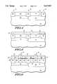
- FIG. 1Shown in FIG. 1, in cross-section, is a portion of a semiconductor substrate 12. Electrical isolation of CMOS transistors to be fabricated on substrate 12 is provided, in part, by two buried layers formed at a surface 14 of semiconductor substrate 12. Those skilled in the art will appreciate that in the fabrication of CMOS devices, it is necessary to provide isolation for an N-type device residing in a semiconductor substrate adjacent to a P-type device. The isolation of adjacent devices of opposite conductivity type requires that electrical isolation structures of a specific conductivity type be formed. Accordingly, for the purpose of illustration, a first buried layer 16 is an N+ buried layer, and a second buried layer 18 is a P+ buried layer.
- each buried layeris dependent upon the corresponding conductivity type of the MOS transistor to be fabricated above each buried layer.
- semiconductor substrate 12is a P-type semiconductor material.
- first and second buried layers 16 and 18are formed by ion implantation of dopants into semiconductor substrate 12.
- a photolithographic maskis placed on surface 14 and N-type dopants, such as arsenic or phosphorous, are implanted into substrate 12 to form first buried layer 16.
- a second photolithographic maskis placed on surface 14 and P-type dopants are implanted into semiconductor substrate 12 to form second buried layer 18.
- first and second buried layer 16 and 18an undoped epitaxial layer 20 is deposited to overlie surface 14, as illustrated in FIG. 2.
- Undoped epitaxial layer 20is preferably deposited to a thickness of about 1 to 2 microns.
- the deposition of undoped epitaxial layer 20 onto surface 14forms a structure in which first and second buried layers 16 and 18 are spaced away from an upper surface 22 of undoped epitaxial layer 20.
- first and second buried layers 16 and 18can also be fabricated after the deposition of undoped epitaxial layer 20 by using a high voltage ion implant process. Where a high-voltage implant process is used, a photolithographic mask is placed on upper surface 22 and dopants are implanted through undoped epitaxial layer 20 and into semiconductor substrate 12.
- a plurality of trenches 24are formed in undoped epitaxial layer 20, as illustrated in FIG. 3.
- Trenches 24are formed by placing a photolithographic mask on upper surface 22, then anisotropically etching undoped epitaxial layer 20. The etching process partitions undoped epitaxial layer 20 into a first active region 26 and a second active region 28.
- dielectric isolation regions 30are fabricated within the trenches 24.
- dielectric isolation regions 30are formed by the deposition of a dielectric 2material, such as silicon dioxide, onto upper surface 22 and filling trenches 24.
- a planarization processis carried out to remove dielectric material overlying upper surface 22, and leaving dielectric material in trenches 24. The planarization process forms a smooth surface across dielectric isolation regions 30 continuous with upper surface 22.
- dielectric isolation regions 30Upon formation of dielectric isolation regions 30, active regions 26 and 28 are electrically isolated from substrate 12, and from each other. As illustrated in FIG. 4, first buried layer 16 resides below first active region 26 and electrically separates first active region 26 from substrate 12. Additionally, dielectric isolation regions 30 bound first active region 26 electrically separating first active region 26 from remaining portions of undoped epitaxial layer 20. Correspondingly, second buried layer 18 resides below second active region 28 and electrically separates second active region 28 from semiconductor substrate 12. Also, dielectric isolation regions 30 bound second active region 28 and electrically separate second active region 28 from remaining portions of undoped epitaxial layer 20.
- a masking layer 32is formed to overlie upper surface 22.
- Masking layer 32includes a pad oxide layer 34 in contact with upper surface 22 and with dielectric isolation regions 30, and a silicon nitride layer 36 overlying pad oxide layer 34.
- pad oxide layer 34is differentially etchable with respect to silicon nitride layer 36. Accordingly, pad oxide layer 34 provides an etch-stop layer upon which silicon nitride layer 36 can be selectively patterned. Additionally, pad oxide layer 34 provides a buffer layer over first and second active regions 26 and 28, which prevents contamination of first and second active regions 26 and 28 during subsequent processing.
- masking layer 32is preferably a composite material, another material, which is differentially etchable with respect to silicon and silicon dioxide can also be employed.
- openings 38 and 40are positioned to expose channel regions 42 and 44 in active regions 26 and 28, respectively. Openings 38 and 40 are formed by placing a lithographic mask 47 on silicon nitride layer 36 and etching silicon nitride layer 36. Then, dopants are selectively implanted into active regions 26 and 28 through openings 38 and 40. An N-type dopant, such as phosphorous or arsenic, is selectively implanted through opening 38 to form channel region 42 in first active region 26.
- a P-type dopantsuch as boron
- boronis implanted through opening 40 into second active region 28 to form channel region 44 in second active region 28.
- the selective implantsare accomplished by masking off remaining portions of substrate 12 prior to performing each selective implant.
- channel regions 42 and 44are precisely self-aligned to openings 38 and 40, respectively.
- Channel regions 42 and 44are both bounded by intrinsic silicon in the remaining portions of active regions 26 and 28.
- channel regions 42 and 44extend from upper surface 22 to first and second buried layers 16 and 18, respectively.
- first and second gate electrodes 46 and 48are formed in openings 38 and 40, respectively, as illustrated in FIG. 7.
- Gate electrodes 46 and 48are preferably formed by depositing a gate forming material to overlie masking layer 32 and fill openings 38 and 40. Then, a planarization process is carried out to remove the gate forming material from the upper surface of masking layer 32, and to leave portions of the gate forming material in openings 38 and 40.
- the gate forming materialis polycrystalline silicon.
- another electrically conductive or semiconductive materialcan be used.
- first and second gate electrodes 46 and 48can be formed with a refractory metal, such as titanium, tungsten, molybdenum, and the like.
- the gate forming materialcan be a refractory metal silicide, such as titanium silicide, tungsten silicide, and the like.
- first and second gate electrodes 46 and 48does not include a critical lithographic alignment step.
- the gate electrodesare fully self-aligned to channel regions 42 and 44 through openings 38 and 40, respectively. After completing the implant process to form channel regions 42 and 44, portions of pad oxide layer 34 exposed by openings 38 and 40 are removed. Then, an oxidation process is carried out to form a gate dielectric material 45 overlying channel regions 42 and 44.
- first and second gate electrodes 46 and 48is completed by removing silicon nitride layer 36 and forming insulating sidewall spacers 50.
- silicon nitrideis deposited to overlie first and second gate electrodes 46 and 48. Then, the silicon nitride is anisotropically etched to form sidewall spacers 50 adjacent to the vertical edges of first and second gate electrodes 46 and 48.
- source drain extension regionscan be formed in active regions 26 and 28 prior to the formation of sidewall spacers 50.
- the source and drain extension regionsare preferably formed by a low dose, low energy ion implantation of P-type dopants into active region 26 and N-type dopants into active region 28. Once the implants are complete, sidewall spacers 50 are formed. In this context, sidewall spacers 50 will become an implant mask for the subsequent formation of heavily-doped source and drain regions.
- CMOS devicein accordance with the present embodiment of the invention is completed with the formation of heavily-doped source and drain regions in active regions 26 and 28, as illustrated in FIG. 9.
- substrate 12is selectively implanted with P-type dopants to form source and drain regions 52 and 53 in active region 26 on either side of first gate electrode 46.
- active region 28is selectively implanted with N-type dopants to form heavily-doped source and drain regions 54 and 55 in active region 28 on either side of second gate electrode 48. It is important to note that the ion implant processes used to form the source and drain regions create doped regions in active regions 26 and 28 having a peak concentration in the upper portion of the active regions.
- the source and drain regionsare self-aligned to the sidewall spacers adjacent to the gate electrodes and to the channel regions. Further, the range of implanted dopants is constrained to the upper portion of active regions 26 and 28 such that remaining portions 20' of undoped epitaxial layer 20 vertically separate the source and drain regions from first and second buried layer 16 and 18.
- Heavily-doped source and drain regions 52 and 53are formed by masking off remaining portions of substrate 12 and implanting P-type dopants, such as boron, into active region 26 using sidewall spacers 50 adjacent to first gate electrode 46 as a doping mask.
- the implant energy usedwill depend upon the deposition thickness of undoped epitaxial layer 20. For example, for a deposited thickness of 1 to 2 microns, a boron implant energy of about 10 to 20 keV can be used.
- N-type source and drain regions 54 and 55are formed by masking off remaining portions of semiconductor substrate 12 and implanting an N-type dopant, such as phosphorous or arsenic, into active region 28.
- sidewall spacers 50 adjacent to second gate electrode 48function as an implant mask.
- the deposited thickness of undoped epitaxial layer 20is about 1 to 2 microns, and arsenic is used to form source and drain regions 54 and 55, an implant energy of about 40 to 80 keV is used.
- the formation of source and drain regions 52 and 53completes the fabrication of a P-type MOS transistor in active region 26. Further, the formation of source and drain regions 54 and 55 complete the fabrication of an N-channel MOS transistor 58 in active region 28.
- remaining portion 20'composed of undoped, epitaxial silicon vertically separates the source and drain regions from first and second buried layers 16 and 18.
- the implant energyBy carefully controlling the implant energy, the range of dopants implanted into active regions 26 and 28 is constrained such that a maximum source and drain junction depth of about 0.1 to 0.2 microns is obtained. Meanwhile, the junction depth of first and second buried layers 16 and 18 is preferably about 0.3 to 0.4 microns. Accordingly, a region of intrinsic silicon remains vertically separating the source and drain regions from the buried layers.
- the undoped epitaxial layer underlying the source and drain regionsis comprised of silicon that is fully depleted of charge carriers. As a result of the vertical separation of the junctions, large capacitance across the electrical junction between the source drain regions and semiconductor substrate 12 does not arise.
- undoped siliconunderlies the source and drain regions of each transistor, the transistors are fully isolated from remaining portions of substrate 12 and from each other by first and second buried layers 16 and 18, and by dielectric isolation region 30.
- refractory metal silicide regions 60are formed in the source and drain regions at upper surface 22. Additionally, refractory metal silicide regions are also formed at the upper surface of first and second gate electrodes 46 and 48.
- refractory metal silicide regions 60are formed by first depositing a layer of refractory metal, followed by thermal annealing to react-the refractory metal with silicon in the source and drain regions and the gate electrodes.
- refractory metal silicide regions 60can be formed by the deposition of a layer of titanium followed by thermal annealing at a temperature of about 600° C. to 700° C.
- the refractory metal silicide forming processdoes not form refractory metal silicide over insulating sidewall spacers 50. Therefore, the refractory metal silicide regions residing at the upper surface of first and second gate electrodes 46 and 48 are electrically isolated from the refractory metal silicide at the surface of the source and drain regions.
- FIG. 10Shown in FIG. 10 is another embodiment of the invention in which one buried layer is configured as an annular region in substrate 12 subtending a portion of dielectric isolation region 30 surrounding N-channel MOS transistor 58.
- Annular buried layer 62is characterized by an internal diameter having a specified, predetermined distance in substrate 12.
- Annular buried layer 62functions in conjunction with dielectric isolation regions 30 to provide electrical isolation for N-channel MOS transistor 58.
- Annular buried layer 62is formed by confining implanted dopants to a region of semiconductor substrate 12 in which dielectric isolation region 30 is to be formed. The confinement of the buried layer to a region of substrate 12 in the vicinity of dielectric isolation regions 30 further enhances the performance of N-channel MOS transistor 58. By removing the high concentration of P-type dopants further away from source and drain regions 54 and 55, the junction capacitance is further reduced.
- FIG. 11Shown in FIG. 11 is yet another embodiment of the invention having recessed gate electrodes.
- the formation of MOS transistors 56 and 58reduces the depth of the source and drain regions relative to the channel region.
- the relative change in dimensions of the transistor elementseffectively reduces short-channel effects encountered in MOS transistors having sub-micron dimensions. Furthermore, the relative change in dimensions of the transistor elements reduces the series resistance in MOS transistors 56 and 58.
- active regions 26 and 28are etched using openings 38 and 40 in masking layer 32, as illustrated in FIG. 6.
- gate dielectric layer 45is grown to overlie the surfaces of the recess and the gate forming material is deposited to fill the recess in first active region 26 and second active region 28.
- insulating sidewall spacers 50extend into the recess and separate gate electrodes 46 and 48 from the source and drain regions.
Landscapes
- Metal-Oxide And Bipolar Metal-Oxide Semiconductor Integrated Circuits (AREA)
- Insulated Gate Type Field-Effect Transistor (AREA)
Abstract
Description
Related subject matter is disclosed in the commonly-assigned patent application entitled "Process for Fabricating a Fully Self-Aligned SOI MOS FET" having U.S. Ser. No. 08/497,317 and filed on even date.
This invention relates, in general, to a semiconductor device and a method for its fabrication, and more particularly, to a CMOS device incorporating epitaxial silicon layers and to a method for fabricating such a CMOS device.
In order to provide increased functional capability, integrated circuit devices are continually redesigned to smaller and smaller geometric dimensions. Although reducing transistor dimensions increases the functional performance of an integrated circuit, transistors can suffer a loss of performance when scaled to dimensions below one micron. The performance loss is especially acute in complementary-metal-oxide-semiconductor (CMOS) devices, which contain large numbers of diffused junctions.
As CMOS devices are continually scaled to dimensions below one micron, device reliability dictates a concomitant reduction in the power supply voltage. However, the reduction in physical dimensions coupled with the reduction in power supply voltage effectively reduces the transistor current. At reduced current levels, parasitic capacitances, such as drain junction capacitance and gate overlap capacitance, become significant factors contributing to low operating speed in transistor devices.
Performance degradation arising from short-channel effects represents an additional problem encountered as device dimensions are scaled below one micron. In particular, threshold voltage instability and current leakage can occur across the channel region of a metal-oxide-semiconductor (MOS) transistor having an effective channel length below one micron. Short-channel effects are typically addressed by selectively doping portions of the channel region, and by providing source and drain extensions adjacent to the channel region. Additionally, the substrate doping is often adjusted to compensate for the additional channel doping used to combat the short-channel effects.
While increased doping of the substrate and the channel region forestalls the onset of short-channel behavior in sub-micron CMOS devices, the additional dopants increase parasitic capacitances in the device. One solution to the parasitic capacitance problem is the fabrication of transistor devices in a silicon-on-insulator (SOI) substrate. The buried oxide layer of the SOI substrate effectively separates the junctions associated with the transistors from the underlying semiconductor substrate. The junction capacitance is reduced by increasing the separation distance between regions of high dopant concentration. For example, the buried oxide layer in an SOI device separates active transistor regions from the silicon substrate, thus reducing junction capacitance. Although buried oxide layers are effective at reducing junction capacitance, SOI substrates are expensive to produce and increase the unit cost of CMOS devices fabricated in SOI substrates. Accordingly, a need existed for a CMOS device and fabrication process using conventional silicon technology, yet achieving reduced junction capacitance at device geometries below one micron.
In practicing the present invention there is provided a CMOS device having reduced junction capacitance and a process for the fabrication of the device. The junction capacitance is reduced by eliminating well regions typically used in CMOS device fabrication for electrical isolation of MOS transistors. In the present invention, intrinsic silicon is provided below the source and drain regions of N-channel and P-channel transistors. The intrinsic silicon vertically separates the source and drain regions of the MOS transistors from buried layers underlying the transistors.
In one embodiment of the invention, a semiconductor substrate is provided having an undoped epitaxial layer overlying a buried layer. A masking layer is formed on the undoped epitaxial layer. The masking layer has an opening therein exposing a channel portion of the undoped epitaxial layer. The channel portion is doped with a dopant of a first conductivity type using the opening in the masking layer as a doping mask. A gate electrode is formed in the opening and source and drain regions are formed in the undoped epitaxial layer on either side of the gate electrode. The source and drain regions are formed such that a portion of the undoped epitaxial layer vertically separates the source and drain regions from the buried layer. By removing regions of high dopant concentration away from the source and drain junctions, the junction capacitance is minimized. The reduction of junction capacitance results in higher operating speed for both N-channel and P-channel transistors fabricated in accordance with the invention.
FIGS. 1-9 illustrate, in cross-section, process steps for the fabrication of a CMOS device in accordance with one embodiment of the invention;
FIG. 10 illustrates, in cross-section, another embodiment of the invention having a separated buried layer; and
FIG. 11 illustrates, in cross-section, yet another embodiment of the invention having recessed gate electrodes.
It will be appreciated that for simplicity and clarity of illustration, elements shown in the FIGURES have not necessarily been drawn to scale. For example, the dimensions of some of the elements are exaggerated relative to each other. Further, where considered appropriate, reference numerals have been repeated among the FIGURES to indicate corresponding elements.
The present invention provides a CMOS device, and process for fabricating the device, having high operating speed at supply voltages of less than 5 volts. Integrated circuits incorporating the device of the invention exhibit reduced stage delay at operating voltages in the range of about 3.3 to about 1.8 volts. Improved operational speed is obtained through a reduction in the junction capacitance and the overlap capacitance of transistors fabricated in accordance with the invention. Reduced junction capacitance is obtained by elimination of the well region employed in CMOS devices of the prior art. The well region is replaced by buried layers within the substrate that are separated from the source and drain regions by fully-depleted, undoped silicon. Additionally, the process of the invention provides CMOS transistors having fully self-aligned channel regions under the gate electrode. The fabrication of CMOS transistors having fully self-aligned channel regions further reduces the junction capacitance of the device. These and other advantages of the invention will become more fully understood following a description of one embodiment of a fabrication process in accordance with the invention.
Shown in FIG. 1, in cross-section, is a portion of asemiconductor substrate 12. Electrical isolation of CMOS transistors to be fabricated onsubstrate 12 is provided, in part, by two buried layers formed at asurface 14 ofsemiconductor substrate 12. Those skilled in the art will appreciate that in the fabrication of CMOS devices, it is necessary to provide isolation for an N-type device residing in a semiconductor substrate adjacent to a P-type device. The isolation of adjacent devices of opposite conductivity type requires that electrical isolation structures of a specific conductivity type be formed. Accordingly, for the purpose of illustration, a first buriedlayer 16 is an N+ buried layer, and a second buriedlayer 18 is a P+ buried layer. Furthermore, those skilled in the art will appreciate that the specific conductivity type of each buried layer is dependent upon the corresponding conductivity type of the MOS transistor to be fabricated above each buried layer. Although the present embodiment illustrates paired N-channel and P-channel transistors, individual transistors can be fabricated by the process of the invention. In the present embodiment,semiconductor substrate 12 is a P-type semiconductor material.
In one method, first and second buriedlayers semiconductor substrate 12. A photolithographic mask is placed onsurface 14 and N-type dopants, such as arsenic or phosphorous, are implanted intosubstrate 12 to form first buriedlayer 16. Then, a second photolithographic mask is placed onsurface 14 and P-type dopants are implanted intosemiconductor substrate 12 to form second buriedlayer 18.
After forming first and second buriedlayer epitaxial layer 20 is deposited to overliesurface 14, as illustrated in FIG. 2. Undopedepitaxial layer 20 is preferably deposited to a thickness of about 1 to 2 microns. The deposition ofundoped epitaxial layer 20 ontosurface 14 forms a structure in which first and second buried layers 16 and 18 are spaced away from anupper surface 22 ofundoped epitaxial layer 20. Those skilled in the art will recognize that first and second buried layers 16 and 18 can also be fabricated after the deposition ofundoped epitaxial layer 20 by using a high voltage ion implant process. Where a high-voltage implant process is used, a photolithographic mask is placed onupper surface 22 and dopants are implanted throughundoped epitaxial layer 20 and intosemiconductor substrate 12.
Following the formation ofundoped epitaxial layer 20, a plurality oftrenches 24 are formed inundoped epitaxial layer 20, as illustrated in FIG. 3.Trenches 24 are formed by placing a photolithographic mask onupper surface 22, then anisotropically etchingundoped epitaxial layer 20. The etching process partitions undopedepitaxial layer 20 into a firstactive region 26 and a secondactive region 28.
Oncetrenches 24 are formed, a plurality ofdielectric isolation regions 30 are fabricated within thetrenches 24. Preferably,dielectric isolation regions 30 are formed by the deposition of a dielectric 2material, such as silicon dioxide, ontoupper surface 22 and fillingtrenches 24. Next, a planarization process is carried out to remove dielectric material overlyingupper surface 22, and leaving dielectric material intrenches 24. The planarization process forms a smooth surface acrossdielectric isolation regions 30 continuous withupper surface 22.
Upon formation ofdielectric isolation regions 30,active regions substrate 12, and from each other. As illustrated in FIG. 4, first buriedlayer 16 resides below firstactive region 26 and electrically separates firstactive region 26 fromsubstrate 12. Additionally,dielectric isolation regions 30 bound firstactive region 26 electrically separating firstactive region 26 from remaining portions ofundoped epitaxial layer 20. Correspondingly, second buriedlayer 18 resides below secondactive region 28 and electrically separates secondactive region 28 fromsemiconductor substrate 12. Also,dielectric isolation regions 30 bound secondactive region 28 and electrically separate secondactive region 28 from remaining portions ofundoped epitaxial layer 20.
Referring to FIG. 5, amasking layer 32 is formed to overlieupper surface 22. Maskinglayer 32 includes apad oxide layer 34 in contact withupper surface 22 and withdielectric isolation regions 30, and asilicon nitride layer 36 overlyingpad oxide layer 34. In maskinglayer 32,pad oxide layer 34 is differentially etchable with respect tosilicon nitride layer 36. Accordingly,pad oxide layer 34 provides an etch-stop layer upon whichsilicon nitride layer 36 can be selectively patterned. Additionally,pad oxide layer 34 provides a buffer layer over first and secondactive regions active regions layer 32 is preferably a composite material, another material, which is differentially etchable with respect to silicon and silicon dioxide can also be employed.
Once maskinglayer 32 is formed, the masking layer is patterned to formopenings Openings channel regions active regions Openings lithographic mask 47 onsilicon nitride layer 36 and etchingsilicon nitride layer 36. Then, dopants are selectively implanted intoactive regions openings channel region 42 in firstactive region 26. Correspondingly, a P-type dopant such as boron, is implanted through opening 40 into secondactive region 28 to formchannel region 44 in secondactive region 28. The selective implants are accomplished by masking off remaining portions ofsubstrate 12 prior to performing each selective implant. Following the ion implant process,channel regions openings Channel regions active regions channel regions upper surface 22 to first and second buried layers 16 and 18, respectively.
After formingchannel regions second gate electrodes openings Gate electrodes layer 32 and fillopenings layer 32, and to leave portions of the gate forming material inopenings second gate electrodes
It is important to note that the process used to fabricate first andsecond gate electrodes regions openings channel regions pad oxide layer 34 exposed byopenings gate dielectric material 45 overlyingchannel regions
Referring to FIG. 8, the fabrication of first andsecond gate electrodes silicon nitride layer 36 and forming insulatingsidewall spacers 50. In one method, silicon nitride is deposited to overlie first andsecond gate electrodes sidewall spacers 50 adjacent to the vertical edges of first andsecond gate electrodes active regions sidewall spacers 50. The source and drain extension regions are preferably formed by a low dose, low energy ion implantation of P-type dopants intoactive region 26 and N-type dopants intoactive region 28. Once the implants are complete,sidewall spacers 50 are formed. In this context,sidewall spacers 50 will become an implant mask for the subsequent formation of heavily-doped source and drain regions.
The fabrication of a CMOS device in accordance with the present embodiment of the invention is completed with the formation of heavily-doped source and drain regions inactive regions sidewall spacers 50 are formed,substrate 12 is selectively implanted with P-type dopants to form source and drainregions active region 26 on either side offirst gate electrode 46. Correspondingly,active region 28 is selectively implanted with N-type dopants to form heavily-doped source and drainregions active region 28 on either side ofsecond gate electrode 48. It is important to note that the ion implant processes used to form the source and drain regions create doped regions inactive regions active regions undoped epitaxial layer 20 vertically separate the source and drain regions from first and second buriedlayer
Heavily-doped source and drainregions substrate 12 and implanting P-type dopants, such as boron, intoactive region 26 usingsidewall spacers 50 adjacent tofirst gate electrode 46 as a doping mask. The implant energy used will depend upon the deposition thickness ofundoped epitaxial layer 20. For example, for a deposited thickness of 1 to 2 microns, a boron implant energy of about 10 to 20 keV can be used. Correspondingly, N-type source and drainregions semiconductor substrate 12 and implanting an N-type dopant, such as phosphorous or arsenic, intoactive region 28. Again,sidewall spacers 50 adjacent tosecond gate electrode 48 function as an implant mask. Where the deposited thickness ofundoped epitaxial layer 20 is about 1 to 2 microns, and arsenic is used to form source and drainregions regions active region 26. Further, the formation of source and drainregions channel MOS transistor 58 inactive region 28.
Upon completion of the source drain formation process, remaining portion 20' composed of undoped, epitaxial silicon vertically separates the source and drain regions from first and second buried layers 16 and 18. By carefully controlling the implant energy, the range of dopants implanted intoactive regions
Those skilled in the art will recognize that separating the source and drain regions from the buried layers by a region of intrinsic, undoped silicon will reduce the junction capacitance between the source drain regions and underlying silicon. The undoped epitaxial layer underlying the source and drain regions is comprised of silicon that is fully depleted of charge carriers. As a result of the vertical separation of the junctions, large capacitance across the electrical junction between the source drain regions andsemiconductor substrate 12 does not arise. Although undoped silicon underlies the source and drain regions of each transistor, the transistors are fully isolated from remaining portions ofsubstrate 12 and from each other by first and second buried layers 16 and 18, and bydielectric isolation region 30.
After formation of the source and drain regions, refractorymetal silicide regions 60 are formed in the source and drain regions atupper surface 22. Additionally, refractory metal silicide regions are also formed at the upper surface of first andsecond gate electrodes metal silicide regions 60 are formed by first depositing a layer of refractory metal, followed by thermal annealing to react-the refractory metal with silicon in the source and drain regions and the gate electrodes. For example, refractorymetal silicide regions 60 can be formed by the deposition of a layer of titanium followed by thermal annealing at a temperature of about 600° C. to 700° C. The refractory metal silicide forming process does not form refractory metal silicide over insulatingsidewall spacers 50. Therefore, the refractory metal silicide regions residing at the upper surface of first andsecond gate electrodes
Shown in FIG. 10 is another embodiment of the invention in which one buried layer is configured as an annular region insubstrate 12 subtending a portion ofdielectric isolation region 30 surrounding N-channel MOS transistor 58. Annular buriedlayer 62 is characterized by an internal diameter having a specified, predetermined distance insubstrate 12. Annular buriedlayer 62 functions in conjunction withdielectric isolation regions 30 to provide electrical isolation for N-channel MOS transistor 58. Annular buriedlayer 62 is formed by confining implanted dopants to a region ofsemiconductor substrate 12 in whichdielectric isolation region 30 is to be formed. The confinement of the buried layer to a region ofsubstrate 12 in the vicinity ofdielectric isolation regions 30 further enhances the performance of N-channel MOS transistor 58. By removing the high concentration of P-type dopants further away from source and drainregions
Shown in FIG. 11 is yet another embodiment of the invention having recessed gate electrodes. The formation ofMOS transistors MOS transistors
To form the recessed gate electrodes,active regions openings layer 32, as illustrated in FIG. 6. After etching a recess intoactive regions gate dielectric layer 45 is grown to overlie the surfaces of the recess and the gate forming material is deposited to fill the recess in firstactive region 26 and secondactive region 28. Subsequent processing continues as described for the fabrication of the embodiment illustrated in FIG. 9. To further reduce the parasitic capacitance inMOS transistors sidewall spacers 50 extend into the recess andseparate gate electrodes
Thus it is apparent that there has been provided, in accordance with the invention, a CMOS device having reduced parasitic capacitance and a fabrication process which fully meets the advantages set forth above. Although the invention has been described and illustrated with reference to specific illustrative embodiments thereof, it is not intended that the invention be limited to those illustrative embodiments. Those skilled in the art will recognize that variations and modifications can be made without departing from the spirit of the invention. For example, a conventional LOCOS isolation process can be used to form the dielectric isolation regions. It is therefore intended to include within the invention all such variations and modifications as fall within the scope of the appended claims and equivalents thereof.
Claims (13)
1. A process for fabricating a semiconductor device comprising the steps of:
providing a semiconductor substrate having an undoped silicon layer overlying a buried layer;
forming a trench isolation structure in the undoped silicon layer to define an active region therein;
forming a masking layer on the undoped silicon layer, the masking layer having an opening therein exposing a channel portion of the active region;
doping the channel portion with a first dopant, using the masking layer as a doping mask, wherein the first dopant extends from an upper surface of the undoped silicon layer to the buried layer;
depositing a layer of polycrystalline silicon to overlie the masking layer and the channel portion;
planarizing the polycrystalline silicon to form a gate electrode overlying the channel portion;
removing the masking layer; and
forming source and drain regions in the undoped silicon layer on either side of the gate electrode, wherein the source and drain regions are vertically separated from the buried layer by a portion of the undoped silicon layer.
2. The process of claim 1, wherein the step of forming source and drain regions comprises ion implantation of dopant species, wherein the undoped silicon layer is deposited to a first thickness, and wherein the source region has a maximum junction depth which is less than the first thickness of the undoped silicon layer the drain region has a maximum junction depth which is less than the first thickness of the undoped silicon layer.
3. The process of claim 1 further comprising the step of etching a recess in the channel portion of the undoped silicon layer using the masking layer as an etching mask.
4. The process of claim 3 further comprising the step of forming insulating sidewall spacers adjacent to the gate electrode.
5. The process of claim 1, wherein the steps of providing a buried layer and forming a trench isolation structure comprise:
implanting the semiconductor substrate with a second dopant to form an annular doped region in the semiconductor substrate; and
etching a trench in the undoped epitaxial layer such that the trench is subtended by the annular doped region.
6. A process for fabricating a semiconductor device comprising the steps of:
providing a semiconductor substrate having an undoped epitaxial layer overlying a buried layer of a first conductivity type;
forming a masking layer on the undoped epitaxial layer, the masking layer having an opening therein exposing a channel portion of the undoped epitaxial layer;
doping the channel portion with a dopant of the first conductivity type, using the masking layer as a doping mask;
forming a gate electrode in the opening; and
forming source and drain regions in the undoped epitaxial layer on either side of the gate electrode, wherein the source and drain regions are vertically separated from the buried layer by a portion of the undoped epitaxial layer.
7. The process of claim 6, wherein the step of doping the channel portion comprises forming a continuous doped region extending from an upper surface of the undoped epitaxial layer to the buried layer.
8. The process of claim 6, further comprising the step of forming a dielectric isolation region in the undoped epitaxial layer, and wherein the step of providing a buried layer comprises forming a continuous doped region subtending the dielectric isolation region.
9. The process of claim 6 further comprising the step of etching a recess in the channel portion of the undoped epitaxial layer using the masking layer as an etching mask.
10. A process for fabricating a semiconductor device comprising the steps of:
providing a semiconductor substrate having a surface; forming a first buried layer of a first conductivity type at the surface;
forming a second buried layer of a second conductivity type at the surface adjacent to the first buried layer;
forming an undoped epitaxial layer overlying the first and second buried layers;
forming an isolation region in the undoped epitaxial layer to define a first active region overlying the first buried layer and a second active region overlying the second buried layer;
forming a masking pattern overlying the undoped epitaxial layer and the isolation region, the masking pattern having a first opening therein exposing a channel portion of the first active region and a second opening therein exposing a channel portion of the second active region;
doping the channel portion of the first active region with a dopant of the first conductivity type;
doping the channel portion of the second active region with a dopant of the second conductivity type;
forming a first gate electrode in the first opening and a second gate electrode in the second opening;
forming source and drain regions of the second conductivity type on either side of the first gate electrode; and
forming source and drain regions of the first conductivity type on either side of the second gate electrode,
wherein the source and drain regions of the second conductivity type are spaced apart from the first buried layer by a first portion of the undoped epitaxial layer, and
wherein the source and drain regions of the first conductivity type are spaced apart frozen the second buried layer by a second portion of the undoped epitaxial layer.
11. The process of claim 10, wherein a portion of the isolation region surrounds the second active region, and wherein the step of forming a second buried layer comprises forming a continuous doped region subtending the portion of the isolation region.
12. The process of claim 10, wherein the step of doping the channel portion of the first active region comprises forming a doped region extending from the surface of the undoped epitaxial layer to the first buried layer.
13. The process of claim 10, wherein the step of doping the channel portion of the second active region comprises forming a doped region extending from the surface of the undoped epitaxial layer to the second buried layer.
Priority Applications (1)
| Application Number | Priority Date | Filing Date | Title |
|---|---|---|---|
| US08/498,709US5627097A (en) | 1995-07-03 | 1995-07-03 | Method for making CMOS device having reduced parasitic capacitance |
Applications Claiming Priority (1)
| Application Number | Priority Date | Filing Date | Title |
|---|---|---|---|
| US08/498,709US5627097A (en) | 1995-07-03 | 1995-07-03 | Method for making CMOS device having reduced parasitic capacitance |
Publications (1)
| Publication Number | Publication Date |
|---|---|
| US5627097Atrue US5627097A (en) | 1997-05-06 |
Family
ID=23982173
Family Applications (1)
| Application Number | Title | Priority Date | Filing Date |
|---|---|---|---|
| US08/498,709Expired - Fee RelatedUS5627097A (en) | 1995-07-03 | 1995-07-03 | Method for making CMOS device having reduced parasitic capacitance |
Country Status (1)
| Country | Link |
|---|---|
| US (1) | US5627097A (en) |
Cited By (32)
| Publication number | Priority date | Publication date | Assignee | Title |
|---|---|---|---|---|
| US5783486A (en)* | 1996-10-18 | 1998-07-21 | Vanguard International Semiconductor Corporation | Bridge-free self aligned silicide process |
| US5864158A (en)* | 1997-04-04 | 1999-01-26 | Advanced Micro Devices, Inc. | Trench-gated vertical CMOS device |
| US6010928A (en)* | 1997-05-03 | 2000-01-04 | United Microelectronics Corp. | High density transistor component and its manufacturing method |
| US6144086A (en)* | 1999-04-30 | 2000-11-07 | International Business Machines Corporation | Structure for improved latch-up using dual depth STI with impurity implant |
| US6150687A (en)* | 1997-07-08 | 2000-11-21 | Micron Technology, Inc. | Memory cell having a vertical transistor with buried source/drain and dual gates |
| US6156607A (en)* | 1997-10-06 | 2000-12-05 | Micron Technology, Inc. | Method for a folded bit line memory using trench plate capacitor cells with body bias contacts |
| US6156604A (en)* | 1997-10-06 | 2000-12-05 | Micron Technology, Inc. | Method for making an open bit line memory cell with a vertical transistor and trench plate trench capacitor |
| US6165836A (en)* | 1997-10-06 | 2000-12-26 | Micron Technology, Inc. | Circuit and method for an open bit line memory cell with a vertical transistor and trench plate trench capacitor |
| US6239472B1 (en)* | 1998-09-01 | 2001-05-29 | Philips Electronics North America Corp. | MOSFET structure having improved source/drain junction performance |
| US6242775B1 (en)* | 1998-02-24 | 2001-06-05 | Micron Technology, Inc. | Circuits and methods using vertical complementary transistors |
| US6317357B1 (en) | 1998-02-24 | 2001-11-13 | Micron Technology, Inc. | Vertical bipolar read access for low voltage memory cell |
| US6410378B2 (en)* | 1997-07-22 | 2002-06-25 | Micron Technonlogy, Inc. | Method of fabrication of semiconductor structures by ion implantation |
| US6437377B1 (en) | 2001-01-24 | 2002-08-20 | International Business Machines Corporation | Low dielectric constant sidewall spacer using notch gate process |
| US6486703B2 (en) | 1998-08-04 | 2002-11-26 | Micron Technology, Inc. | Programmable logic array with vertical transistors |
| US20030008438A1 (en)* | 2000-11-15 | 2003-01-09 | Abbott Todd R. | Method of forming a field effect transistor |
| US20030122155A1 (en)* | 2001-12-27 | 2003-07-03 | Tatsuya Ohguro | Semiconductor device applied to a variable capacitance capacitor and amplifier |
| US6653700B2 (en) | 2001-06-29 | 2003-11-25 | Intel Corporation | Transistor structure and method of fabrication |
| US6812516B2 (en) | 1998-02-27 | 2004-11-02 | Micron Technology, Inc. | Field programmable logic arrays with vertical transistors |
| US20040235243A1 (en)* | 1997-10-06 | 2004-11-25 | Micron Technology, Inc. | Circuit and method for a folded bit line memory cell with vertical transistor and trench capacitor |
| US20050029682A1 (en)* | 2003-08-07 | 2005-02-10 | Kwan-Ju Koh | MOS transistor and fabrication method thereof |
| US20050035407A1 (en)* | 2003-08-12 | 2005-02-17 | Kwan-Ju Koh | Semiconductor devices and methods of fabricating the same |
| US20050095756A1 (en)* | 2002-08-15 | 2005-05-05 | Tang Sanh D. | Method of forming a field effect transistor |
| US20060022267A1 (en)* | 2003-12-29 | 2006-02-02 | Shigenobu Maeda | Semiconductor device and method of manufacturing the semiconductor device |
| US20060249777A1 (en)* | 1998-01-22 | 2006-11-09 | Micron Technology, Inc. | Device, system, and method for a trench capacitor having micro-roughened semiconductor surfaces |
| US20070155142A1 (en)* | 2005-12-30 | 2007-07-05 | Been-Yih Jin | Abrupt junction formation by atomic layer epitaxy of in situ delta doped dopant diffusion barriers |
| US20070215940A1 (en)* | 2006-03-16 | 2007-09-20 | Spansion Llc | Vertical semiconductor device |
| US20080142840A1 (en)* | 2004-09-29 | 2008-06-19 | Nick Lindert | Metal gate transistors with epitaxial source and drain regions |
| US7442614B1 (en)* | 2008-03-21 | 2008-10-28 | International Business Machines Corporation | Silicon on insulator devices having body-tied-to-source and methods of making |
| US20090191683A1 (en)* | 2004-06-17 | 2009-07-30 | Samsung Electronics Co., Ltd. | Method of forming transistor having channel region at sidewall of channel portion hole |
| US8704311B2 (en)* | 2011-03-04 | 2014-04-22 | Fujitsu Semiconductor Limited | Semiconductor device having epitaxial semiconductor layer above impurity layer |
| US20170250263A1 (en)* | 2015-02-19 | 2017-08-31 | International Business Machines Corporation | Non-uniform gate dielectric for u-shape mosfet |
| US10515801B2 (en) | 2007-06-04 | 2019-12-24 | Micron Technology, Inc. | Pitch multiplication using self-assembling materials |
Citations (20)
| Publication number | Priority date | Publication date | Assignee | Title |
|---|---|---|---|---|
| US3948694A (en)* | 1975-04-30 | 1976-04-06 | Motorola, Inc. | Self-aligned method for integrated circuit manufacture |
| US4830980A (en)* | 1988-04-22 | 1989-05-16 | Hughes Aircraft Company | Making complementary integrated p-MODFET and n-MODFET |
| US4845537A (en)* | 1986-12-01 | 1989-07-04 | Mitsubishi Denki Kabushiki Kaisha | Vertical type MOS transistor and method of formation thereof |
| US4864374A (en)* | 1987-11-30 | 1989-09-05 | Texas Instruments Incorporated | Two-transistor dram cell with high alpha particle immunity |
| US4868135A (en)* | 1988-12-21 | 1989-09-19 | International Business Machines Corporation | Method for manufacturing a Bi-CMOS device |
| US4874718A (en)* | 1987-07-28 | 1989-10-17 | Mitsubishi Denki Kabushiki Kaisha | Method for forming SOI film |
| US4902639A (en)* | 1989-08-03 | 1990-02-20 | Motorola, Inc. | Process for making BiCMOS integrated circuit having a shallow trench bipolar transistor with vertical base contacts |
| US4957874A (en)* | 1987-11-27 | 1990-09-18 | Nec Corporation | Self-aligned Bi-CMOS device having high operation speed and high integration density |
| US4963502A (en)* | 1988-08-25 | 1990-10-16 | Texas Instruments, Incorporated | Method of making oxide-isolated source/drain transistor |
| US5015594A (en)* | 1988-10-24 | 1991-05-14 | International Business Machines Corporation | Process of making BiCMOS devices having closely spaced device regions |
| US5108945A (en)* | 1990-01-10 | 1992-04-28 | Microunity Systems Engineering, Inc. | Process for fabricating polysilicon resistors and interconnects |
| US5110757A (en)* | 1990-12-19 | 1992-05-05 | North American Philips Corp. | Formation of composite monosilicon/polysilicon layer using reduced-temperature two-step silicon deposition |
| US5124768A (en)* | 1982-04-13 | 1992-06-23 | Seiko Epson Corporation | Thin film transistor and active matrix assembly including same |
| US5137837A (en)* | 1990-08-20 | 1992-08-11 | Hughes Aircraft Company | Radiation-hard, high-voltage semiconductive device structure fabricated on SOI substrate |
| US5158900A (en)* | 1991-10-18 | 1992-10-27 | Hewlett-Packard Company | Method of separately fabricating a base/emitter structure of a BiCMOS device |
| US5166084A (en)* | 1991-09-03 | 1992-11-24 | Motorola, Inc. | Process for fabricating a silicon on insulator field effect transistor |
| US5273921A (en)* | 1991-12-27 | 1993-12-28 | Purdue Research Foundation | Methods for fabricating a dual-gated semiconductor-on-insulator field effect transistor |
| US5336926A (en)* | 1992-02-25 | 1994-08-09 | Microunity Systems Engineering, Inc. | Bipolar junction exhibiting suppressed kirk effect |
| US5453390A (en)* | 1992-03-30 | 1995-09-26 | Nippondenso Co., Ltd. | Method of producing semiconductor device with current detecting function |
| US5504364A (en)* | 1993-01-04 | 1996-04-02 | Vlsi Technology, Inc. | CMOS locos isolation for self-aligned NPN BJT in a BiCMOS process |
- 1995
- 1995-07-03USUS08/498,709patent/US5627097A/ennot_activeExpired - Fee Related
Patent Citations (20)
| Publication number | Priority date | Publication date | Assignee | Title |
|---|---|---|---|---|
| US3948694A (en)* | 1975-04-30 | 1976-04-06 | Motorola, Inc. | Self-aligned method for integrated circuit manufacture |
| US5124768A (en)* | 1982-04-13 | 1992-06-23 | Seiko Epson Corporation | Thin film transistor and active matrix assembly including same |
| US4845537A (en)* | 1986-12-01 | 1989-07-04 | Mitsubishi Denki Kabushiki Kaisha | Vertical type MOS transistor and method of formation thereof |
| US4874718A (en)* | 1987-07-28 | 1989-10-17 | Mitsubishi Denki Kabushiki Kaisha | Method for forming SOI film |
| US4957874A (en)* | 1987-11-27 | 1990-09-18 | Nec Corporation | Self-aligned Bi-CMOS device having high operation speed and high integration density |
| US4864374A (en)* | 1987-11-30 | 1989-09-05 | Texas Instruments Incorporated | Two-transistor dram cell with high alpha particle immunity |
| US4830980A (en)* | 1988-04-22 | 1989-05-16 | Hughes Aircraft Company | Making complementary integrated p-MODFET and n-MODFET |
| US4963502A (en)* | 1988-08-25 | 1990-10-16 | Texas Instruments, Incorporated | Method of making oxide-isolated source/drain transistor |
| US5015594A (en)* | 1988-10-24 | 1991-05-14 | International Business Machines Corporation | Process of making BiCMOS devices having closely spaced device regions |
| US4868135A (en)* | 1988-12-21 | 1989-09-19 | International Business Machines Corporation | Method for manufacturing a Bi-CMOS device |
| US4902639A (en)* | 1989-08-03 | 1990-02-20 | Motorola, Inc. | Process for making BiCMOS integrated circuit having a shallow trench bipolar transistor with vertical base contacts |
| US5108945A (en)* | 1990-01-10 | 1992-04-28 | Microunity Systems Engineering, Inc. | Process for fabricating polysilicon resistors and interconnects |
| US5137837A (en)* | 1990-08-20 | 1992-08-11 | Hughes Aircraft Company | Radiation-hard, high-voltage semiconductive device structure fabricated on SOI substrate |
| US5110757A (en)* | 1990-12-19 | 1992-05-05 | North American Philips Corp. | Formation of composite monosilicon/polysilicon layer using reduced-temperature two-step silicon deposition |
| US5166084A (en)* | 1991-09-03 | 1992-11-24 | Motorola, Inc. | Process for fabricating a silicon on insulator field effect transistor |
| US5158900A (en)* | 1991-10-18 | 1992-10-27 | Hewlett-Packard Company | Method of separately fabricating a base/emitter structure of a BiCMOS device |
| US5273921A (en)* | 1991-12-27 | 1993-12-28 | Purdue Research Foundation | Methods for fabricating a dual-gated semiconductor-on-insulator field effect transistor |
| US5336926A (en)* | 1992-02-25 | 1994-08-09 | Microunity Systems Engineering, Inc. | Bipolar junction exhibiting suppressed kirk effect |
| US5453390A (en)* | 1992-03-30 | 1995-09-26 | Nippondenso Co., Ltd. | Method of producing semiconductor device with current detecting function |
| US5504364A (en)* | 1993-01-04 | 1996-04-02 | Vlsi Technology, Inc. | CMOS locos isolation for self-aligned NPN BJT in a BiCMOS process |
Non-Patent Citations (24)
| Title |
|---|
| Inaba, et al., "Inverter Performance of 0.10μm CMOS Operating at Room Temperature", Dec. 1994 IEEE Transactions On Electron Devices, vol. 41, No. 12, pp. 2399-2404. |
| Inaba, et al., Inverter Performance of 0.10 m CMOS Operating at Room Temperature , Dec. 1994 IEEE Transactions On Electron Devices, vol. 41, No. 12, pp. 2399 2404.* |
| Kusunoki, et al., "Hot-Carrier-Resistant Structure by Re-Oxidized Nitrided Oxide Sidewall for Highly Reliable and High Performance LDD MOSFETs", 1991 IEEE, pp. 25.4.1-25.4.4. |
| Kusunoki, et al., Hot Carrier Resistant Structure by Re Oxidized Nitrided Oxide Sidewall for Highly Reliable and High Performance LDD MOSFETs , 1991 IEEE, pp. 25.4.1 25.4.4.* |
| Lee et al., "A New 0.25-μm Recessed-Channel MOSFET with Selectively Halo-Doped Channel and Deep Graded Source/Drain", Dec. 1993 IEEE Electron Device Ltrs., vol. 14, No. 12, pp. 578-580. |
| Lee et al., A New 0.25 m Recessed Channel MOSFET with Selectively Halo Doped Channel and Deep Graded Source/Drain , Dec. 1993 IEEE Electron Device Ltrs., vol. 14, No. 12, pp. 578 580.* |
| Lee, et al., "Room Temperature 0.1μm CMOS Technology With 11.8 ps Gate Delay", 1993 IEDM, pp. 6.5.1-6.5.4. |
| Lee, et al., Room Temperature 0.1 m CMOS Technology With 11.8 ps Gate Delay , 1993 IEDM, pp. 6.5.1 6.5.4.* |
| Mikosha, et al., "A Novel CMOS Process Utilizing After-Gate-Implantation Process", pp. 41-42. |
| Mikosha, et al., A Novel CMOS Process Utilizing After Gate Implantation Process , pp. 41 42.* |
| Nguyen, et al., "Quasi-'SOI MOSFETs Using Selective Epitaxy and Polishing", 1992 IEEE, pp. 13.2.1-13.2.4. |
| Nguyen, et al., Quasi SOI MOSFETs Using Selective Epitaxy and Polishing , 1992 IEEE, pp. 13.2.1 13.2.4.* |
| Pfiester, et al., "A Self-Aligned LDD/Channel Implanted ITLDD Process with Selectively Deposited Poly Gates for CMOS VLSI", 1989 IEEE, pp. 32.2.1-32.2.4. |
| Pfiester, et al., "An ITLDD CMOS Process with Self-Aligned Reverse-Sequence LDD/Channel Implantation", Nov. 1991 IEEE Transactions On Electron Dev., vol. 38, No. 11, pp. 2460-2464. |
| Pfiester, et al., A Self Aligned LDD/Channel Implanted ITLDD Process with Selectively Deposited Poly Gates for CMOS VLSI , 1989 IEEE, pp. 32.2.1 32.2.4.* |
| Pfiester, et al., An ITLDD CMOS Process with Self Aligned Reverse Sequence LDD/Channel Implantation , Nov. 1991 IEEE Transactions On Electron Dev., vol. 38, No. 11, pp. 2460 2464.* |
| Shimizu, et al., "0.15 μm CMOS Process for High Performance and High Reliability", 1994 IEEE, pp. 4.1.1-4.1.4. |
| Shimizu, et al., 0.15 m CMOS Process for High Performance and High Reliability , 1994 IEEE, pp. 4.1.1 4.1.4.* |
| Tsui, et al., "Poly Reoxidation Time and Temperature Effects on Reverse Short Channel Characteristics", pp. 1-13. |
| Tsui, et al., Poly Reoxidation Time and Temperature Effects on Reverse Short Channel Characteristics , pp. 1 13.* |
| Wen, et al., "A Fully Planarized 0.25 μm CMOS Technology", pp. 83-84. |
| Wen, et al., A Fully Planarized 0.25 m CMOS Technology , pp. 83 84.* |
| Yoshimura, et al., "New CMOS Shallow Junction Well FET Structure (CMOS-SJET) for Low Power-Supply Voltage", 1992 IEDM, pp. 35.8.1-35.8.4. |
| Yoshimura, et al., New CMOS Shallow Junction Well FET Structure (CMOS SJET) for Low Power Supply Voltage , 1992 IEDM, pp. 35.8.1 35.8.4.* |
Cited By (72)
| Publication number | Priority date | Publication date | Assignee | Title |
|---|---|---|---|---|
| US5783486A (en)* | 1996-10-18 | 1998-07-21 | Vanguard International Semiconductor Corporation | Bridge-free self aligned silicide process |
| US5864158A (en)* | 1997-04-04 | 1999-01-26 | Advanced Micro Devices, Inc. | Trench-gated vertical CMOS device |
| US6010928A (en)* | 1997-05-03 | 2000-01-04 | United Microelectronics Corp. | High density transistor component and its manufacturing method |
| US6350635B1 (en) | 1997-07-08 | 2002-02-26 | Micron Technology, Inc. | Memory cell having a vertical transistor with buried source/drain and dual gates |
| US6150687A (en)* | 1997-07-08 | 2000-11-21 | Micron Technology, Inc. | Memory cell having a vertical transistor with buried source/drain and dual gates |
| US6818937B2 (en) | 1997-07-08 | 2004-11-16 | Micron Technology, Inc. | Memory cell having a vertical transistor with buried source/drain and dual gates |
| US6504201B1 (en) | 1997-07-08 | 2003-01-07 | Micron Technology, Inc. | Memory cell having a vertical transistor with buried source/drain and dual gates |
| US6399979B1 (en) | 1997-07-08 | 2002-06-04 | Micron Technology, Inc. | Memory cell having a vertical transistor with buried source/drain and dual gates |
| US6794239B2 (en) | 1997-07-22 | 2004-09-21 | Micron Technology, Inc. | Method of fabrication of semiconductor structures by ion implantation |
| US6410378B2 (en)* | 1997-07-22 | 2002-06-25 | Micron Technonlogy, Inc. | Method of fabrication of semiconductor structures by ion implantation |
| US6156607A (en)* | 1997-10-06 | 2000-12-05 | Micron Technology, Inc. | Method for a folded bit line memory using trench plate capacitor cells with body bias contacts |
| US6537871B2 (en) | 1997-10-06 | 2003-03-25 | Micron Technology, Inc. | Circuit and method for an open bit line memory cell with a vertical transistor and trench plate trench capacitor |
| US7057223B2 (en) | 1997-10-06 | 2006-06-06 | Micron Technology, Inc | Circuit and method for a folded bit line memory cell with vertical transistor and trench capacitor |
| US6165836A (en)* | 1997-10-06 | 2000-12-26 | Micron Technology, Inc. | Circuit and method for an open bit line memory cell with a vertical transistor and trench plate trench capacitor |
| US6610566B2 (en) | 1997-10-06 | 2003-08-26 | Micron Technology, Inc. | Circuit and method for an open bit line memory cell with a vertical transistor and trench plate trench capacitor |
| US6798009B2 (en) | 1997-10-06 | 2004-09-28 | Micron Technology, Inc. | Circuit and method for an open bit line memory cell with a vertical transistor and trench plate trench capacitor |
| US20030142564A1 (en)* | 1997-10-06 | 2003-07-31 | Micron Technology, Inc. | Circuit and method for an open bit line memory cell with a vertical transistor and trench plate trench capacitor |
| US7223678B2 (en) | 1997-10-06 | 2007-05-29 | Micron Technology, Inc. | Circuit and method for a folded bit line memory cell with vertical transistor and trench capacitor |
| US6156604A (en)* | 1997-10-06 | 2000-12-05 | Micron Technology, Inc. | Method for making an open bit line memory cell with a vertical transistor and trench plate trench capacitor |
| US20040235243A1 (en)* | 1997-10-06 | 2004-11-25 | Micron Technology, Inc. | Circuit and method for a folded bit line memory cell with vertical transistor and trench capacitor |
| US7408216B2 (en) | 1998-01-22 | 2008-08-05 | Micron Technology, Inc. | Device, system, and method for a trench capacitor having micro-roughened semiconductor surfaces |
| US20060249777A1 (en)* | 1998-01-22 | 2006-11-09 | Micron Technology, Inc. | Device, system, and method for a trench capacitor having micro-roughened semiconductor surfaces |
| US6242775B1 (en)* | 1998-02-24 | 2001-06-05 | Micron Technology, Inc. | Circuits and methods using vertical complementary transistors |
| US6317357B1 (en) | 1998-02-24 | 2001-11-13 | Micron Technology, Inc. | Vertical bipolar read access for low voltage memory cell |
| US6777744B2 (en) | 1998-02-24 | 2004-08-17 | Micron Technology, Inc. | Circuits and methods using vertical, complementary transistors |
| US6294418B1 (en) | 1998-02-24 | 2001-09-25 | Micron Technology, Inc. | Circuits and methods using vertical complementary transistors |
| US6812516B2 (en) | 1998-02-27 | 2004-11-02 | Micron Technology, Inc. | Field programmable logic arrays with vertical transistors |
| US6515510B2 (en) | 1998-08-04 | 2003-02-04 | Micron Technology, Inc. | Programmable logic array with vertical transistors |
| US6486703B2 (en) | 1998-08-04 | 2002-11-26 | Micron Technology, Inc. | Programmable logic array with vertical transistors |
| US6465311B2 (en) | 1998-09-01 | 2002-10-15 | Koninklijke Philips Electronics N.V. | Method of making a MOSFET structure having improved source/drain junction performance |
| US6239472B1 (en)* | 1998-09-01 | 2001-05-29 | Philips Electronics North America Corp. | MOSFET structure having improved source/drain junction performance |
| US6144086A (en)* | 1999-04-30 | 2000-11-07 | International Business Machines Corporation | Structure for improved latch-up using dual depth STI with impurity implant |
| US20030008438A1 (en)* | 2000-11-15 | 2003-01-09 | Abbott Todd R. | Method of forming a field effect transistor |
| US6437377B1 (en) | 2001-01-24 | 2002-08-20 | International Business Machines Corporation | Low dielectric constant sidewall spacer using notch gate process |
| US6653700B2 (en) | 2001-06-29 | 2003-11-25 | Intel Corporation | Transistor structure and method of fabrication |
| US6952040B2 (en)* | 2001-06-29 | 2005-10-04 | Intel Corporation | Transistor structure and method of fabrication |
| US6987309B2 (en) | 2001-12-27 | 2006-01-17 | Kabushiki Kaisha Toshiba | Semiconductor device applied to a variable capacitance capacitor and amplifier |
| US20030122155A1 (en)* | 2001-12-27 | 2003-07-03 | Tatsuya Ohguro | Semiconductor device applied to a variable capacitance capacitor and amplifier |
| US20050101075A1 (en)* | 2002-08-15 | 2005-05-12 | Tang Sanh D. | Method of forming a field effect transistors |
| US8440515B2 (en) | 2002-08-15 | 2013-05-14 | Micron Technology, Inc. | Method of forming a field effect transistor |
| US8802520B2 (en) | 2002-08-15 | 2014-08-12 | Micron Technology, Inc. | Method of forming a field effect transistor having source/drain material over insulative material |
| US20050106795A1 (en)* | 2002-08-15 | 2005-05-19 | Tang Sanh D. | Methods of forming field effect transistors and methods of forming field effect transistor gates and gate lines |
| US7118950B2 (en) | 2002-08-15 | 2006-10-10 | Micron Technology, Inc. | Method of forming a field effect transistor |
| US7470576B2 (en) | 2002-08-15 | 2008-12-30 | Micron Technology, Inc. | Methods of forming field effect transistor gate lines |
| US20050095756A1 (en)* | 2002-08-15 | 2005-05-05 | Tang Sanh D. | Method of forming a field effect transistor |
| US20060258107A1 (en)* | 2002-08-15 | 2006-11-16 | Tang Sanh D | Methods of forming field effect transistors and methods of forming field effect transistor gates and gate lines |
| US20070105323A1 (en)* | 2002-08-15 | 2007-05-10 | Tang Sanh D | Method of forming a field effect transistor |
| US20080311719A1 (en)* | 2002-08-15 | 2008-12-18 | Tang Sanh D | Method Of Forming A Field Effect Transistor |
| US7465616B2 (en) | 2002-08-15 | 2008-12-16 | Micron Technology, Inc. | Method of forming a field effect transistor |
| US20050029682A1 (en)* | 2003-08-07 | 2005-02-10 | Kwan-Ju Koh | MOS transistor and fabrication method thereof |
| US7033875B2 (en) | 2003-08-07 | 2006-04-25 | Dongbuanam Semiconductor Inc. | MOS transistor and fabrication method thereof |
| US7132719B2 (en) | 2003-08-12 | 2006-11-07 | Dongbu Electronics Co., Ltd. | Semiconductor devices and methods of fabricating the same |
| US20050035407A1 (en)* | 2003-08-12 | 2005-02-17 | Kwan-Ju Koh | Semiconductor devices and methods of fabricating the same |
| US20060022267A1 (en)* | 2003-12-29 | 2006-02-02 | Shigenobu Maeda | Semiconductor device and method of manufacturing the semiconductor device |
| US7217622B2 (en)* | 2003-12-29 | 2007-05-15 | Samsung Electronics Co., Ltd | Semiconductor device and method of manufacturing the semiconductor device |
| US20070170508A1 (en)* | 2003-12-29 | 2007-07-26 | Samsung Electronics Co., Ltd. | Semiconductor device and method of manufacturing the semiconductor device |
| US7767531B2 (en)* | 2004-06-17 | 2010-08-03 | Samsung Electronics Co., Ltd. | Method of forming transistor having channel region at sidewall of channel portion hole |
| US20090191683A1 (en)* | 2004-06-17 | 2009-07-30 | Samsung Electronics Co., Ltd. | Method of forming transistor having channel region at sidewall of channel portion hole |
| US8344452B2 (en)* | 2004-09-29 | 2013-01-01 | Intel Corporation | Metal gate transistors with raised source and drain regions formed on heavily doped substrate |
| US20080142840A1 (en)* | 2004-09-29 | 2008-06-19 | Nick Lindert | Metal gate transistors with epitaxial source and drain regions |
| US7485536B2 (en)* | 2005-12-30 | 2009-02-03 | Intel Corporation | Abrupt junction formation by atomic layer epitaxy of in situ delta doped dopant diffusion barriers |
| US20070155142A1 (en)* | 2005-12-30 | 2007-07-05 | Been-Yih Jin | Abrupt junction formation by atomic layer epitaxy of in situ delta doped dopant diffusion barriers |
| US7859026B2 (en)* | 2006-03-16 | 2010-12-28 | Spansion Llc | Vertical semiconductor device |
| US20070215940A1 (en)* | 2006-03-16 | 2007-09-20 | Spansion Llc | Vertical semiconductor device |
| US10515801B2 (en) | 2007-06-04 | 2019-12-24 | Micron Technology, Inc. | Pitch multiplication using self-assembling materials |
| US7442614B1 (en)* | 2008-03-21 | 2008-10-28 | International Business Machines Corporation | Silicon on insulator devices having body-tied-to-source and methods of making |
| US8916431B2 (en) | 2011-03-04 | 2014-12-23 | Fujitsu Semiconductor Limited | Semiconductor device having epitaxial semiconductor layer above impurity layer |
| US8704311B2 (en)* | 2011-03-04 | 2014-04-22 | Fujitsu Semiconductor Limited | Semiconductor device having epitaxial semiconductor layer above impurity layer |
| US20170250263A1 (en)* | 2015-02-19 | 2017-08-31 | International Business Machines Corporation | Non-uniform gate dielectric for u-shape mosfet |
| US10256319B2 (en)* | 2015-02-19 | 2019-04-09 | International Business Machines Corporation | Non-uniform gate dielectric for U-shape MOSFET |
| US20190198640A1 (en)* | 2015-02-19 | 2019-06-27 | International Business Machines Corporation | Non-uniform gate dielectric for u-shape mosfet |
| US10957780B2 (en)* | 2015-02-19 | 2021-03-23 | International Business Machines Corporation | Non-uniform gate dielectric for U-shape MOSFET |
Similar Documents
| Publication | Publication Date | Title |
|---|---|---|
| US5627097A (en) | Method for making CMOS device having reduced parasitic capacitance | |
| US5736435A (en) | Process for fabricating a fully self-aligned soi mosfet | |
| US4946799A (en) | Process for making high performance silicon-on-insulator transistor with body node to source node connection | |
| US6025237A (en) | Methods of forming field effect transistors having graded drain region doping profiles therein | |
| US5532175A (en) | Method of adjusting a threshold voltage for a semiconductor device fabricated on a semiconductor on insulator substrate | |
| US6353245B1 (en) | Body-tied-to-source partially depleted SOI MOSFET | |
| KR100259097B1 (en) | Semiconductor device and method for fabricating the same | |
| JP4110085B2 (en) | Manufacturing method of double gate type field effect transistor | |
| US5930642A (en) | Transistor with buried insulative layer beneath the channel region | |
| US5534447A (en) | Process for fabricating MOS LDD transistor with pocket implant | |
| US6268621B1 (en) | Vertical channel field effect transistor | |
| US5970329A (en) | Method of forming power semiconductor devices having insulated gate electrodes | |
| KR20010092309A (en) | Decoupling capacitors and methods for forming the same | |
| US5399508A (en) | Method for self-aligned punchthrough implant using an etch-back gate | |
| US10211336B2 (en) | LDMOS transistor structures and integrated circuits including LDMOS transistor structures | |
| US6329271B1 (en) | Self-aligned channel implantation | |
| US6724049B2 (en) | SOI semiconductor device with insulating film having different properties relative to the buried insulating film | |
| WO2003003452A2 (en) | Field-effect transistor and method of making the same | |
| KR100391959B1 (en) | Semiconductor apparatus and method of manufacture | |
| JP2000196090A (en) | SOI device having double gate structure and method of manufacturing the same | |
| US6033231A (en) | Semiconductor device having a pedestal and method of forming | |
| US6528846B1 (en) | Asymmetric high voltage silicon on insulator device design for input output circuits | |
| KR100399690B1 (en) | High current field effect transistor and its formation method | |
| US6080612A (en) | Method of forming an ultra-thin SOI electrostatic discharge protection device | |
| US7968415B2 (en) | Transistor with reduced short channel effects and method |
Legal Events
| Date | Code | Title | Description |
|---|---|---|---|
| AS | Assignment | Owner name:MOTOROLA, INC., ILLINOIS Free format text:ASSIGNMENT OF ASSIGNORS INTEREST;ASSIGNORS:VENKATESAN, SURESH;POON, STEPHEN;LUTZE, JEFFREY;REEL/FRAME:007574/0014 Effective date:19950628 | |
| CC | Certificate of correction | ||
| FPAY | Fee payment | Year of fee payment:4 | |
| AS | Assignment | Owner name:FREESCALE SEMICONDUCTOR, INC., TEXAS Free format text:ASSIGNMENT OF ASSIGNORS INTEREST;ASSIGNOR:MOTOROLA, INC.;REEL/FRAME:015698/0657 Effective date:20040404 Owner name:FREESCALE SEMICONDUCTOR, INC.,TEXAS Free format text:ASSIGNMENT OF ASSIGNORS INTEREST;ASSIGNOR:MOTOROLA, INC.;REEL/FRAME:015698/0657 Effective date:20040404 | |
| REMI | Maintenance fee reminder mailed | ||
| LAPS | Lapse for failure to pay maintenance fees | ||
| STCH | Information on status: patent discontinuation | Free format text:PATENT EXPIRED DUE TO NONPAYMENT OF MAINTENANCE FEES UNDER 37 CFR 1.362 | |
| FP | Lapsed due to failure to pay maintenance fee | Effective date:20050506 |