US5625225A - Multi-layered, integrated circuit package having reduced parasitic noise characteristics - Google Patents
Multi-layered, integrated circuit package having reduced parasitic noise characteristicsDownload PDFInfo
- Publication number
- US5625225A US5625225AUS08/589,751US58975196AUS5625225AUS 5625225 AUS5625225 AUS 5625225AUS 58975196 AUS58975196 AUS 58975196AUS 5625225 AUS5625225 AUS 5625225A
- Authority
- US
- United States
- Prior art keywords
- ground
- voltage supply
- input
- bond pads
- coupled
- Prior art date
- Legal status (The legal status is an assumption and is not a legal conclusion. Google has not performed a legal analysis and makes no representation as to the accuracy of the status listed.)
- Expired - Lifetime
Links
Images


Classifications
- H—ELECTRICITY
- H01—ELECTRIC ELEMENTS
- H01L—SEMICONDUCTOR DEVICES NOT COVERED BY CLASS H10
- H01L23/00—Details of semiconductor or other solid state devices
- H01L23/48—Arrangements for conducting electric current to or from the solid state body in operation, e.g. leads, terminal arrangements ; Selection of materials therefor
- H01L23/488—Arrangements for conducting electric current to or from the solid state body in operation, e.g. leads, terminal arrangements ; Selection of materials therefor consisting of soldered or bonded constructions
- H01L23/498—Leads, i.e. metallisations or lead-frames on insulating substrates, e.g. chip carriers
- H01L23/49822—Multilayer substrates
- H—ELECTRICITY
- H01—ELECTRIC ELEMENTS
- H01L—SEMICONDUCTOR DEVICES NOT COVERED BY CLASS H10
- H01L23/00—Details of semiconductor or other solid state devices
- H01L23/02—Containers; Seals
- H01L23/04—Containers; Seals characterised by the shape of the container or parts, e.g. caps, walls
- H01L23/053—Containers; Seals characterised by the shape of the container or parts, e.g. caps, walls the container being a hollow construction and having an insulating or insulated base as a mounting for the semiconductor body
- H01L23/055—Containers; Seals characterised by the shape of the container or parts, e.g. caps, walls the container being a hollow construction and having an insulating or insulated base as a mounting for the semiconductor body the leads having a passage through the base
- H—ELECTRICITY
- H01—ELECTRIC ELEMENTS
- H01L—SEMICONDUCTOR DEVICES NOT COVERED BY CLASS H10
- H01L23/00—Details of semiconductor or other solid state devices
- H01L23/48—Arrangements for conducting electric current to or from the solid state body in operation, e.g. leads, terminal arrangements ; Selection of materials therefor
- H01L23/488—Arrangements for conducting electric current to or from the solid state body in operation, e.g. leads, terminal arrangements ; Selection of materials therefor consisting of soldered or bonded constructions
- H01L23/498—Leads, i.e. metallisations or lead-frames on insulating substrates, e.g. chip carriers
- H01L23/49827—Via connections through the substrates, e.g. pins going through the substrate, coaxial cables
- H—ELECTRICITY
- H01—ELECTRIC ELEMENTS
- H01L—SEMICONDUCTOR DEVICES NOT COVERED BY CLASS H10
- H01L23/00—Details of semiconductor or other solid state devices
- H01L23/48—Arrangements for conducting electric current to or from the solid state body in operation, e.g. leads, terminal arrangements ; Selection of materials therefor
- H01L23/488—Arrangements for conducting electric current to or from the solid state body in operation, e.g. leads, terminal arrangements ; Selection of materials therefor consisting of soldered or bonded constructions
- H01L23/498—Leads, i.e. metallisations or lead-frames on insulating substrates, e.g. chip carriers
- H01L23/49838—Geometry or layout
- H—ELECTRICITY
- H01—ELECTRIC ELEMENTS
- H01L—SEMICONDUCTOR DEVICES NOT COVERED BY CLASS H10
- H01L23/00—Details of semiconductor or other solid state devices
- H01L23/48—Arrangements for conducting electric current to or from the solid state body in operation, e.g. leads, terminal arrangements ; Selection of materials therefor
- H01L23/50—Arrangements for conducting electric current to or from the solid state body in operation, e.g. leads, terminal arrangements ; Selection of materials therefor for integrated circuit devices, e.g. power bus, number of leads
- H—ELECTRICITY
- H01—ELECTRIC ELEMENTS
- H01L—SEMICONDUCTOR DEVICES NOT COVERED BY CLASS H10
- H01L23/00—Details of semiconductor or other solid state devices
- H01L23/58—Structural electrical arrangements for semiconductor devices not otherwise provided for, e.g. in combination with batteries
- H01L23/64—Impedance arrangements
- H01L23/642—Capacitive arrangements
- H—ELECTRICITY
- H01—ELECTRIC ELEMENTS
- H01L—SEMICONDUCTOR DEVICES NOT COVERED BY CLASS H10
- H01L24/00—Arrangements for connecting or disconnecting semiconductor or solid-state bodies; Methods or apparatus related thereto
- H01L24/01—Means for bonding being attached to, or being formed on, the surface to be connected, e.g. chip-to-package, die-attach, "first-level" interconnects; Manufacturing methods related thereto
- H01L24/42—Wire connectors; Manufacturing methods related thereto
- H01L24/47—Structure, shape, material or disposition of the wire connectors after the connecting process
- H01L24/49—Structure, shape, material or disposition of the wire connectors after the connecting process of a plurality of wire connectors
- H—ELECTRICITY
- H01—ELECTRIC ELEMENTS
- H01L—SEMICONDUCTOR DEVICES NOT COVERED BY CLASS H10
- H01L2224/00—Indexing scheme for arrangements for connecting or disconnecting semiconductor or solid-state bodies and methods related thereto as covered by H01L24/00
- H01L2224/01—Means for bonding being attached to, or being formed on, the surface to be connected, e.g. chip-to-package, die-attach, "first-level" interconnects; Manufacturing methods related thereto
- H01L2224/42—Wire connectors; Manufacturing methods related thereto
- H01L2224/44—Structure, shape, material or disposition of the wire connectors prior to the connecting process
- H01L2224/45—Structure, shape, material or disposition of the wire connectors prior to the connecting process of an individual wire connector
- H01L2224/45001—Core members of the connector
- H01L2224/45099—Material
- H01L2224/451—Material with a principal constituent of the material being a metal or a metalloid, e.g. boron (B), silicon (Si), germanium (Ge), arsenic (As), antimony (Sb), tellurium (Te) and polonium (Po), and alloys thereof
- H01L2224/45138—Material with a principal constituent of the material being a metal or a metalloid, e.g. boron (B), silicon (Si), germanium (Ge), arsenic (As), antimony (Sb), tellurium (Te) and polonium (Po), and alloys thereof the principal constituent melting at a temperature of greater than or equal to 950°C and less than 1550°C
- H01L2224/45144—Gold (Au) as principal constituent
- H—ELECTRICITY
- H01—ELECTRIC ELEMENTS
- H01L—SEMICONDUCTOR DEVICES NOT COVERED BY CLASS H10
- H01L2224/00—Indexing scheme for arrangements for connecting or disconnecting semiconductor or solid-state bodies and methods related thereto as covered by H01L24/00
- H01L2224/01—Means for bonding being attached to, or being formed on, the surface to be connected, e.g. chip-to-package, die-attach, "first-level" interconnects; Manufacturing methods related thereto
- H01L2224/42—Wire connectors; Manufacturing methods related thereto
- H01L2224/47—Structure, shape, material or disposition of the wire connectors after the connecting process
- H01L2224/48—Structure, shape, material or disposition of the wire connectors after the connecting process of an individual wire connector
- H01L2224/4805—Shape
- H01L2224/4809—Loop shape
- H01L2224/48091—Arched
- H—ELECTRICITY
- H01—ELECTRIC ELEMENTS
- H01L—SEMICONDUCTOR DEVICES NOT COVERED BY CLASS H10
- H01L2224/00—Indexing scheme for arrangements for connecting or disconnecting semiconductor or solid-state bodies and methods related thereto as covered by H01L24/00
- H01L2224/01—Means for bonding being attached to, or being formed on, the surface to be connected, e.g. chip-to-package, die-attach, "first-level" interconnects; Manufacturing methods related thereto
- H01L2224/42—Wire connectors; Manufacturing methods related thereto
- H01L2224/47—Structure, shape, material or disposition of the wire connectors after the connecting process
- H01L2224/48—Structure, shape, material or disposition of the wire connectors after the connecting process of an individual wire connector
- H01L2224/481—Disposition
- H01L2224/48151—Connecting between a semiconductor or solid-state body and an item not being a semiconductor or solid-state body, e.g. chip-to-substrate, chip-to-passive
- H01L2224/48221—Connecting between a semiconductor or solid-state body and an item not being a semiconductor or solid-state body, e.g. chip-to-substrate, chip-to-passive the body and the item being stacked
- H01L2224/48225—Connecting between a semiconductor or solid-state body and an item not being a semiconductor or solid-state body, e.g. chip-to-substrate, chip-to-passive the body and the item being stacked the item being non-metallic, e.g. insulating substrate with or without metallisation
- H01L2224/48227—Connecting between a semiconductor or solid-state body and an item not being a semiconductor or solid-state body, e.g. chip-to-substrate, chip-to-passive the body and the item being stacked the item being non-metallic, e.g. insulating substrate with or without metallisation connecting the wire to a bond pad of the item
- H—ELECTRICITY
- H01—ELECTRIC ELEMENTS
- H01L—SEMICONDUCTOR DEVICES NOT COVERED BY CLASS H10
- H01L2224/00—Indexing scheme for arrangements for connecting or disconnecting semiconductor or solid-state bodies and methods related thereto as covered by H01L24/00
- H01L2224/01—Means for bonding being attached to, or being formed on, the surface to be connected, e.g. chip-to-package, die-attach, "first-level" interconnects; Manufacturing methods related thereto
- H01L2224/42—Wire connectors; Manufacturing methods related thereto
- H01L2224/47—Structure, shape, material or disposition of the wire connectors after the connecting process
- H01L2224/49—Structure, shape, material or disposition of the wire connectors after the connecting process of a plurality of wire connectors
- H01L2224/491—Disposition
- H01L2224/49105—Connecting at different heights
- H01L2224/49109—Connecting at different heights outside the semiconductor or solid-state body
- H—ELECTRICITY
- H01—ELECTRIC ELEMENTS
- H01L—SEMICONDUCTOR DEVICES NOT COVERED BY CLASS H10
- H01L24/00—Arrangements for connecting or disconnecting semiconductor or solid-state bodies; Methods or apparatus related thereto
- H01L24/01—Means for bonding being attached to, or being formed on, the surface to be connected, e.g. chip-to-package, die-attach, "first-level" interconnects; Manufacturing methods related thereto
- H01L24/42—Wire connectors; Manufacturing methods related thereto
- H01L24/44—Structure, shape, material or disposition of the wire connectors prior to the connecting process
- H01L24/45—Structure, shape, material or disposition of the wire connectors prior to the connecting process of an individual wire connector
- H—ELECTRICITY
- H01—ELECTRIC ELEMENTS
- H01L—SEMICONDUCTOR DEVICES NOT COVERED BY CLASS H10
- H01L24/00—Arrangements for connecting or disconnecting semiconductor or solid-state bodies; Methods or apparatus related thereto
- H01L24/01—Means for bonding being attached to, or being formed on, the surface to be connected, e.g. chip-to-package, die-attach, "first-level" interconnects; Manufacturing methods related thereto
- H01L24/42—Wire connectors; Manufacturing methods related thereto
- H01L24/47—Structure, shape, material or disposition of the wire connectors after the connecting process
- H01L24/48—Structure, shape, material or disposition of the wire connectors after the connecting process of an individual wire connector
- H—ELECTRICITY
- H01—ELECTRIC ELEMENTS
- H01L—SEMICONDUCTOR DEVICES NOT COVERED BY CLASS H10
- H01L2924/00—Indexing scheme for arrangements or methods for connecting or disconnecting semiconductor or solid-state bodies as covered by H01L24/00
- H01L2924/01—Chemical elements
- H01L2924/01029—Copper [Cu]
- H—ELECTRICITY
- H01—ELECTRIC ELEMENTS
- H01L—SEMICONDUCTOR DEVICES NOT COVERED BY CLASS H10
- H01L2924/00—Indexing scheme for arrangements or methods for connecting or disconnecting semiconductor or solid-state bodies as covered by H01L24/00
- H01L2924/01—Chemical elements
- H01L2924/01047—Silver [Ag]
- H—ELECTRICITY
- H01—ELECTRIC ELEMENTS
- H01L—SEMICONDUCTOR DEVICES NOT COVERED BY CLASS H10
- H01L2924/00—Indexing scheme for arrangements or methods for connecting or disconnecting semiconductor or solid-state bodies as covered by H01L24/00
- H01L2924/01—Chemical elements
- H01L2924/01079—Gold [Au]
- H—ELECTRICITY
- H01—ELECTRIC ELEMENTS
- H01L—SEMICONDUCTOR DEVICES NOT COVERED BY CLASS H10
- H01L2924/00—Indexing scheme for arrangements or methods for connecting or disconnecting semiconductor or solid-state bodies as covered by H01L24/00
- H01L2924/10—Details of semiconductor or other solid state devices to be connected
- H01L2924/11—Device type
- H01L2924/14—Integrated circuits
- H—ELECTRICITY
- H01—ELECTRIC ELEMENTS
- H01L—SEMICONDUCTOR DEVICES NOT COVERED BY CLASS H10
- H01L2924/00—Indexing scheme for arrangements or methods for connecting or disconnecting semiconductor or solid-state bodies as covered by H01L24/00
- H01L2924/15—Details of package parts other than the semiconductor or other solid state devices to be connected
- H01L2924/151—Die mounting substrate
- H01L2924/1515—Shape
- H01L2924/15153—Shape the die mounting substrate comprising a recess for hosting the device
- H—ELECTRICITY
- H01—ELECTRIC ELEMENTS
- H01L—SEMICONDUCTOR DEVICES NOT COVERED BY CLASS H10
- H01L2924/00—Indexing scheme for arrangements or methods for connecting or disconnecting semiconductor or solid-state bodies as covered by H01L24/00
- H01L2924/15—Details of package parts other than the semiconductor or other solid state devices to be connected
- H01L2924/151—Die mounting substrate
- H01L2924/15165—Monolayer substrate
- H—ELECTRICITY
- H01—ELECTRIC ELEMENTS
- H01L—SEMICONDUCTOR DEVICES NOT COVERED BY CLASS H10
- H01L2924/00—Indexing scheme for arrangements or methods for connecting or disconnecting semiconductor or solid-state bodies as covered by H01L24/00
- H01L2924/15—Details of package parts other than the semiconductor or other solid state devices to be connected
- H01L2924/151—Die mounting substrate
- H01L2924/1517—Multilayer substrate
- H—ELECTRICITY
- H01—ELECTRIC ELEMENTS
- H01L—SEMICONDUCTOR DEVICES NOT COVERED BY CLASS H10
- H01L2924/00—Indexing scheme for arrangements or methods for connecting or disconnecting semiconductor or solid-state bodies as covered by H01L24/00
- H01L2924/15—Details of package parts other than the semiconductor or other solid state devices to be connected
- H01L2924/151—Die mounting substrate
- H01L2924/153—Connection portion
- H01L2924/1531—Connection portion the connection portion being formed only on the surface of the substrate opposite to the die mounting surface
- H01L2924/15312—Connection portion the connection portion being formed only on the surface of the substrate opposite to the die mounting surface being a pin array, e.g. PGA
- H—ELECTRICITY
- H01—ELECTRIC ELEMENTS
- H01L—SEMICONDUCTOR DEVICES NOT COVERED BY CLASS H10
- H01L2924/00—Indexing scheme for arrangements or methods for connecting or disconnecting semiconductor or solid-state bodies as covered by H01L24/00
- H01L2924/15—Details of package parts other than the semiconductor or other solid state devices to be connected
- H01L2924/151—Die mounting substrate
- H01L2924/153—Connection portion
- H01L2924/1532—Connection portion the connection portion being formed on the die mounting surface of the substrate
- H—ELECTRICITY
- H01—ELECTRIC ELEMENTS
- H01L—SEMICONDUCTOR DEVICES NOT COVERED BY CLASS H10
- H01L2924/00—Indexing scheme for arrangements or methods for connecting or disconnecting semiconductor or solid-state bodies as covered by H01L24/00
- H01L2924/15—Details of package parts other than the semiconductor or other solid state devices to be connected
- H01L2924/161—Cap
- H01L2924/1615—Shape
- H01L2924/16152—Cap comprising a cavity for hosting the device, e.g. U-shaped cap
- H—ELECTRICITY
- H01—ELECTRIC ELEMENTS
- H01L—SEMICONDUCTOR DEVICES NOT COVERED BY CLASS H10
- H01L2924/00—Indexing scheme for arrangements or methods for connecting or disconnecting semiconductor or solid-state bodies as covered by H01L24/00
- H01L2924/15—Details of package parts other than the semiconductor or other solid state devices to be connected
- H01L2924/161—Cap
- H01L2924/1615—Shape
- H01L2924/16195—Flat cap [not enclosing an internal cavity]
- H—ELECTRICITY
- H01—ELECTRIC ELEMENTS
- H01L—SEMICONDUCTOR DEVICES NOT COVERED BY CLASS H10
- H01L2924/00—Indexing scheme for arrangements or methods for connecting or disconnecting semiconductor or solid-state bodies as covered by H01L24/00
- H01L2924/19—Details of hybrid assemblies other than the semiconductor or other solid state devices to be connected
- H01L2924/1901—Structure
- H01L2924/1904—Component type
- H01L2924/19041—Component type being a capacitor
- H—ELECTRICITY
- H01—ELECTRIC ELEMENTS
- H01L—SEMICONDUCTOR DEVICES NOT COVERED BY CLASS H10
- H01L2924/00—Indexing scheme for arrangements or methods for connecting or disconnecting semiconductor or solid-state bodies as covered by H01L24/00
- H01L2924/30—Technical effects
- H01L2924/301—Electrical effects
- H01L2924/3011—Impedance
Definitions
- This inventionrelates in general to integrated circuit (“IC”) packages and in particular, to high performance IC packages.
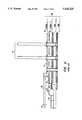
- FIGS. 1-4illustrate, as an example, various views of a conventional plastic pin grid array (“PPGA") package 10.
- the PPGA package 10includes a plastic package body 11 having a cavity area 14 housing an integrated circuit 13.
- the integrated circuit 13is electrically connected to an array of pins 12 extending out of a bottom surface 21 of the package body 11, by bonding wires 15 which connect bond pads 17 formed on the integrated circuit 13 to respective contact fingers 18 formed upon first and second ledge areas, 19 and 20, which in turn, connect through metallic layers 22 to their respective pins 12.
- a ceramic lid 22is attached to the bottom surface 21 of the package body 11 to protect and encase the integrated circuit 13 within the cavity area 14.
- the following aspects of the present inventionare based upon the identification of a number of parasitic noise sources in conventional high performance integrated circuit packages, such as that illustrated in FIGS. 1-4, for example, wherein briefly stated, one such identified source of noise is crosstalk between multiple layers of signal traces (e.g., 23 and 24 in FIG. 2). Uneven current distributions between the pins (e.g., 12) is also identified as another source of noise that is generated when the various signals to the various pins simultaneously switch between logic levels. Still another source of identified noise is induced voltages on the voltage supply and ground lines, which can cause, for example, such phenomena as "ground bounce.”
- one object of the present inventionis to reduce the noise generated in a multi-layered, integrated circuit package by reducing the effects of crosstalk between two or more layers of signal traces.
- Another object of the present inventionis to reduce the noise generated in a high performance integrated circuit package by balancing out the impedance paths formed between the integrated circuit and each of the pins of the integrated circuit package.
- Another object of the present inventionis to reduce the noise generated in a high performance integrated circuit package by reducing the effects of induced voltages along the voltage supply and ground lines.
- Still another general object of the present inventionis to increase both the performance and manufacturability of high performance integrated circuit packages.
- one aspect of the present inventionaccomplishes one or more of these objects by a multi-layered, integrated circuit package structure comprising a plurality of metallic layers formed within the package structure, wherein a metallic layer connected to ground is interposed between first and second metallic layers connected to first and second sets of input/output signals, respectively, so as to inhibit crosstalk between the first and second metallization layers.
- a multi-layered, integrated circuit package structurecomprises a plurality of metallic layers formed within the package structure, wherein a metallic layer connected to input/output signals is sandwiched between a corresponding pair of metallic layers, one of the pair being connected to a voltage supply and the other of the pair being connected to ground, so that the voltage supply and ground metallic layers sandwiching the input/output signal metallic layer inhibit electromagnetic radiation emanating from the input/output signal metallic layer from inducing noise on other circuitry or signal lines within close proximity to the input/output signal metallic layer.
- a multi-layered package structureencases an integrated circuit having a plurality of core transistors for performing a logic function of the integrated circuit, and a plurality of input/output transistors for controlling input/output signals to and from the plurality of core transistors.
- the integrated circuitalso has a plurality of voltage supply bond pads and a plurality of ground bond pads associated with the plurality of core transistors, and a separate plurality of voltage supply bond pads and plurality of ground pads associated with the plurality of input/output transistors.
- the package structurecomprises a plurality of metallization layers including first, second, third, and fourth metallization layers formed on separate planes substantially parallel to one another.
- the first metallization layeris connected to the plurality of voltage supply bond pads associated with the plurality of input/output transistors
- the second metallization layeris connected to the plurality of ground bond pads associated with the plurality of input/output transistors
- the third metallization layeris connected to the plurality of voltage supply bond pads associated with the plurality of core transistors
- the fourth metallization layeris connected to the plurality of ground bond pads associated with the plurality of core transistors.
- a high performance integrated circuit package structurecomprises a two-tiered ledge structure formed around a periphery of a die cavity area, wherein a plurality of contact fingers are formed on both a top tier of the two-tiered structure, and a bottom tier of the two-tiered structure.
- Included among the plurality of contact fingers formed on the top tier of the two-tiered structureare a plurality of ground contact fingers evenly interspersed among a first plurality of input/output signal contact fingers, and included among the plurality of contact fingers formed on the bottom tier of the two-tiered structure are a plurality of voltage supply contact fingers evenly interspersed among a second plurality of input/output signal contact fingers, so as to optimize the current distribution flowing through the first and second plurality of input/output signal contact fingers.
- a high performance integrated circuit package structurecomprises a plurality of pins extending out of a bottom surface of the package structure, wherein associated voltage supply and ground pins are positioned on the bottom surface such that they are substantially the same distance away from a center of an integrated circuit encased in the integrated circuit package structure.
- voltage supply and ground pins corresponding to input/output transistorsare formed in the four outer corners of the bottom surface, and voltage supply and ground pins corresponding to core transistors are formed in four areas, each mid-way between adjacent corners of the four corners.
- FIGS. 1-4illustrate, as examples, a perspective, a partial cross-sectional, a partial bottom plan view without a lid attached over a die cavity area, and a bottom plan view with the lid attached over the die cavity area, respectively, of a conventional plastic pin grid array package ("PPGA");
- PPGAplastic pin grid array package
- FIG. 5illustrates, as an example, a partial cross-sectional view, including a partial die cavity area, two-tiered ledge area, plurality of pins, and plurality of metallization layers useful in connecting an integrated circuit die housed in the die cavity area to the pins, of a PPGA package utilizing aspects of the present invention
- FIGS. 6-7illustrate, as examples, partial cross-sectional views of the PPGA package utilizing aspects of the present invention, showing respectively, first and second signal metallization layers;
- FIG. 8illustrates, as an example, a simplified partial top plan view of an integrated circuit die
- FIG. 9illustrates, as an example, a simplified partial perspective view of a die cavity area and a two-tiered ledge area adjacent to the die cavity area;
- FIG. 10illustrates, as an example, a partial cross-sectional view of the PPGA package utilizing aspects of the present invention, showing a ground metallization layer
- FIG. 11illustrates, as an example, a partially formed, bottom plan view, including a die cavity area, a two-tiered ledge area around a periphery of the die cavity area, and a plurality of contact fingers on each tier of the ledge area of a PPGA package utilizing aspects of the present invention
- FIG. 12illustrates, as an example, a bottom plan view, including a bottom surface and a plurality of pins of a PPGA package utilizing aspects of the present invention.
- FIG. 13illustrates, as an example, a table mapping the contact fingers identified in FIG. 9 to pins identified in FIG. 10.
- FIG. 5illustrates, as an example, a partial, cross-sectional view of a multi-layer, integrated circuit package 100 utilizing aspects of the present invention.
- the integrated circuit package 100houses in a die cavity area 102, an integrated circuit die 104 which is attached, using a silver filled epoxy 106, to a copper plug 108, which acts as both a mechanical support and a heat sink for the integrated circuit die 104.
- the integrated circuit die 104communicates with other electronic devices through package pins 110 which extend out of a bottom surface 112 of the integrated circuit package 100.
- the integrated circuit die 104is electrically connected to the package pins 110 primarily through gold wire bonds 111 and metallization layers 114.
- Each of the gold wire bonds 111is attached at one end to one of a plurality of bond pads 116 (FIG. 11) formed on the integrated circuit die 104, and at another end to a respective one of a plurality of contact fingers, 118 and 120 (FIG. 11), formed on first and second ledges, 122 and 124, respectively, of a two-tiered ledge area adjacent to the die cavity area 102 of the integrated circuit package 100.
- FIGS. 6 and 7illustrate simplified, partial cross-sectional views of the PPGA package utilizing aspects of the present invention, which respectively show first and second input/output signal metallization layers, 202 and 208, formed on insulative layers, 138 and 140, respectively.
- FIG. 6illustrates four contact fingers 118a-118d of the plurality of contact fingers 118 formed on the exposed ledge area 122 of the insulative layer 138
- FIG. 7illustrates three contact fingers 120a-120c of the plurality of contact fingers 120 formed on the exposed ledge area 124 of the insulative layer 140.
- contact rings 128a-128dare respectively formed around plated-through holes 142a-142d
- contact rings 130a-130care respectively formed around plated-through holes 144a-144c.
- Each of the plated-through holes, e.g., 142a-142d and 144a-144c,holds a respective one of the package pins 110
- each of the contact rings, e.g., 128a-128d and 130a-130cmakes electrical contact with a pin being held by its respective plated-through hole.
- contact fingers 118a-118d, conductive traces 126a-126d, and contact rings 128a-128dare concurrently formed together as metallization layer 202 on insulative layer 138, and contact fingers 120a-120c, conductive traces 132a-132c, and contact rings 130a-130c are concurrently formed together as metallization layer 208 on insulative layer 140, using conventional metallization techniques.
- the integrated circuit die 104has a top surface 500 having a core area 300 and an input/output area 400.
- a plurality of transistorse.g., 302-304
- Formed in the core area 300are a plurality of transistors (e.g., 302-304) which perform the basic logic functions of the integrated circuit die 104.
- Formed in the input/output area 400are a plurality of bond pads 116, and a plurality of input/output transistors (e.g., 402-403) which control the transmission and reception of input/output signals from and to the core transistors (e.g., 302-304), and to and from respective bond pads 116 on the integrated circuit die 104.
- the connection of the bond pads 116 to their respective package pinshas already been described.
- Voltage supply and ground inputs(e.g., VDD CORE and VSS CORE) provided to the core transistors (e.g., 302-304) are separated from voltage supply and ground inputs (e.g., VDD I/O and VSS I/O) provided to the input/output transistors (e.g., 402-403).
- the separated voltage supply and ground inputs(e.g., VDD CORE, VDD I/O, VSS CORE, and VSS I/O) are connected through selected ones of the package pins 110 to respective contact fingers and thence, to respective bond pads on the integrated circuit die 104, through separate metallization layers (e.g., 206, 200, 210, and 204, respectively).
- the core transistorse.g., 302-304
- Another reason for such separationis to allow the core and input/output transistors to operate from different supply voltages.
- the core transistorse.g., 302-304
- the input/output transistorse.g., 402-403
- the ordering of the metallization layers 114is selected such that parasitic noise generated, for example, by crosstalk between signal metallization layers, is minimized.
- the input/output ground metallization layer 204e.g., VSS I/O
- VSS I/Oinput/output ground metallization layer
- each signal metallization layeris sandwiched in between a voltage supply and ground pair to further inhibit induced noise being generated in other parts of the circuitry due to simultaneous switching of the input/output transistors connected to respective conductive traces in that metallization layer.
- the first signal metallization layer 202is sandwiched in between input/output voltage supply (e.g., VDD I/O) and input/output ground (e.g., VSS I/O) metallization layers, 200 and 204, respectively, and the second signal metallization layer 208 is sandwiched in between core voltage supply (e.g., VDD CORE) and core ground (e.g., VSS CORE) metallization layers, 206 and 210, respectively.
- input/output voltage supplye.g., VDD I/O
- input/output grounde.g., VSS I/O
- core voltage supplye.g., VDD CORE
- core grounde.g., VSS CORE
- the voltage supply and ground metallization layers, 200, 204, 206, and 210are on separate planes (i.e., layers) than their respective contact fingers, conventional contact holes or vias may be formed through the insulating layers, 138 and 140, where appropriate, to connect the voltage supply and ground metallization layers, 200, 204, 206, and 210, to their respective contact fingers.
- an alternative techniqueis employed for at least the ground metallization layers, 204 and 210.
- FIG. 9illustrates, as an example, a simplified partial perspective view of the cavity area 102 including the copper slug 108, and the two-tiered ledge area including ledges 122 and 124.
- a VSS I/O contact finger 120dconnects to the VSS I/O ground metallization layer 204 through a conductive trace 146 formed on the exterior wall 136 of the second ledge area 124
- VSS CORE contact finger 118econnects to the VSS CORE ground metallization layer 210 through a conductive trace 148 formed on the exterior wall 134 of the first ledge area 122.
- conductive traces, 146 and 148By forming such conductive traces, 146 and 148, over the exterior ledge walls, 136 and 134, respectively, the necessity to form contact holes or vias to accomplish the same result is eliminated.
- another conductive trace 150is formed on the exterior wall 134 of the first ledge area 122, which extends from the VSS CORE ground metallization layer 210 directly to the copper slug 108.
- this contact area of the VSS CORE ground lineis further isolated from the noisy conductive traces (e.g., 126a-126d and 132a-132c) and consequently, also serves to reduce the parasitic noise induced upon the VSS CORE ground line by these conductive traces (e.g., 126a-126d and 132a-132c).
- FIG. 10illustrates, as an example, a simplified, partial cross-sectional view of the PPGA package utilizing aspects of the present invention, which shows the VSS I/O metallization layer 204 formed on a plane (i.e., layer) between the ledge areas 122 and 124 formed on insulative layers 138 and 140, respectively.
- a wide contact area 160extending to the exterior wall 136 and connecting, through conductive trace 156, to contact ring 152 which holds the one pin, can be provided.
- VSS I/O contact fingerscan also be connected to another pin through a similar contact area 162 extending to the exterior wall 136 and connecting, through conductive trace 158, to contact ring 154 which holds the other pin. Although it is possible to connect contact areas 160 and 162 together, isolation of these areas, as illustrated, further serves to reduce parasitic noise generated on these lines through induction from the input/output signals and other noise generating sources.
- VSS CORE, VDD I/O, and VDD CORE metallization layers 210, 200, and 206, respectively,may be similarly formed.
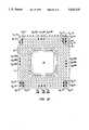
- FIG. 11illustrates, as an example, a partially formed, bottom plan view, including a die cavity area 102, a two-tiered ledge area formed around a periphery of the die cavity area 102, and a plurality of contact fingers, 118 and 120, on each tier, 122 and 124, respectively, of the ledge area of a PPGA package 100 utilizing aspects of the present invention.
- a plurality of input/output signal contact fingersare shown as being evenly interspersed among a plurality of VSS I/O contact fingers.
- the number of input/output signal contact fingers formed between adjacent VSS I/O contact fingersis shown to be either 3 or 4 contact fingers.
- parasitic noise induced by crosstalkcan be reduced between input/output signal contact fingers, and the current distribution to the input/output signal package pins can be shown to be more evenly distributed.
- ground bouncei.e., a moving ground reference line
- a second plurality of input/output signal contact fingersare shown as being evenly interspersed among a plurality of VDD I/O contact fingers on the first ledge area 122.
- the number of input/output signal contact fingers formed between adjacent VDD I/O contact fingersis shown to be generally 6 to 8 contact fingers.
- VSS CORE and VDD CORE contact fingersare also formed on the first ledge area 122.
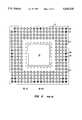
- FIG. 12illustrates, as an example, a bottom plan view, including a bottom surface 112 and a plurality of pins 110 extending out of the bottom surface 112 of the PPGA package 100 utilizing aspects of the present invention
- FIG. 13illustrates, as an example, a table mapping the input/output signal contact fingers identified in FIG. 11 by pad numbers (e.g., pad number 1), to their respective package pins as identified in FIG. 12 by pin numbers (e.g., pin number D4).
- pad numberse.g., pad number 1
- pin numberse.g., pin number D4
- VDD CORE and VSS CORE pinsare shown in FIG. 12 to be placed in four areas, each area mid-way between adjacent corners of the bottom surface 112.
- pins A17 and B18are identified as VDD I/O pins
- pins A18 and B17are identified as VSS I/O pins
- pins J18 and L18are identified as VSS CORE pins
- pin K18is identified as a VDD CORE pin.
- the parasitic noise induced on these lines from the switching of active circuitry on the integrated circuit die 104can be shown to be evenly distributed and as a consequence, "ground bounce" is reduced.
- the parasitic noise induced on these linescan also be shown to be evenly distributed with similar benefits.
- VSS pins 28 and 26which are connected together through a common VSS metallic layer (FIG. 2), are not a same distance from a center of the integrated circuit 13 housed under ceramic lid 22.
- VSS pin 28, which is formed in a corner of the bottom surface 21 of the package structure 10is clearly further away from the center of the integrated circuit 13 than VSS pin 26, which is formed in an area mid-way between adjacent corners of the package structure 10.
- two chip capacitor padse.g., 601 and 602, adjacent to the VDD I/O and VSS I/O pins in the upper right hand corner of the figure, are also shown.
- One of the padse.g., 601 is connected to the VDD I/O pins, and the other of the pads (e.g., 602) is connected to the VSS I/O pins in the upper right hand corner.
Landscapes
- Physics & Mathematics (AREA)
- Engineering & Computer Science (AREA)
- Computer Hardware Design (AREA)
- Microelectronics & Electronic Packaging (AREA)
- Power Engineering (AREA)
- Condensed Matter Physics & Semiconductors (AREA)
- General Physics & Mathematics (AREA)
- Geometry (AREA)
- Semiconductor Integrated Circuits (AREA)
Abstract
Description
Claims (2)
Priority Applications (1)
| Application Number | Priority Date | Filing Date | Title |
|---|---|---|---|
| US08/589,751US5625225A (en) | 1993-12-22 | 1996-01-22 | Multi-layered, integrated circuit package having reduced parasitic noise characteristics |
Applications Claiming Priority (2)
| Application Number | Priority Date | Filing Date | Title |
|---|---|---|---|
| US17250293A | 1993-12-22 | 1993-12-22 | |
| US08/589,751US5625225A (en) | 1993-12-22 | 1996-01-22 | Multi-layered, integrated circuit package having reduced parasitic noise characteristics |
Related Parent Applications (1)
| Application Number | Title | Priority Date | Filing Date |
|---|---|---|---|
| US17250293AContinuation | 1993-12-22 | 1993-12-22 |
Publications (1)
| Publication Number | Publication Date |
|---|---|
| US5625225Atrue US5625225A (en) | 1997-04-29 |
Family
ID=22627968
Family Applications (2)
| Application Number | Title | Priority Date | Filing Date |
|---|---|---|---|
| US08/549,985Expired - LifetimeUS5641988A (en) | 1993-12-22 | 1995-10-30 | Multi-layered, integrated circuit package having reduced parasitic noise characteristics |
| US08/589,751Expired - LifetimeUS5625225A (en) | 1993-12-22 | 1996-01-22 | Multi-layered, integrated circuit package having reduced parasitic noise characteristics |
Family Applications Before (1)
| Application Number | Title | Priority Date | Filing Date |
|---|---|---|---|
| US08/549,985Expired - LifetimeUS5641988A (en) | 1993-12-22 | 1995-10-30 | Multi-layered, integrated circuit package having reduced parasitic noise characteristics |
Country Status (1)
| Country | Link |
|---|---|
| US (2) | US5641988A (en) |
Cited By (21)
| Publication number | Priority date | Publication date | Assignee | Title |
|---|---|---|---|---|
| WO1998010466A1 (en)* | 1996-09-09 | 1998-03-12 | Intel Corporation | An integrated circuit package |
| US5787575A (en)* | 1996-09-09 | 1998-08-04 | Intel Corporation | Method for plating a bond finger of an intergrated circuit package |
| WO1999029594A1 (en)* | 1997-12-08 | 1999-06-17 | Koh Lawrence R | Self-ejecting compact disc case |
| US5981880A (en)* | 1996-08-20 | 1999-11-09 | International Business Machines Corporation | Electronic device packages having glass free non conductive layers |
| US6025616A (en)* | 1997-06-25 | 2000-02-15 | Honeywell Inc. | Power distribution system for semiconductor die |
| US6054758A (en)* | 1996-12-18 | 2000-04-25 | Texas Instruments Incorporated | Differential pair geometry for integrated circuit chip packages |
| US6181004B1 (en)* | 1999-01-22 | 2001-01-30 | Jerry D. Koontz | Digital signal processing assembly and test method |
| US6225690B1 (en)* | 1999-12-10 | 2001-05-01 | Lsi Logic Corporation | Plastic ball grid array package with strip line configuration |
| US6429051B1 (en) | 2000-12-29 | 2002-08-06 | Intel Corporation | Stitched plane structure for package power delivery and dual referenced stripline I/O performance |
| US6438830B1 (en)* | 1997-04-16 | 2002-08-27 | International Business Machines Corporation | Process of producing plastic pin grid array |
| US7442083B1 (en)* | 2007-07-20 | 2008-10-28 | Lotes Co., Ltd. | Electrical connector |
| US20090039498A1 (en)* | 2007-08-06 | 2009-02-12 | Infineon Technologies Ag | Power semiconductor module |
| US20100065962A1 (en)* | 2007-08-06 | 2010-03-18 | Infineon Technologies Ag | Power semiconductor module |
| US8547677B2 (en) | 2005-03-01 | 2013-10-01 | X2Y Attenuators, Llc | Method for making internally overlapped conditioners |
| US8587915B2 (en) | 1997-04-08 | 2013-11-19 | X2Y Attenuators, Llc | Arrangement for energy conditioning |
| US9036319B2 (en) | 1997-04-08 | 2015-05-19 | X2Y Attenuators, Llc | Arrangement for energy conditioning |
| US9054094B2 (en) | 1997-04-08 | 2015-06-09 | X2Y Attenuators, Llc | Energy conditioning circuit arrangement for integrated circuit |
| US20150228602A1 (en)* | 2014-02-12 | 2015-08-13 | Sony Corporation | Semicondcutor chip and semionducot module |
| WO2015164095A3 (en)* | 2014-04-21 | 2016-12-08 | Henkel IP & Holding GmbH | Curable adhesive compositions and use thereof |
| US20170243802A1 (en)* | 2006-04-27 | 2017-08-24 | International Business Machines Corporation | Integrated circuit chip packaging |
| US10808072B2 (en) | 2014-04-21 | 2020-10-20 | Henkel IP & Holding GmbH | Curable adhesive compositions and use thereof |
Families Citing this family (6)
| Publication number | Priority date | Publication date | Assignee | Title |
|---|---|---|---|---|
| US5654204A (en)* | 1994-07-20 | 1997-08-05 | Anderson; James C. | Die sorter |
| JP3362545B2 (en)* | 1995-03-09 | 2003-01-07 | ソニー株式会社 | Method for manufacturing semiconductor device |
| WO2004100260A1 (en)* | 1995-05-19 | 2004-11-18 | Kouta Noda | High-density multi-layered printed wiring board, multi-chip carrier, and semiconductor package |
| JPH1174407A (en)* | 1997-08-29 | 1999-03-16 | Mitsubishi Electric Corp | Semiconductor device |
| US6129613A (en)* | 1998-01-30 | 2000-10-10 | Philips Electronics North America Corp. | Semiconductor manufacturing apparatus and method for measuring in-situ pressure across a wafer |
| US6057596A (en)* | 1998-10-19 | 2000-05-02 | Silicon Integrated Systems Corp. | Chip carrier having a specific power join distribution structure |
Citations (7)
| Publication number | Priority date | Publication date | Assignee | Title |
|---|---|---|---|---|
| US4675789A (en)* | 1984-12-28 | 1987-06-23 | Fujitsu Limited | High density multilayer printed circuit board |
| US4884170A (en)* | 1982-04-16 | 1989-11-28 | Hitachi, Ltd. | Multilayer printed circuit board and method of producing the same |
| US4972253A (en)* | 1988-06-27 | 1990-11-20 | Digital Equipment Corporation | Programmable ceramic high performance custom package |
| JPH04184962A (en)* | 1990-11-20 | 1992-07-01 | Hitachi Ltd | Semiconductor integrated circuit device |
| US5363280A (en)* | 1993-04-22 | 1994-11-08 | International Business Machines Corporation | Printed circuit board or card thermal mass design |
| US5365406A (en)* | 1991-02-01 | 1994-11-15 | Nec Corporation | Master-slice type semiconductor integrated circuit device |
| US5365091A (en)* | 1992-06-11 | 1994-11-15 | Hitachi, Ltd. | Semiconductor integrated circuit device |
Family Cites Families (2)
| Publication number | Priority date | Publication date | Assignee | Title |
|---|---|---|---|---|
| EP0459179B1 (en)* | 1990-05-28 | 1995-04-05 | Siemens Aktiengesellschaft | IC-housing made of three coated dielectric plates |
| US5220489A (en)* | 1991-10-11 | 1993-06-15 | Motorola, Inc. | Multicomponent integrated circuit package |
- 1995
- 1995-10-30USUS08/549,985patent/US5641988A/ennot_activeExpired - Lifetime
- 1996
- 1996-01-22USUS08/589,751patent/US5625225A/ennot_activeExpired - Lifetime
Patent Citations (7)
| Publication number | Priority date | Publication date | Assignee | Title |
|---|---|---|---|---|
| US4884170A (en)* | 1982-04-16 | 1989-11-28 | Hitachi, Ltd. | Multilayer printed circuit board and method of producing the same |
| US4675789A (en)* | 1984-12-28 | 1987-06-23 | Fujitsu Limited | High density multilayer printed circuit board |
| US4972253A (en)* | 1988-06-27 | 1990-11-20 | Digital Equipment Corporation | Programmable ceramic high performance custom package |
| JPH04184962A (en)* | 1990-11-20 | 1992-07-01 | Hitachi Ltd | Semiconductor integrated circuit device |
| US5365406A (en)* | 1991-02-01 | 1994-11-15 | Nec Corporation | Master-slice type semiconductor integrated circuit device |
| US5365091A (en)* | 1992-06-11 | 1994-11-15 | Hitachi, Ltd. | Semiconductor integrated circuit device |
| US5363280A (en)* | 1993-04-22 | 1994-11-08 | International Business Machines Corporation | Printed circuit board or card thermal mass design |
Non-Patent Citations (2)
| Title |
|---|
| "Low Inductance Multilayer Ceramic Module", IBM Tech. Disc. Bulletin, vol. 32, No. 10B; pp. 256-258, Mar., 1990. |
| Low Inductance Multilayer Ceramic Module , IBM Tech. Disc. Bulletin, vol. 32, No. 10B; pp. 256 258, Mar., 1990.* |
Cited By (37)
| Publication number | Priority date | Publication date | Assignee | Title |
|---|---|---|---|---|
| US5981880A (en)* | 1996-08-20 | 1999-11-09 | International Business Machines Corporation | Electronic device packages having glass free non conductive layers |
| US6781064B1 (en) | 1996-08-20 | 2004-08-24 | International Business Machines Corporation | Printed circuit boards for electronic device packages having glass free non-conductive layers and method of forming same |
| GB2333182B (en)* | 1996-09-09 | 2001-08-15 | Intel Corp | An integrated circuit package |
| US5787575A (en)* | 1996-09-09 | 1998-08-04 | Intel Corporation | Method for plating a bond finger of an intergrated circuit package |
| KR100488324B1 (en)* | 1996-09-09 | 2005-05-10 | 인텔 코오퍼레이션 | an integrated circuit package |
| GB2333182A (en)* | 1996-09-09 | 1999-07-14 | Intel Corp | An integrated circuit package |
| US6031283A (en)* | 1996-09-09 | 2000-02-29 | Intel Corporation | Integrated circuit package |
| WO1998010466A1 (en)* | 1996-09-09 | 1998-03-12 | Intel Corporation | An integrated circuit package |
| US6054758A (en)* | 1996-12-18 | 2000-04-25 | Texas Instruments Incorporated | Differential pair geometry for integrated circuit chip packages |
| US6323116B1 (en)* | 1996-12-18 | 2001-11-27 | Texas Instruments Incorporated | Differential pair geometry for integrated circuit chip packages |
| US9373592B2 (en) | 1997-04-08 | 2016-06-21 | X2Y Attenuators, Llc | Arrangement for energy conditioning |
| US8587915B2 (en) | 1997-04-08 | 2013-11-19 | X2Y Attenuators, Llc | Arrangement for energy conditioning |
| US9054094B2 (en) | 1997-04-08 | 2015-06-09 | X2Y Attenuators, Llc | Energy conditioning circuit arrangement for integrated circuit |
| US9036319B2 (en) | 1997-04-08 | 2015-05-19 | X2Y Attenuators, Llc | Arrangement for energy conditioning |
| US9019679B2 (en) | 1997-04-08 | 2015-04-28 | X2Y Attenuators, Llc | Arrangement for energy conditioning |
| US6438830B1 (en)* | 1997-04-16 | 2002-08-27 | International Business Machines Corporation | Process of producing plastic pin grid array |
| US6025616A (en)* | 1997-06-25 | 2000-02-15 | Honeywell Inc. | Power distribution system for semiconductor die |
| WO1999029594A1 (en)* | 1997-12-08 | 1999-06-17 | Koh Lawrence R | Self-ejecting compact disc case |
| US6181004B1 (en)* | 1999-01-22 | 2001-01-30 | Jerry D. Koontz | Digital signal processing assembly and test method |
| US6225690B1 (en)* | 1999-12-10 | 2001-05-01 | Lsi Logic Corporation | Plastic ball grid array package with strip line configuration |
| US6429051B1 (en) | 2000-12-29 | 2002-08-06 | Intel Corporation | Stitched plane structure for package power delivery and dual referenced stripline I/O performance |
| US6501166B2 (en)* | 2000-12-29 | 2002-12-31 | Intel Corporation | Stitched plane structure and process for package power delivery and dual referenced stripline I/O performance |
| US9001486B2 (en) | 2005-03-01 | 2015-04-07 | X2Y Attenuators, Llc | Internally overlapped conditioners |
| US8547677B2 (en) | 2005-03-01 | 2013-10-01 | X2Y Attenuators, Llc | Method for making internally overlapped conditioners |
| US20170243816A1 (en)* | 2006-04-27 | 2017-08-24 | International Business Machines Corporation | Integrated circuit chip packaging |
| US20170243802A1 (en)* | 2006-04-27 | 2017-08-24 | International Business Machines Corporation | Integrated circuit chip packaging |
| US10600715B2 (en)* | 2006-04-27 | 2020-03-24 | International Business Machines Corporation | Integrated circuit chip packaging |
| US10818572B2 (en)* | 2006-04-27 | 2020-10-27 | International Business Machines Corporation | Integrated circuit chip packaging including a heat sink topped cavity |
| US7442083B1 (en)* | 2007-07-20 | 2008-10-28 | Lotes Co., Ltd. | Electrical connector |
| US20090039498A1 (en)* | 2007-08-06 | 2009-02-12 | Infineon Technologies Ag | Power semiconductor module |
| US20100065962A1 (en)* | 2007-08-06 | 2010-03-18 | Infineon Technologies Ag | Power semiconductor module |
| US8154114B2 (en) | 2007-08-06 | 2012-04-10 | Infineon Technologies Ag | Power semiconductor module |
| US8018047B2 (en)* | 2007-08-06 | 2011-09-13 | Infineon Technologies Ag | Power semiconductor module including a multilayer substrate |
| US20150228602A1 (en)* | 2014-02-12 | 2015-08-13 | Sony Corporation | Semicondcutor chip and semionducot module |
| WO2015164095A3 (en)* | 2014-04-21 | 2016-12-08 | Henkel IP & Holding GmbH | Curable adhesive compositions and use thereof |
| US10808072B2 (en) | 2014-04-21 | 2020-10-20 | Henkel IP & Holding GmbH | Curable adhesive compositions and use thereof |
| US11505645B2 (en) | 2014-04-21 | 2022-11-22 | Henkel Ag & Co., Kgaa | Curable adhesive compositions and use thereof |
Also Published As
| Publication number | Publication date |
|---|---|
| US5641988A (en) | 1997-06-24 |
Similar Documents
| Publication | Publication Date | Title |
|---|---|---|
| US5625225A (en) | Multi-layered, integrated circuit package having reduced parasitic noise characteristics | |
| US5686764A (en) | Flip chip package with reduced number of package layers | |
| US4972253A (en) | Programmable ceramic high performance custom package | |
| US4577214A (en) | Low-inductance power/ground distribution in a package for a semiconductor chip | |
| US5283717A (en) | Circuit assembly having interposer lead frame | |
| US5426566A (en) | Multichip integrated circuit packages and systems | |
| US5701233A (en) | Stackable modules and multimodular assemblies | |
| US4744008A (en) | Flexible film chip carrier with decoupling capacitors | |
| JP3758678B2 (en) | High performance integrated circuit package | |
| US7098542B1 (en) | Multi-chip configuration to connect flip-chips to flip-chips | |
| US4887148A (en) | Pin grid array package structure | |
| JP4597512B2 (en) | Single package including multiple integrated circuit devices and method for packaging semiconductor devices | |
| US8536713B2 (en) | System in package with heat sink | |
| EP0268260B1 (en) | Flexible film chip carrier with decoupling capacitors | |
| KR100299560B1 (en) | High density integrated circuit assembly combining lead frame leads and conductive traces | |
| US6114903A (en) | Layout architecture for core I/O buffer | |
| US5399904A (en) | Array type semiconductor device having insulating circuit board | |
| WO1996008841A1 (en) | A high density integrated circuit assembly combining leadframe leads with conductive traces | |
| US5650660A (en) | Circuit pattern for a ball grid array integrated circuit package | |
| US5914533A (en) | Multilayer module with thinfilm redistribution area | |
| US6307259B1 (en) | Plastic package for semiconductor device | |
| Darnauer et al. | A field programmable multi-chip module (FPMCM) | |
| EP0077818B1 (en) | A pacakage for a semiconductor chip having a capacitor as an integral part thereof | |
| JPS6256664B2 (en) | ||
| JPH0519983B2 (en) |
Legal Events
| Date | Code | Title | Description |
|---|---|---|---|
| STCF | Information on status: patent grant | Free format text:PATENTED CASE | |
| FEPP | Fee payment procedure | Free format text:PAYOR NUMBER ASSIGNED (ORIGINAL EVENT CODE: ASPN); ENTITY STATUS OF PATENT OWNER: LARGE ENTITY | |
| FPAY | Fee payment | Year of fee payment:4 | |
| FPAY | Fee payment | Year of fee payment:8 | |
| FPAY | Fee payment | Year of fee payment:12 | |
| AS | Assignment | Owner name:TAIWAN SEMICONDUCTOR MANUFACTURING COMPANY, LTD., Free format text:ASSIGNMENT OF ASSIGNORS INTEREST;ASSIGNOR:NXP B.V.;REEL/FRAME:022266/0047 Effective date:20090217 Owner name:TAIWAN SEMICONDUCTOR MANUFACTURING COMPANY, LTD.,T Free format text:ASSIGNMENT OF ASSIGNORS INTEREST;ASSIGNOR:NXP B.V.;REEL/FRAME:022266/0047 Effective date:20090217 | |
| AS | Assignment | Owner name:NXP B.V., NETHERLANDS Free format text:ASSIGNMENT OF ASSIGNORS INTEREST;ASSIGNOR:PHILIPS SEMICONDUCTORS INC.;REEL/FRAME:022973/0239 Effective date:20090715 Owner name:PHILIPS SEMICONDUCTORS VLSI INC., NEW YORK Free format text:CHANGE OF NAME;ASSIGNOR:VLSI TECHNOLOGY, INC.;REEL/FRAME:022973/0248 Effective date:19990702 Owner name:PHILIPS SEMICONDUCTORS INC., NEW YORK Free format text:CHANGE OF NAME;ASSIGNOR:PHILIPS SEMICONDUCTORS VLSI INC.;REEL/FRAME:022973/0254 Effective date:19991229 |