US5625221A - Semiconductor assembly for a three-dimensional integrated circuit package - Google Patents
Semiconductor assembly for a three-dimensional integrated circuit packageDownload PDFInfo
- Publication number
- US5625221A US5625221AUS08/368,165US36816595AUS5625221AUS 5625221 AUS5625221 AUS 5625221AUS 36816595 AUS36816595 AUS 36816595AUS 5625221 AUS5625221 AUS 5625221A
- Authority
- US
- United States
- Prior art keywords
- semiconductor chip
- chip package
- lead
- leads
- assembly
- Prior art date
- Legal status (The legal status is an assumption and is not a legal conclusion. Google has not performed a legal analysis and makes no representation as to the accuracy of the status listed.)
- Expired - Lifetime
Links
Images


Classifications
- D—TEXTILES; PAPER
- D06—TREATMENT OF TEXTILES OR THE LIKE; LAUNDERING; FLEXIBLE MATERIALS NOT OTHERWISE PROVIDED FOR
- D06B—TREATING TEXTILE MATERIALS USING LIQUIDS, GASES OR VAPOURS
- D06B3/00—Passing of textile materials through liquids, gases or vapours to effect treatment, e.g. washing, dyeing, bleaching, sizing, impregnating
- D06B3/32—Passing of textile materials through liquids, gases or vapours to effect treatment, e.g. washing, dyeing, bleaching, sizing, impregnating of open-width materials backwards and forwards between beaming rollers during treatment; Jiggers
- H—ELECTRICITY
- H01—ELECTRIC ELEMENTS
- H01L—SEMICONDUCTOR DEVICES NOT COVERED BY CLASS H10
- H01L25/00—Assemblies consisting of a plurality of semiconductor or other solid state devices
- H01L25/03—Assemblies consisting of a plurality of semiconductor or other solid state devices all the devices being of a type provided for in a single subclass of subclasses H10B, H10D, H10F, H10H, H10K or H10N, e.g. assemblies of rectifier diodes
- H01L25/10—Assemblies consisting of a plurality of semiconductor or other solid state devices all the devices being of a type provided for in a single subclass of subclasses H10B, H10D, H10F, H10H, H10K or H10N, e.g. assemblies of rectifier diodes the devices having separate containers
- H01L25/105—Assemblies consisting of a plurality of semiconductor or other solid state devices all the devices being of a type provided for in a single subclass of subclasses H10B, H10D, H10F, H10H, H10K or H10N, e.g. assemblies of rectifier diodes the devices having separate containers the devices being integrated devices of class H10
- D—TEXTILES; PAPER
- D06—TREATMENT OF TEXTILES OR THE LIKE; LAUNDERING; FLEXIBLE MATERIALS NOT OTHERWISE PROVIDED FOR
- D06B—TREATING TEXTILE MATERIALS USING LIQUIDS, GASES OR VAPOURS
- D06B23/00—Component parts, details, or accessories of apparatus or machines, specially adapted for the treating of textile materials, not restricted to a particular kind of apparatus, provided for in groups D06B1/00 - D06B21/00
- D06B23/02—Rollers
- D06B23/023—Guiding rollers
- D—TEXTILES; PAPER
- D06—TREATMENT OF TEXTILES OR THE LIKE; LAUNDERING; FLEXIBLE MATERIALS NOT OTHERWISE PROVIDED FOR
- D06B—TREATING TEXTILE MATERIALS USING LIQUIDS, GASES OR VAPOURS
- D06B23/00—Component parts, details, or accessories of apparatus or machines, specially adapted for the treating of textile materials, not restricted to a particular kind of apparatus, provided for in groups D06B1/00 - D06B21/00
- D06B23/04—Carriers or supports for textile materials to be treated
- H—ELECTRICITY
- H01—ELECTRIC ELEMENTS
- H01L—SEMICONDUCTOR DEVICES NOT COVERED BY CLASS H10
- H01L2224/00—Indexing scheme for arrangements for connecting or disconnecting semiconductor or solid-state bodies and methods related thereto as covered by H01L24/00
- H01L2224/01—Means for bonding being attached to, or being formed on, the surface to be connected, e.g. chip-to-package, die-attach, "first-level" interconnects; Manufacturing methods related thereto
- H01L2224/42—Wire connectors; Manufacturing methods related thereto
- H01L2224/47—Structure, shape, material or disposition of the wire connectors after the connecting process
- H01L2224/48—Structure, shape, material or disposition of the wire connectors after the connecting process of an individual wire connector
- H01L2224/4805—Shape
- H01L2224/4809—Loop shape
- H01L2224/48091—Arched
- H—ELECTRICITY
- H01—ELECTRIC ELEMENTS
- H01L—SEMICONDUCTOR DEVICES NOT COVERED BY CLASS H10
- H01L2224/00—Indexing scheme for arrangements for connecting or disconnecting semiconductor or solid-state bodies and methods related thereto as covered by H01L24/00
- H01L2224/01—Means for bonding being attached to, or being formed on, the surface to be connected, e.g. chip-to-package, die-attach, "first-level" interconnects; Manufacturing methods related thereto
- H01L2224/42—Wire connectors; Manufacturing methods related thereto
- H01L2224/47—Structure, shape, material or disposition of the wire connectors after the connecting process
- H01L2224/48—Structure, shape, material or disposition of the wire connectors after the connecting process of an individual wire connector
- H01L2224/481—Disposition
- H01L2224/48151—Connecting between a semiconductor or solid-state body and an item not being a semiconductor or solid-state body, e.g. chip-to-substrate, chip-to-passive
- H01L2224/48221—Connecting between a semiconductor or solid-state body and an item not being a semiconductor or solid-state body, e.g. chip-to-substrate, chip-to-passive the body and the item being stacked
- H01L2224/48245—Connecting between a semiconductor or solid-state body and an item not being a semiconductor or solid-state body, e.g. chip-to-substrate, chip-to-passive the body and the item being stacked the item being metallic
- H01L2224/48247—Connecting between a semiconductor or solid-state body and an item not being a semiconductor or solid-state body, e.g. chip-to-substrate, chip-to-passive the body and the item being stacked the item being metallic connecting the wire to a bond pad of the item
- H—ELECTRICITY
- H01—ELECTRIC ELEMENTS
- H01L—SEMICONDUCTOR DEVICES NOT COVERED BY CLASS H10
- H01L2225/00—Details relating to assemblies covered by the group H01L25/00 but not provided for in its subgroups
- H01L2225/03—All the devices being of a type provided for in the same main group of the same subclass of class H10, e.g. assemblies of rectifier diodes
- H01L2225/10—All the devices being of a type provided for in the same main group of the same subclass of class H10, e.g. assemblies of rectifier diodes the devices having separate containers
- H01L2225/1005—All the devices being of a type provided for in the same main group of the same subclass of class H10, e.g. assemblies of rectifier diodes the devices having separate containers the devices being integrated devices of class H10
- H01L2225/1011—All the devices being of a type provided for in the same main group of the same subclass of class H10, e.g. assemblies of rectifier diodes the devices having separate containers the devices being integrated devices of class H10 the containers being in a stacked arrangement
- H01L2225/1017—All the devices being of a type provided for in the same main group of the same subclass of class H10, e.g. assemblies of rectifier diodes the devices having separate containers the devices being integrated devices of class H10 the containers being in a stacked arrangement the lowermost container comprising a device support
- H01L2225/1029—All the devices being of a type provided for in the same main group of the same subclass of class H10, e.g. assemblies of rectifier diodes the devices having separate containers the devices being integrated devices of class H10 the containers being in a stacked arrangement the lowermost container comprising a device support the support being a lead frame
- H—ELECTRICITY
- H01—ELECTRIC ELEMENTS
- H01L—SEMICONDUCTOR DEVICES NOT COVERED BY CLASS H10
- H01L2924/00—Indexing scheme for arrangements or methods for connecting or disconnecting semiconductor or solid-state bodies as covered by H01L24/00
- H01L2924/15—Details of package parts other than the semiconductor or other solid state devices to be connected
- H01L2924/151—Die mounting substrate
- H01L2924/153—Connection portion
- H01L2924/1532—Connection portion the connection portion being formed on the die mounting surface of the substrate
- H—ELECTRICITY
- H01—ELECTRIC ELEMENTS
- H01L—SEMICONDUCTOR DEVICES NOT COVERED BY CLASS H10
- H01L2924/00—Indexing scheme for arrangements or methods for connecting or disconnecting semiconductor or solid-state bodies as covered by H01L24/00
- H01L2924/19—Details of hybrid assemblies other than the semiconductor or other solid state devices to be connected
- H01L2924/1901—Structure
- H01L2924/1904—Component type
- H01L2924/19041—Component type being a capacitor
Definitions
- the present inventionrelates to a semiconductor assembly for an improved three-dimensional integrated circuit structure, and more particularly, to a semiconductor assembly having a stacked module structure employing a heat sink and a capacitor plate.
- Three-dimensional packaging technologyhas become useful in electronic systems needing larger capacity, faster operating speed, and minimized size.
- Previously proposed three-dimensional packaging technologiesinclude chip-stacked type and assembly-stacked type. Almost all assembly manufacturers utilize configurations for reducing device size in order to enhance operating speed and to increase capacity.
- the chip-stacked packagewhen implemented, has low reliability, high cost, and a long developing period.
- the assembly-stacked packagestill has disadvantages compared with a two-dimensional packaging configuration. It requires process steps for vertical interconnection in addition to the basic packaging process for a semiconductor assembly. It also requires mounting a heat sink on each semiconductor assembly using an additional process step, or employing a separate cooling device for heat emission. Each heat sink on each assembly increases the volume of the stacked package when implemented and also makes high density packaging impossible. If the cooling device is employed, the cost for manufacturing the assembly-stacked package is increased.
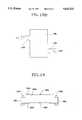
- FIG. 1illustrates a conventional assembly-stacked package disclosed in an article titled "3-D Stacked Memory Devices Using a Proprietary Process" proposed by STAKTEK CO.
- Leads 12 protruding from assemblies 11are electrically connected to a connecter 13 after the assemblies 11 have been stacked atop each other. Then, for heat emission, thin metal foil portions are stacked between the assemblies 11, or, as shown in FIG. 1., a grounded heat sink 14 is formed to cover the overall stacked structure.
- FIG. 1the packaging configuration of FIG. 1 is a difficult to use with further structures with a core as a carrier for interconnecting between the assemblies 11. Also, this configuration is not well-suited to mass-production since it is not generally compatible used with existing manufacturing apparatuses.
- the leads 22are inserted into pin holes 26 on two printed circuit boards 23 that are inserted into connection sockets 25.
- the folded leads 22, as shown in FIG. 2B,extend through the pin holes 26 and are attached to the printed circuit boards 23 by solder 24.
- the disclosed devicehowever, has several topological limitations such that it is difficult to increase the packing density due the height of the device. It is also difficult to increase the number of the assemblies which can be stacked therein.
- the attaching portions between the assemblies and the printed circuit boardsare connected only by the bonding force of the solder, which can be structurally weak.
- a single in-line memory module developed by RTB Co.includes a plurality of assemblies 31, each having a plurality of leads 32.
- Each lead 32has a pin hole connecting the lead 32 to a corresponding vertical lead 36.
- a plurality of pins 35extend between a bottom plate 34 and a top plate 33 and pass through the pin holes of leads 32, so that the leads 32 are fixed thereto and supported by the pins 35.
- the top plate 33has a plurality of grooves (not shown) to engage the pins 35, which also protrude under the bottom plate 34 for mounting on a printing circuit board (not shown). (Pins 35 are not all shown for clarity.)
- Yet another object of the present inventionis to provide a semiconductor assembly adaptable to a three-dimensional integrated circuit package with high reliability.
- a further object of the present inventionis to provide a semiconductor assembly capable of embodying a variety of reliable three-dimensional integrated circuit packages.
- a still further object of the present inventionis to provide a reliable three-dimensional integrated circuit package without deteriorating the yields of semiconductor assemblies to be mounted thereon.
- a yet further object of the present inventionis to provide a high density of three-dimensional integrated circuit package advantageously to reduce a cost for manufacturing.
- An additional object of the present inventionis to provide a method for manufacturing a high reliability integrated circuit package, which is useful for reducing a cost.
- a further aspect of the present inventionprovides a three-dimensional integrated circuit package having a plurality of integrated circuit assemblies, each assembly including recessed portions corresponding to respective leads along at least one edge portion of the assembly, in which a part of each lead is exposed in the recess portion, and at least one capacitor assembly including a recess portion which is extended along at least one edge portion of the capacitor assembly and accommodates the leads therein.
- FIG. 1is a front view of a conventional stacked module
- FIGS. 2A and 2Billustrate an overall sectional structure of another conventional stacked module and its semiconductor assembly
- FIG. 3is a perspective view of another conventional stacked module
- FIG. 4Ais a perspective view of a semiconductor assembly in accordance with a preferred embodiment of the present invention and FIG. 4B is an enlargement of the portion shown within the dashed line circle in FIG. 4A;
- FIG. 5is a sectional view of a stacked module using the semiconductor assemblies shown in FIGS. 4A and 4B;
- FIG. 6is a perspective view of a semiconductor assembly in accordance with another embodiment of the present invention.
- FIG. 7is a sectional view of a stacked module using the semiconductor assemblies shown in FIG. 6;
- FIG. 8is a sectional view of a semiconductor assembly in accordance with a still another embodiment of the present invention.
- FIG. 9is a sectional view of a stacked module using the semiconductor assemblies shown in FIG. 8;
- FIG. 10shows a front elevation view of a semiconductor assembly adapted to use a heat sink according to the present invention
- FIG. 11Ais a perspective view of a heat sink in accordance with yet another embodiment of the present invention.
- FIG. 12is a schematic sectional view of a stacked module using semiconductor assemblies on which the heat sink shown in FIG. 11A are mounted;
- FIG. 13is a schematic sectional view of a stacked module using semiconductor assemblies on which the heat sink shown in FIG. 11B is mounted;
- FIG. 14is a functional block diagram illustrating electrical interconnection of a stacked module according to the present invention.
- FIG. 15is a plan view of a semiconductor assembly employing capacitor elements mounted on a die pad, according to the present invention.
- FIG. 16is a vertical sectional view of the semiconductor assembly corresponding to that shown in FIG. 15;
- FIG. 17is a sectional view of a stacked module using the semiconductor assemblies shown in FIG. 6 and FIG. 16;
- FIG. 18Ais a schematic sectional view of a capacitor plate which may be employed in the semiconductor assembly shown in FIG. 10;
- FIG. 18Bis a plan view of the capacitor plate shown in FIG. 18A.
- FIG. 19is a front elevation view of a semiconductor assembly employing the capacitor plate shown in FIG. 18B.
- modulemeans "three-dimensional integrated circuit package”.
- FIGS. 4A and 4Bshow a semiconductor chip package assembly in accordance with a first embodiment of the present invention.
- assembly 40has an assembly body with a plurality of leads extending, in this case, from opposite sides thereof.
- Each leadhas a first lead portion 42 extending generally outwards from the assembly body 41, and a second, bent lead portion 43.
- the second lead portion as shown in FIGS. 4A and 4Bis a J-shaped lead, for example.
- the assembly body 41has a plurality of pockets or recessed portions 44 along the edges thereof which correspond to the location of the first lead portions 42. It should be noted that the recessed pockets 44 will receive the bent lead portions of another assembly body stacked thereon.
- FIGS. 4A and 4Bare dual in-line type
- the J-shaped configuration of the leads 43may be replaced with another form, such as a quad type when applied to QFP structure.
- the recessed pockets 44will be provided on four edge portions of the assembly body 41 if applied to the quad type package.
- each assembly 40In FIG. 5, four (for example) assemblies 40 of the type seen in FIGS. 4A and 4B are vertically stacked on a printed circuit board 57 to form a module.
- first lead portions 42are connected to corresponding pads of an integrated circuit chip 52 via bonding wires 54.
- the integrated circuit chip 52is mounted on a die pad 51.
- the J-shaped lead portions 43 of an upper assembly 40are accommodated into the recessed pockets 44 of a lower assembly to establish electrical interconnection therebetween.
- the second lead portions 43may then be fixed to one another, for example, by means of a well-known soldering reflow process.
- recessed pockets 44are used as alignment structures to obtain a successful electrical interconnection between respective upper and lower assemblies and also to provide structural stabilization and support.
- the vertical height of second lead portions 43may be adjusted by a bending tool in accordance with the structural requirements involved in adjacent assemblies.
- the separation distance between the underside of the J-shaped portion 43 of an upper lead and the face of a lower lead portion 42 which is exposed within a pocket 44may be about 1 mm. This distance can be compensated for by extending the length of the upper lead by about 1 mm.
- the length of the leadsmay be shorter, so the folded position of the leads will be higher than shown in FIG. 5.
- FIG. 6shows a semiconductor assembly 60 in accordance with a second embodiment of the present invention.
- the assembly 60 shown in FIG. 6is useful for the TSOJ package, in which continuous recessed, or stepped, portions 64 are provided along continuous edge portions of assembly body 61 and J-shaped lead portions 63 are on the recessed portions 64.
- FIG. 6relates to a dual in-line type assembly, it may be altered into another form, such as the QFP structure.
- the recessed portions 64will be disposed on four edge portions of the assembly body 61.
- Such a structuremay be advantageous in an assembly having a smaller pitch between the leads than that of the device shown in FIGS. 4A and 4B.
- FIG. 7four assemblies as illustrated in FIG. 6 are vertically stacked on each other on a printed circuit board (not shown) to form a module.
- the J-shaped lead portions 63are accommodated within the corresponding recessed portions 64 of a respective lower assembly.
- the undersides of the J-shaped lead portions 63are fixed to the corresponding exposed faces of the leads on the recessed portions, for example, by means of a known solder reflow process, so that electrical interconnection between the upper and lower assemblies is obtained.
- FIG. 8shows a semiconductor assembly in accordance with another embodiment of the present invention, in which integrated circuit chip 92 is relatively large and is connected to leads 95 through bonding wires 94 by means of a common bonding method.
- the integrated circuit chip 92is attached beneath die pad 91 of this instance.
- the assembly body 96is composed of epoxy molding compound, for example. Leads 95 extend from recessed portions 97 provided along the edges of assembly body so that upper parts 95a of the leads are exposed.
- FIG. 9Three assemblies (for example) with a sectional configuration like in FIG. 8 are stacked on each other, as shown FIG. 9, to form a module on a printed circuit board (not shown).
- the stacked structure of FIG. 9is generally the same as that of FIG. 7.
- FIG. 10is an external view of a semiconductor assembly adapted to use a heat sink along with the basic structure shown in FIG. 4 or FIG. 6, in which top and bottom recess portions 112 and 113 and recessed edge portions 114 are included therein. Leads 111 adjacent to the recessed edge portions 114 are buried into the molding compound, as illustrated by the broken lines in FIG. 10, with a portion of leads 111 being exposed.
- the widths of the top and bottom recess portions 112 and 113are generally the same, so that a heat sink 121 of FIG. 11A or a heat sink 122 of FIG. 11B can be accommodated within a space 124 collectively defined by the recessed portions 112 and 113 as shown in FIG. 12 or FIG. 13.
- the shape of the heat sinkmay be varied with the topology of the space 124 defined by the top and bottom recessed portions when the assemblies are stacked, and as required structural efficiency for the heat emission performance of itself.
- the thickness of the heat sink 121 or 122is taken along with the thickness of the assembly body.
- a thicker SOJ packageneeds a thicker heat sink, and a TSOJ package can employ a thicker heat sink compared to a thin assembly body.
- a TSOJ packagecan employ a thicker heat sink compared to a thin assembly body.
- it is preferable to make the heat sink about 0.2 mm (8 mil) thick, versus a depth of the top and bottom recess portions 112 or 113 of about 0.1 mm, respectively.
- the heat sink 121 or 122may be attached to the bottom recess portion of an upper assembly and the top recess portion of a lower assembly, by means of an epoxy material having thermal conductivity, such as Ag, or metal impurities, for example.
- FIG. 14shows a conventional electrical interconnection diagram of a module in which nine 16 Mb DRAM integrated circuits 150 to 158 are stacked in accordance with one of the embodiments aforementioned.
- Each of the integrated circuits 150 to 158has four data pins DQ0 to DQ3, DQ4 to DQ7, DQ8 to DQ11, DQ12 to DQ15, DQ16 to DQ19, DQ20 to DQ23, DQ24 to DQ27, DQ28 to DQ31, and DQ32 to DQ35, respectively.
- Other signal pinssuch as address pins A0 to A11, output enable signal pins OE, write control signal pins W, column address strobe signal pins CAS and row address strobe signal pins RAS are also commonly used.
- the number of data pinsis proportional to the number of integrated circuits to be stacked within the module.
- FIGS. 15 and 16show configurations of a semiconductor assembly employing capacitor elements for securing electrical stability of input and output data.
- Capacitors 161are attached to die pads 160 and 170 in parallel.
- One of the die pads 160is used as a ground voltage (GND) plate and the other die pad 170 is connected to a power supply voltage terminal Vcc through two inner leads 162. If the capacitance of one capacitor is 0.1 ⁇ F, the total capacitance of the four capacitors represented in FIG. 15 or FIG. 16 becomes 0.4 ⁇ F which can be adapted to the module with 16 Mb DRAM shown in FIG. 14.
- GNDground voltage
- bonding wires 163are provided, or the die pad 170 and the Vcc terminal are otherwise suitably connected therebetween.
- the overall package configuration of the capacitor assemblyis the same as that of the assembly shown in FIG. 6, any of the previously described package types may be used so as to be stacked together.
- the capacitor assembly 167 of FIG. 16is laid on the lowest side of the module and integrated circuit assemblies 76 are stacked thereon in turn.
- the fabricating and attaching methodsare the same as described above.
- the present inventionalso can employ a capacitor plate as shown in FIGS. 18A and 18B, instead of the capacitor assembly 167 of FIGS. 15 and 16.
- a capacitor plateas shown in FIGS. 18A and 18B, instead of the capacitor assembly 167 of FIGS. 15 and 16.
- two metallic foil sheets 191 and 192are respectively attached to a top surface and a bottom surface of insulation plate 190.
- the metal foil sheet 191 on the top surface of the insulation plate 190is connected to a power supply voltage Vcc through lead 193 and the metal foil sheet 192 on the bottom surface of the insulation plate 190 is connected to a ground voltage GND through lead 194.
- the capacitor plate shown in FIGS. 18A and 18Bcan be mounted on an integrated circuit assembly without increasing the overall height of a module.
- FIG. 19shows a preferable configuration of an integrated circuit assembly adapted to use the capacitor plate shown in FIGS. 18A and 18B.
- the assemblyhas the same general structure as the assembly shown in FIG. 10, except that metal foil traces 203 are formed on top and bottom surfaces of assembly body 200 in order to accommodate the leads 193 and 194 of the capacitor plate.
- the thickness of the traces 203is the same as those of recess portions 204 and 205. It should be noted that when the assemblies of FIG. 19, each accommodating the capacitor plates, have been completely stacked, the capacitor plate is disposed in a space defined by the bottom recess portion 205 of an upper assembly and the top recess portion 204 of a lower assembly. An increase in overall height of the stacked module due to the capacitor plate therefore does not occur.
- the present inventionrepresents a significant advantage over the prior art.
- the present inventionprovides a variety of novel constructions useful for a high density and reliable three-dimensional integrated circuit package, widely adaptable to alternative usages.
- the novel constructionalso needs no additional increase of the size in employing a plurality of heat sinks or capacitor devices to the three-dimensional package.
- novel construction of the assembly according to the present inventionallows for low cost manufacture because new-found process steps are not necessary to form a three-dimensional integrated circuit package.
Landscapes
- Engineering & Computer Science (AREA)
- Power Engineering (AREA)
- Microelectronics & Electronic Packaging (AREA)
- Textile Engineering (AREA)
- Physics & Mathematics (AREA)
- Condensed Matter Physics & Semiconductors (AREA)
- General Physics & Mathematics (AREA)
- Computer Hardware Design (AREA)
- Lead Frames For Integrated Circuits (AREA)
Abstract
Description
1. Field of the Invention
The present invention relates to a semiconductor assembly for an improved three-dimensional integrated circuit structure, and more particularly, to a semiconductor assembly having a stacked module structure employing a heat sink and a capacitor plate.
2. Description of Related Art
Three-dimensional packaging technology has become useful in electronic systems needing larger capacity, faster operating speed, and minimized size. Previously proposed three-dimensional packaging technologies include chip-stacked type and assembly-stacked type. Almost all assembly manufacturers utilize configurations for reducing device size in order to enhance operating speed and to increase capacity. However, the chip-stacked package, when implemented, has low reliability, high cost, and a long developing period. The assembly-stacked package still has disadvantages compared with a two-dimensional packaging configuration. It requires process steps for vertical interconnection in addition to the basic packaging process for a semiconductor assembly. It also requires mounting a heat sink on each semiconductor assembly using an additional process step, or employing a separate cooling device for heat emission. Each heat sink on each assembly increases the volume of the stacked package when implemented and also makes high density packaging impossible. If the cooling device is employed, the cost for manufacturing the assembly-stacked package is increased.
FIG. 1 illustrates a conventional assembly-stacked package disclosed in an article titled "3-D Stacked Memory Devices Using a Proprietary Process" proposed by STAKTEK CO.Leads 12 protruding fromassemblies 11 are electrically connected to aconnecter 13 after theassemblies 11 have been stacked atop each other. Then, for heat emission, thin metal foil portions are stacked between theassemblies 11, or, as shown in FIG. 1., a groundedheat sink 14 is formed to cover the overall stacked structure.
However, the formation of the thin metal foil portions and the need for protruding die pad regions at the top of the structure make the fabrication process more complicated. Moreover, the packaging configuration of FIG. 1 is a difficult to use with further structures with a core as a carrier for interconnecting between theassemblies 11. Also, this configuration is not well-suited to mass-production since it is not generally compatible used with existing manufacturing apparatuses.
A technique proposed in U.S. Pat. No. 5,105,261, as illustrated in FIG. 2A, involves a three-dimensional assembly-stacked structure in which bilateral leads 22 protruding fromassemblies 21 are folded in a gull-wing shape. Theleads 22 are inserted intopin holes 26 on two printedcircuit boards 23 that are inserted intoconnection sockets 25. The folded leads 22, as shown in FIG. 2B, extend through thepin holes 26 and are attached to the printedcircuit boards 23 bysolder 24. The disclosed device, however, has several topological limitations such that it is difficult to increase the packing density due the height of the device. It is also difficult to increase the number of the assemblies which can be stacked therein. Furthermore, the attaching portions between the assemblies and the printed circuit boards are connected only by the bonding force of the solder, which can be structurally weak.
A single in-line memory module developed by RTB Co., as shown in FIG. 3, includes a plurality ofassemblies 31, each having a plurality ofleads 32. Eachlead 32 has a pin hole connecting thelead 32 to a correspondingvertical lead 36. A plurality ofpins 35 extend between abottom plate 34 and atop plate 33 and pass through the pin holes ofleads 32, so that theleads 32 are fixed thereto and supported by thepins 35. Thetop plate 33 has a plurality of grooves (not shown) to engage thepins 35, which also protrude under thebottom plate 34 for mounting on a printing circuit board (not shown). (Pins 35 are not all shown for clarity.)
In accordance with the conventional single in-line memory module shown in FIG. 3, since the number of pins may increase if the pitch between the leads becomes narrow, it is difficult to mount the module with such thin pins on the printed circuit board without a specific socket for connecting the pins thereto. Furthermore, the vertical interconnection between fine leads and thin pins makes the structure and its fabricating process complicated, thereby limiting packing and stacking capacity.
Accordingly, it is an object of the present invention to provide a semiconductor assembly for a three-dimensional integrated circuit package which can be greatly advantageous for reducing manufacturing cost.
It is another object of the present invention to provide a semiconductor assembly adaptable to a high density three-dimensional integrated circuit package.
It is still another object of the present invention to provide a semiconductor assembly capable of embodying a three-dimensional integrated circuit package without an additional specific manufacturing process.
Yet another object of the present invention is to provide a semiconductor assembly adaptable to a three-dimensional integrated circuit package with high reliability.
A further object of the present invention is to provide a semiconductor assembly capable of embodying a variety of reliable three-dimensional integrated circuit packages.
A still further object of the present invention is to provide a reliable three-dimensional integrated circuit package without deteriorating the yields of semiconductor assemblies to be mounted thereon.
A yet further object of the present invention is to provide a high density of three-dimensional integrated circuit package advantageously to reduce a cost for manufacturing.
An additional object of the present invention is to provide a method for manufacturing a high reliability integrated circuit package, which is useful for reducing a cost.
A further aspect of the present invention provides a three-dimensional integrated circuit package having a plurality of integrated circuit assemblies, each assembly including recessed portions corresponding to respective leads along at least one edge portion of the assembly, in which a part of each lead is exposed in the recess portion, and at least one capacitor assembly including a recess portion which is extended along at least one edge portion of the capacitor assembly and accommodates the leads therein.
The foregoing and other objects, features and advantages of the invention will be apparent from the following more particular description of the preferred embodiments of the invention, as illustrated in the accompanying drawings.
FIG. 1 is a front view of a conventional stacked module;
FIGS. 2A and 2B illustrate an overall sectional structure of another conventional stacked module and its semiconductor assembly;
FIG. 3 is a perspective view of another conventional stacked module;
FIG. 4A is a perspective view of a semiconductor assembly in accordance with a preferred embodiment of the present invention and FIG. 4B is an enlargement of the portion shown within the dashed line circle in FIG. 4A;
FIG. 5 is a sectional view of a stacked module using the semiconductor assemblies shown in FIGS. 4A and 4B;
FIG. 6 is a perspective view of a semiconductor assembly in accordance with another embodiment of the present invention;
FIG. 7 is a sectional view of a stacked module using the semiconductor assemblies shown in FIG. 6;
FIG. 8 is a sectional view of a semiconductor assembly in accordance with a still another embodiment of the present invention;
FIG. 9 is a sectional view of a stacked module using the semiconductor assemblies shown in FIG. 8;
FIG. 10 shows a front elevation view of a semiconductor assembly adapted to use a heat sink according to the present invention;
FIG. 11A is a perspective view of a heat sink in accordance with yet another embodiment of the present invention;
FIG. 11B is a perspective view of a heat sink in accordance with yet another embodiment of the present invention;
FIG. 12 is a schematic sectional view of a stacked module using semiconductor assemblies on which the heat sink shown in FIG. 11A are mounted;
FIG. 13 is a schematic sectional view of a stacked module using semiconductor assemblies on which the heat sink shown in FIG. 11B is mounted;
FIG. 14 is a functional block diagram illustrating electrical interconnection of a stacked module according to the present invention;
FIG. 15 is a plan view of a semiconductor assembly employing capacitor elements mounted on a die pad, according to the present invention;
FIG. 16 is a vertical sectional view of the semiconductor assembly corresponding to that shown in FIG. 15;
FIG. 17 is a sectional view of a stacked module using the semiconductor assemblies shown in FIG. 6 and FIG. 16;
FIG. 18A is a schematic sectional view of a capacitor plate which may be employed in the semiconductor assembly shown in FIG. 10;
FIG. 18B is a plan view of the capacitor plate shown in FIG. 18A; and
FIG. 19 is a front elevation view of a semiconductor assembly employing the capacitor plate shown in FIG. 18B.
The techniques disclosed in this detailed description of the present invention are by way of example only. It should be clear to one skilled in the art that alternate techniques may be employed within the scope of the contemplated invention.
Further, other techniques which are peripheral to the present invention and are well-known in the art, such as how to attach an integrated circuit to a ceramic substrate, are not disclosed to avoid obscuring the present invention in unnecessary detail. It should be noted, hereinbelow, that "module" means "three-dimensional integrated circuit package".
FIGS. 4A and 4B show a semiconductor chip package assembly in accordance with a first embodiment of the present invention. Referring to FIG. 4,assembly 40 has an assembly body with a plurality of leads extending, in this case, from opposite sides thereof. Each lead has afirst lead portion 42 extending generally outwards from theassembly body 41, and a second,bent lead portion 43. The second lead portion as shown in FIGS. 4A and 4B is a J-shaped lead, for example. Theassembly body 41 has a plurality of pockets or recessedportions 44 along the edges thereof which correspond to the location of thefirst lead portions 42. It should be noted that the recessedpockets 44 will receive the bent lead portions of another assembly body stacked thereon.
Though the structure shown in FIGS. 4A and 4B is a dual in-line type, the J-shaped configuration of theleads 43 may be replaced with another form, such as a quad type when applied to QFP structure. The recessed pockets 44 will be provided on four edge portions of theassembly body 41 if applied to the quad type package.
In FIG. 5, four (for example)assemblies 40 of the type seen in FIGS. 4A and 4B are vertically stacked on a printedcircuit board 57 to form a module. Within eachassembly 40,first lead portions 42 are connected to corresponding pads of anintegrated circuit chip 52 viabonding wires 54. Theintegrated circuit chip 52 is mounted on adie pad 51. The J-shapedlead portions 43 of anupper assembly 40 are accommodated into the recessedpockets 44 of a lower assembly to establish electrical interconnection therebetween. Thesecond lead portions 43 may then be fixed to one another, for example, by means of a well-known soldering reflow process.
It should be noted that the recessedpockets 44 are used as alignment structures to obtain a successful electrical interconnection between respective upper and lower assemblies and also to provide structural stabilization and support. The vertical height ofsecond lead portions 43 may be adjusted by a bending tool in accordance with the structural requirements involved in adjacent assemblies.
As an example, when the height of arespective assembly 40 is 3 mm, excluding the stand-off height, and the remaining length of thepocket 44 is 0.7 mm, the separation distance between the underside of the J-shapedportion 43 of an upper lead and the face of alower lead portion 42 which is exposed within apocket 44 may be about 1 mm. This distance can be compensated for by extending the length of the upper lead by about 1 mm.
In the case of a TSOJ (Thin and Small Out-line J-shape) assembly formed with a larger stand-off thickness than that of the SOJ configuration, the length of the leads may be shorter, so the folded position of the leads will be higher than shown in FIG. 5.
FIG. 6 shows asemiconductor assembly 60 in accordance with a second embodiment of the present invention. Theassembly 60 shown in FIG. 6 is useful for the TSOJ package, in which continuous recessed, or stepped,portions 64 are provided along continuous edge portions ofassembly body 61 and J-shapedlead portions 63 are on the recessedportions 64.
Though the structure shown in FIG. 6 relates to a dual in-line type assembly, it may be altered into another form, such as the QFP structure. The recessedportions 64 will be disposed on four edge portions of theassembly body 61. Such a structure may be advantageous in an assembly having a smaller pitch between the leads than that of the device shown in FIGS. 4A and 4B.
In FIG. 7, four assemblies as illustrated in FIG. 6 are vertically stacked on each other on a printed circuit board (not shown) to form a module. The J-shapedlead portions 63 are accommodated within the corresponding recessedportions 64 of a respective lower assembly. The undersides of the J-shapedlead portions 63 are fixed to the corresponding exposed faces of the leads on the recessed portions, for example, by means of a known solder reflow process, so that electrical interconnection between the upper and lower assemblies is obtained.
FIG. 8 shows a semiconductor assembly in accordance with another embodiment of the present invention, in whichintegrated circuit chip 92 is relatively large and is connected to leads 95 through bonding wires 94 by means of a common bonding method. Theintegrated circuit chip 92 is attached beneathdie pad 91 of this instance. Theassembly body 96 is composed of epoxy molding compound, for example. Leads 95 extend from recessedportions 97 provided along the edges of assembly body so thatupper parts 95a of the leads are exposed.
Three assemblies (for example) with a sectional configuration like in FIG. 8 are stacked on each other, as shown FIG. 9, to form a module on a printed circuit board (not shown). The stacked structure of FIG. 9 is generally the same as that of FIG. 7.
FIG. 10 is an external view of a semiconductor assembly adapted to use a heat sink along with the basic structure shown in FIG. 4 or FIG. 6, in which top andbottom recess portions edge portions 114 are included therein.Leads 111 adjacent to the recessededge portions 114 are buried into the molding compound, as illustrated by the broken lines in FIG. 10, with a portion ofleads 111 being exposed.
The widths of the top andbottom recess portions heat sink 121 of FIG. 11A or aheat sink 122 of FIG. 11B can be accommodated within aspace 124 collectively defined by the recessedportions space 124 defined by the top and bottom recessed portions when the assemblies are stacked, and as required structural efficiency for the heat emission performance of itself. The thickness of theheat sink
A thicker SOJ package needs a thicker heat sink, and a TSOJ package can employ a thicker heat sink compared to a thin assembly body. In the TSOJ configuration, as an example, it is preferable to make the heat sink about 0.2 mm (=8 mil) thick, versus a depth of the top andbottom recess portions
In FIG. 12 or FIG. 13, theheat sink
FIG. 14 shows a conventional electrical interconnection diagram of a module in which nine 16 Mb DRAM integratedcircuits 150 to 158 are stacked in accordance with one of the embodiments aforementioned. Each of theintegrated circuits 150 to 158 has four data pins DQ0 to DQ3, DQ4 to DQ7, DQ8 to DQ11, DQ12 to DQ15, DQ16 to DQ19, DQ20 to DQ23, DQ24 to DQ27, DQ28 to DQ31, and DQ32 to DQ35, respectively. Other signal pins such as address pins A0 to A11, output enable signal pins OE, write control signal pins W, column address strobe signal pins CAS and row address strobe signal pins RAS are also commonly used. The number of data pins is proportional to the number of integrated circuits to be stacked within the module.
FIGS. 15 and 16 show configurations of a semiconductor assembly employing capacitor elements for securing electrical stability of input and output data.Capacitors 161 are attached to diepads die pads 160 is used as a ground voltage (GND) plate and theother die pad 170 is connected to a power supply voltage terminal Vcc through twoinner leads 162. If the capacitance of one capacitor is 0.1 μF, the total capacitance of the four capacitors represented in FIG. 15 or FIG. 16 becomes 0.4 μF which can be adapted to the module with 16 Mb DRAM shown in FIG. 14.
In order to electrically connect thedie pad 170 and the inner leads 162,bonding wires 163 are provided, or thedie pad 170 and the Vcc terminal are otherwise suitably connected therebetween.
Though, as illustrated in FIG. 16, the overall package configuration of the capacitor assembly is the same as that of the assembly shown in FIG. 6, any of the previously described package types may be used so as to be stacked together.
Referring to FIG. 17, thecapacitor assembly 167 of FIG. 16 is laid on the lowest side of the module andintegrated circuit assemblies 76 are stacked thereon in turn. The fabricating and attaching methods are the same as described above.
The present invention also can employ a capacitor plate as shown in FIGS. 18A and 18B, instead of thecapacitor assembly 167 of FIGS. 15 and 16. Referring to FIGS. 18A and 18B, twometallic foil sheets insulation plate 190. Themetal foil sheet 191 on the top surface of theinsulation plate 190 is connected to a power supply voltage Vcc throughlead 193 and themetal foil sheet 192 on the bottom surface of theinsulation plate 190 is connected to a ground voltage GND throughlead 194. The capacitor plate shown in FIGS. 18A and 18B can be mounted on an integrated circuit assembly without increasing the overall height of a module.
FIG. 19 shows a preferable configuration of an integrated circuit assembly adapted to use the capacitor plate shown in FIGS. 18A and 18B. In FIG. 19, the assembly has the same general structure as the assembly shown in FIG. 10, except that metal foil traces 203 are formed on top and bottom surfaces ofassembly body 200 in order to accommodate theleads traces 203 is the same as those ofrecess portions bottom recess portion 205 of an upper assembly and thetop recess portion 204 of a lower assembly. An increase in overall height of the stacked module due to the capacitor plate therefore does not occur.
It will be appreciated from the foregoing that the present invention represents a significant advantage over the prior art. In particular, the present invention provides a variety of novel constructions useful for a high density and reliable three-dimensional integrated circuit package, widely adaptable to alternative usages. The novel construction also needs no additional increase of the size in employing a plurality of heat sinks or capacitor devices to the three-dimensional package.
Even more importantly, the novel construction of the assembly according to the present invention allows for low cost manufacture because new-found process steps are not necessary to form a three-dimensional integrated circuit package.
It will be also appreciated that, although specific embodiments of the present invention have been described in detail for purposes of illustration, various modifications may be made without departing from the spirit and scope of the present invention as disclosed and claimed herein.
Claims (12)
1. A semiconductor chip package which is stackable, in a stacking height direction, with at least one like semiconductor chip package for providing a stacked semiconductor chip package module on a printed circuit board, comprising:
a semiconductor chip package body having at least two edges which oppose one another in a lateral direction relative to said stacking height direction as a respective pair;
said body having two opposite faces relative to said stacking height direction;
each edge of at least one pair of said edges of said body being provided with a plurality of recesses which are spaced from one another along the respective edge and which open through one of said faces of said body; and
a plurality of leads each of which is electrically connected to said semiconductor chip; said leads being arranged in sets, each corresponding to a said recess of a said edge of a said pair of edges of said body; each lead having a first portion which is located within a respective corresponding said recess so as to be exposed through said one of said faces of said body; each lead further having a second portion which extends from the respective said first portion, out of the respective said recess, and to a respective location in which said second portion is disposed for electrically contacting a first portion of a corresponding lead of a like package or a corresponding lead of a printed circuit board, upon stacking of said body in said stacking direction.
2. The semiconductor chip package of claim 1, wherein:
each said lead first portion and second portion substantially corresponds in width to the width, along the respective said edge, of the respective said recess in which the first portion of the respective said lead is located.
3. The semiconductor chip package of claim 1, wherein:
said body has four said edges arranged in two said pairs.
4. The semiconductor chip package of claim 1, wherein:
each recess is less deep than said body is thick so as to have a floor, each said lead first portion being supported by a respective said floor.
5. The semiconductor chip package of claim 1, wherein:
said body further includes a respective central recess provided in each of said faces thereof, each for cooperating with respective opposite central recess of a respective like chip to receive a respective heat sink.
6. The semiconductor chip package of claim 1, wherein:
each said lead second portion is J-shaped.
7. A stacked semiconductor chip package module for mounting on a printed circuit board having a pattern of leads, said module comprising:
a plurality of like semiconductor chip packages stacked in a stack on one another in a stacking height direction, including one semiconductor chip package arranged to be disposed closest to the printed circuit board, and another semiconductor chip package stacked on said one semiconductor chip package;
each said semiconductor chip package comprising:
a semiconductor chip package body having an at least two edges which oppose one another in a lateral direction relative to said stacking height direction as a respective pair;
said body having two opposite faces relative to said stacking height direction;
each edge of at least one pair of said edges of said body being provided with a plurality of recesses which are spaced from one another along the respective edge and which open through one of said faces of said body; and
a plurality of leads each of which is electrically connected to said semiconductor chip; said leads being arranged in sets, each corresponding to a said recess of a said edge of a said pair of edges of said body; each lead having a first portion which is located within a respective corresponding said recess so as to be exposed through said one of said faces of said body; each lead further having a second portion which extends from the respective said first portion, out of the respective said recess, and to a respective location in which said second portion electrically contacts a first portion of a corresponding lead of a like package or is disposed for contacting a corresponding lead of the printed circuit board.
8. The stacked semiconductor chip package module of claim 7, wherein:
each said body further includes a respective central recess provided in each of said faces thereof;
at least two opposed ones of said central recesses, of correspondingly adjacent ones of said packages of said stack cooperatively defining a space.
9. The stacked semiconductor chip package module of claim 8, further including:
a respective heat sink received in at least one said space.
10. The stacked semiconductor chip package module of claim 8, further including:
a respective capacitor received in at least one said space.
11. The stacked semiconductor chip package module of claim 10, wherein:
each said capacitor includes:
a first die pad at ground voltage level;
a second die pad at power supply voltage level;
a plurality of capacitative elements connected in parallel across said first and second die pads;
a capacitor assembly body formed around said first and second die pads and said plurality of capacitative elements; and
a plurality of capacitator leads electrically respectively connected to said first and second die pads and extending out of said capacitor assembly body, so as to have respective extending portions; and
said respective extending portions of said capacitator leads extending between and being electrically connected with respective first and second portions of respective leads of respective adjacent ones of said packages in said stack.
12. The stacked semiconductor chip package module of claim 7, wherein:
each said lead second portion is J-shaped.
Applications Claiming Priority (2)
| Application Number | Priority Date | Filing Date | Title |
|---|---|---|---|
| KR94-4282 | 1994-03-03 | ||
| KR2019940004282UKR950027550U (en) | 1994-03-07 | 1994-03-07 | Left side of the inclined guide of the cloth guide. Right feeder |
Publications (1)
| Publication Number | Publication Date |
|---|---|
| US5625221Atrue US5625221A (en) | 1997-04-29 |
Family
ID=60882226
Family Applications (1)
| Application Number | Title | Priority Date | Filing Date |
|---|---|---|---|
| US08/368,165Expired - LifetimeUS5625221A (en) | 1994-03-03 | 1995-01-03 | Semiconductor assembly for a three-dimensional integrated circuit package |
Country Status (2)
| Country | Link |
|---|---|
| US (1) | US5625221A (en) |
| KR (1) | KR950027550U (en) |
Cited By (127)
| Publication number | Priority date | Publication date | Assignee | Title |
|---|---|---|---|---|
| US5744827A (en)* | 1995-11-28 | 1998-04-28 | Samsung Electronics Co., Ltd. | Three dimensional stack package device having exposed coupling lead portions and vertical interconnection elements |
| US5754405A (en)* | 1995-11-20 | 1998-05-19 | Mitsubishi Semiconductor America, Inc. | Stacked dual in-line package assembly |
| US5907166A (en)* | 1995-08-17 | 1999-05-25 | Micron Technology, Inc. | Single deposition layer metal dynamic random access memory |
| US5963023A (en)* | 1998-03-21 | 1999-10-05 | Advanced Micro Devices, Inc. | Power surge management for high performance integrated circuit |
| US6072233A (en)* | 1998-05-04 | 2000-06-06 | Micron Technology, Inc. | Stackable ball grid array package |
| US6072234A (en)* | 1996-12-21 | 2000-06-06 | Irvine Sensors Corporation | Stack of equal layer neo-chips containing encapsulated IC chips of different sizes |
| US6084293A (en)* | 1997-07-25 | 2000-07-04 | Oki Electric Industry Co., Ltd. | Stacked semiconductor device |
| US6121576A (en)* | 1998-09-02 | 2000-09-19 | Micron Technology, Inc. | Method and process of contact to a heat softened solder ball array |
| US6153929A (en)* | 1998-08-21 | 2000-11-28 | Micron Technology, Inc. | Low profile multi-IC package connector |
| US6190425B1 (en) | 1998-11-03 | 2001-02-20 | Zomaya Group, Inc. | Memory bar and related circuits and methods |
| US6191479B1 (en) | 1999-02-13 | 2001-02-20 | Advanced Micro Devices, Inc. | Decoupling capacitor configuration for integrated circuit chip |
| US6291259B1 (en)* | 1998-05-30 | 2001-09-18 | Hyundai Electronics Industries Co., Ltd. | Stackable ball grid array semiconductor package and fabrication method thereof |
| US6291260B1 (en)* | 2000-01-13 | 2001-09-18 | Siliconware Precision Industries Co., Ltd. | Crack-preventive substrate and process for fabricating solder mask |
| US6295220B1 (en) | 1998-11-03 | 2001-09-25 | Zomaya Group, Inc. | Memory bar and related circuits and methods |
| US6316825B1 (en)* | 1998-05-15 | 2001-11-13 | Hyundai Electronics Industries Co., Ltd. | Chip stack package utilizing a connecting hole to improve electrical connection between leadframes |
| US6369445B1 (en) | 2000-06-19 | 2002-04-09 | Advantest Corporation | Method and apparatus for edge connection between elements of an integrated circuit |
| US6404046B1 (en)* | 2000-02-03 | 2002-06-11 | Amkor Technology, Inc. | Module of stacked integrated circuit packages including an interposer |
| US6407939B2 (en) | 1997-06-09 | 2002-06-18 | Micron Technology, Inc. | Single deposition layer metal dynamic random access memory |
| US6420789B1 (en) | 2000-05-16 | 2002-07-16 | Micron Technology, Inc. | Ball grid array chip packages having improved testing and stacking characteristics |
| US6424031B1 (en) | 2000-05-08 | 2002-07-23 | Amkor Technology, Inc. | Stackable package with heat sink |
| US6440775B2 (en) | 2000-06-19 | 2002-08-27 | Advantest Corporation | Method and apparatus for edge connection between elements of an integrated circuit |
| US6448506B1 (en) | 2000-12-28 | 2002-09-10 | Amkor Technology, Inc. | Semiconductor package and circuit board for making the package |
| US6451626B1 (en) | 2001-07-27 | 2002-09-17 | Charles W.C. Lin | Three-dimensional stacked semiconductor package |
| US6465893B1 (en) | 1990-09-24 | 2002-10-15 | Tessera, Inc. | Stacked chip assembly |
| US6486549B1 (en) | 2001-11-10 | 2002-11-26 | Bridge Semiconductor Corporation | Semiconductor module with encapsulant base |
| US20020190367A1 (en)* | 2001-06-15 | 2002-12-19 | Mantz Frank E. | Slice interconnect structure |
| US20030002267A1 (en)* | 2001-06-15 | 2003-01-02 | Mantz Frank E. | I/O interface structure |
| US6516516B1 (en)* | 1995-06-12 | 2003-02-11 | Hyundai Electronics Industries Co., Ltd. | Semiconductor chip package having clip-type outlead and fabrication method of same |
| US6518659B1 (en) | 2000-05-08 | 2003-02-11 | Amkor Technology, Inc. | Stackable package having a cavity and a lid for an electronic device |
| US20030051911A1 (en)* | 2001-09-20 | 2003-03-20 | Roeters Glen E. | Post in ring interconnect using 3-D stacking |
| US6564454B1 (en) | 2000-12-28 | 2003-05-20 | Amkor Technology, Inc. | Method of making and stacking a semiconductor package |
| US6573461B2 (en) | 2001-09-20 | 2003-06-03 | Dpac Technologies Corp | Retaining ring interconnect used for 3-D stacking |
| US20030107118A1 (en)* | 2001-10-09 | 2003-06-12 | Tessera, Inc. | Stacked packages |
| US6614100B1 (en)* | 1996-06-24 | 2003-09-02 | Infineon Technologies Ag | Lead frame for the installation of an integrated circuit in an injection-molded package |
| US20030197271A1 (en)* | 1998-06-30 | 2003-10-23 | Corisis David J. | Module assembly for stacked BGA packages |
| US6667544B1 (en) | 2000-06-30 | 2003-12-23 | Amkor Technology, Inc. | Stackable package having clips for fastening package and tool for opening clips |
| US20040004298A1 (en)* | 2002-07-08 | 2004-01-08 | Madurawe Raminda U. | Semiconductor latches and SRAM devices |
| US20040004239A1 (en)* | 2002-07-08 | 2004-01-08 | Madurawe Raminda U. | Three dimensional integrated circuits |
| US20040018711A1 (en)* | 2002-07-08 | 2004-01-29 | Madurawe Raminda U. | Methods for fabricating three dimensional integrated circuits |
| US20040031972A1 (en)* | 2001-10-09 | 2004-02-19 | Tessera, Inc. | Stacked packages |
| US6716670B1 (en) | 2002-01-09 | 2004-04-06 | Bridge Semiconductor Corporation | Method of forming a three-dimensional stacked semiconductor package device |
| US20040080576A1 (en)* | 2000-09-05 | 2004-04-29 | Pan Alfred I-Tsung | Monolithic common carrier |
| US20040099938A1 (en)* | 2002-09-11 | 2004-05-27 | Tessera, Inc. | Assemblies having stacked semiconductor chips and methods of making same |
| US20040104470A1 (en)* | 2002-08-16 | 2004-06-03 | Tessera, Inc. | Microelectronic packages with self-aligning features |
| US20040108584A1 (en)* | 2002-12-05 | 2004-06-10 | Roeters Glen E. | Thin scale outline package |
| US6765287B1 (en) | 2001-07-27 | 2004-07-20 | Charles W. C. Lin | Three-dimensional stacked semiconductor package |
| US20040152279A1 (en)* | 2002-07-08 | 2004-08-05 | Madurawe Raminda Udaya | Semiconductor latches and SRAM devices |
| US20040164411A1 (en)* | 1999-05-07 | 2004-08-26 | Amkor Technology, Inc. | Semiconductor package and method for fabricating the same |
| US6787902B1 (en)* | 2003-03-27 | 2004-09-07 | Intel Corporation | Package structure with increased capacitance and method |
| US20040175916A1 (en)* | 1999-05-20 | 2004-09-09 | Amkor Technology, Inc. | Stackable semiconductor package having semiconductor chip within central through hole of substrate |
| US20040196065A1 (en)* | 2002-07-08 | 2004-10-07 | Madurawe Raminda Udaya | Programmable devices with convertibility to customizable devices |
| US20040207990A1 (en)* | 2003-04-21 | 2004-10-21 | Rose Andrew C. | Stair-step signal routing |
| US20040214389A1 (en)* | 2002-07-08 | 2004-10-28 | Madurawe Raminda Udaya | Semiconductor latches and SRAM devices |
| US20040214387A1 (en)* | 2002-07-08 | 2004-10-28 | Madurawe Raminda Udaya | Methods for fabricating three dimensional integrated circuits |
| US20040212395A1 (en)* | 2002-07-08 | 2004-10-28 | Madurawe Raminda Udaya | Three dimensional integrated circuits |
| US20040217461A1 (en)* | 2002-08-05 | 2004-11-04 | Tessera, Inc. | Microelectronic adaptors, assemblies and methods |
| US20040222817A1 (en)* | 2002-07-08 | 2004-11-11 | Madurawe Raminda Udaya | Alterable application specific integrated circuit (ASIC) |
| US6828666B1 (en) | 1998-03-21 | 2004-12-07 | Advanced Micro Devices, Inc. | Low inductance power distribution system for an integrated circuit chip |
| US20040251523A1 (en)* | 2003-06-16 | 2004-12-16 | Sandisk Corporation | Stackable integrated circuit package and method therefor |
| US20040251557A1 (en)* | 2003-06-16 | 2004-12-16 | Sandisk Corporation | Integrated circuit package having stacked integrated circuits and method therefor |
| SG108233A1 (en)* | 1999-12-20 | 2005-01-28 | Amkor Technology Inc | Stackable semiconductor package and method for manufacturing same |
| US6885106B1 (en) | 2001-01-11 | 2005-04-26 | Tessera, Inc. | Stacked microelectronic assemblies and methods of making same |
| US20050167850A1 (en)* | 1995-12-19 | 2005-08-04 | Moden Walter L. | Flip-chip adaptor package for bare die |
| US20050173796A1 (en)* | 2001-10-09 | 2005-08-11 | Tessera, Inc. | Microelectronic assembly having array including passive elements and interconnects |
| US20050181546A1 (en)* | 2002-07-08 | 2005-08-18 | Madurawe Raminda U. | Methods for fabricating fuse programmable three dimensional integrated circuits |
| US20050180044A1 (en)* | 2004-02-14 | 2005-08-18 | Samsung Electronics Co., Ltd. | Damping structure of a hard disk drive |
| US6977431B1 (en) | 2003-11-05 | 2005-12-20 | Amkor Technology, Inc. | Stackable semiconductor package and manufacturing method thereof |
| US7009296B1 (en) | 2004-01-15 | 2006-03-07 | Amkor Technology, Inc. | Semiconductor package with substrate coupled to a peripheral side surface of a semiconductor die |
| US20060071316A1 (en)* | 2004-09-24 | 2006-04-06 | Emory Garth | Three-dimensional stack manufacture for integrated circuit devices and method of manufacture |
| US7067911B1 (en) | 2000-10-13 | 2006-06-27 | Bridge Semiconductor Corporation | Three-dimensional stacked semiconductor package with metal pillar in encapsulant aperture |
| US20060181308A1 (en)* | 2003-12-04 | 2006-08-17 | Raminda Udaya Madurawe | Programmable structured arrays |
| US20060197210A1 (en)* | 2005-03-04 | 2006-09-07 | Hyun-Ki Kim | Stack semiconductor package formed by multiple molding and method of manufacturing the same |
| US7129113B1 (en) | 2000-10-13 | 2006-10-31 | Bridge Semiconductor Corporation | Method of making a three-dimensional stacked semiconductor package with a metal pillar in an encapsulant aperture |
| US20060267173A1 (en)* | 2005-05-26 | 2006-11-30 | Sandisk Corporation | Integrated circuit package having stacked integrated circuits and method therefor |
| US7190060B1 (en) | 2002-01-09 | 2007-03-13 | Bridge Semiconductor Corporation | Three-dimensional stacked semiconductor package device with bent and flat leads and method of making same |
| US20070108568A1 (en)* | 2005-05-12 | 2007-05-17 | Stats Chippac Ltd. | Integrated circuit package to package stacking system |
| US7227249B1 (en) | 2003-12-24 | 2007-06-05 | Bridge Semiconductor Corporation | Three-dimensional stacked semiconductor package with chips on opposite sides of lead |
| US20070145548A1 (en)* | 2003-12-22 | 2007-06-28 | Amkor Technology, Inc. | Stack-type semiconductor package and manufacturing method thereof |
| US20070152707A1 (en)* | 2004-01-05 | 2007-07-05 | Madurawe Raminda U | Integrated circuits with RAM and ROM fabrication options |
| US20070152708A1 (en)* | 2002-07-08 | 2007-07-05 | Madurawe Raminda U | MPGA products based on a prototype FPGA |
| US7262082B1 (en) | 2000-10-13 | 2007-08-28 | Bridge Semiconductor Corporation | Method of making a three-dimensional stacked semiconductor package with a metal pillar and a conductive interconnect in an encapsulant aperture |
| US20070200213A1 (en)* | 2006-02-14 | 2007-08-30 | Integrant Technologies Inc. | Integrated circuit chip and package |
| US20070210826A1 (en)* | 2006-03-08 | 2007-09-13 | Madurawe Raminda U | Programmable logic devices comprising time multiplexed programmable interconnect |
| US7304382B2 (en) | 2006-01-11 | 2007-12-04 | Staktek Group L.P. | Managed memory component |
| US20080042274A1 (en)* | 2002-09-06 | 2008-02-21 | Tessera, Inc. | Components, methods and assemblies for stacked packages |
| US20080042250A1 (en)* | 2006-08-18 | 2008-02-21 | Tessera, Inc. | Stacked microelectronic assemblies and methods therefor |
| US20080042252A1 (en)* | 1998-06-30 | 2008-02-21 | Micron Technology, Inc. | Stackable ceramic fbga for high thermal applications |
| USRE40112E1 (en) | 1999-05-20 | 2008-02-26 | Amkor Technology, Inc. | Semiconductor package and method for fabricating the same |
| US20080067594A1 (en)* | 2002-07-08 | 2008-03-20 | Madurawe Raminda U | Insulated-gate field-effect thin film transistors |
| US20080073779A1 (en)* | 2006-09-21 | 2008-03-27 | Samsung Electronics Co., Ltd. | Stacked semiconductor package and method of manufacturing the same |
| US20080073759A1 (en)* | 2006-09-21 | 2008-03-27 | Samsung Electronics Co., Ltd. | Semiconductor package |
| US20080106953A1 (en)* | 2004-05-17 | 2008-05-08 | Madurawe Raminda U | Multi-port memory devices |
| US7468553B2 (en) | 2006-10-20 | 2008-12-23 | Entorian Technologies, Lp | Stackable micropackages and stacked modules |
| US20090017613A1 (en)* | 2006-01-31 | 2009-01-15 | Nec Electronics Corporation | Method of manufacturing interconnect substrate and semiconductor device |
| US20090039917A1 (en)* | 2002-10-21 | 2009-02-12 | Raminda Udaya Madurawe | Programmable Interconnect Structures |
| US7494843B1 (en) | 2006-12-26 | 2009-02-24 | Bridge Semiconductor Corporation | Method of making a semiconductor chip assembly with thermal conductor and encapsulant grinding |
| US7508069B2 (en) | 2006-01-11 | 2009-03-24 | Entorian Technologies, Lp | Managed memory component |
| US7508058B2 (en) | 2006-01-11 | 2009-03-24 | Entorian Technologies, Lp | Stacked integrated circuit module |
| US20090129174A1 (en)* | 2007-11-19 | 2009-05-21 | Raminda Madurawe | Multi-port thin-film memory devices |
| US20090128188A1 (en)* | 2007-11-19 | 2009-05-21 | Raminda Udaya Madurawe | Pad invariant FPGA and ASIC devices |
| US20090128189A1 (en)* | 2007-11-19 | 2009-05-21 | Raminda Udaya Madurawe | Three dimensional programmable devices |
| US20090146189A1 (en)* | 2007-11-19 | 2009-06-11 | Raminda Udaya Madurawe | Pads and pin-outs in three dimensional integrated circuits |
| US20090167350A1 (en)* | 2007-12-26 | 2009-07-02 | Raminda Madurawe | Programmable logic based latches and shift registers |
| US20090167347A1 (en)* | 2007-12-26 | 2009-07-02 | Nij Dorairaj | Using programmable latch to implement logic |
| US20090167349A1 (en)* | 2007-12-26 | 2009-07-02 | Raminda Madurawe | Programmable logic based latches and shift registers |
| US20090167348A1 (en)* | 2007-12-26 | 2009-07-02 | Nij Dorairaj | Programmable latch based multiplier |
| US7576995B2 (en) | 2005-11-04 | 2009-08-18 | Entorian Technologies, Lp | Flex circuit apparatus and method for adding capacitance while conserving circuit board surface area |
| US7605454B2 (en) | 2006-01-11 | 2009-10-20 | Entorian Technologies, Lp | Memory card and method for devising |
| US7608919B1 (en)* | 2003-09-04 | 2009-10-27 | University Of Notre Dame Du Lac | Interconnect packaging systems |
| US7608920B2 (en) | 2006-01-11 | 2009-10-27 | Entorian Technologies, Lp | Memory card and method for devising |
| US20090267171A1 (en)* | 2008-04-24 | 2009-10-29 | Micron Technology, Inc. | Pre-encapsulated cavity interposer |
| US7811863B1 (en) | 2006-10-26 | 2010-10-12 | Bridge Semiconductor Corporation | Method of making a semiconductor chip assembly with metal pillar and encapsulant grinding and heat sink attachment |
| US20110121439A1 (en)* | 2009-11-25 | 2011-05-26 | Infineon Technologies Ag | Semiconductor device with protruding component portion and method of packaging |
| US7993983B1 (en) | 2003-11-17 | 2011-08-09 | Bridge Semiconductor Corporation | Method of making a semiconductor chip assembly with chip and encapsulant grinding |
| USRE43112E1 (en) | 1998-05-04 | 2012-01-17 | Round Rock Research, Llc | Stackable ball grid array package |
| US8159265B1 (en) | 2010-11-16 | 2012-04-17 | Raminda Udaya Madurawe | Memory for metal configurable integrated circuits |
| US8159266B1 (en) | 2010-11-16 | 2012-04-17 | Raminda Udaya Madurawe | Metal configurable integrated circuits |
| US8159268B1 (en) | 2010-11-16 | 2012-04-17 | Raminda Udaya Madurawe | Interconnect structures for metal configurable integrated circuits |
| US8338828B2 (en) | 2010-08-05 | 2012-12-25 | Freescale Semiconductor, Inc. | Semiconductor package and method of testing same |
| USRE45463E1 (en) | 2003-11-12 | 2015-04-14 | Tessera, Inc. | Stacked microelectronic assemblies with central contacts |
| US9087169B2 (en) | 2008-09-14 | 2015-07-21 | Raminda U. Madurawe | Automated metal pattern generation for integrated circuits |
| US9466545B1 (en) | 2007-02-21 | 2016-10-11 | Amkor Technology, Inc. | Semiconductor package in package |
| US9601419B1 (en)* | 2014-06-06 | 2017-03-21 | Altera Corporation | Stacked leadframe packages |
| US9620473B1 (en) | 2013-01-18 | 2017-04-11 | University Of Notre Dame Du Lac | Quilt packaging system with interdigitated interconnecting nodules for inter-chip alignment |
| US20180158764A1 (en)* | 2016-10-28 | 2018-06-07 | Intel Corporation | 3d chip assemblies using stacked leadframes |
| US11452209B2 (en)* | 2020-01-10 | 2022-09-20 | Tdk Corporation | Electronic component and its manufacturing method |
| US20230260879A1 (en)* | 2019-06-29 | 2023-08-17 | Texas Instruments Incorporated | Three-dimensional functional integration |
Citations (5)
| Publication number | Priority date | Publication date | Assignee | Title |
|---|---|---|---|---|
| JPS5811047A (en)* | 1981-07-03 | 1983-01-21 | クル−ゾ−・ロワ−ル | Method and device for pulverizing solid fuel |
| JPS62118466A (en)* | 1985-11-19 | 1987-05-29 | Nec Corp | Japanese input device |
| US5105261A (en)* | 1989-03-30 | 1992-04-14 | Mitsubishi Denki Kabushiki Kaisha | Semiconductor device package having particular lead structure for mounting multiple circuit boards |
| US5343075A (en)* | 1991-06-29 | 1994-08-30 | Sony Corporation | Composite stacked semiconductor device with contact plates |
| US5377077A (en)* | 1990-08-01 | 1994-12-27 | Staktek Corporation | Ultra high density integrated circuit packages method and apparatus |
- 1994
- 1994-03-07KRKR2019940004282Upatent/KR950027550U/ennot_activeCeased
- 1995
- 1995-01-03USUS08/368,165patent/US5625221A/ennot_activeExpired - Lifetime
Patent Citations (5)
| Publication number | Priority date | Publication date | Assignee | Title |
|---|---|---|---|---|
| JPS5811047A (en)* | 1981-07-03 | 1983-01-21 | クル−ゾ−・ロワ−ル | Method and device for pulverizing solid fuel |
| JPS62118466A (en)* | 1985-11-19 | 1987-05-29 | Nec Corp | Japanese input device |
| US5105261A (en)* | 1989-03-30 | 1992-04-14 | Mitsubishi Denki Kabushiki Kaisha | Semiconductor device package having particular lead structure for mounting multiple circuit boards |
| US5377077A (en)* | 1990-08-01 | 1994-12-27 | Staktek Corporation | Ultra high density integrated circuit packages method and apparatus |
| US5343075A (en)* | 1991-06-29 | 1994-08-30 | Sony Corporation | Composite stacked semiconductor device with contact plates |
Non-Patent Citations (1)
| Title |
|---|
| Company Description, TechSearch International, Inc., 1993.* |
Cited By (295)
| Publication number | Priority date | Publication date | Assignee | Title |
|---|---|---|---|---|
| US6465893B1 (en) | 1990-09-24 | 2002-10-15 | Tessera, Inc. | Stacked chip assembly |
| US6516516B1 (en)* | 1995-06-12 | 2003-02-11 | Hyundai Electronics Industries Co., Ltd. | Semiconductor chip package having clip-type outlead and fabrication method of same |
| US6274928B1 (en) | 1995-08-17 | 2001-08-14 | Micron Technology, Inc. | Single deposition layer metal dynamic random access memory |
| US5907166A (en)* | 1995-08-17 | 1999-05-25 | Micron Technology, Inc. | Single deposition layer metal dynamic random access memory |
| US6388314B1 (en) | 1995-08-17 | 2002-05-14 | Micron Technology, Inc. | Single deposition layer metal dynamic random access memory |
| US5754405A (en)* | 1995-11-20 | 1998-05-19 | Mitsubishi Semiconductor America, Inc. | Stacked dual in-line package assembly |
| US5744827A (en)* | 1995-11-28 | 1998-04-28 | Samsung Electronics Co., Ltd. | Three dimensional stack package device having exposed coupling lead portions and vertical interconnection elements |
| US7329945B2 (en) | 1995-12-19 | 2008-02-12 | Micron Technology, Inc. | Flip-chip adaptor package for bare die |
| US20100155930A1 (en)* | 1995-12-19 | 2010-06-24 | Micron Technology, Inc. | Stackable semiconductor device assemblies |
| US8164175B2 (en) | 1995-12-19 | 2012-04-24 | Round Rock Research, Llc | Stackable semiconductor device assemblies |
| US8198138B2 (en) | 1995-12-19 | 2012-06-12 | Round Rock Research, Llc | Methods for providing and using grid array packages |
| US8299598B2 (en) | 1995-12-19 | 2012-10-30 | Round Rock Research, Llc | Grid array packages and assemblies including the same |
| US20100155966A1 (en)* | 1995-12-19 | 2010-06-24 | Micron Technology, Inc. | Grid array packages |
| US7381591B2 (en) | 1995-12-19 | 2008-06-03 | Micron Technology, Inc. | Flip-chip adaptor package for bare die |
| US8049317B2 (en) | 1995-12-19 | 2011-11-01 | Round Rock Research, Llc | Grid array packages |
| US20060211174A1 (en)* | 1995-12-19 | 2006-09-21 | Moden Walter L | Flip-chip adaptor package for bare die |
| US20050167850A1 (en)* | 1995-12-19 | 2005-08-04 | Moden Walter L. | Flip-chip adaptor package for bare die |
| US20100148352A1 (en)* | 1995-12-19 | 2010-06-17 | Micron Technology, Inc. | Grid array packages and assemblies including the same |
| US6614100B1 (en)* | 1996-06-24 | 2003-09-02 | Infineon Technologies Ag | Lead frame for the installation of an integrated circuit in an injection-molded package |
| US6072234A (en)* | 1996-12-21 | 2000-06-06 | Irvine Sensors Corporation | Stack of equal layer neo-chips containing encapsulated IC chips of different sizes |
| US6407939B2 (en) | 1997-06-09 | 2002-06-18 | Micron Technology, Inc. | Single deposition layer metal dynamic random access memory |
| US6084293A (en)* | 1997-07-25 | 2000-07-04 | Oki Electric Industry Co., Ltd. | Stacked semiconductor device |
| US6828666B1 (en) | 1998-03-21 | 2004-12-07 | Advanced Micro Devices, Inc. | Low inductance power distribution system for an integrated circuit chip |
| US5963023A (en)* | 1998-03-21 | 1999-10-05 | Advanced Micro Devices, Inc. | Power surge management for high performance integrated circuit |
| US6331939B1 (en) | 1998-05-04 | 2001-12-18 | Micron Technology, Inc. | Stackable ball grid array package |
| US6072233A (en)* | 1998-05-04 | 2000-06-06 | Micron Technology, Inc. | Stackable ball grid array package |
| US6549421B2 (en) | 1998-05-04 | 2003-04-15 | Micron Technology, Inc. | Stackable ball grid array package |
| US6738263B2 (en) | 1998-05-04 | 2004-05-18 | Micron Technology, Inc. | Stackable ball grid array package |
| USRE43112E1 (en) | 1998-05-04 | 2012-01-17 | Round Rock Research, Llc | Stackable ball grid array package |
| US6670702B2 (en) | 1998-05-04 | 2003-12-30 | Micron Technology, Inc. | Stackable ball grid array package |
| US6268649B1 (en) | 1998-05-04 | 2001-07-31 | Micron Technology, Inc. | Stackable ball grid array package |
| US6455928B2 (en) | 1998-05-04 | 2002-09-24 | Micron Technology, Inc. | Stackable ball grid array package |
| US6316825B1 (en)* | 1998-05-15 | 2001-11-13 | Hyundai Electronics Industries Co., Ltd. | Chip stack package utilizing a connecting hole to improve electrical connection between leadframes |
| US6407448B2 (en) | 1998-05-30 | 2002-06-18 | Hyundai Electronics Industries Co., Inc. | Stackable ball grid array semiconductor package and fabrication method thereof |
| US6291259B1 (en)* | 1998-05-30 | 2001-09-18 | Hyundai Electronics Industries Co., Ltd. | Stackable ball grid array semiconductor package and fabrication method thereof |
| US7829991B2 (en) | 1998-06-30 | 2010-11-09 | Micron Technology, Inc. | Stackable ceramic FBGA for high thermal applications |
| US7400032B2 (en) | 1998-06-30 | 2008-07-15 | Micron Technology, Inc. | Module assembly for stacked BGA packages |
| US7396702B2 (en) | 1998-06-30 | 2008-07-08 | Micron Technology, Inc. | Module assembly and method for stacked BGA packages |
| US7279797B2 (en) | 1998-06-30 | 2007-10-09 | Micron Technology, Inc. | Module assembly and method for stacked BGA packages |
| US7408255B2 (en) | 1998-06-30 | 2008-08-05 | Micron Technology, Inc. | Assembly for stacked BGA packages |
| US6838768B2 (en) | 1998-06-30 | 2005-01-04 | Micron Technology Inc | Module assembly for stacked BGA packages |
| US20060060957A1 (en)* | 1998-06-30 | 2006-03-23 | Corisis David J | Module assembly and method for stacked BGA packages |
| US20060049504A1 (en)* | 1998-06-30 | 2006-03-09 | Corisis David J | Module assembly and method for stacked BGA packages |
| US20080042252A1 (en)* | 1998-06-30 | 2008-02-21 | Micron Technology, Inc. | Stackable ceramic fbga for high thermal applications |
| US20050110135A1 (en)* | 1998-06-30 | 2005-05-26 | Corisis David J. | Module assembly and method for stacked BGA packages |
| US20030197271A1 (en)* | 1998-06-30 | 2003-10-23 | Corisis David J. | Module assembly for stacked BGA packages |
| US20060051953A1 (en)* | 1998-06-30 | 2006-03-09 | Corisis David J | Module assembly and method for stacked BGA packages |
| US20060252180A1 (en)* | 1998-08-21 | 2006-11-09 | Moden Walter L | Method for a low profile multi-IC chip package connector |
| US20080003712A1 (en)* | 1998-08-21 | 2008-01-03 | Moden Walter L | Methods of making semiconductor fuses |
| US6225689B1 (en) | 1998-08-21 | 2001-05-01 | Micron Technology, Inc. | Low profile multi-IC chip package connector |
| US6153929A (en)* | 1998-08-21 | 2000-11-28 | Micron Technology, Inc. | Low profile multi-IC package connector |
| US6686655B2 (en) | 1998-08-21 | 2004-02-03 | Micron Technology, Inc. | Low profile multi-IC chip package connector |
| US6362519B2 (en) | 1998-08-21 | 2002-03-26 | Micron Technology, Inc. | Low profile multi-IC chip package connector |
| US6258623B1 (en) | 1998-08-21 | 2001-07-10 | Micron Technology, Inc. | Low profile multi-IC chip package connector |
| US6486546B2 (en) | 1998-08-21 | 2002-11-26 | Micron Technology, Inc. | Low profile multi-IC chip package connector |
| US6475831B2 (en) | 1998-08-21 | 2002-11-05 | Micron Technology, Inc. | Methods for a low profile multi-IC chip package connector |
| US20040168316A1 (en)* | 1998-08-21 | 2004-09-02 | Moden Walter L. | Low profile multi-IC chip package connector |
| US6773955B2 (en) | 1998-08-21 | 2004-08-10 | Micron Technology, Inc. | Low profile multi-IC chip package connector |
| US6967307B2 (en) | 1998-09-02 | 2005-11-22 | Micron Technology, Inc. | Method and process of contact to a heat softened solder ball array |
| US20060081583A1 (en)* | 1998-09-02 | 2006-04-20 | Hembree David R | Method and process of contact to a heat softened solder ball array |
| US6614003B2 (en) | 1998-09-02 | 2003-09-02 | Micron Technology, Inc. | Method and process of contact to a heat softened solder ball array |
| US6420681B1 (en) | 1998-09-02 | 2002-07-16 | Micron Technology, Inc. | Method and process of contact to a heat softened solder ball array |
| US6329637B1 (en) | 1998-09-02 | 2001-12-11 | Micron Technology, Inc. | Method and process of contract to a heat softened solder ball array |
| US6121576A (en)* | 1998-09-02 | 2000-09-19 | Micron Technology, Inc. | Method and process of contact to a heat softened solder ball array |
| US20040035841A1 (en)* | 1998-09-02 | 2004-02-26 | Hembree David R. | Method and process of contact to a heat softened solder ball array |
| US6190425B1 (en) | 1998-11-03 | 2001-02-20 | Zomaya Group, Inc. | Memory bar and related circuits and methods |
| US6295220B1 (en) | 1998-11-03 | 2001-09-25 | Zomaya Group, Inc. | Memory bar and related circuits and methods |
| US6191479B1 (en) | 1999-02-13 | 2001-02-20 | Advanced Micro Devices, Inc. | Decoupling capacitor configuration for integrated circuit chip |
| US20040164411A1 (en)* | 1999-05-07 | 2004-08-26 | Amkor Technology, Inc. | Semiconductor package and method for fabricating the same |
| US7190071B2 (en) | 1999-05-07 | 2007-03-13 | Amkor Technology, Inc. | Semiconductor package and method for fabricating the same |
| US7061120B2 (en) | 1999-05-20 | 2006-06-13 | Amkor Technology, Inc. | Stackable semiconductor package having semiconductor chip within central through hole of substrate |
| USRE40112E1 (en) | 1999-05-20 | 2008-02-26 | Amkor Technology, Inc. | Semiconductor package and method for fabricating the same |
| US20040175916A1 (en)* | 1999-05-20 | 2004-09-09 | Amkor Technology, Inc. | Stackable semiconductor package having semiconductor chip within central through hole of substrate |
| SG108233A1 (en)* | 1999-12-20 | 2005-01-28 | Amkor Technology Inc | Stackable semiconductor package and method for manufacturing same |
| US6291260B1 (en)* | 2000-01-13 | 2001-09-18 | Siliconware Precision Industries Co., Ltd. | Crack-preventive substrate and process for fabricating solder mask |
| US6404046B1 (en)* | 2000-02-03 | 2002-06-11 | Amkor Technology, Inc. | Module of stacked integrated circuit packages including an interposer |
| US6518659B1 (en) | 2000-05-08 | 2003-02-11 | Amkor Technology, Inc. | Stackable package having a cavity and a lid for an electronic device |
| US6424031B1 (en) | 2000-05-08 | 2002-07-23 | Amkor Technology, Inc. | Stackable package with heat sink |
| US6847220B2 (en)* | 2000-05-16 | 2005-01-25 | Micron Technology, Inc. | Method for ball grid array chip packages having improved testing and stacking characteristics |
| US6693363B2 (en) | 2000-05-16 | 2004-02-17 | Micron Technology, Inc. | Ball grid array chip packages having improved testing and stacking characteristics |
| US7116122B2 (en) | 2000-05-16 | 2006-10-03 | Micron Technology, Inc. | Method for ball grid array chip packages having improved testing and stacking characteristics |
| US6522019B2 (en) | 2000-05-16 | 2003-02-18 | Micron Technology, Inc. | Ball grid array chip packages having improved testing and stacking characteristics |
| US6674175B2 (en) | 2000-05-16 | 2004-01-06 | Micron Technology, Inc. | Ball grid array chip packages having improved testing and stacking characteristics |
| US6420789B1 (en) | 2000-05-16 | 2002-07-16 | Micron Technology, Inc. | Ball grid array chip packages having improved testing and stacking characteristics |
| US20040021477A1 (en)* | 2000-05-16 | 2004-02-05 | Tay Wuu Yean | Method for ball grid array chip packages having improved testing and stacking characteristics |
| US6522018B1 (en) | 2000-05-16 | 2003-02-18 | Micron Technology, Inc. | Ball grid array chip packages having improved testing and stacking characteristics |
| US6740983B2 (en) | 2000-05-16 | 2004-05-25 | Micron Technology, Inc. | Method for ball grind array chip packages having improved testing and stacking characteristics |
| US6740984B2 (en) | 2000-05-16 | 2004-05-25 | Micron Technology, Inc. | Ball grid array chip packages having improved testing and stacking characteristics |
| US6600335B2 (en) | 2000-05-16 | 2003-07-29 | Micron Technology, Inc. | Method for ball grid array chip packages having improved testing and stacking characteristics |
| US20050127531A1 (en)* | 2000-05-16 | 2005-06-16 | Tay Wuu Y. | Method for ball grid array chip packages having improved testing and stacking characteristics |
| US6448664B1 (en) | 2000-05-16 | 2002-09-10 | Micron Technology, Inc. | Ball grid array chip packages having improved testing and stacking characteristics |
| US6369445B1 (en) | 2000-06-19 | 2002-04-09 | Advantest Corporation | Method and apparatus for edge connection between elements of an integrated circuit |
| US6440775B2 (en) | 2000-06-19 | 2002-08-27 | Advantest Corporation | Method and apparatus for edge connection between elements of an integrated circuit |
| US6667544B1 (en) | 2000-06-30 | 2003-12-23 | Amkor Technology, Inc. | Stackable package having clips for fastening package and tool for opening clips |
| US20040080576A1 (en)* | 2000-09-05 | 2004-04-29 | Pan Alfred I-Tsung | Monolithic common carrier |
| US6812564B1 (en)* | 2000-09-05 | 2004-11-02 | Hewlett-Packard Development Company, L.P. | Monolithic common carrier |
| US7163844B2 (en)* | 2000-09-05 | 2007-01-16 | Hewlett-Packard Development Company, L.P. | Monolithic common carrier |
| US7067911B1 (en) | 2000-10-13 | 2006-06-27 | Bridge Semiconductor Corporation | Three-dimensional stacked semiconductor package with metal pillar in encapsulant aperture |
| US7129113B1 (en) | 2000-10-13 | 2006-10-31 | Bridge Semiconductor Corporation | Method of making a three-dimensional stacked semiconductor package with a metal pillar in an encapsulant aperture |
| US7262082B1 (en) | 2000-10-13 | 2007-08-28 | Bridge Semiconductor Corporation | Method of making a three-dimensional stacked semiconductor package with a metal pillar and a conductive interconnect in an encapsulant aperture |
| US6564454B1 (en) | 2000-12-28 | 2003-05-20 | Amkor Technology, Inc. | Method of making and stacking a semiconductor package |
| US6448506B1 (en) | 2000-12-28 | 2002-09-10 | Amkor Technology, Inc. | Semiconductor package and circuit board for making the package |
| US6885106B1 (en) | 2001-01-11 | 2005-04-26 | Tessera, Inc. | Stacked microelectronic assemblies and methods of making same |
| US20020190367A1 (en)* | 2001-06-15 | 2002-12-19 | Mantz Frank E. | Slice interconnect structure |
| US20030002267A1 (en)* | 2001-06-15 | 2003-01-02 | Mantz Frank E. | I/O interface structure |
| US6509639B1 (en) | 2001-07-27 | 2003-01-21 | Charles W. C. Lin | Three-dimensional stacked semiconductor package |
| US6794741B1 (en) | 2001-07-27 | 2004-09-21 | Bridge Semiconductor Corporation | Three-dimensional stacked semiconductor package with pillars in pillar cavities |
| US6765287B1 (en) | 2001-07-27 | 2004-07-20 | Charles W. C. Lin | Three-dimensional stacked semiconductor package |
| US6451626B1 (en) | 2001-07-27 | 2002-09-17 | Charles W.C. Lin | Three-dimensional stacked semiconductor package |
| US6573461B2 (en) | 2001-09-20 | 2003-06-03 | Dpac Technologies Corp | Retaining ring interconnect used for 3-D stacking |
| US6573460B2 (en) | 2001-09-20 | 2003-06-03 | Dpac Technologies Corp | Post in ring interconnect using for 3-D stacking |
| US20030051911A1 (en)* | 2001-09-20 | 2003-03-20 | Roeters Glen E. | Post in ring interconnect using 3-D stacking |
| US20060033216A1 (en)* | 2001-10-09 | 2006-02-16 | Tessera, Inc. | Stacked packages |
| US6913949B2 (en) | 2001-10-09 | 2005-07-05 | Tessera, Inc. | Stacked packages |
| US6897565B2 (en) | 2001-10-09 | 2005-05-24 | Tessera, Inc. | Stacked packages |
| US20050173796A1 (en)* | 2001-10-09 | 2005-08-11 | Tessera, Inc. | Microelectronic assembly having array including passive elements and interconnects |
| US20040031972A1 (en)* | 2001-10-09 | 2004-02-19 | Tessera, Inc. | Stacked packages |
| US7335995B2 (en) | 2001-10-09 | 2008-02-26 | Tessera, Inc. | Microelectronic assembly having array including passive elements and interconnects |
| US20030107118A1 (en)* | 2001-10-09 | 2003-06-12 | Tessera, Inc. | Stacked packages |
| US6977440B2 (en) | 2001-10-09 | 2005-12-20 | Tessera, Inc. | Stacked packages |
| US20040203190A1 (en)* | 2001-10-09 | 2004-10-14 | Tessera, Inc. | Stacked packages |
| US6486549B1 (en) | 2001-11-10 | 2002-11-26 | Bridge Semiconductor Corporation | Semiconductor module with encapsulant base |
| US6716670B1 (en) | 2002-01-09 | 2004-04-06 | Bridge Semiconductor Corporation | Method of forming a three-dimensional stacked semiconductor package device |
| US7190060B1 (en) | 2002-01-09 | 2007-03-13 | Bridge Semiconductor Corporation | Three-dimensional stacked semiconductor package device with bent and flat leads and method of making same |
| US20040212395A1 (en)* | 2002-07-08 | 2004-10-28 | Madurawe Raminda Udaya | Three dimensional integrated circuits |
| US6998722B2 (en) | 2002-07-08 | 2006-02-14 | Viciciv Technology | Semiconductor latches and SRAM devices |
| US6992503B2 (en) | 2002-07-08 | 2006-01-31 | Viciciv Technology | Programmable devices with convertibility to customizable devices |
| US20050181546A1 (en)* | 2002-07-08 | 2005-08-18 | Madurawe Raminda U. | Methods for fabricating fuse programmable three dimensional integrated circuits |
| US20050102646A1 (en)* | 2002-07-08 | 2005-05-12 | Madurawe Raminda U. | Configuration circuits for three dimensional programmable logic devices |
| US20050093573A1 (en)* | 2002-07-08 | 2005-05-05 | Madurawe Raminda U. | Semiconductor devices fabricated with different processing options |
| US20110102014A1 (en)* | 2002-07-08 | 2011-05-05 | Raminda Udaya Madurawe | Three dimensional integrated circuits |
| US8429585B2 (en) | 2002-07-08 | 2013-04-23 | Raminda Udaya Madurawe | Three dimensional integrated circuits |
| US6856030B2 (en) | 2002-07-08 | 2005-02-15 | Viciciv Technology | Semiconductor latches and SRAM devices |
| US20050034094A1 (en)* | 2002-07-08 | 2005-02-10 | Raminda Udaya Madurawe | Three dimensional integrated circuits |
| US7064579B2 (en) | 2002-07-08 | 2006-06-20 | Viciciv Technology | Alterable application specific integrated circuit (ASIC) |
| US7064018B2 (en) | 2002-07-08 | 2006-06-20 | Viciciv Technology | Methods for fabricating three dimensional integrated circuits |
| US6849958B2 (en) | 2002-07-08 | 2005-02-01 | Viciciv | Semiconductor latches and SRAM devices |
| US7777319B2 (en) | 2002-07-08 | 2010-08-17 | Tier Logic, Inc. | Three dimensional integrated circuits |
| US20060150137A1 (en)* | 2002-07-08 | 2006-07-06 | Madurawe Raminda U | Three dimensional integrated circuits |
| US20060152248A1 (en)* | 2002-07-08 | 2006-07-13 | Madurawe Raminda U | Configuration circuits for programmable logic devices |
| US20060158217A1 (en)* | 2002-07-08 | 2006-07-20 | Madurawe Raminda U | Timing exact design conversions from FPGA to ASIC |
| US20060179417A1 (en)* | 2002-07-08 | 2006-08-10 | Madurawe Raminda U | Alterable application specific integrated circuit (ASIC) |
| US7759705B2 (en) | 2002-07-08 | 2010-07-20 | Tier Logic, Inc. | Semiconductor devices fabricated with different processing options |
| US8499269B2 (en) | 2002-07-08 | 2013-07-30 | Raminda Udaya Madurawe | Timing exact design conversions from FPGA to ASIC |
| US8829664B2 (en) | 2002-07-08 | 2014-09-09 | Raminda Udaya Madurawe | Three dimensional integrated circuits |
| US7112994B2 (en) | 2002-07-08 | 2006-09-26 | Viciciv Technology | Three dimensional integrated circuits |
| US6828689B2 (en) | 2002-07-08 | 2004-12-07 | Vi Ci Civ | Semiconductor latches and SRAM devices |
| US20040222817A1 (en)* | 2002-07-08 | 2004-11-11 | Madurawe Raminda Udaya | Alterable application specific integrated circuit (ASIC) |
| US8856699B2 (en) | 2002-07-08 | 2014-10-07 | Raminda Udaya Madurawe | Three dimensional integrated circuits |
| US20080074146A1 (en)* | 2002-07-08 | 2008-03-27 | Madurawe Raminda U | Three dimensional integrated circuits |
| US20040214387A1 (en)* | 2002-07-08 | 2004-10-28 | Madurawe Raminda Udaya | Methods for fabricating three dimensional integrated circuits |
| US20040214389A1 (en)* | 2002-07-08 | 2004-10-28 | Madurawe Raminda Udaya | Semiconductor latches and SRAM devices |
| US20040207100A1 (en)* | 2002-07-08 | 2004-10-21 | Raminda Udaya Madurawe | Semiconductor latches and sram devices |
| US7205589B2 (en) | 2002-07-08 | 2007-04-17 | Viciciv Technology | Semiconductor devices fabricated with different processing options |
| US20070103192A1 (en)* | 2002-07-08 | 2007-05-10 | Madurawe Raminda U | Bit stream compatible FPGA to MPGA design conversions |
| US7673273B2 (en) | 2002-07-08 | 2010-03-02 | Tier Logic, Inc. | MPGA products based on a prototype FPGA |
| US7627848B2 (en) | 2002-07-08 | 2009-12-01 | Tier Logic, Inc. | Bit stream compatible FPGA to MPGA conversions |
| US7538575B2 (en) | 2002-07-08 | 2009-05-26 | Tier Logic, Inc. | Three dimensional integrated circuits |
| US20090004788A1 (en)* | 2002-07-08 | 2009-01-01 | Raminda Udaya Madurawe | Thin film transistors and fabrication methods |
| US20070152708A1 (en)* | 2002-07-08 | 2007-07-05 | Madurawe Raminda U | MPGA products based on a prototype FPGA |
| US9240790B2 (en) | 2002-07-08 | 2016-01-19 | Callahan Cellular L.L.C. | Three dimensional integrated circuits |
| US7446563B2 (en) | 2002-07-08 | 2008-11-04 | Tier Logic | Three dimensional integrated circuits |
| US20080218205A1 (en)* | 2002-07-08 | 2008-09-11 | Raminda Udaya Madurawe | Timing Exact Design Conversions from FPGA to ASIC |
| US7268580B2 (en) | 2002-07-08 | 2007-09-11 | Viciciv Technology | Configuration circuits for three dimensional programmable logic devices |
| US20080191738A1 (en)* | 2002-07-08 | 2008-08-14 | Raminda Udaya Madurawe | Three dimensional integrated circuits |
| US20070210336A1 (en)* | 2002-07-08 | 2007-09-13 | Madurawe Raminda U | Semiconductor devices fabricated with different processing options |
| US20070210830A1 (en)* | 2002-07-08 | 2007-09-13 | Madurawe Raminda U | Three dimensional integrated circuits |
| US20040196065A1 (en)* | 2002-07-08 | 2004-10-07 | Madurawe Raminda Udaya | Programmable devices with convertibility to customizable devices |
| US9547736B2 (en) | 2002-07-08 | 2017-01-17 | Callahan Cellular L.L.C. | Timing exact design conversions from FPGA to ASIC |
| US7285982B2 (en) | 2002-07-08 | 2007-10-23 | Viciciv Technology | Configuration circuits for programmable logic devices |
| US9912336B2 (en) | 2002-07-08 | 2018-03-06 | Callahan Cellular L.L.C. | Three dimensional integrated circuits |
| US20040152279A1 (en)* | 2002-07-08 | 2004-08-05 | Madurawe Raminda Udaya | Semiconductor latches and SRAM devices |
| US7312109B2 (en) | 2002-07-08 | 2007-12-25 | Viciciv, Inc. | Methods for fabricating fuse programmable three dimensional integrated circuits |
| US10339245B2 (en) | 2002-07-08 | 2019-07-02 | Callahan Cellular L.L.C. | Timing exact design conversions from FPGA to ASIC |
| US6747478B2 (en) | 2002-07-08 | 2004-06-08 | Viciciv | Field programmable gate array with convertibility to application specific integrated circuit |
| US10447272B2 (en) | 2002-07-08 | 2019-10-15 | Callahan Cellular L.L.C. | Three dimensional integrated-circuits |
| US7362133B2 (en) | 2002-07-08 | 2008-04-22 | Viciciv Technology, Inc. | Three dimensional integrated circuits |
| US7356799B2 (en) | 2002-07-08 | 2008-04-08 | Viciciv Technology, Inc. | Timing exact design conversions from FPGA to ASIC |
| US20040018711A1 (en)* | 2002-07-08 | 2004-01-29 | Madurawe Raminda U. | Methods for fabricating three dimensional integrated circuits |
| US20040004239A1 (en)* | 2002-07-08 | 2004-01-08 | Madurawe Raminda U. | Three dimensional integrated circuits |
| US20040004298A1 (en)* | 2002-07-08 | 2004-01-08 | Madurawe Raminda U. | Semiconductor latches and SRAM devices |
| US7345505B2 (en) | 2002-07-08 | 2008-03-18 | Viciciv Technology, Inc. | Alterable application specific integrated circuit (ASIC) |
| US20080067594A1 (en)* | 2002-07-08 | 2008-03-20 | Madurawe Raminda U | Insulated-gate field-effect thin film transistors |
| US20040217461A1 (en)* | 2002-08-05 | 2004-11-04 | Tessera, Inc. | Microelectronic adaptors, assemblies and methods |
| US20040104470A1 (en)* | 2002-08-16 | 2004-06-03 | Tessera, Inc. | Microelectronic packages with self-aligning features |
| US7053485B2 (en) | 2002-08-16 | 2006-05-30 | Tessera, Inc. | Microelectronic packages with self-aligning features |
| US7935569B2 (en) | 2002-09-06 | 2011-05-03 | Tessera, Inc. | Components, methods and assemblies for stacked packages |
| US20080042274A1 (en)* | 2002-09-06 | 2008-02-21 | Tessera, Inc. | Components, methods and assemblies for stacked packages |
| US7071547B2 (en) | 2002-09-11 | 2006-07-04 | Tessera, Inc. | Assemblies having stacked semiconductor chips and methods of making same |
| US20040099938A1 (en)* | 2002-09-11 | 2004-05-27 | Tessera, Inc. | Assemblies having stacked semiconductor chips and methods of making same |
| US9070668B2 (en) | 2002-10-08 | 2015-06-30 | Yakimishu Co. Ltd. L.L.C. | Pads and pin-outs in three dimensional integrated circuits |
| US9679914B2 (en) | 2002-10-08 | 2017-06-13 | Callahan Cellular L.L.C. | Pads and pin-outs in three dimensional integrated circuits |
| US20090039917A1 (en)* | 2002-10-21 | 2009-02-12 | Raminda Udaya Madurawe | Programmable Interconnect Structures |
| US7679399B2 (en) | 2002-10-21 | 2010-03-16 | Tier Logic, Inc. | Programmable interconnect structures |
| US20040108584A1 (en)* | 2002-12-05 | 2004-06-10 | Roeters Glen E. | Thin scale outline package |
| US6856010B2 (en) | 2002-12-05 | 2005-02-15 | Staktek Group L.P. | Thin scale outline package |
| US20040217469A1 (en)* | 2003-03-27 | 2004-11-04 | Intel Corporation. | Package structure with increased capacitance and method |
| US20040188825A1 (en)* | 2003-03-27 | 2004-09-30 | Intel Corporation | Package structure with increased capacitance and method |
| US6936498B2 (en) | 2003-03-27 | 2005-08-30 | Intel Corporation | Package structure with increased capacitance and method |
| US6787902B1 (en)* | 2003-03-27 | 2004-09-07 | Intel Corporation | Package structure with increased capacitance and method |
| US20040207990A1 (en)* | 2003-04-21 | 2004-10-21 | Rose Andrew C. | Stair-step signal routing |
| US7309923B2 (en)* | 2003-06-16 | 2007-12-18 | Sandisk Corporation | Integrated circuit package having stacked integrated circuits and method therefor |
| US20040251523A1 (en)* | 2003-06-16 | 2004-12-16 | Sandisk Corporation | Stackable integrated circuit package and method therefor |
| US20040251557A1 (en)* | 2003-06-16 | 2004-12-16 | Sandisk Corporation | Integrated circuit package having stacked integrated circuits and method therefor |
| US6984881B2 (en) | 2003-06-16 | 2006-01-10 | Sandisk Corporation | Stackable integrated circuit package and method therefor |
| US7608919B1 (en)* | 2003-09-04 | 2009-10-27 | University Of Notre Dame Du Lac | Interconnect packaging systems |
| US10410989B2 (en) | 2003-09-04 | 2019-09-10 | University Of Notre Dame Du Lac | Inter-chip alignment |
| US8623700B1 (en) | 2003-09-04 | 2014-01-07 | University Of Notre Dame Du Lac | Inter-chip communication |
| US7612443B1 (en) | 2003-09-04 | 2009-11-03 | University Of Notre Dame Du Lac | Inter-chip communication |
| US8021965B1 (en) | 2003-09-04 | 2011-09-20 | University Of Norte Dame Du Lac | Inter-chip communication |
| US6977431B1 (en) | 2003-11-05 | 2005-12-20 | Amkor Technology, Inc. | Stackable semiconductor package and manufacturing method thereof |
| USRE45463E1 (en) | 2003-11-12 | 2015-04-14 | Tessera, Inc. | Stacked microelectronic assemblies with central contacts |
| US7993983B1 (en) | 2003-11-17 | 2011-08-09 | Bridge Semiconductor Corporation | Method of making a semiconductor chip assembly with chip and encapsulant grinding |
| US8810276B2 (en) | 2003-12-04 | 2014-08-19 | Raminda U. Madurawe | Programmable structured arrays |
| US20090134909A1 (en)* | 2003-12-04 | 2009-05-28 | Raminda Udaya Madurawe | Programmable structured arrays |
| US8274309B2 (en) | 2003-12-04 | 2012-09-25 | Raminda Udaya Madurawe | Programmable structured arrays |
| US9397665B2 (en) | 2003-12-04 | 2016-07-19 | Callahan Cellular L.L.C. | Programmable structured arrays |
| US9882567B2 (en) | 2003-12-04 | 2018-01-30 | Callahan Cellular L.L.C. | Programmable structured arrays |
| US20060181308A1 (en)* | 2003-12-04 | 2006-08-17 | Raminda Udaya Madurawe | Programmable structured arrays |
| US7323905B2 (en) | 2003-12-04 | 2008-01-29 | Viciciv Technology | Programmable structured arrays |
| US10594320B2 (en) | 2003-12-04 | 2020-03-17 | Callahan Cellular L.L.C. | Programmable structured arrays |
| US20070145548A1 (en)* | 2003-12-22 | 2007-06-28 | Amkor Technology, Inc. | Stack-type semiconductor package and manufacturing method thereof |
| US7227249B1 (en) | 2003-12-24 | 2007-06-05 | Bridge Semiconductor Corporation | Three-dimensional stacked semiconductor package with chips on opposite sides of lead |
| US20070152707A1 (en)* | 2004-01-05 | 2007-07-05 | Madurawe Raminda U | Integrated circuits with RAM and ROM fabrication options |
| US7265577B2 (en) | 2004-01-05 | 2007-09-04 | Viciciv Technology | Integrated circuits with RAM and ROM fabrication options |
| US7009296B1 (en) | 2004-01-15 | 2006-03-07 | Amkor Technology, Inc. | Semiconductor package with substrate coupled to a peripheral side surface of a semiconductor die |
| US20050180044A1 (en)* | 2004-02-14 | 2005-08-18 | Samsung Electronics Co., Ltd. | Damping structure of a hard disk drive |
| US7489164B2 (en) | 2004-05-17 | 2009-02-10 | Raminda Udaya Madurawe | Multi-port memory devices |
| US20080106953A1 (en)* | 2004-05-17 | 2008-05-08 | Madurawe Raminda U | Multi-port memory devices |
| US7476963B2 (en) | 2004-09-24 | 2009-01-13 | Emory Garth | Three-dimensional stack manufacture for integrated circuit devices and method of manufacture |
| US20060071316A1 (en)* | 2004-09-24 | 2006-04-06 | Emory Garth | Three-dimensional stack manufacture for integrated circuit devices and method of manufacture |
| US20070035003A1 (en)* | 2004-09-24 | 2007-02-15 | Emory Garth | Three-dimensional stack manufacture for integrated circuit devices and method of manufacture |
| US7476962B2 (en)* | 2005-03-04 | 2009-01-13 | Samsung Electronics Co., Ltd. | Stack semiconductor package formed by multiple molding and method of manufacturing the same |
| US20060197210A1 (en)* | 2005-03-04 | 2006-09-07 | Hyun-Ki Kim | Stack semiconductor package formed by multiple molding and method of manufacturing the same |
| US20070108568A1 (en)* | 2005-05-12 | 2007-05-17 | Stats Chippac Ltd. | Integrated circuit package to package stacking system |
| US8395251B2 (en)* | 2005-05-12 | 2013-03-12 | Stats Chippac Ltd. | Integrated circuit package to package stacking system |
| US20060267173A1 (en)* | 2005-05-26 | 2006-11-30 | Sandisk Corporation | Integrated circuit package having stacked integrated circuits and method therefor |
| US20070218588A1 (en)* | 2005-05-26 | 2007-09-20 | Sandisk Corporation | Integrated circuit package having stacked integrated circuits and method therefor |
| US7576995B2 (en) | 2005-11-04 | 2009-08-18 | Entorian Technologies, Lp | Flex circuit apparatus and method for adding capacitance while conserving circuit board surface area |
| US7304382B2 (en) | 2006-01-11 | 2007-12-04 | Staktek Group L.P. | Managed memory component |
| US7605454B2 (en) | 2006-01-11 | 2009-10-20 | Entorian Technologies, Lp | Memory card and method for devising |
| US7608920B2 (en) | 2006-01-11 | 2009-10-27 | Entorian Technologies, Lp | Memory card and method for devising |
| US7508069B2 (en) | 2006-01-11 | 2009-03-24 | Entorian Technologies, Lp | Managed memory component |
| US7508058B2 (en) | 2006-01-11 | 2009-03-24 | Entorian Technologies, Lp | Stacked integrated circuit module |
| US20090017613A1 (en)* | 2006-01-31 | 2009-01-15 | Nec Electronics Corporation | Method of manufacturing interconnect substrate and semiconductor device |
| US20070200213A1 (en)* | 2006-02-14 | 2007-08-30 | Integrant Technologies Inc. | Integrated circuit chip and package |
| US7486111B2 (en) | 2006-03-08 | 2009-02-03 | Tier Logic, Inc. | Programmable logic devices comprising time multiplexed programmable interconnect |
| US20070210826A1 (en)* | 2006-03-08 | 2007-09-13 | Madurawe Raminda U | Programmable logic devices comprising time multiplexed programmable interconnect |
| USRE45110E1 (en) | 2006-03-20 | 2014-09-02 | Raminda Udaya Madurawe | MPGA products based on a prototype FPGA |
| US7545029B2 (en) | 2006-08-18 | 2009-06-09 | Tessera, Inc. | Stack microelectronic assemblies |
| US20080042250A1 (en)* | 2006-08-18 | 2008-02-21 | Tessera, Inc. | Stacked microelectronic assemblies and methods therefor |
| US7629677B2 (en)* | 2006-09-21 | 2009-12-08 | Samsung Electronics Co., Ltd. | Semiconductor package with inner leads exposed from an encapsulant |
| US20080073759A1 (en)* | 2006-09-21 | 2008-03-27 | Samsung Electronics Co., Ltd. | Semiconductor package |
| US20080073779A1 (en)* | 2006-09-21 | 2008-03-27 | Samsung Electronics Co., Ltd. | Stacked semiconductor package and method of manufacturing the same |
| US7468553B2 (en) | 2006-10-20 | 2008-12-23 | Entorian Technologies, Lp | Stackable micropackages and stacked modules |
| US7811863B1 (en) | 2006-10-26 | 2010-10-12 | Bridge Semiconductor Corporation | Method of making a semiconductor chip assembly with metal pillar and encapsulant grinding and heat sink attachment |
| US7494843B1 (en) | 2006-12-26 | 2009-02-24 | Bridge Semiconductor Corporation | Method of making a semiconductor chip assembly with thermal conductor and encapsulant grinding |
| US9466545B1 (en) | 2007-02-21 | 2016-10-11 | Amkor Technology, Inc. | Semiconductor package in package |
| US9768124B2 (en) | 2007-02-21 | 2017-09-19 | Amkor Technology, Inc. | Semiconductor package in package |
| US9978773B2 (en) | 2007-11-19 | 2018-05-22 | Callahan Cellular L.L.C. | Pads and pin-outs in three dimensional integrated circuits |
| US10304854B2 (en) | 2007-11-19 | 2019-05-28 | Callahan Cellular L.L.C. | Pads and pin-outs in three dimensional integrated circuits |
| US7812458B2 (en) | 2007-11-19 | 2010-10-12 | Tier Logic, Inc. | Pad invariant FPGA and ASIC devices |
| US7635988B2 (en) | 2007-11-19 | 2009-12-22 | Tier Logic, Inc. | Multi-port thin-film memory devices |
| US20090129174A1 (en)* | 2007-11-19 | 2009-05-21 | Raminda Madurawe | Multi-port thin-film memory devices |
| US8643162B2 (en) | 2007-11-19 | 2014-02-04 | Raminda Udaya Madurawe | Pads and pin-outs in three dimensional integrated circuits |
| US20090146189A1 (en)* | 2007-11-19 | 2009-06-11 | Raminda Udaya Madurawe | Pads and pin-outs in three dimensional integrated circuits |
| US20090128188A1 (en)* | 2007-11-19 | 2009-05-21 | Raminda Udaya Madurawe | Pad invariant FPGA and ASIC devices |
| US20090128189A1 (en)* | 2007-11-19 | 2009-05-21 | Raminda Udaya Madurawe | Three dimensional programmable devices |
| US20090167349A1 (en)* | 2007-12-26 | 2009-07-02 | Raminda Madurawe | Programmable logic based latches and shift registers |
| US20090167347A1 (en)* | 2007-12-26 | 2009-07-02 | Nij Dorairaj | Using programmable latch to implement logic |
| US20090167350A1 (en)* | 2007-12-26 | 2009-07-02 | Raminda Madurawe | Programmable logic based latches and shift registers |
| US20090167348A1 (en)* | 2007-12-26 | 2009-07-02 | Nij Dorairaj | Programmable latch based multiplier |
| US7573293B2 (en) | 2007-12-26 | 2009-08-11 | Tier Logic, Inc. | Programmable logic based latches and shift registers |
| US7602213B2 (en) | 2007-12-26 | 2009-10-13 | Tier Logic, Inc. | Using programmable latch to implement logic |
| US7573294B2 (en) | 2007-12-26 | 2009-08-11 | Tier Logic, Inc. | Programmable logic based latches and shift registers |
| US7795913B2 (en) | 2007-12-26 | 2010-09-14 | Tier Logic | Programmable latch based multiplier |
| US8399297B2 (en) | 2008-04-24 | 2013-03-19 | Micron Technology, Inc. | Methods of forming and assembling pre-encapsulated assemblies and of forming associated semiconductor device packages |
| US8072082B2 (en) | 2008-04-24 | 2011-12-06 | Micron Technology, Inc. | Pre-encapsulated cavity interposer |
| US20090267171A1 (en)* | 2008-04-24 | 2009-10-29 | Micron Technology, Inc. | Pre-encapsulated cavity interposer |
| US9087169B2 (en) | 2008-09-14 | 2015-07-21 | Raminda U. Madurawe | Automated metal pattern generation for integrated circuits |
| DE102010060801B4 (en)* | 2009-11-25 | 2020-07-09 | Infineon Technologies Ag | Semiconductor device with protruding component section and method for packaging the same |
| US8664753B2 (en) | 2009-11-25 | 2014-03-04 | Infineon Technologies Ag | Semiconductor device with protruding component portion and method of packaging |
| US20110121439A1 (en)* | 2009-11-25 | 2011-05-26 | Infineon Technologies Ag | Semiconductor device with protruding component portion and method of packaging |
| US8338828B2 (en) | 2010-08-05 | 2012-12-25 | Freescale Semiconductor, Inc. | Semiconductor package and method of testing same |
| US8159266B1 (en) | 2010-11-16 | 2012-04-17 | Raminda Udaya Madurawe | Metal configurable integrated circuits |
| US8159265B1 (en) | 2010-11-16 | 2012-04-17 | Raminda Udaya Madurawe | Memory for metal configurable integrated circuits |
| US8159268B1 (en) | 2010-11-16 | 2012-04-17 | Raminda Udaya Madurawe | Interconnect structures for metal configurable integrated circuits |
| US9620473B1 (en) | 2013-01-18 | 2017-04-11 | University Of Notre Dame Du Lac | Quilt packaging system with interdigitated interconnecting nodules for inter-chip alignment |
| US9601419B1 (en)* | 2014-06-06 | 2017-03-21 | Altera Corporation | Stacked leadframe packages |
| CN109791925A (en)* | 2016-10-28 | 2019-05-21 | 英特尔公司 | Use the 3D chip assembly for stacking lead frame |
| US20180158764A1 (en)* | 2016-10-28 | 2018-06-07 | Intel Corporation | 3d chip assemblies using stacked leadframes |
| CN109791925B (en)* | 2016-10-28 | 2023-10-20 | 英特尔公司 | 3D chip assembly using stacked lead frames |
| US20230260879A1 (en)* | 2019-06-29 | 2023-08-17 | Texas Instruments Incorporated | Three-dimensional functional integration |
| US12074098B2 (en)* | 2019-06-29 | 2024-08-27 | Texas Instruments Incorporated | Three-dimensional functional integration |
| US11452209B2 (en)* | 2020-01-10 | 2022-09-20 | Tdk Corporation | Electronic component and its manufacturing method |
Also Published As
| Publication number | Publication date |
|---|---|
| KR950027550U (en) | 1995-10-18 |
Similar Documents
| Publication | Publication Date | Title |
|---|---|---|
| US5625221A (en) | Semiconductor assembly for a three-dimensional integrated circuit package | |
| US6313998B1 (en) | Circuit board assembly having a three dimensional array of integrated circuit packages | |
| CN1282244C (en) | Electronic module with three-dimensional array of carrier-mounted integrated circuit packages | |
| USRE36916E (en) | Apparatus for stacking semiconductor chips | |
| US6522018B1 (en) | Ball grid array chip packages having improved testing and stacking characteristics | |
| US5508563A (en) | Semiconductor assembly having laminated semiconductor devices | |
| US5723903A (en) | Thin type semiconductor device, module structure using the device and method of mounting the device on board | |
| EP1327265B1 (en) | Electronic module having canopy-type carriers | |
| EP0408779B1 (en) | High density semiconductor memory module | |
| US5450289A (en) | Semiconductor package and a printed circuit board applicable to its mounting | |
| JPH01217996A (en) | electronic equipment | |
| KR20030055832A (en) | Stack Semiconductor Chip Package Having Multiple I/O Pins and Lead Frame Suitable For Use in Such a Stack Semiconductor Chip Package | |
| US5220491A (en) | High packing density module board and electronic device having such module board | |
| US5349235A (en) | High density vertically mounted semiconductor package | |
| US6943454B1 (en) | Memory module | |
| JP2834676B2 (en) | Semiconductor assembly | |
| JP3799120B2 (en) | High capacity memory module | |
| US12051680B2 (en) | Semiconductor package aligning interposer and substrate | |
| KR100235498B1 (en) | Semiconductor package | |
| JPH0473298B2 (en) | ||
| KR200180815Y1 (en) | Semiconductor package having capacitor | |
| JPH05206375A (en) | Multi-chip module | |
| US20050017337A1 (en) | Stacking apparatus for integrated circuit assembly | |
| KR20040046020A (en) | Stacked semiconductor package and method for fabricating the same | |
| JPH0538880U (en) | Semiconductor mounting structure |
Legal Events
| Date | Code | Title | Description |
|---|---|---|---|
| AS | Assignment | Owner name:SAMSUNG ELECTRONIC CO., LTD., KOREA, REPUBLIC OF Free format text:ASSIGNMENT OF ASSIGNORS INTEREST;ASSIGNORS:KIM, JAE JUN;KIM, DONG KUK;AHN, SEUNG HO;REEL/FRAME:007504/0609 Effective date:19950410 | |
| STCF | Information on status: patent grant | Free format text:PATENTED CASE | |
| FEPP | Fee payment procedure | Free format text:PAYOR NUMBER ASSIGNED (ORIGINAL EVENT CODE: ASPN); ENTITY STATUS OF PATENT OWNER: LARGE ENTITY | |
| FEPP | Fee payment procedure | Free format text:PAT HLDR NO LONGER CLAIMS SMALL ENT STAT AS SMALL BUSINESS (ORIGINAL EVENT CODE: LSM2); ENTITY STATUS OF PATENT OWNER: LARGE ENTITY | |
| FPAY | Fee payment | Year of fee payment:4 | |
| FPAY | Fee payment | Year of fee payment:8 | |
| FPAY | Fee payment | Year of fee payment:12 |