US5624863A - Semiconductor processing method of forming complementary N-type doped and P-type doped active regions within a semiconductor substrate - Google Patents
Semiconductor processing method of forming complementary N-type doped and P-type doped active regions within a semiconductor substrateDownload PDFInfo
- Publication number
- US5624863A US5624863AUS08/503,199US50319995AUS5624863AUS 5624863 AUS5624863 AUS 5624863AUS 50319995 AUS50319995 AUS 50319995AUS 5624863 AUS5624863 AUS 5624863A
- Authority
- US
- United States
- Prior art keywords
- type
- substrate
- ions
- regions
- conductivity type
- Prior art date
- Legal status (The legal status is an assumption and is not a legal conclusion. Google has not performed a legal analysis and makes no representation as to the accuracy of the status listed.)
- Expired - Lifetime
Links
- 239000000758substrateSubstances0.000titleclaimsabstractdescription116
- 239000004065semiconductorSubstances0.000titleclaimsabstractdescription60
- 238000003672processing methodMethods0.000titleclaimsabstractdescription35
- 230000000295complement effectEffects0.000titleclaimsabstractdescription15
- 150000002500ionsChemical class0.000claimsabstractdescription75
- 239000002019doping agentSubstances0.000claimsabstractdescription62
- 239000012535impuritySubstances0.000claimsabstractdescription30
- 230000000873masking effectEffects0.000claimsabstractdescription26
- 229910021420polycrystalline siliconInorganic materials0.000claimsabstractdescription26
- 229920005591polysiliconPolymers0.000claimsabstractdescription26
- 239000011800void materialSubstances0.000claimsabstractdescription15
- 238000000034methodMethods0.000claimsabstractdescription10
- 238000000137annealingMethods0.000claimsabstractdescription7
- 238000000059patterningMethods0.000claimsabstractdescription7
- 239000007943implantSubstances0.000claimsdescription31
- 230000015572biosynthetic processEffects0.000claimsdescription28
- 230000002093peripheral effectEffects0.000claimsdescription24
- 230000005669field effectEffects0.000claimsdescription22
- 125000006850spacer groupChemical group0.000claimsdescription7
- 230000003068static effectEffects0.000claimsdescription6
- 239000003990capacitorSubstances0.000claimsdescription5
- 238000009792diffusion processMethods0.000description5
- 239000012634fragmentSubstances0.000description5
- XUIMIQQOPSSXEZ-UHFFFAOYSA-NSiliconChemical compound[Si]XUIMIQQOPSSXEZ-UHFFFAOYSA-N0.000description4
- 239000000463materialSubstances0.000description4
- 229910052710siliconInorganic materials0.000description4
- 239000010703siliconSubstances0.000description4
- 230000010354integrationEffects0.000description3
- 238000004519manufacturing processMethods0.000description3
- 239000005380borophosphosilicate glassSubstances0.000description2
- 238000010276constructionMethods0.000description2
- 230000000694effectsEffects0.000description2
- 238000005516engineering processMethods0.000description2
- 229920002120photoresistant polymerPolymers0.000description2
- 239000002131composite materialSubstances0.000description1
- 230000008021depositionEffects0.000description1
- 238000005530etchingMethods0.000description1
- 238000011065in-situ storageMethods0.000description1
- 238000002955isolationMethods0.000description1
- 239000002184metalSubstances0.000description1
- 229910044991metal oxideInorganic materials0.000description1
- 150000004706metal oxidesChemical class0.000description1
- 238000012986modificationMethods0.000description1
- 230000004048modificationEffects0.000description1
- 229910021332silicideInorganic materials0.000description1
- FVBUAEGBCNSCDD-UHFFFAOYSA-Nsilicide(4-)Chemical compound[Si-4]FVBUAEGBCNSCDD-UHFFFAOYSA-N0.000description1
- 238000003860storageMethods0.000description1
Images


Classifications
- H—ELECTRICITY
- H10—SEMICONDUCTOR DEVICES; ELECTRIC SOLID-STATE DEVICES NOT OTHERWISE PROVIDED FOR
- H10B—ELECTRONIC MEMORY DEVICES
- H10B10/00—Static random access memory [SRAM] devices
- H10B10/12—Static random access memory [SRAM] devices comprising a MOSFET load element
- H—ELECTRICITY
- H10—SEMICONDUCTOR DEVICES; ELECTRIC SOLID-STATE DEVICES NOT OTHERWISE PROVIDED FOR
- H10B—ELECTRONIC MEMORY DEVICES
- H10B12/00—Dynamic random access memory [DRAM] devices
- H10B12/50—Peripheral circuit region structures
- H—ELECTRICITY
- H10—SEMICONDUCTOR DEVICES; ELECTRIC SOLID-STATE DEVICES NOT OTHERWISE PROVIDED FOR
- H10D—INORGANIC ELECTRIC SEMICONDUCTOR DEVICES
- H10D84/00—Integrated devices formed in or on semiconductor substrates that comprise only semiconducting layers, e.g. on Si wafers or on GaAs-on-Si wafers
- H10D84/01—Manufacture or treatment
- H10D84/0123—Integrating together multiple components covered by H10D12/00 or H10D30/00, e.g. integrating multiple IGBTs
- H10D84/0126—Integrating together multiple components covered by H10D12/00 or H10D30/00, e.g. integrating multiple IGBTs the components including insulated gates, e.g. IGFETs
- H10D84/0165—Integrating together multiple components covered by H10D12/00 or H10D30/00, e.g. integrating multiple IGBTs the components including insulated gates, e.g. IGFETs the components including complementary IGFETs, e.g. CMOS devices
- H10D84/0186—Manufacturing their interconnections or electrodes, e.g. source or drain electrodes
- H—ELECTRICITY
- H10—SEMICONDUCTOR DEVICES; ELECTRIC SOLID-STATE DEVICES NOT OTHERWISE PROVIDED FOR
- H10D—INORGANIC ELECTRIC SEMICONDUCTOR DEVICES
- H10D84/00—Integrated devices formed in or on semiconductor substrates that comprise only semiconducting layers, e.g. on Si wafers or on GaAs-on-Si wafers
- H10D84/01—Manufacture or treatment
- H10D84/02—Manufacture or treatment characterised by using material-based technologies
- H10D84/03—Manufacture or treatment characterised by using material-based technologies using Group IV technology, e.g. silicon technology or silicon-carbide [SiC] technology
- H10D84/038—Manufacture or treatment characterised by using material-based technologies using Group IV technology, e.g. silicon technology or silicon-carbide [SiC] technology using silicon technology, e.g. SiGe
- Y—GENERAL TAGGING OF NEW TECHNOLOGICAL DEVELOPMENTS; GENERAL TAGGING OF CROSS-SECTIONAL TECHNOLOGIES SPANNING OVER SEVERAL SECTIONS OF THE IPC; TECHNICAL SUBJECTS COVERED BY FORMER USPC CROSS-REFERENCE ART COLLECTIONS [XRACs] AND DIGESTS
- Y10—TECHNICAL SUBJECTS COVERED BY FORMER USPC
- Y10S—TECHNICAL SUBJECTS COVERED BY FORMER USPC CROSS-REFERENCE ART COLLECTIONS [XRACs] AND DIGESTS
- Y10S148/00—Metal treatment
- Y10S148/123—Polycrystalline diffuse anneal
Definitions
- This inventionrelates to semiconductor processing methods of forming complementary n-type doped and p-type doped active regions within a semiconductor substrate. More particularly, this invention relates to complementary metal oxide semiconductor (CMOS), dynamic random access memory processing methods, and CMOS static random access memory processing methods.
- CMOScomplementary metal oxide semiconductor
- dynamic random access memory processing methodsdynamic random access memory processing methods
- CMOS static random access memory processing methodsCMOS static random access memory processing methods
- MOSmetal-oxide-semiconductor
- An MOS (metal-oxide-semiconductor) structure in semiconductor processingis created by superimposing several layers of conducting, insulating and transistor-forming materials. After a series of processing steps, a typical structure might comprise levels of diffusion, polysilicon and metal that are separated by insulating layers.
- CMOSis so-named because it uses two types of transistors, namely an n-type transistor (NMOS) and a p-type transistor (PMOS). These are fabricated in a semiconductor substrate, typically silicon, by using either negatively doped silicon that is rich in electrons or positively doped silicon that is rich in holes. Different dopant ions are utilized for doping the desired substrate regions with the desired concentration of produced holes or electrons.
- NMOSn-type transistor
- PMOSp-type transistor
- NMOSremained the dominant MOS technology as long as the integration level devices on a chip was sufficiently low. It is comparatively inexpensive to fabricate, very functional dense, and faster than PMOS. With the dawning of large scale integration, however, power consumption in NMOS circuits began to exceed tolerable limits. CMOS represented a lower-power technology capable of exploiting large scale integration fabrication techniques.
- CMOS fabricationdoes however provide a number of challenges to the fabricator in compared to using PMOS or NMOS alone. Specifically, typically independent or separate masking steps are utilized for masking one of the p-type regions while the n-type region is being ion implanted. Also, the n-type regions are separately masked when the p-type regions are being ion implanted or diffusion doped. Accordingly, typical transistor flows use one mask each to form the n-channel and p-channel transistor source and drain regions.
- FIG. 1is a diagrammatic sectional view of the semiconductor wafer fragment at one processing step in accordance with the invention.
- FIG. 2is a view of the FIG. 1 wafer at a processing step subsequent to that shown by FIG. 1.
- FIG. 3is a view of the FIG. 1 wafer at a processing step subsequent to that shown by FIG. 2.
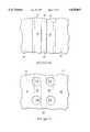
- FIG. 4is a top view of a portion of FIG. 3.
- FIG. 5is an alternate embodiment top view of a portion of FIG. 3.
- FIG. 6is a view of the FIG. 1 wafer at a processing step subsequent to that shown by FIG. 3.
- FIG. 7is a view of the FIG. 1 wafer at a processing step subsequent to that shown by FIG. 6.
- FIG. 8is a view of the FIG. 1 wafer at a processing step subsequent to that shown by FIG. 7.
- FIG. 9is a diagrammatic sectional view of an alternate embodiment semiconductor wafer fragment at one processing step in accordance with the invention.
- FIG. 10is a view of the FIG. 9 wafer at a processing step subsequent to that shown by FIG. 9.
- FIG. 11is a view of the FIG. 9 wafer at a processing step subsequent to that shown by FIG. 10.
- FIG. 12is a schematic representation of a static random access memory cell processed in accordance with the invention.
- a semiconductor processing method of forming CMOS dynamic random access memory within a semiconductor substratecomprising an array area and an area peripheral to the array, the peripheral area comprising complementary n-type field effect transistors and p-type field effect transistors, comprises the following steps:
- first and second field effect transistor gatesin the peripheral substrate area, the first gate to be utilized for formation of an n-type field effect transistor, the second gate to be utilized for formation of a p-type field effect transistor, the first gate defining opposing peripheral substrate regions for formation of desired opposing n-type substrate active regions, the second gate defining opposing peripheral substrate regions for formation of desired opposing p-type substrate active regions;
- the plugshaving an n-type dopant impurity concentration of at least 1 ⁇ 10 20 ions/cm 3 the desired n-type regions having an n-type dopant concentration prior to the filling step which is in the range of from 0 ions/cm 3 to 1 ⁇ 10 19 ions/cm 3 ;
- the memory cellscomprising a series of n-type field effect transistors and associated capacitors.
- a semiconductor processing method of forming CMOS static random access memory within a semiconductor substratecomprises the following steps:
- first, second, third and fourth field effect transistor gateson the substrate, the first and second gates to be utilized for formation of cross-coupled SRAM n-type field effect driver transistors, the third and fourth gates to be utilized for formation of SRAM p-type field effect load transistors, the first and second gates defining respective opposing substrate regions for formation of desired opposing n-type substrate active regions, the third and fourth gates defining respective opposing substrate regions for formation of desired opposing p-type substrate active regions;
- the plugshaving an n-type dopant impurity concentration of at least 1 ⁇ 10 20 ions/cm 3 , the desired n-type regions having an n-type dopant concentration prior to the filling step which is in the range of from 0 ions/cm 3 to 1 ⁇ 10 19 ions/cm 3 ;
- Fragment 10is comprised of a bulk silicon substrate 12 having isolation field oxide regions 14 formed therewithin. Fragment 10 comprises a memory array area 16 within which the principal and numerous memory cells will be provided, and a peripheral area 18.
- First and second field effect transistor gates 20 and 22, respectively,are provided in peripheral substrate area 18, while an array gate 24 is provided in array area 16. Voluminous other transistors would, of course, typically be provided on the wafer, with only the pertinent few to the preferred embodiment being shown for clarity.
- Each transistor gateis comprised of a typical gate oxide 26, overlying conductive polysilicon region 28, a higher conductivity silicide capping layer 30, and a concluding electrically insulative cap 32 (numbered in a portion of FIG. 1 only, for clarity).
- first gate 20will be utilized for formation of an n-type field effect transistor
- second gate 22will be utilized for formation of a p-type field effect transistor.
- first gate 20defines opposing peripheral substrate regions 34 for formation of desired opposing n-type substrate active regions.
- second gate 22defines opposing peripheral substrate regions 36 for formation of desired opposing p-type substrate active regions.
- array transistor 24is NMOS, with gate 24 thus defining opposing array substrate regions 38 for formation of desired source/drain diffusion regions within the array.
- a blanket n-type dopant implant to a substrate concentration of less than 1 ⁇ 10 19 ions/cm 3is provided into the desired n-type regions 34, 38 and the desired p-type regions 36, thus producing the illustrated implant regions 40.
- Suchwill be utilized to form lightly-doped-drain (LDD) regions of the NMOS transistors.
- LDDlightly-doped-drain
- a typical and preferred dopant concentration for regions 40is 1 ⁇ 10 18 ions/cm 3 .
- first gate 20, array gate 24, and desired n-type regions 34 and 38are masked with photoresist 44 while conducting overwhelming p-type conductivity doping into the desired p-type regions 36 of the peripheral substrate area, thus forming p-type implant regions 42.
- the typical and preferred dose for the implantis 5 ⁇ 10 15 ions/cm 2 -1 ⁇ 10 16 ions/cm 2 to produce an average 42 region dopant density of 5 ⁇ 10 19 ions/cm 3 -1 ⁇ 10 21 ions/cm 3 . This the p-type doping for the PMOS transistors overwhelms or overcompensates the previous LDD doping.
- oxide spacers 46are provided about the illustrated transistor gates utilizing conventional oxide deposition and subsequent anisotropic spacer etching.
- an insulating layer 48preferably borophosphosilicate glass (BPSG) is provided over the substrate, and accordingly over peripheral substrate area 18 over desired n-type regions 34 and p-type doped regions 42.
- Electrically insulating layer 48is thereafter patterned to provide a void 50 therethrough to each desired n-type region 34 and 38.
- voids 50are in the shape of elongated troughs for formation of continuous NMOS active areas.
- voids 50acould comprise substantially circular cross-sectioned contact openings for formation of discontinuous NMOS active areas.
- voids 50are filled with an n-type conductively doped polysilicon material, thus providing conductive plugs 52.
- the desired n-type regions 34 and 38will have an n-type dopant concentration prior to the filling step which is in the range of from 0 ion/cm 3 to 1 ⁇ 10 19 ions/cm 3 .
- Such plugswill have an n-type dopant impurity concentration of at least 1 ⁇ 10 20 ions/cm 3 with an impurity concentration of from 1 ⁇ 10 20 ions/cm 3 -5 ⁇ 10 20 ions/cm 3 , being preferred. Greater ion concentration would probably not be desirable in order to avoid short-channel effects within the resultant transistors.
- a preferred method for provision of polysilicon plugs 52would be by an in-situ doped polysilicon layer, followed by chemical-mechanical planarizing such poly and insulating layer 48 back to produce the FIG. 6 illustrated construction.
- substrate 10is annealed for a period of time effective to out-diffuse n-type dopant impurity from n-type conductively doped polysilicon plugs 52 into substrate 12 to form desired n-type active regions 54 and 56 having an n-type dopant impurity concentration of at least 1 ⁇ 10 20 ions/cm 3 in the substrate.
- An example annealwould be to subject the wafer to a temperature of 800° C. in an inert environment for 10 minutes. Most preferably, a dedicated anneal step is not conducted when subsequent wafer processing steps would inherently subject the wafer to temperature conditions for a time period suitable to cause the diffusion into the substrate.
- subsequent processingis conducted to produce a series of dynamic random access memory cells within the array, with one such cell being indicated by reference numeral 58.
- Suchcomprises a capacitor 60 having a storage node cell plate 62, capacitor dielectric layer 64, and cell capacitor plate 66.
- An encapsulating insulating layer 68is provided, with a conductive plug 70 provided therethrough to the illustrated plug 52.
- a conductive layeris deposited and patterned to form a bit line 72.
- FIGS. 9-11illustrate an alternate embodiment whereby a second blanket n-type dopant implant is provided after the first blanket implant of FIG. 1 and after the spacer formation.
- a second blanket n-type dopant implantis provided to a substrate concentration of from 1 ⁇ 10 19 ions/cm 3 to 5 ⁇ 10 20 ions/cm 3 into regions 34, 36 and 38, thus producing n-type implant regions 74.
- Suchmight be desirable to assure adequate concentration in the resultant n-type active regions 54 and 56 (FIG. 7) in the event desirable or adequate dopant out-diffusion from plugs 52 does not occur.
- a photoresist mask 44is provided, followed by a subsequent p-type doping to produce p-type regions 42.
- Such dopingis conducted at a level, such as in the previous embodiment, to assure overwhelming or overcompensating the n-type material of regions 36 with p-type material, such that the result is a PMOS construction.
- subsequent processingis conducted to provide polysilicon plugs 52.
- Subsequent annealdrives n-type dopant from plugs 52 into areas 74 to produce the composite n-type active area regions having an n-type dopant impurity concentration of at least 1 ⁇ 10 20 ions/cm 3 .
- the inventionalso has applicability to semiconductor processing methods of forming CMOS static random access memory circuitry within a semiconductor substrate.
- Such circuitryis illustrated in FIG. 12 and indicated generally with reference numeral 75.
- Suchcomprises first and second inverters 76 and 78 which are cross-coupled to form a bistable flip-flop.
- Inverters 76 and 78are formed by n-channel driver transistors 79 and 80 and p-channel load transistors 81 and 83.
- transistors 79, 80, 81 and 82constitute first, second, third and fourth field effect transistor gates, respectively.
- Driver transistor 79has active source regions 83 and 84, while driver transistor 80 comprises substrate active regions 85 and 86.
- p-type load transistor 81comprises substrate active regions 87 and 88, with p-type load transistor 82 having active substrate regions 89 and 90. Processing is provided as shown and described above with respect to the first described embodiment to produce doping polysilicon plugs which extend outwardly or upwardly from active regions 83, 84, 85 and 86.
- the conductive plugs of active regions 84 and 86are electrically connected with one another, and are tied to a low reference or circuit supply voltage, labeled V SS , and typically referred to as "ground.”
- Active regions 87 and 89 of load transistors 81 and 82, respectively,are connected in series between a high reference or circuit supply voltage, labeled V cc , and the drains of the corresponding driver transistors 79 and 80.
- the gates of load transistors 81 and 82are connected to the gates of the corresponding driver transistors 79 and 80.
- the conductive plug of active region 83 of first driver transistor 79is electrically interconnected with the gate of second driver transistor 80 via an electrical interconnect line 103, and with p-type active region 88 of load transistor 81.
- the conductive plug connecting with second driver transistor 80 active region 85electrically interconnects with the gate of first driver transistor 79 via an interconnect line 101, and with p-type active region 90 of p-type load transistor 82.
- Inverter 76has an inverter output 91 electrically connecting with or extending from active regions 83 and 88.
- inverter 78has an inverter output 92 electrically connecting with or extending outwardly from active regions 85 and 90.
- Lines 101 and 103provide additional respective inverter outputs.
- inverter output 91is cross-coupled to inverter output 103
- inverter output 92is cross-coupled to inverter input 101.
- inverter outputs 91 and 92form the complementary two-state outputs of the flip-flop.
- a memory flip-flopsuch as that just described forms one memory element of an integrated array of static memory elements.
- a plurality of access transistorssuch as access transistors 93 and 94, are used to selectively address and access individual memory elements within the array.
- Access transistor 93preferably comprises an n-channel MOSFET having one active terminal connected to cross-coupled inverter output 103.
- a plurality of complementary column line pairssuch as the single pair of complementary column lines 95 and 96, are connected to the remaining active terminals of access transistors 93 and 94, respectively.
- a row line 97is connected to the gates of access transistors 93 and 94.
Landscapes
- Metal-Oxide And Bipolar Metal-Oxide Semiconductor Integrated Circuits (AREA)
- Semiconductor Memories (AREA)
Abstract
Description
Claims (26)
Priority Applications (2)
| Application Number | Priority Date | Filing Date | Title |
|---|---|---|---|
| US08/503,199US5624863A (en) | 1995-07-17 | 1995-07-17 | Semiconductor processing method of forming complementary N-type doped and P-type doped active regions within a semiconductor substrate |
| US08/797,547US5970335A (en) | 1995-07-17 | 1997-02-07 | Semiconductor processing method of forming complementary n-type doped and p-type doped active regions within a semiconductor substrate |
Applications Claiming Priority (1)
| Application Number | Priority Date | Filing Date | Title |
|---|---|---|---|
| US08/503,199US5624863A (en) | 1995-07-17 | 1995-07-17 | Semiconductor processing method of forming complementary N-type doped and P-type doped active regions within a semiconductor substrate |
Related Child Applications (1)
| Application Number | Title | Priority Date | Filing Date |
|---|---|---|---|
| US08/797,547ContinuationUS5970335A (en) | 1995-07-17 | 1997-02-07 | Semiconductor processing method of forming complementary n-type doped and p-type doped active regions within a semiconductor substrate |
Publications (1)
| Publication Number | Publication Date |
|---|---|
| US5624863Atrue US5624863A (en) | 1997-04-29 |
Family
ID=24001119
Family Applications (2)
| Application Number | Title | Priority Date | Filing Date |
|---|---|---|---|
| US08/503,199Expired - LifetimeUS5624863A (en) | 1995-07-17 | 1995-07-17 | Semiconductor processing method of forming complementary N-type doped and P-type doped active regions within a semiconductor substrate |
| US08/797,547Expired - LifetimeUS5970335A (en) | 1995-07-17 | 1997-02-07 | Semiconductor processing method of forming complementary n-type doped and p-type doped active regions within a semiconductor substrate |
Family Applications After (1)
| Application Number | Title | Priority Date | Filing Date |
|---|---|---|---|
| US08/797,547Expired - LifetimeUS5970335A (en) | 1995-07-17 | 1997-02-07 | Semiconductor processing method of forming complementary n-type doped and p-type doped active regions within a semiconductor substrate |
Country Status (1)
| Country | Link |
|---|---|
| US (2) | US5624863A (en) |
Cited By (75)
| Publication number | Priority date | Publication date | Assignee | Title |
|---|---|---|---|---|
| US5811329A (en)* | 1996-06-03 | 1998-09-22 | Micron Technology, Inc. | Method of forming CMOS circuitry including patterning a layer of conductive material overlying field isolation oxide |
| US5843834A (en)* | 1996-08-08 | 1998-12-01 | National Semiconductor Corporation | Self-aligned POCL3 process flow for submicron microelectronics applications using amorphized polysilicon |
| US5981324A (en)* | 1996-10-23 | 1999-11-09 | Samsung Electronics Co., Ltd. | Methods of forming integrated circuits having memory cell arrays and peripheral circuits therein |
| US6060345A (en)* | 1997-04-21 | 2000-05-09 | Advanced Micro Devices, Inc. | Method of making NMOS and PMOS devices with reduced masking steps |
| US6080613A (en)* | 1995-12-15 | 2000-06-27 | Samsung Electronics Co., Ltd. | Methods of forming integrated circuit memory devices having improved bit line and storage electrode contact regions therein |
| US6087253A (en)* | 1998-03-03 | 2000-07-11 | Vanguard International Semiconductor Corporation | Method of forming landing plugs for PMOS and NMOS |
| US6104045A (en)* | 1998-05-13 | 2000-08-15 | Micron Technology, Inc. | High density planar SRAM cell using bipolar latch-up and gated diode breakdown |
| US6128216A (en)* | 1998-05-13 | 2000-10-03 | Micron Technology Inc. | High density planar SRAM cell with merged transistors |
| US6163059A (en)* | 1997-03-07 | 2000-12-19 | Advanced Micro Devices, Inc. | Integrated circuit including source implant self-aligned to contact via |
| US6214680B1 (en) | 1999-12-13 | 2001-04-10 | Chartered Semiconductor Manufacturing, Ltd. | Method to fabricate a sub-quarter-micron MOSFET with lightly doped source/drain regions |
| US6225165B1 (en) | 1998-05-13 | 2001-05-01 | Micron Technology, Inc. | High density SRAM cell with latched vertical transistors |
| US20010010386A1 (en)* | 1997-07-31 | 2001-08-02 | Tsukasa Yajima | Semiconductor device having protective layer on field oxide |
| US6281058B1 (en)* | 1996-03-07 | 2001-08-28 | Micron Technology, Inc. | Method of forming DRAM circuitry on a semiconductor substrate |
| US6312997B1 (en) | 1998-08-12 | 2001-11-06 | Micron Technology, Inc. | Low voltage high performance semiconductor devices and methods |
| US6329273B1 (en)* | 1999-10-29 | 2001-12-11 | Advanced Micro Devices, Inc. | Solid-source doping for source/drain to eliminate implant damage |
| US6333535B2 (en) | 1998-08-06 | 2001-12-25 | Mitsubishi Denki Kabushiki Kaisha | Semiconductor device |
| US6346447B1 (en)* | 1997-08-29 | 2002-02-12 | Texas Instruments Incorporated | Shallow-implant elevated source/drain doping from a sidewall dopant source |
| US6391702B1 (en)* | 1999-10-29 | 2002-05-21 | Nec Corporation | Method of manufacture for semiconductor devices |
| US6492674B1 (en)* | 1999-12-16 | 2002-12-10 | Mitsubishi Denki Kabushiki Kaisha | Semiconductor device having an improved plug structure and method of manufacturing the same |
| US6503790B2 (en) | 1998-05-13 | 2003-01-07 | Micron Technology, Inc. | High density vertical SRAM cell using bipolar latchup induced by gated diode breakdown |
| US6627490B2 (en)* | 1999-08-30 | 2003-09-30 | Nec Electronics Corporation | Semiconductor device and method for fabricating the same |
| US20050017285A1 (en)* | 2003-05-15 | 2005-01-27 | Kuo-Chyuan Tzeng | Novel embedded dual-port DRAM process |
| US20060071074A1 (en)* | 2004-09-29 | 2006-04-06 | Matrix Semiconductor, Inc. | Doped polysilicon via connecting polysilicon layers |
| US20060145274A1 (en)* | 2003-09-23 | 2006-07-06 | International Business Machines Corporation | NFETs using gate induced stress modulation |
| US20100035429A1 (en)* | 2007-01-18 | 2010-02-11 | Terasemicon Corporation | Method for fabricating semiconductor device |
| WO2013025656A1 (en) | 2011-08-12 | 2013-02-21 | Gsi Technology, Inc. | Systems and methods involving multi-bank, dual- or multi-pipe srams |
| US8404551B2 (en) | 2010-12-03 | 2013-03-26 | Suvolta, Inc. | Source/drain extension control for advanced transistors |
| US8421162B2 (en) | 2009-09-30 | 2013-04-16 | Suvolta, Inc. | Advanced transistors with punch through suppression |
| US8461875B1 (en) | 2011-02-18 | 2013-06-11 | Suvolta, Inc. | Digital circuits having improved transistors, and methods therefor |
| US8525271B2 (en) | 2011-03-03 | 2013-09-03 | Suvolta, Inc. | Semiconductor structure with improved channel stack and method for fabrication thereof |
| US8530286B2 (en) | 2010-04-12 | 2013-09-10 | Suvolta, Inc. | Low power semiconductor transistor structure and method of fabrication thereof |
| US8569156B1 (en) | 2011-05-16 | 2013-10-29 | Suvolta, Inc. | Reducing or eliminating pre-amorphization in transistor manufacture |
| US8569128B2 (en) | 2010-06-21 | 2013-10-29 | Suvolta, Inc. | Semiconductor structure and method of fabrication thereof with mixed metal types |
| US8599623B1 (en) | 2011-12-23 | 2013-12-03 | Suvolta, Inc. | Circuits and methods for measuring circuit elements in an integrated circuit device |
| US8614128B1 (en) | 2011-08-23 | 2013-12-24 | Suvolta, Inc. | CMOS structures and processes based on selective thinning |
| US8629016B1 (en) | 2011-07-26 | 2014-01-14 | Suvolta, Inc. | Multiple transistor types formed in a common epitaxial layer by differential out-diffusion from a doped underlayer |
| US8637955B1 (en) | 2012-08-31 | 2014-01-28 | Suvolta, Inc. | Semiconductor structure with reduced junction leakage and method of fabrication thereof |
| US8645878B1 (en) | 2011-08-23 | 2014-02-04 | Suvolta, Inc. | Porting a circuit design from a first semiconductor process to a second semiconductor process |
| US8713511B1 (en) | 2011-09-16 | 2014-04-29 | Suvolta, Inc. | Tools and methods for yield-aware semiconductor manufacturing process target generation |
| US8735987B1 (en) | 2011-06-06 | 2014-05-27 | Suvolta, Inc. | CMOS gate stack structures and processes |
| US8748270B1 (en) | 2011-03-30 | 2014-06-10 | Suvolta, Inc. | Process for manufacturing an improved analog transistor |
| US8748986B1 (en) | 2011-08-05 | 2014-06-10 | Suvolta, Inc. | Electronic device with controlled threshold voltage |
| US8759872B2 (en) | 2010-06-22 | 2014-06-24 | Suvolta, Inc. | Transistor with threshold voltage set notch and method of fabrication thereof |
| US8796048B1 (en) | 2011-05-11 | 2014-08-05 | Suvolta, Inc. | Monitoring and measurement of thin film layers |
| US8811068B1 (en) | 2011-05-13 | 2014-08-19 | Suvolta, Inc. | Integrated circuit devices and methods |
| US8819603B1 (en) | 2011-12-15 | 2014-08-26 | Suvolta, Inc. | Memory circuits and methods of making and designing the same |
| US8816754B1 (en) | 2012-11-02 | 2014-08-26 | Suvolta, Inc. | Body bias circuits and methods |
| US8863064B1 (en) | 2012-03-23 | 2014-10-14 | Suvolta, Inc. | SRAM cell layout structure and devices therefrom |
| US8877619B1 (en) | 2012-01-23 | 2014-11-04 | Suvolta, Inc. | Process for manufacture of integrated circuits with different channel doping transistor architectures and devices therefrom |
| US8883600B1 (en) | 2011-12-22 | 2014-11-11 | Suvolta, Inc. | Transistor having reduced junction leakage and methods of forming thereof |
| US8895327B1 (en) | 2011-12-09 | 2014-11-25 | Suvolta, Inc. | Tipless transistors, short-tip transistors, and methods and circuits therefor |
| US8970289B1 (en) | 2012-01-23 | 2015-03-03 | Suvolta, Inc. | Circuits and devices for generating bi-directional body bias voltages, and methods therefor |
| US8995204B2 (en) | 2011-06-23 | 2015-03-31 | Suvolta, Inc. | Circuit devices and methods having adjustable transistor body bias |
| US8999861B1 (en) | 2011-05-11 | 2015-04-07 | Suvolta, Inc. | Semiconductor structure with substitutional boron and method for fabrication thereof |
| US9041126B2 (en) | 2012-09-21 | 2015-05-26 | Mie Fujitsu Semiconductor Limited | Deeply depleted MOS transistors having a screening layer and methods thereof |
| US9054219B1 (en) | 2011-08-05 | 2015-06-09 | Mie Fujitsu Semiconductor Limited | Semiconductor devices having fin structures and fabrication methods thereof |
| US9070477B1 (en) | 2012-12-12 | 2015-06-30 | Mie Fujitsu Semiconductor Limited | Bit interleaved low voltage static random access memory (SRAM) and related methods |
| US9093550B1 (en) | 2012-01-31 | 2015-07-28 | Mie Fujitsu Semiconductor Limited | Integrated circuits having a plurality of high-K metal gate FETs with various combinations of channel foundation structure and gate stack structure and methods of making same |
| US9093997B1 (en) | 2012-11-15 | 2015-07-28 | Mie Fujitsu Semiconductor Limited | Slew based process and bias monitors and related methods |
| US9112057B1 (en) | 2012-09-18 | 2015-08-18 | Mie Fujitsu Semiconductor Limited | Semiconductor devices with dopant migration suppression and method of fabrication thereof |
| US9112484B1 (en) | 2012-12-20 | 2015-08-18 | Mie Fujitsu Semiconductor Limited | Integrated circuit process and bias monitors and related methods |
| US20150340451A1 (en)* | 2014-05-26 | 2015-11-26 | Semiconductor Manufacturing International (Shanghai) Corporation | Method for cmp of high-k metal gate structures |
| US9236466B1 (en) | 2011-10-07 | 2016-01-12 | Mie Fujitsu Semiconductor Limited | Analog circuits having improved insulated gate transistors, and methods therefor |
| US9268885B1 (en) | 2013-02-28 | 2016-02-23 | Mie Fujitsu Semiconductor Limited | Integrated circuit device methods and models with predicted device metric variations |
| US9299801B1 (en) | 2013-03-14 | 2016-03-29 | Mie Fujitsu Semiconductor Limited | Method for fabricating a transistor device with a tuned dopant profile |
| US9299698B2 (en) | 2012-06-27 | 2016-03-29 | Mie Fujitsu Semiconductor Limited | Semiconductor structure with multiple transistors having various threshold voltages |
| US9318174B1 (en) | 2013-03-15 | 2016-04-19 | Gsi Technology, Inc. | Memory systems and methods involving high speed local address circuitry |
| US9319013B2 (en) | 2014-08-19 | 2016-04-19 | Mie Fujitsu Semiconductor Limited | Operational amplifier input offset correction with transistor threshold voltage adjustment |
| US9406567B1 (en) | 2012-02-28 | 2016-08-02 | Mie Fujitsu Semiconductor Limited | Method for fabricating multiple transistor devices on a substrate with varying threshold voltages |
| US9431068B2 (en) | 2012-10-31 | 2016-08-30 | Mie Fujitsu Semiconductor Limited | Dynamic random access memory (DRAM) with low variation transistor peripheral circuits |
| US9478571B1 (en) | 2013-05-24 | 2016-10-25 | Mie Fujitsu Semiconductor Limited | Buried channel deeply depleted channel transistor |
| US9710006B2 (en) | 2014-07-25 | 2017-07-18 | Mie Fujitsu Semiconductor Limited | Power up body bias circuits and methods |
| US10074568B2 (en) | 2009-09-30 | 2018-09-11 | Mie Fujitsu Semiconductor Limited | Electronic devices and systems, and methods for making and using same |
| US20190148231A1 (en)* | 2016-04-12 | 2019-05-16 | Sun Yat-Sen University | Mos transistor for suppressing generation of photo-induced leakage current in active channel region and application thereof |
| WO2025137037A1 (en) | 2023-12-18 | 2025-06-26 | L'oreal | Gel compositions containing bis-ethylhexyloxyphenol methoxyphenyl triazine and sugar fatty acid ester gelling agent |
Families Citing this family (3)
| Publication number | Priority date | Publication date | Assignee | Title |
|---|---|---|---|---|
| US6207491B1 (en)* | 1999-02-25 | 2001-03-27 | Vanguard International Semiconductor Corporation | Method for preventing silicon substrate loss in fabricating semiconductor device |
| US6849492B2 (en)* | 2002-07-08 | 2005-02-01 | Micron Technology, Inc. | Method for forming standard voltage threshold and low voltage threshold MOSFET devices |
| KR100903460B1 (en)* | 2002-12-30 | 2009-06-18 | 동부일렉트로닉스 주식회사 | Memory cell manufacturing method having a gap filling layer forming step and its structure |
Citations (3)
| Publication number | Priority date | Publication date | Assignee | Title |
|---|---|---|---|---|
| US5145799A (en)* | 1991-01-30 | 1992-09-08 | Texas Instruments Incorporated | Stacked capacitor SRAM cell |
| US5179033A (en)* | 1990-09-05 | 1993-01-12 | Sharp Kabushiki Kaisha | Method for manufacturing tft sram |
| US5204279A (en)* | 1991-06-03 | 1993-04-20 | Sgs-Thomson Microelectronics, Inc. | Method of making SRAM cell and structure with polycrystalline p-channel load devices |
Family Cites Families (3)
| Publication number | Priority date | Publication date | Assignee | Title |
|---|---|---|---|---|
| US4707457A (en)* | 1986-04-03 | 1987-11-17 | Advanced Micro Devices, Inc. | Method for making improved contact for integrated circuit structure |
| US5422289A (en)* | 1992-04-27 | 1995-06-06 | National Semiconductor Corporation | Method of manufacturing a fully planarized MOSFET and resulting structure |
| US5571733A (en)* | 1995-05-12 | 1996-11-05 | Micron Technology, Inc. | Method of forming CMOS integrated circuitry |
- 1995
- 1995-07-17USUS08/503,199patent/US5624863A/ennot_activeExpired - Lifetime
- 1997
- 1997-02-07USUS08/797,547patent/US5970335A/ennot_activeExpired - Lifetime
Patent Citations (3)
| Publication number | Priority date | Publication date | Assignee | Title |
|---|---|---|---|---|
| US5179033A (en)* | 1990-09-05 | 1993-01-12 | Sharp Kabushiki Kaisha | Method for manufacturing tft sram |
| US5145799A (en)* | 1991-01-30 | 1992-09-08 | Texas Instruments Incorporated | Stacked capacitor SRAM cell |
| US5204279A (en)* | 1991-06-03 | 1993-04-20 | Sgs-Thomson Microelectronics, Inc. | Method of making SRAM cell and structure with polycrystalline p-channel load devices |
Cited By (146)
| Publication number | Priority date | Publication date | Assignee | Title |
|---|---|---|---|---|
| US6080613A (en)* | 1995-12-15 | 2000-06-27 | Samsung Electronics Co., Ltd. | Methods of forming integrated circuit memory devices having improved bit line and storage electrode contact regions therein |
| US6281058B1 (en)* | 1996-03-07 | 2001-08-28 | Micron Technology, Inc. | Method of forming DRAM circuitry on a semiconductor substrate |
| US5923977A (en)* | 1996-06-03 | 1999-07-13 | Micron Technology, Inc. | Method of forming CMOS circuitry including patterning a layer of conductive material overlying field isolation oxide |
| US6136637A (en)* | 1996-06-03 | 2000-10-24 | Micron Technology, Inc. | Method of forming CMOS circuitry including patterning conductive material overlying field isolation oxide |
| US5811329A (en)* | 1996-06-03 | 1998-09-22 | Micron Technology, Inc. | Method of forming CMOS circuitry including patterning a layer of conductive material overlying field isolation oxide |
| US5843834A (en)* | 1996-08-08 | 1998-12-01 | National Semiconductor Corporation | Self-aligned POCL3 process flow for submicron microelectronics applications using amorphized polysilicon |
| US5981324A (en)* | 1996-10-23 | 1999-11-09 | Samsung Electronics Co., Ltd. | Methods of forming integrated circuits having memory cell arrays and peripheral circuits therein |
| US6163059A (en)* | 1997-03-07 | 2000-12-19 | Advanced Micro Devices, Inc. | Integrated circuit including source implant self-aligned to contact via |
| US6060345A (en)* | 1997-04-21 | 2000-05-09 | Advanced Micro Devices, Inc. | Method of making NMOS and PMOS devices with reduced masking steps |
| US20010010386A1 (en)* | 1997-07-31 | 2001-08-02 | Tsukasa Yajima | Semiconductor device having protective layer on field oxide |
| US6346447B1 (en)* | 1997-08-29 | 2002-02-12 | Texas Instruments Incorporated | Shallow-implant elevated source/drain doping from a sidewall dopant source |
| US6087253A (en)* | 1998-03-03 | 2000-07-11 | Vanguard International Semiconductor Corporation | Method of forming landing plugs for PMOS and NMOS |
| US6225165B1 (en) | 1998-05-13 | 2001-05-01 | Micron Technology, Inc. | High density SRAM cell with latched vertical transistors |
| US20010002062A1 (en)* | 1998-05-13 | 2001-05-31 | Noble Wendell P. | High density SRAM cell with latched vertical transistors |
| US6545297B1 (en) | 1998-05-13 | 2003-04-08 | Micron Technology, Inc. | High density vertical SRAM cell using bipolar latchup induced by gated diode breakdown |
| US6128216A (en)* | 1998-05-13 | 2000-10-03 | Micron Technology Inc. | High density planar SRAM cell with merged transistors |
| US20060216870A1 (en)* | 1998-05-13 | 2006-09-28 | Noble Wendell P Jr | High density SRAM cell with latched vertical transistors |
| US7105386B2 (en) | 1998-05-13 | 2006-09-12 | Micron Technology, Inc. | High density SRAM cell with latched vertical transistors |
| US6104045A (en)* | 1998-05-13 | 2000-08-15 | Micron Technology, Inc. | High density planar SRAM cell using bipolar latch-up and gated diode breakdown |
| US6936886B2 (en) | 1998-05-13 | 2005-08-30 | Micron Technology, Inc. | High density SRAM cell with latched vertical transistors |
| US20040171219A1 (en)* | 1998-05-13 | 2004-09-02 | Noble Wendell P. | High density SRAM cell with latched vertical transistors |
| US6773968B1 (en) | 1998-05-13 | 2004-08-10 | Micron Technology, Inc. | High density planar SRAM cell using bipolar latch-up and gated diode breakdown |
| US6503790B2 (en) | 1998-05-13 | 2003-01-07 | Micron Technology, Inc. | High density vertical SRAM cell using bipolar latchup induced by gated diode breakdown |
| US6333535B2 (en) | 1998-08-06 | 2001-12-25 | Mitsubishi Denki Kabushiki Kaisha | Semiconductor device |
| US20040198004A1 (en)* | 1998-08-12 | 2004-10-07 | Tran Luan C | Low voltage high performance semiconductor devices and methods |
| US6312997B1 (en) | 1998-08-12 | 2001-11-06 | Micron Technology, Inc. | Low voltage high performance semiconductor devices and methods |
| US6747326B2 (en) | 1998-08-12 | 2004-06-08 | Micron Technology, Inc. | Low voltage high performance semiconductor device having punch through prevention implants |
| US6492693B2 (en) | 1998-08-12 | 2002-12-10 | Micron Technology, Inc. | Low voltage high performance semiconductor devices and methods |
| US6946353B2 (en)* | 1998-08-12 | 2005-09-20 | Micron Technology, Inc. | Low voltage high performance semiconductor devices and methods |
| US6627490B2 (en)* | 1999-08-30 | 2003-09-30 | Nec Electronics Corporation | Semiconductor device and method for fabricating the same |
| US6391702B1 (en)* | 1999-10-29 | 2002-05-21 | Nec Corporation | Method of manufacture for semiconductor devices |
| US6329273B1 (en)* | 1999-10-29 | 2001-12-11 | Advanced Micro Devices, Inc. | Solid-source doping for source/drain to eliminate implant damage |
| US6214680B1 (en) | 1999-12-13 | 2001-04-10 | Chartered Semiconductor Manufacturing, Ltd. | Method to fabricate a sub-quarter-micron MOSFET with lightly doped source/drain regions |
| US6492674B1 (en)* | 1999-12-16 | 2002-12-10 | Mitsubishi Denki Kabushiki Kaisha | Semiconductor device having an improved plug structure and method of manufacturing the same |
| US20050017285A1 (en)* | 2003-05-15 | 2005-01-27 | Kuo-Chyuan Tzeng | Novel embedded dual-port DRAM process |
| US7091543B2 (en)* | 2003-05-15 | 2006-08-15 | Taiwan Semiconductor Manufacturing Co., Ltd. | Embedded dual-port DRAM process |
| US20060145274A1 (en)* | 2003-09-23 | 2006-07-06 | International Business Machines Corporation | NFETs using gate induced stress modulation |
| US7915163B2 (en)* | 2004-09-29 | 2011-03-29 | Sandisk 3D Llc | Method for forming doped polysilicon via connecting polysilicon layers |
| US7566974B2 (en)* | 2004-09-29 | 2009-07-28 | Sandisk 3D, Llc | Doped polysilicon via connecting polysilicon layers |
| US20090258462A1 (en)* | 2004-09-29 | 2009-10-15 | Konevecki Michael W | Method for forming doped polysilicon via connecting polysilicon layers |
| US20060071074A1 (en)* | 2004-09-29 | 2006-04-06 | Matrix Semiconductor, Inc. | Doped polysilicon via connecting polysilicon layers |
| US20110021019A1 (en)* | 2004-09-29 | 2011-01-27 | Konevecki Michael W | Method for forming doped polysilicon via connecting polysilicon layers |
| US7915164B2 (en) | 2004-09-29 | 2011-03-29 | Sandisk 3D Llc | Method for forming doped polysilicon via connecting polysilicon layers |
| US20100035429A1 (en)* | 2007-01-18 | 2010-02-11 | Terasemicon Corporation | Method for fabricating semiconductor device |
| US7928008B2 (en)* | 2007-01-18 | 2011-04-19 | Terasemicon Corporation | Method for fabricating semiconductor device |
| US10325986B2 (en) | 2009-09-30 | 2019-06-18 | Mie Fujitsu Semiconductor Limited | Advanced transistors with punch through suppression |
| US10224244B2 (en) | 2009-09-30 | 2019-03-05 | Mie Fujitsu Semiconductor Limited | Electronic devices and systems, and methods for making and using the same |
| US8421162B2 (en) | 2009-09-30 | 2013-04-16 | Suvolta, Inc. | Advanced transistors with punch through suppression |
| US10217668B2 (en) | 2009-09-30 | 2019-02-26 | Mie Fujitsu Semiconductor Limited | Electronic devices and systems, and methods for making and using the same |
| US9263523B2 (en) | 2009-09-30 | 2016-02-16 | Mie Fujitsu Semiconductor Limited | Advanced transistors with punch through suppression |
| US11887895B2 (en) | 2009-09-30 | 2024-01-30 | United Semiconductor Japan Co., Ltd. | Electronic devices and systems, and methods for making and using the same |
| US10074568B2 (en) | 2009-09-30 | 2018-09-11 | Mie Fujitsu Semiconductor Limited | Electronic devices and systems, and methods for making and using same |
| US9508800B2 (en) | 2009-09-30 | 2016-11-29 | Mie Fujitsu Semiconductor Limited | Advanced transistors with punch through suppression |
| US11062950B2 (en) | 2009-09-30 | 2021-07-13 | United Semiconductor Japan Co., Ltd. | Electronic devices and systems, and methods for making and using the same |
| US8530286B2 (en) | 2010-04-12 | 2013-09-10 | Suvolta, Inc. | Low power semiconductor transistor structure and method of fabrication thereof |
| US9865596B2 (en) | 2010-04-12 | 2018-01-09 | Mie Fujitsu Semiconductor Limited | Low power semiconductor transistor structure and method of fabrication thereof |
| US9496261B2 (en) | 2010-04-12 | 2016-11-15 | Mie Fujitsu Semiconductor Limited | Low power semiconductor transistor structure and method of fabrication thereof |
| US8569128B2 (en) | 2010-06-21 | 2013-10-29 | Suvolta, Inc. | Semiconductor structure and method of fabrication thereof with mixed metal types |
| US9224733B2 (en) | 2010-06-21 | 2015-12-29 | Mie Fujitsu Semiconductor Limited | Semiconductor structure and method of fabrication thereof with mixed metal types |
| US9922977B2 (en) | 2010-06-22 | 2018-03-20 | Mie Fujitsu Semiconductor Limited | Transistor with threshold voltage set notch and method of fabrication thereof |
| US9418987B2 (en) | 2010-06-22 | 2016-08-16 | Mie Fujitsu Semiconductor Limited | Transistor with threshold voltage set notch and method of fabrication thereof |
| US8759872B2 (en) | 2010-06-22 | 2014-06-24 | Suvolta, Inc. | Transistor with threshold voltage set notch and method of fabrication thereof |
| US8563384B2 (en) | 2010-12-03 | 2013-10-22 | Suvolta, Inc. | Source/drain extension control for advanced transistors |
| US8404551B2 (en) | 2010-12-03 | 2013-03-26 | Suvolta, Inc. | Source/drain extension control for advanced transistors |
| US9006843B2 (en) | 2010-12-03 | 2015-04-14 | Suvolta, Inc. | Source/drain extension control for advanced transistors |
| US8686511B2 (en) | 2010-12-03 | 2014-04-01 | Suvolta, Inc. | Source/drain extension control for advanced transistors |
| US8461875B1 (en) | 2011-02-18 | 2013-06-11 | Suvolta, Inc. | Digital circuits having improved transistors, and methods therefor |
| US9184750B1 (en) | 2011-02-18 | 2015-11-10 | Mie Fujitsu Semiconductor Limited | Digital circuits having improved transistors, and methods therefor |
| US9680470B2 (en) | 2011-02-18 | 2017-06-13 | Mie Fujitsu Semiconductor Limited | Digital circuits having improved transistors, and methods therefor |
| US9838012B2 (en) | 2011-02-18 | 2017-12-05 | Mie Fujitsu Semiconductor Limited | Digital circuits having improved transistors, and methods therefor |
| US10250257B2 (en) | 2011-02-18 | 2019-04-02 | Mie Fujitsu Semiconductor Limited | Digital circuits having improved transistors, and methods therefor |
| US9985631B2 (en) | 2011-02-18 | 2018-05-29 | Mie Fujitsu Semiconductor Limited | Digital circuits having improved transistors, and methods therefor |
| US8525271B2 (en) | 2011-03-03 | 2013-09-03 | Suvolta, Inc. | Semiconductor structure with improved channel stack and method for fabrication thereof |
| US9111785B2 (en) | 2011-03-03 | 2015-08-18 | Mie Fujitsu Semiconductor Limited | Semiconductor structure with improved channel stack and method for fabrication thereof |
| US8748270B1 (en) | 2011-03-30 | 2014-06-10 | Suvolta, Inc. | Process for manufacturing an improved analog transistor |
| US9093469B2 (en) | 2011-03-30 | 2015-07-28 | Mie Fujitsu Semiconductor Limited | Analog transistor |
| US8796048B1 (en) | 2011-05-11 | 2014-08-05 | Suvolta, Inc. | Monitoring and measurement of thin film layers |
| US8999861B1 (en) | 2011-05-11 | 2015-04-07 | Suvolta, Inc. | Semiconductor structure with substitutional boron and method for fabrication thereof |
| US9741428B2 (en) | 2011-05-13 | 2017-08-22 | Mie Fujitsu Semiconductor Limited | Integrated circuit devices and methods |
| US9362291B1 (en) | 2011-05-13 | 2016-06-07 | Mie Fujitsu Semiconductor Limited | Integrated circuit devices and methods |
| US9966130B2 (en) | 2011-05-13 | 2018-05-08 | Mie Fujitsu Semiconductor Limited | Integrated circuit devices and methods |
| US8811068B1 (en) | 2011-05-13 | 2014-08-19 | Suvolta, Inc. | Integrated circuit devices and methods |
| US9514940B2 (en) | 2011-05-16 | 2016-12-06 | Mie Fujitsu Semiconductor Limited | Reducing or eliminating pre-amorphization in transistor manufacture |
| US8937005B2 (en) | 2011-05-16 | 2015-01-20 | Suvolta, Inc. | Reducing or eliminating pre-amorphization in transistor manufacture |
| US8569156B1 (en) | 2011-05-16 | 2013-10-29 | Suvolta, Inc. | Reducing or eliminating pre-amorphization in transistor manufacture |
| US9793172B2 (en) | 2011-05-16 | 2017-10-17 | Mie Fujitsu Semiconductor Limited | Reducing or eliminating pre-amorphization in transistor manufacture |
| US9281248B1 (en) | 2011-06-06 | 2016-03-08 | Mie Fujitsu Semiconductor Limited | CMOS gate stack structures and processes |
| US8735987B1 (en) | 2011-06-06 | 2014-05-27 | Suvolta, Inc. | CMOS gate stack structures and processes |
| US8995204B2 (en) | 2011-06-23 | 2015-03-31 | Suvolta, Inc. | Circuit devices and methods having adjustable transistor body bias |
| US8653604B1 (en) | 2011-07-26 | 2014-02-18 | Suvolta, Inc. | Multiple transistor types formed in a common epitaxial layer by differential out-diffusion from a doped underlayer |
| US8916937B1 (en) | 2011-07-26 | 2014-12-23 | Suvolta, Inc. | Multiple transistor types formed in a common epitaxial layer by differential out-diffusion from a doped underlayer |
| US8629016B1 (en) | 2011-07-26 | 2014-01-14 | Suvolta, Inc. | Multiple transistor types formed in a common epitaxial layer by differential out-diffusion from a doped underlayer |
| US9054219B1 (en) | 2011-08-05 | 2015-06-09 | Mie Fujitsu Semiconductor Limited | Semiconductor devices having fin structures and fabrication methods thereof |
| US8963249B1 (en) | 2011-08-05 | 2015-02-24 | Suvolta, Inc. | Electronic device with controlled threshold voltage |
| US8748986B1 (en) | 2011-08-05 | 2014-06-10 | Suvolta, Inc. | Electronic device with controlled threshold voltage |
| WO2013025656A1 (en) | 2011-08-12 | 2013-02-21 | Gsi Technology, Inc. | Systems and methods involving multi-bank, dual- or multi-pipe srams |
| US8614128B1 (en) | 2011-08-23 | 2013-12-24 | Suvolta, Inc. | CMOS structures and processes based on selective thinning |
| US8645878B1 (en) | 2011-08-23 | 2014-02-04 | Suvolta, Inc. | Porting a circuit design from a first semiconductor process to a second semiconductor process |
| US9117746B1 (en) | 2011-08-23 | 2015-08-25 | Mie Fujitsu Semiconductor Limited | Porting a circuit design from a first semiconductor process to a second semiconductor process |
| US8806395B1 (en) | 2011-08-23 | 2014-08-12 | Suvolta, Inc. | Porting a circuit design from a first semiconductor process to a second semiconductor process |
| US9391076B1 (en) | 2011-08-23 | 2016-07-12 | Mie Fujitsu Semiconductor Limited | CMOS structures and processes based on selective thinning |
| US8713511B1 (en) | 2011-09-16 | 2014-04-29 | Suvolta, Inc. | Tools and methods for yield-aware semiconductor manufacturing process target generation |
| US9236466B1 (en) | 2011-10-07 | 2016-01-12 | Mie Fujitsu Semiconductor Limited | Analog circuits having improved insulated gate transistors, and methods therefor |
| US8895327B1 (en) | 2011-12-09 | 2014-11-25 | Suvolta, Inc. | Tipless transistors, short-tip transistors, and methods and circuits therefor |
| US8819603B1 (en) | 2011-12-15 | 2014-08-26 | Suvolta, Inc. | Memory circuits and methods of making and designing the same |
| US9368624B2 (en) | 2011-12-22 | 2016-06-14 | Mie Fujitsu Semiconductor Limited | Method for fabricating a transistor with reduced junction leakage current |
| US9196727B2 (en) | 2011-12-22 | 2015-11-24 | Mie Fujitsu Semiconductor Limited | High uniformity screen and epitaxial layers for CMOS devices |
| US8883600B1 (en) | 2011-12-22 | 2014-11-11 | Suvolta, Inc. | Transistor having reduced junction leakage and methods of forming thereof |
| US8599623B1 (en) | 2011-12-23 | 2013-12-03 | Suvolta, Inc. | Circuits and methods for measuring circuit elements in an integrated circuit device |
| US8877619B1 (en) | 2012-01-23 | 2014-11-04 | Suvolta, Inc. | Process for manufacture of integrated circuits with different channel doping transistor architectures and devices therefrom |
| US8970289B1 (en) | 2012-01-23 | 2015-03-03 | Suvolta, Inc. | Circuits and devices for generating bi-directional body bias voltages, and methods therefor |
| US9093550B1 (en) | 2012-01-31 | 2015-07-28 | Mie Fujitsu Semiconductor Limited | Integrated circuits having a plurality of high-K metal gate FETs with various combinations of channel foundation structure and gate stack structure and methods of making same |
| US9385047B2 (en) | 2012-01-31 | 2016-07-05 | Mie Fujitsu Semiconductor Limited | Integrated circuits having a plurality of high-K metal gate FETs with various combinations of channel foundation structure and gate stack structure and methods of making same |
| US9406567B1 (en) | 2012-02-28 | 2016-08-02 | Mie Fujitsu Semiconductor Limited | Method for fabricating multiple transistor devices on a substrate with varying threshold voltages |
| US8863064B1 (en) | 2012-03-23 | 2014-10-14 | Suvolta, Inc. | SRAM cell layout structure and devices therefrom |
| US10217838B2 (en) | 2012-06-27 | 2019-02-26 | Mie Fujitsu Semiconductor Limited | Semiconductor structure with multiple transistors having various threshold voltages |
| US9812550B2 (en) | 2012-06-27 | 2017-11-07 | Mie Fujitsu Semiconductor Limited | Semiconductor structure with multiple transistors having various threshold voltages |
| US10014387B2 (en) | 2012-06-27 | 2018-07-03 | Mie Fujitsu Semiconductor Limited | Semiconductor structure with multiple transistors having various threshold voltages |
| US9299698B2 (en) | 2012-06-27 | 2016-03-29 | Mie Fujitsu Semiconductor Limited | Semiconductor structure with multiple transistors having various threshold voltages |
| US8637955B1 (en) | 2012-08-31 | 2014-01-28 | Suvolta, Inc. | Semiconductor structure with reduced junction leakage and method of fabrication thereof |
| US9105711B2 (en) | 2012-08-31 | 2015-08-11 | Mie Fujitsu Semiconductor Limited | Semiconductor structure with reduced junction leakage and method of fabrication thereof |
| US9112057B1 (en) | 2012-09-18 | 2015-08-18 | Mie Fujitsu Semiconductor Limited | Semiconductor devices with dopant migration suppression and method of fabrication thereof |
| US9041126B2 (en) | 2012-09-21 | 2015-05-26 | Mie Fujitsu Semiconductor Limited | Deeply depleted MOS transistors having a screening layer and methods thereof |
| US9431068B2 (en) | 2012-10-31 | 2016-08-30 | Mie Fujitsu Semiconductor Limited | Dynamic random access memory (DRAM) with low variation transistor peripheral circuits |
| US8816754B1 (en) | 2012-11-02 | 2014-08-26 | Suvolta, Inc. | Body bias circuits and methods |
| US9154123B1 (en) | 2012-11-02 | 2015-10-06 | Mie Fujitsu Semiconductor Limited | Body bias circuits and methods |
| US9319034B2 (en) | 2012-11-15 | 2016-04-19 | Mie Fujitsu Semiconductor Limited | Slew based process and bias monitors and related methods |
| US9093997B1 (en) | 2012-11-15 | 2015-07-28 | Mie Fujitsu Semiconductor Limited | Slew based process and bias monitors and related methods |
| US9070477B1 (en) | 2012-12-12 | 2015-06-30 | Mie Fujitsu Semiconductor Limited | Bit interleaved low voltage static random access memory (SRAM) and related methods |
| US9112484B1 (en) | 2012-12-20 | 2015-08-18 | Mie Fujitsu Semiconductor Limited | Integrated circuit process and bias monitors and related methods |
| US9276561B2 (en) | 2012-12-20 | 2016-03-01 | Mie Fujitsu Semiconductor Limited | Integrated circuit process and bias monitors and related methods |
| US9268885B1 (en) | 2013-02-28 | 2016-02-23 | Mie Fujitsu Semiconductor Limited | Integrated circuit device methods and models with predicted device metric variations |
| US9299801B1 (en) | 2013-03-14 | 2016-03-29 | Mie Fujitsu Semiconductor Limited | Method for fabricating a transistor device with a tuned dopant profile |
| US9577041B2 (en) | 2013-03-14 | 2017-02-21 | Mie Fujitsu Semiconductor Limited | Method for fabricating a transistor device with a tuned dopant profile |
| US9893148B2 (en) | 2013-03-14 | 2018-02-13 | Mie Fujitsu Semiconductor Limited | Method for fabricating a transistor device with a tuned dopant profile |
| US9613670B2 (en) | 2013-03-15 | 2017-04-04 | Gsi Technology, Inc. | Memory systems and methods involving high speed local address circuitry |
| US9318174B1 (en) | 2013-03-15 | 2016-04-19 | Gsi Technology, Inc. | Memory systems and methods involving high speed local address circuitry |
| US9478571B1 (en) | 2013-05-24 | 2016-10-25 | Mie Fujitsu Semiconductor Limited | Buried channel deeply depleted channel transistor |
| US9991300B2 (en) | 2013-05-24 | 2018-06-05 | Mie Fujitsu Semiconductor Limited | Buried channel deeply depleted channel transistor |
| US9786703B2 (en) | 2013-05-24 | 2017-10-10 | Mie Fujitsu Semiconductor Limited | Buried channel deeply depleted channel transistor |
| US20150340451A1 (en)* | 2014-05-26 | 2015-11-26 | Semiconductor Manufacturing International (Shanghai) Corporation | Method for cmp of high-k metal gate structures |
| US9646840B2 (en)* | 2014-05-26 | 2017-05-09 | Semiconductor Manufacturing International (Shanghai) Corporation | Method for CMP of high-K metal gate structures |
| US9710006B2 (en) | 2014-07-25 | 2017-07-18 | Mie Fujitsu Semiconductor Limited | Power up body bias circuits and methods |
| US9319013B2 (en) | 2014-08-19 | 2016-04-19 | Mie Fujitsu Semiconductor Limited | Operational amplifier input offset correction with transistor threshold voltage adjustment |
| US20190148231A1 (en)* | 2016-04-12 | 2019-05-16 | Sun Yat-Sen University | Mos transistor for suppressing generation of photo-induced leakage current in active channel region and application thereof |
| WO2025137037A1 (en) | 2023-12-18 | 2025-06-26 | L'oreal | Gel compositions containing bis-ethylhexyloxyphenol methoxyphenyl triazine and sugar fatty acid ester gelling agent |
Also Published As
| Publication number | Publication date |
|---|---|
| US5970335A (en) | 1999-10-19 |
Similar Documents
| Publication | Publication Date | Title |
|---|---|---|
| US5624863A (en) | Semiconductor processing method of forming complementary N-type doped and P-type doped active regions within a semiconductor substrate | |
| US5773358A (en) | Method of forming a field effect transistor and method of forming CMOS integrated circuitry | |
| US5930662A (en) | Method of making ohmic contact between a thin film polysilicon layer and a subsequently provided conductive layer and integrated circuitry | |
| US5547893A (en) | method for fabricating an embedded vertical bipolar transistor and a memory cell | |
| JP5629872B2 (en) | SOI type transistor | |
| US5909616A (en) | Method of forming CMOS circuitry | |
| JP3220813B2 (en) | SRAM having double vertical channels and method of manufacturing the same | |
| KR100450723B1 (en) | Method for forming a semiconductor device and method for delayed doping | |
| KR20010050949A (en) | Semiconductor device and manufacturing method thereof | |
| US5352916A (en) | Fully CMOS-type SRAM device with grounding wire having contact holes | |
| US7417286B2 (en) | Semiconductor integrated circuit devices having single crystalline thin film transistors and methods of fabricating the same | |
| US5926707A (en) | Methods for forming integrated circuit memory devices having deep storage electrode contact regions therein for improving refresh characteristics | |
| US4921813A (en) | Method for making a polysilicon transistor | |
| KR930006735B1 (en) | Manufacturing method of bi CMOS device | |
| US20050164438A1 (en) | Method for manufacturing a semiconductor device | |
| US6011712A (en) | Interconnection structures for integrated circuits including recessed conductive layers | |
| KR100855862B1 (en) | ESR (SRAAM) cell and manufacturing method thereof | |
| KR100340883B1 (en) | Method for manufacturing sram device | |
| KR0151010B1 (en) | Static random access memory device and manufacturing method | |
| KR100215885B1 (en) | Sram cell and manufacture thereof | |
| KR100190017B1 (en) | Static random access memory device and manufacturing method thereof | |
| KR940004607B1 (en) | SRAM device and its manufacturing method |
Legal Events
| Date | Code | Title | Description |
|---|---|---|---|
| AS | Assignment | Owner name:MICRON TECHNOLOGY, INC., IDAHO Free format text:ASSIGNMENT OF ASSIGNORS INTEREST;ASSIGNORS:HELM, MARK;DENNISON, CHARLES;REEL/FRAME:007620/0602 Effective date:19950712 | |
| FEPP | Fee payment procedure | Free format text:PAYOR NUMBER ASSIGNED (ORIGINAL EVENT CODE: ASPN); ENTITY STATUS OF PATENT OWNER: LARGE ENTITY | |
| STCF | Information on status: patent grant | Free format text:PATENTED CASE | |
| CC | Certificate of correction | ||
| FPAY | Fee payment | Year of fee payment:4 | |
| FPAY | Fee payment | Year of fee payment:8 | |
| FPAY | Fee payment | Year of fee payment:12 | |
| AS | Assignment | Owner name:U.S. BANK NATIONAL ASSOCIATION, AS COLLATERAL AGENT, CALIFORNIA Free format text:SECURITY INTEREST;ASSIGNOR:MICRON TECHNOLOGY, INC.;REEL/FRAME:038669/0001 Effective date:20160426 Owner name:U.S. BANK NATIONAL ASSOCIATION, AS COLLATERAL AGEN Free format text:SECURITY INTEREST;ASSIGNOR:MICRON TECHNOLOGY, INC.;REEL/FRAME:038669/0001 Effective date:20160426 | |
| AS | Assignment | Owner name:MORGAN STANLEY SENIOR FUNDING, INC., AS COLLATERAL AGENT, MARYLAND Free format text:PATENT SECURITY AGREEMENT;ASSIGNOR:MICRON TECHNOLOGY, INC.;REEL/FRAME:038954/0001 Effective date:20160426 Owner name:MORGAN STANLEY SENIOR FUNDING, INC., AS COLLATERAL Free format text:PATENT SECURITY AGREEMENT;ASSIGNOR:MICRON TECHNOLOGY, INC.;REEL/FRAME:038954/0001 Effective date:20160426 | |
| AS | Assignment | Owner name:U.S. BANK NATIONAL ASSOCIATION, AS COLLATERAL AGENT, CALIFORNIA Free format text:CORRECTIVE ASSIGNMENT TO CORRECT THE REPLACE ERRONEOUSLY FILED PATENT #7358718 WITH THE CORRECT PATENT #7358178 PREVIOUSLY RECORDED ON REEL 038669 FRAME 0001. ASSIGNOR(S) HEREBY CONFIRMS THE SECURITY INTEREST;ASSIGNOR:MICRON TECHNOLOGY, INC.;REEL/FRAME:043079/0001 Effective date:20160426 Owner name:U.S. BANK NATIONAL ASSOCIATION, AS COLLATERAL AGEN Free format text:CORRECTIVE ASSIGNMENT TO CORRECT THE REPLACE ERRONEOUSLY FILED PATENT #7358718 WITH THE CORRECT PATENT #7358178 PREVIOUSLY RECORDED ON REEL 038669 FRAME 0001. ASSIGNOR(S) HEREBY CONFIRMS THE SECURITY INTEREST;ASSIGNOR:MICRON TECHNOLOGY, INC.;REEL/FRAME:043079/0001 Effective date:20160426 | |
| AS | Assignment | Owner name:MICRON TECHNOLOGY, INC., IDAHO Free format text:RELEASE BY SECURED PARTY;ASSIGNOR:U.S. BANK NATIONAL ASSOCIATION, AS COLLATERAL AGENT;REEL/FRAME:047243/0001 Effective date:20180629 | |
| AS | Assignment | Owner name:MICRON TECHNOLOGY, INC., IDAHO Free format text:RELEASE BY SECURED PARTY;ASSIGNOR:MORGAN STANLEY SENIOR FUNDING, INC., AS COLLATERAL AGENT;REEL/FRAME:050937/0001 Effective date:20190731 |