US5623636A - Data processing system and method for providing memory access protection using transparent translation registers and default attribute bits - Google Patents
Data processing system and method for providing memory access protection using transparent translation registers and default attribute bitsDownload PDFInfo
- Publication number
- US5623636A US5623636AUS08/149,496US14949693AUS5623636AUS 5623636 AUS5623636 AUS 5623636AUS 14949693 AUS14949693 AUS 14949693AUS 5623636 AUS5623636 AUS 5623636A
- Authority
- US
- United States
- Prior art keywords
- bits
- data processor
- mode
- translation register
- transparent translation
- Prior art date
- Legal status (The legal status is an assumption and is not a legal conclusion. Google has not performed a legal analysis and makes no representation as to the accuracy of the status listed.)
- Expired - Fee Related
Links
Images


Classifications
- G—PHYSICS
- G06—COMPUTING OR CALCULATING; COUNTING
- G06F—ELECTRIC DIGITAL DATA PROCESSING
- G06F12/00—Accessing, addressing or allocating within memory systems or architectures
- G06F12/14—Protection against unauthorised use of memory or access to memory
- G06F12/1416—Protection against unauthorised use of memory or access to memory by checking the object accessibility, e.g. type of access defined by the memory independently of subject rights
- G06F12/1425—Protection against unauthorised use of memory or access to memory by checking the object accessibility, e.g. type of access defined by the memory independently of subject rights the protection being physical, e.g. cell, word, block
- G06F12/1441—Protection against unauthorised use of memory or access to memory by checking the object accessibility, e.g. type of access defined by the memory independently of subject rights the protection being physical, e.g. cell, word, block for a range
- G—PHYSICS
- G06—COMPUTING OR CALCULATING; COUNTING
- G06F—ELECTRIC DIGITAL DATA PROCESSING
- G06F12/00—Accessing, addressing or allocating within memory systems or architectures
Definitions
- the present inventionrelates generally to data processors which access memory, and more particularly, memory management units having transparent address translation registers.
- Some systemsincorporated a privilege-mode dependent mode of operation for the MMU to provide access control over the unmapped space.
- access controlis regulated by a set of four area descriptors wherein a first descriptor is used to control supervisor space instruction accesses, a second descriptor is used to control supervisor space operand accesses, a third descriptor is used to control user space instruction accesses, and a fourth descriptor is used to control user space operand accesses.
- This methodhas a major disadvantage in that it requires the segmenting of the logical address space into supervisor and user spaces since, the supervisor area descriptors cannot protect the supervisor space from unauthorized accesses by user programs.
- Another major disadvantage this method presentsis that it requires a multiple number of register to be configured by the programmer.
- the present inventioncomprises a method for providing memory access control in a data processing system wherein the data processing system has at least two processor privilege modes of operation.
- a logical addressis provided to a memory management unit within the data processor.
- a portion of the logical addressis selectively compared to a predetermined number of bits within a first transparent translation register.
- a first control signalis asserted if the portion of the logical address is equal to the predetermined number of bits of the first transparent translation register.
- a portion of the logical addressis selectively compared to a predetermined number of bits within a second transparent translation register.
- a second control signalis asserted if the portion of the logical address is equal to the predetermined number of bits of the second transparent translation register.
- Attribute bits from the first transparent translation register, attribute bits from the second transparent translation register, or attribute bits from a default storage locationare selected based upon either the first control signal or the second control signal. The default storage location provides attribute bits regardless of processor privilege mode.
- the inventioncomprises a data processor having a memory management unit with at least two modes of operation. One mode of operation being a normal mode of operation and a second mode of operation being a default mode of operation.
- the data processorhaving two privilege modes (user and supervisor modes, in one form) wherein the two privileged modes provide data protection.
- the data processorhas circuitry for providing to the memory management unit a logical address.
- a first and second transparent translation registerare functionally part of the memory management unit.
- Compare circuitry for receiving the logical addressis located within the data processor. The compare circuitry is coupled to both the first transparent translation register and the second transparent translation register.
- the compare circuitcompares a predetermined number of bits in the logical address to a predetermined number of bits in each of the first and second transparent translation register and asserts a control signal if the predetermined number of bits in the logical address equal the predetermined number of bits in one of the first and second transparent translation register.
- the compare circuitryfunctions in the default mode of operation.
- a default storage location within the memory management unitis used for storing a plurality of attribute bits.
- the default storage locationhas an output for providing the plurality of attribute bits regardless of the privilege mode.
- a selector circuithas a first input for receiving a predetermined number of attribute bits from the first transparent translation register, has a second input for receiving a predetermined number of attribute bits from the second transparent translation register, and has a third input coupled to the output for providing the plurality of attribute bits regardless of the privilege mode.
- the selector circuitis coupled to the control signal wherein the control signal is used to determine an output of the selector circuit wherein the output of the selector circuit is the bits of one of either the first input, the second input, or the third input.
- the selector circuitfunctions in the default mode of operation.
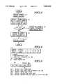
- FIG. 1illustrates, in a block diagram form, a data processing system in accordance with the present invention
- FIG. 2illustrates, in a block diagram form, another data processing system in accordance with the present invention
- FIG. 3illustrates, in a flow chart, a method for providing memory access control in accordance with the present invention
- FIG. 4illustrates, in a block diagram form, a bit configuration of a transparent translation register (TTR) in accordance with the present invention
- FIG. 5illustrates, in a block diagram form, a bit configuration of a default attribute storage register in accordance with the present invention.
- the present inventionprovides a method and an apparatus for providing memory access control within a data processor. This is accomplished by performing a default address mapping of a logical address to a physical address during a normal memory access.
- the methodbegins by providing a privilege mode (supervisor or user) and a logical address to a memory management unit (MMU).
- MMUmemory management unit
- a determination as to whether or not the privilege mode and the logical address match either the privilege mode and a block of logical addresses defined by a first transparent translation register (TTR) or the privilege mode and the block of logical addresses defined by a second transparent translation registeris performed.
- TTRtransparent translation register
- a transparent mapping of the logical address during the memory accessis performed by the first TTR if the first TTR is matched.
- the transparent mapping of the logical addressis performed by the second TTR. However, if neither TTR is matched, a default address translation is invoked and a set of access control bits stored in a default access control register are used for the access.
- the default access control registerprovides write protection via the storing of a write protection bit.
- the default access control registeroutputs attribute bits independent or without considering whether the user or supervisor mode is being utilized. Furthermore, the default access control register outputs attribute bits which may be altered or programmed by a system user or programmer.
- FIG. 1illustrates a system having a processor 10.
- the processor 10has a pipeline unit 12 and a memory management unit (MMU) 14.
- MMUmemory management unit
- Unit 12is used to execute instructions within the processor 10.
- Unit 12operates in one of two levels of privilege: supervisor mode or user mode.
- the processor 10may either be or include a microprocessor, a pipelined execution device, an application specific integrated circuit (ASIC) device, a programmable logic array (PLA), hard-wired logic, an execution unit at least partially software driven by microcode and/or nanocode, a plurality of execution devices, a digital signal processor (DSP), a computer, a data processor, a central processing unit (CPU), a microcontroller unit (MCU) and/or the like.
- ASICapplication specific integrated circuit
- PDAprogrammable logic array
- DSPdigital signal processor
- CPUcentral processing unit
- MCUmicrocontroller unit
- the principal function of MMU 14, within the processor 10,is to translate logical addresses provided by unit 12 to physical addresses using the translation circuitry in a normal mode of operation.
- the translation circuitry 11may require address translation cache (ATC) accesses and/or tablewalks to perform the address translation in the normal mode of operation.
- ATCaddress translation cache
- the translation circuitry 11provides the logical address as the physical address (i.e. logical address bits equal the physical address bits) and the bus attribute bits are derived via circuitry illustrated in FIG. 1.
- the MMU 14operates in one of two modes of operation: normal mode or default mode.
- the MMU 14has a first transparent translation register (TTR) 16 and a second transparent translation register 18 which are used to define blocks of logical addresses to be used as physical addresses during normal memory accesses in the default or normal mode of operation.
- TTRsare usually disabled during the normal mode of operation, in a preferred form, and therefore only used in a default mode of operation.
- the MMU 14also has a page address translation unit which is used to translate logical addresses to physical addresses, which is illustrated in FIG. 1 via the circuitry 11.
- the units 12 and 14are connected to an external memory 26 via an external address bus.
- a bi-directional data busis connected between the external memory 26 and the pipeline unit 12 as illustrated in FIG. 1.
- the address bus and data busgo through logic such as input drivers, output driver I/O drivers, bus control circuitry, cache units, and the like which are not illustrated in FIG. 1 for simplicity.
- Unit 14is also connected to the external memory 26 via a plurality of attribute signals.
- the pipeline unit 12receives data from the memory 26 and the unit 14 provides address and access control information to the memory 26.
- the pipeline unit 12determines that an access to memory 26 is required.
- An internal logical addressis provided to the MMU 14 as illustrated.
- the MMU 14first compares the privilege mode and the logical address, via a comparator unit 20, to the privilege mode and a block of logical addresses defined by TTR 16 and to the privilege mode and the block of logical addresses defined by TTR 18.
- unit 20is a parallel compare unit, although many serial compare units exist in the art and may be used with TTR 16 and TTR 18. If either TTR 16 or TTR 18 is matched via the comparator unit 20, the logical address is used as a physical address for the memory access.
- a multiplexer (MUX) 24which is controlled by the output of the comparator unit 20, passes the set of access control attribute bits stored in the matched TTR (either TTR 16 or TTR 18) to the memory 26 via a plurality of attribute data lines.
- the page address translation unit 11is invoked to perform a physical address translation of the logical address and the output of the MUX 24 is ignored for the memory access. If neither TTR is matched, and the MMU 14 is operating in the default mode, the set of access control bits stored in a programmer visible default access control register 22 is used for the access.
- the external memory 26provides a plurality of data bits to the pipeline unit 12 via the data bus in response to the external physical address.
- the set of access control attribute bits stored in TTR 16, TTR 18, and the default access control register (default storage) 22comprise a set of cache mode bits, a set of user page attribute bits, and a data write access protection bit. It is important to note that if the default access control register 22 did not exist, and the MMU 14 is operating in the default mode, flexible access control could not be provided over the unmapped space in the event of a TTR miss (i.e. no address hit in either TTR 16 or TTR 18). It is also important to note that if the default access control register 22 did not exist, and the MMU 14 is operating in the default mode, data write access protection could not be provided over the unmapped space in the event of a TTR miss.
- FIG. 2illustrates another data processing system having a processor 28 which is connected to an external memory 26 via a plurality of address and data lines.
- the processor 28has a pipeline unit 12 and two independent memory cache units: an instruction cache unit (ICU) 48 and an operand data cache unit (OCU) 66.
- Unit 12is used to execute instructions within the processor 28 and operates in one of two levels of privilege: supervisor mode or user mode.
- the ICU 48 and the OCU 66are connected to unit 12 via a plurality of address and data lines.
- the ICU 48is used to retain copies of recently prefetched instruction data for quick access by the pipeline unit 12.
- the OCU 66is used to retain copies of recently fetched operand data for quick access by the pipeline unit 12.
- ICU 48 and the OCU 66Data stored in the ICU 48 and the OCU 66 can be provided to unit 12, simultaneously, and faster than it can be provided by the external memory 26. Therefore, ICU 48 and OCU 66 are used for the purpose of throughput improvement of instruction data and operand data accesses.
- Processor 28also has a first transparent translation register (TTR) 34 and a second transparent translation register 36 which are used to define blocks of logical addresses to be used as physical addresses during the prefetching of instruction data, and a third transparent translation register 54 and a fourth transparent translation register 56 which are used to define blocks of logical addresses to be used as physical addresses during operand data accesses.
- TTR 34, 36, 54, and 56comprises a logical address base field, a logical address mask field, a privilege mode bit, and a plurality of access control attribute bits which include a set of cache mode bits, a set of user page attribute bits, and a data write access protection bit.
- the pipeline unit 12determines that an instruction data access and/or an operand data access to the ICU 48 and/or the OCU 58 is required. If an instruction data access is required, a logical address 32 (divided into upper and lower bit portions) is provided to the ICU 48 and a comparator circuit 42. The logical address 32 is divided into an upper portion and a lower portion as illustrated. The comparator circuit 42 is used to compare the privilege mode and the upper portion of the logical address to the privilege mode bit and the logical address base bits stored in TTR 34 and to the privilege mode bit and the logical address base bits stored in TTR 36. A mask circuit 38 uses the logical address mask bits stored in TTR 34 to determine which bits of the logical address base field of TTR 34 are ignored during the comparison.
- TTR 34If a logical address mask bit in TTR 34 is set, the corresponding logical address base bit in TTR 34 is ignored during the comparison.
- the mask circuit 40uses the logical address mask bits stored in TTR 36 to determine which bits of the logical address base field of TTR 36 are ignored during the comparison. If either TTR 34 or TTR 36 is matched a selector circuit 44, which is controlled by the output of the comparator circuit 42, passes the set of access control attribute bits stored in the matched TTR to the ICU 48 via a plurality of data lines. If neither TTR is matched, the selector circuit 44 passes the set of access control bits 46a stored in a programmer visible default access control register 46 to the ICU 48.
- the ICU 48searches for cache data within its memory banks in response to the physical address. If found, the ICU 48 supplies the data to the pipeline unit 12 via a plurality of data lines. If the data is not found within the ICU 48, the ICU 48 requests an external memory access and passes the access control attribute bits to the external memory 26 via a plurality of data lines.
- a logical address 52is provided to the OCU 66 and the comparator circuit 62.
- the logical address 52is divided into a similar manner to the logical address 32.
- the comparator circuit 62is used to compare the privilege mode and the upper portion of the logical address to the privilege mode bit and the logical address base bits stored in TTR 54 and to the privilege mode bit and the logical address base bits stored in TTR 56.
- a mask circuit 58uses the logical address mask bits stored in TTR 54 to determine which bits of the logical address base field of TTR 54 are ignored during the comparison. If a logical address mask bit in TTR 54 is set, the corresponding logical address base bit in TTR 54 is ignored during the comparison.
- the mask circuit 60uses the logical address mask bits stored in TTR 56 to determine which bits of the logical address base field of TTR 56 are ignored during the comparison. If either TTR 54 or TTR 56 is matched a selector circuit 64, which is controlled by the output of the comparator circuit 62, passes the set of access control attribute bits stored in the matched TTR to the OCU 66 via a plurality of data lines. If neither TTR is matched, the selector circuit 64 passes a set of access control bits 46b stored in the programmer visible default access control register 46 to the OCU 66. Using the logical address as a physical address, the OCU 66 searches for cache data within its memory banks in response to the physical address.
- the OCU 66supplies the data to the pipeline unit 12 via a plurality of data lines. If the data is not found within the OCU 66, the OCU 66 requests an external memory access and passes the access control attribute bits to the external memory 26 via a plurality of data lines.
- the external memory 26provides a plurality of data bits to the unit 12 via a data bus in response to the physical address.
- the default access control register 46contains a write protection bit, is accessed independent of the user or supervisor mode, and is programmable and therefore very flexible.
- FIG. 3illustrates a flowchart which describes a method used by the processors 10 and/or 28 to provide memory access control.
- a step 100indicates that the pipeline unit 12 is processing an instruction in one of two privilege modes (supervisor or user), needs to perform a normal memory access, and provides a logical address to the MMU 14 and/or the comparator circuits 42 and 62.
- a step 102indicates that the privilege mode and the upper portion of the logical address (see logical addresses 32 and 52 of FIG. 2) are compared, via the compare unit 20 or compare units 42 and 62, to the privilege modes and the blocks of logical address defined by the TTRs 16 and 18 or TTRs 34, 36, 54, and 56.
- a step 104indicates that the MUX 24 or the selector circuits 44 and 64 determine, based on the results from the comparisons performed in step 102, which set of access control attribute bits should be used for the access. Step 104 also implies that the MMU 14 is operating in the default mode. If a TTR miss is detected in step 104, then a step 106 is performed. In step 106, the MUX 24 selects a set of access control attribute bits stored in a default access control register 22. If a TTR hit is detected in step 104, in a step 108 the MUX 24 selects the set of access control attribute bits stored in the matching TTR for the access. In a step 110, the MUX 24 supplies the selected attributes to an external memory 26 and the memory access is completed.
- FIG. 4illustrated a preferred bit format used in FIGS. 1-3 for the TTRs 16, 18, 34, 36, 54, and 56.
- FIG. 4illustrates a transparent translation register (TTR) (preferably having 32 bits) which has several bit fields and bit values described below:
- LOGICAL ADDRESS BASEThis 8-bit field is compared with the eight higher-order bits of the logical address during the privilege mode and logical address comparison and is utilized in the MMU default mode of operation.
- LOGICAL ADDRESS MASKThis 8-bit field is used as a mask for the logical address base field. When a bit in this field is set, the corresponding bit in the logical address base field is ignored during the privilege mode and logical address comparison.
- E--ENABLEThis bit enables and/or disables the TTR register. A disabled TTR is completely ignored during the privilege mode and logical address comparison in the MMU default mode.
- S--SUPERVISOR/USER MODEThis field specifies the privilege mode to be matched during the privilege mode and logical address comparison.
- U--USER PAGE ATTRIBUTES U1, U0These bits are not interpreted by the processor 10 and/or 28 but are echoed to a UPA1 pin and a UPA0 pin on the processor 10 and/or 28 during a normal memory access, respectively.
- the UPA1may be used as a chip select in some designs.
- CM--CACHE MODEThis 2-bit field is used to select the cache mode for a normal memory access.
- the CM fieldallows for four states wherein one state is a cacheable writethrough state, a second state is a cacheable copyback state, a third state is a cache inhibited state, precise exception model, and a fourth state is a cache inhibited state, imprecise exception model.
- W--WRITE PROTECTThis bit indicates if a memory address space is write protected. If set, write and read-modify-write accesses are not permitted to all addresses within the protected address space.
- FIG. 5illustrates a preferred bit format used in FIGS. 1-3 for the default bit portions 44a and 44b in FIG. 2. These bits are described below:
- DCO--DEFAULT OPERAND CACHE MODEThis 2bit field functions in a similar manner to the CM field of the TTR of FIG. 4.
- This 2-bit fieldfunctions in a similar manner to the U1 and U0 bits in the TTR of FIG. 4.
- DCI--DEFAULT INSTRUCTION CACHE MODEThis 2-bit field functions in a similar manner to the DCO field.
- W--WRITE PROTECTThis bit functions in a similar manner to the W bit in the TTR of FIG. 4.
- the present inventionprovides a method and apparatus for providing memory access control in a data processing system. With such a method and apparatus, the flexible default address mapping of a logical address to a physical address can be provided.
- the invention described heremay be compared to other known and documented methods of providing a default address mapping of a logical address to a physical address.
- the default access control attributes bitsare stored in separate registers wherein one register is used for user accesses only and the other register is used for supervisor accesses only.
- the problem with this methodis that it requires the segmenting of the logical address space into supervisor and user spaces, since otherwise, the supervisor space cannot be protected from unauthorized accesses by user programs.
- the inventionsolves this problem by disregarding the privilege mode in providing the default address mapping for a given memory access. Therefore, the integrated circuit used less substrate surface area and speed is improved.
- optional write access protectionis also provided.
- MMU'sfor which the present invention may provide a default address mapping capability, exist in the art wherein the MMU may contain any number of the following: a page address translation cache (ATC), a block address translation cache, a transparent translation register or any other type of address translation facility.
- Bus bit sizesmay vary depending on design constraints.
- bit fields and control signals described hereinmay be either a single bit or a plurality of bits. Zero, one, or more caches may be used in a system.
- Many different methods of encoding and decoding logical addressesexist in the art and all may be used herein as a logical address. It is understood, therefore, that this invention is not limited to the particular forms shown and that it is intended in the appended claims to cover all modifications that do not depart from the spirit and scope of this invention.
Landscapes
- Engineering & Computer Science (AREA)
- Theoretical Computer Science (AREA)
- Physics & Mathematics (AREA)
- General Engineering & Computer Science (AREA)
- General Physics & Mathematics (AREA)
- Computer Security & Cryptography (AREA)
- Storage Device Security (AREA)
- Memory System Of A Hierarchy Structure (AREA)
- Memory System (AREA)
Abstract
Description
Claims (13)
Priority Applications (4)
| Application Number | Priority Date | Filing Date | Title |
|---|---|---|---|
| US08/149,496US5623636A (en) | 1993-11-09 | 1993-11-09 | Data processing system and method for providing memory access protection using transparent translation registers and default attribute bits |
| KR1019940027822AKR100338446B1 (en) | 1993-11-09 | 1994-10-28 | Methods and data processing systems that provide memory access control |
| EP94117230AEP0656592B1 (en) | 1993-11-09 | 1994-11-02 | Memory access control for implementing protected memory regions |
| JP6293671AJPH07191903A (en) | 1993-11-09 | 1994-11-04 | System and operating method of data processing |
Applications Claiming Priority (1)
| Application Number | Priority Date | Filing Date | Title |
|---|---|---|---|
| US08/149,496US5623636A (en) | 1993-11-09 | 1993-11-09 | Data processing system and method for providing memory access protection using transparent translation registers and default attribute bits |
Publications (1)
| Publication Number | Publication Date |
|---|---|
| US5623636Atrue US5623636A (en) | 1997-04-22 |
Family
ID=22530550
Family Applications (1)
| Application Number | Title | Priority Date | Filing Date |
|---|---|---|---|
| US08/149,496Expired - Fee RelatedUS5623636A (en) | 1993-11-09 | 1993-11-09 | Data processing system and method for providing memory access protection using transparent translation registers and default attribute bits |
Country Status (4)
| Country | Link |
|---|---|
| US (1) | US5623636A (en) |
| EP (1) | EP0656592B1 (en) |
| JP (1) | JPH07191903A (en) |
| KR (1) | KR100338446B1 (en) |
Cited By (21)
| Publication number | Priority date | Publication date | Assignee | Title |
|---|---|---|---|---|
| US5842225A (en)* | 1995-02-27 | 1998-11-24 | Sun Microsystems, Inc. | Method and apparatus for implementing non-faulting load instruction |
| US5987557A (en)* | 1997-06-19 | 1999-11-16 | Sun Microsystems, Inc. | Method and apparatus for implementing hardware protection domains in a system with no memory management unit (MMU) |
| US6154818A (en)* | 1997-11-20 | 2000-11-28 | Advanced Micro Devices, Inc. | System and method of controlling access to privilege partitioned address space for a model specific register file |
| WO2001006372A1 (en)* | 1999-07-15 | 2001-01-25 | 3Com Corporation | No stall read access for hiding latency |
| US6321276B1 (en)* | 1998-08-04 | 2001-11-20 | Microsoft Corporation | Recoverable methods and systems for processing input/output requests including virtual memory addresses |
| US6516395B1 (en) | 1997-11-20 | 2003-02-04 | Advanced Micro Devices, Inc. | System and method for controlling access to a privilege-partitioned address space with a fixed set of attributes |
| US6594701B1 (en) | 1998-08-04 | 2003-07-15 | Microsoft Corporation | Credit-based methods and systems for controlling data flow between a sender and a receiver with reduced copying of data |
| US6629187B1 (en)* | 2000-02-18 | 2003-09-30 | Texas Instruments Incorporated | Cache memory controlled by system address properties |
| US20060070077A1 (en)* | 2004-09-30 | 2006-03-30 | Microsoft Corporation | Providing custom product support for a software program |
| US7181600B1 (en)* | 2001-08-02 | 2007-02-20 | Mips Technologies, Inc. | Read-only access to CPO registers |
| US20070043974A1 (en)* | 2005-08-17 | 2007-02-22 | Microsoft Corporation | Techniques for performing memory diagnostics |
| US7185183B1 (en) | 2001-08-02 | 2007-02-27 | Mips Technologies, Inc. | Atomic update of CPO state |
| US20070234020A1 (en)* | 2002-10-22 | 2007-10-04 | Mips Technologies, Inc. | Instruction encoding for system register bit set and clear |
| CN100426264C (en)* | 2005-10-19 | 2008-10-15 | 联发科技股份有限公司 | Method for accessing memory and related microprocessor system |
| US20140068158A1 (en)* | 2012-09-05 | 2014-03-06 | Silicon Motion, Inc. | Flash storage device and control method for flash memory |
| US8817571B2 (en) | 2010-05-12 | 2014-08-26 | Samsung Electronics Co., Ltd. | Semiconductor memory device and semiconductor memory system |
| JP2015060499A (en)* | 2013-09-20 | 2015-03-30 | 富士通株式会社 | Arithmetic processing device, information processing device, control method for information processing device, and control program for information processing device |
| US9367309B2 (en) | 2013-09-24 | 2016-06-14 | Apple Inc. | Predicate attribute tracker |
| US9390058B2 (en) | 2013-09-24 | 2016-07-12 | Apple Inc. | Dynamic attribute inference |
| CN108959110A (en)* | 2011-12-29 | 2018-12-07 | 英特尔公司 | Administrator mode executes protection |
| WO2019182855A1 (en)* | 2018-03-23 | 2019-09-26 | Intel Corporation | Systems, methods, and apparatuses for defending against cross-privilege linear probes |
Families Citing this family (11)
| Publication number | Priority date | Publication date | Assignee | Title |
|---|---|---|---|---|
| JP3082701B2 (en)* | 1997-03-14 | 2000-08-28 | 日本電気株式会社 | Memory protection device and memory protection method |
| GB2325061B (en)* | 1997-04-30 | 2001-06-06 | Advanced Risc Mach Ltd | Memory access protection |
| US6233667B1 (en) | 1999-03-05 | 2001-05-15 | Sun Microsystems, Inc. | Method and apparatus for a high-performance embedded memory management unit |
| US6754784B1 (en)* | 2000-02-01 | 2004-06-22 | Cirrus Logic, Inc. | Methods and circuits for securing encached information |
| US10409614B2 (en) | 2017-04-24 | 2019-09-10 | Intel Corporation | Instructions having support for floating point and integer data types in the same register |
| US10474458B2 (en) | 2017-04-28 | 2019-11-12 | Intel Corporation | Instructions and logic to perform floating-point and integer operations for machine learning |
| CN113383310A (en) | 2019-03-15 | 2021-09-10 | 英特尔公司 | Pulse decomposition within matrix accelerator architecture |
| US11934342B2 (en) | 2019-03-15 | 2024-03-19 | Intel Corporation | Assistance for hardware prefetch in cache access |
| EP3938913A1 (en)* | 2019-03-15 | 2022-01-19 | INTEL Corporation | Multi-tile architecture for graphics operations |
| EP3938893B1 (en) | 2019-03-15 | 2025-10-15 | Intel Corporation | Systems and methods for cache optimization |
| US11663746B2 (en) | 2019-11-15 | 2023-05-30 | Intel Corporation | Systolic arithmetic on sparse data |
Citations (4)
| Publication number | Priority date | Publication date | Assignee | Title |
|---|---|---|---|---|
| WO1988002148A1 (en)* | 1986-09-15 | 1988-03-24 | Motorola, Inc. | A transparent translation method and apparatus for use in a memory management unit |
| US5091846A (en)* | 1986-10-03 | 1992-02-25 | Intergraph Corporation | Cache providing caching/non-caching write-through and copyback modes for virtual addresses and including bus snooping to maintain coherency |
| GB2248327A (en)* | 1990-08-31 | 1992-04-01 | Hitachi Ltd | Fixed protection key for real storage memory |
| US5321836A (en)* | 1985-06-13 | 1994-06-14 | Intel Corporation | Virtual memory management method and apparatus utilizing separate and independent segmentation and paging mechanism |
Family Cites Families (3)
| Publication number | Priority date | Publication date | Assignee | Title |
|---|---|---|---|---|
| US4763250A (en)* | 1985-04-01 | 1988-08-09 | Motorola, Inc. | Paged memory management unit having variable number of translation table levels |
| US5075846A (en)* | 1989-09-29 | 1991-12-24 | Motorola, Inc. | Memory access serialization as an MMU page attribute |
| US5278961A (en)* | 1990-02-22 | 1994-01-11 | Hewlett-Packard Company | Physical address to logical address translator for memory management units |
- 1993
- 1993-11-09USUS08/149,496patent/US5623636A/ennot_activeExpired - Fee Related
- 1994
- 1994-10-28KRKR1019940027822Apatent/KR100338446B1/ennot_activeExpired - Fee Related
- 1994-11-02EPEP94117230Apatent/EP0656592B1/ennot_activeExpired - Lifetime
- 1994-11-04JPJP6293671Apatent/JPH07191903A/enactivePending
Patent Citations (4)
| Publication number | Priority date | Publication date | Assignee | Title |
|---|---|---|---|---|
| US5321836A (en)* | 1985-06-13 | 1994-06-14 | Intel Corporation | Virtual memory management method and apparatus utilizing separate and independent segmentation and paging mechanism |
| WO1988002148A1 (en)* | 1986-09-15 | 1988-03-24 | Motorola, Inc. | A transparent translation method and apparatus for use in a memory management unit |
| US5091846A (en)* | 1986-10-03 | 1992-02-25 | Intergraph Corporation | Cache providing caching/non-caching write-through and copyback modes for virtual addresses and including bus snooping to maintain coherency |
| GB2248327A (en)* | 1990-08-31 | 1992-04-01 | Hitachi Ltd | Fixed protection key for real storage memory |
Cited By (30)
| Publication number | Priority date | Publication date | Assignee | Title |
|---|---|---|---|---|
| US5842225A (en)* | 1995-02-27 | 1998-11-24 | Sun Microsystems, Inc. | Method and apparatus for implementing non-faulting load instruction |
| US5987557A (en)* | 1997-06-19 | 1999-11-16 | Sun Microsystems, Inc. | Method and apparatus for implementing hardware protection domains in a system with no memory management unit (MMU) |
| US6154818A (en)* | 1997-11-20 | 2000-11-28 | Advanced Micro Devices, Inc. | System and method of controlling access to privilege partitioned address space for a model specific register file |
| US6516395B1 (en) | 1997-11-20 | 2003-02-04 | Advanced Micro Devices, Inc. | System and method for controlling access to a privilege-partitioned address space with a fixed set of attributes |
| US6321276B1 (en)* | 1998-08-04 | 2001-11-20 | Microsoft Corporation | Recoverable methods and systems for processing input/output requests including virtual memory addresses |
| US6594701B1 (en) | 1998-08-04 | 2003-07-15 | Microsoft Corporation | Credit-based methods and systems for controlling data flow between a sender and a receiver with reduced copying of data |
| US6760787B2 (en) | 1998-08-04 | 2004-07-06 | Miscrosoft Corporation | Recoverable methods and systems for processing input/output requests including virtual memory addresses |
| WO2001006372A1 (en)* | 1999-07-15 | 2001-01-25 | 3Com Corporation | No stall read access for hiding latency |
| US6282626B1 (en)* | 1999-07-15 | 2001-08-28 | 3Com Corporation | No stall read access-method for hiding latency in processor memory accesses |
| US6629187B1 (en)* | 2000-02-18 | 2003-09-30 | Texas Instruments Incorporated | Cache memory controlled by system address properties |
| US7185183B1 (en) | 2001-08-02 | 2007-02-27 | Mips Technologies, Inc. | Atomic update of CPO state |
| US7181600B1 (en)* | 2001-08-02 | 2007-02-20 | Mips Technologies, Inc. | Read-only access to CPO registers |
| US20070234020A1 (en)* | 2002-10-22 | 2007-10-04 | Mips Technologies, Inc. | Instruction encoding for system register bit set and clear |
| US7600100B2 (en) | 2002-10-22 | 2009-10-06 | Mips Technologies, Inc. | Instruction encoding for system register bit set and clear |
| US7634638B1 (en) | 2002-10-22 | 2009-12-15 | Mips Technologies, Inc. | Instruction encoding for system register bit set and clear |
| US20100031005A1 (en)* | 2002-10-22 | 2010-02-04 | Mips Technologies, Inc. | Instruction Encoding For System Register Bit Set And Clear |
| US20060070077A1 (en)* | 2004-09-30 | 2006-03-30 | Microsoft Corporation | Providing custom product support for a software program |
| US20070043974A1 (en)* | 2005-08-17 | 2007-02-22 | Microsoft Corporation | Techniques for performing memory diagnostics |
| US7818625B2 (en)* | 2005-08-17 | 2010-10-19 | Microsoft Corporation | Techniques for performing memory diagnostics |
| CN100426264C (en)* | 2005-10-19 | 2008-10-15 | 联发科技股份有限公司 | Method for accessing memory and related microprocessor system |
| US8817571B2 (en) | 2010-05-12 | 2014-08-26 | Samsung Electronics Co., Ltd. | Semiconductor memory device and semiconductor memory system |
| CN108959110A (en)* | 2011-12-29 | 2018-12-07 | 英特尔公司 | Administrator mode executes protection |
| CN108959110B (en)* | 2011-12-29 | 2023-05-30 | 太浩研究有限公司 | Processor for preventing administrator mode execution of user mode instructions and method thereof |
| US20140068158A1 (en)* | 2012-09-05 | 2014-03-06 | Silicon Motion, Inc. | Flash storage device and control method for flash memory |
| US9563550B2 (en)* | 2012-09-05 | 2017-02-07 | Silicon Motion, Inc. | Flash storage device and control method for flash memory |
| JP2015060499A (en)* | 2013-09-20 | 2015-03-30 | 富士通株式会社 | Arithmetic processing device, information processing device, control method for information processing device, and control program for information processing device |
| US9367309B2 (en) | 2013-09-24 | 2016-06-14 | Apple Inc. | Predicate attribute tracker |
| US9390058B2 (en) | 2013-09-24 | 2016-07-12 | Apple Inc. | Dynamic attribute inference |
| WO2019182855A1 (en)* | 2018-03-23 | 2019-09-26 | Intel Corporation | Systems, methods, and apparatuses for defending against cross-privilege linear probes |
| US10831679B2 (en) | 2018-03-23 | 2020-11-10 | Intel Corporation | Systems, methods, and apparatuses for defending against cross-privilege linear probes |
Also Published As
| Publication number | Publication date |
|---|---|
| EP0656592B1 (en) | 1998-10-21 |
| EP0656592A1 (en) | 1995-06-07 |
| KR100338446B1 (en) | 2002-09-27 |
| KR950015083A (en) | 1995-06-16 |
| JPH07191903A (en) | 1995-07-28 |
Similar Documents
| Publication | Publication Date | Title |
|---|---|---|
| US5623636A (en) | Data processing system and method for providing memory access protection using transparent translation registers and default attribute bits | |
| US7401358B1 (en) | Method of controlling access to control registers of a microprocessor | |
| US7043616B1 (en) | Method of controlling access to model specific registers of a microprocessor | |
| US5909696A (en) | Method and apparatus for caching system management mode information with other information | |
| US4800489A (en) | Paged memory management unit capable of selectively supporting multiple address spaces | |
| US5247639A (en) | Microprocessor having cache bypass signal terminal | |
| US5325499A (en) | Computer system including a write protection circuit for preventing illegal write operations and a write poster with improved memory | |
| US5854913A (en) | Microprocessor with an architecture mode control capable of supporting extensions of two distinct instruction-set architectures | |
| US6266755B1 (en) | Translation lookaside buffer with virtual address conflict prevention | |
| US6397301B1 (en) | Preventing access to secure area of a cache | |
| US8051301B2 (en) | Memory management system and method providing linear address based memory access security | |
| US4763250A (en) | Paged memory management unit having variable number of translation table levels | |
| US6233667B1 (en) | Method and apparatus for a high-performance embedded memory management unit | |
| US5940858A (en) | Cache circuit with programmable sizing and method of operation | |
| US7082507B1 (en) | Method of controlling access to an address translation data structure of a computer system | |
| EP1490774A1 (en) | System and method providing region-granular, hardware-controlled memory encryption | |
| US6351797B1 (en) | Translation look-aside buffer for storing region configuration bits and method of operation | |
| US5497458A (en) | Cache testability circuit for embedded diagnostics | |
| US7146477B1 (en) | Mechanism for selectively blocking peripheral device accesses to system memory | |
| US6938127B2 (en) | Reconfiguring memory to reduce boot time | |
| WO2003050688A2 (en) | System and method for handling device accesses to a memory providing increased memory access security | |
| US7634635B1 (en) | Systems and methods for reordering processor instructions | |
| US5954812A (en) | Apparatus for caching system management memory in a computer having a system management mode employing address translation | |
| US5732405A (en) | Method and apparatus for performing a cache operation in a data processing system | |
| US5860096A (en) | Multi-level instruction cache for a computer |
Legal Events
| Date | Code | Title | Description |
|---|---|---|---|
| AS | Assignment | Owner name:MOTOROLA, INC., ILLINOIS Free format text:ASSIGNMENT OF ASSIGNORS INTEREST;ASSIGNOR:REVILLA, JUAN G.;REEL/FRAME:006776/0947 Effective date:19931104 Owner name:MOTOROLA, INC., ILLINOIS Free format text:ASSIGNMENT OF ASSIGNORS INTEREST;ASSIGNOR:PARMET, ART;REEL/FRAME:006776/0944 Effective date:19931103 | |
| FPAY | Fee payment | Year of fee payment:4 | |
| AS | Assignment | Owner name:FREESCALE SEMICONDUCTOR, INC., TEXAS Free format text:ASSIGNMENT OF ASSIGNORS INTEREST;ASSIGNOR:MOTOROLA, INC.;REEL/FRAME:015698/0657 Effective date:20040404 Owner name:FREESCALE SEMICONDUCTOR, INC.,TEXAS Free format text:ASSIGNMENT OF ASSIGNORS INTEREST;ASSIGNOR:MOTOROLA, INC.;REEL/FRAME:015698/0657 Effective date:20040404 | |
| REMI | Maintenance fee reminder mailed | ||
| LAPS | Lapse for failure to pay maintenance fees | ||
| STCH | Information on status: patent discontinuation | Free format text:PATENT EXPIRED DUE TO NONPAYMENT OF MAINTENANCE FEES UNDER 37 CFR 1.362 | |
| FP | Expired due to failure to pay maintenance fee | Effective date:20050422 |