US5623213A - Membrane probing of circuits - Google Patents
Membrane probing of circuitsDownload PDFInfo
- Publication number
- US5623213A US5623213AUS08/643,740US64374096AUS5623213AUS 5623213 AUS5623213 AUS 5623213AUS 64374096 AUS64374096 AUS 64374096AUS 5623213 AUS5623213 AUS 5623213A
- Authority
- US
- United States
- Prior art keywords
- bump
- bumps
- substrate
- conductive
- pads
- Prior art date
- Legal status (The legal status is an assumption and is not a legal conclusion. Google has not performed a legal analysis and makes no representation as to the accuracy of the status listed.)
- Expired - Fee Related
Links
Images


Classifications
- G—PHYSICS
- G01—MEASURING; TESTING
- G01R—MEASURING ELECTRIC VARIABLES; MEASURING MAGNETIC VARIABLES
- G01R1/00—Details of instruments or arrangements of the types included in groups G01R5/00 - G01R13/00 and G01R31/00
- G01R1/02—General constructional details
- G01R1/06—Measuring leads; Measuring probes
- G01R1/067—Measuring probes
- G01R1/073—Multiple probes
- G01R1/07307—Multiple probes with individual probe elements, e.g. needles, cantilever beams or bump contacts, fixed in relation to each other, e.g. bed of nails fixture or probe card
- G01R1/0735—Multiple probes with individual probe elements, e.g. needles, cantilever beams or bump contacts, fixed in relation to each other, e.g. bed of nails fixture or probe card arranged on a flexible frame or film
Definitions
- This inventionrelates to membrane probing of circuits.
- Circuits to be probedmay include those which are formed as part of "dice” arranged in rows and columns on a silicon wafer during the process of making integrated circuits (IC's).
- Each dieincludes as many as a hundred or more aluminum input/output (I/O) pads for connecting the circuit on the die to the outside world.
- the padsare typically tiny and closely spaced, e.g., on the order of 100 microns center-to-center (pitch).
- the performance and/or integrity of the dice circuitsmay be tested before the dice are cut out of the wafer and packaged. Testing is typically done by conductive probes that make physical and electrical contact with the die pads. Generally, the probes are either hard pins (e.g., tungsten), or hard bumps formed on a membrane surface. The close spacing of the die pads requires that the probes be carefully aligned, often by hand or by using a special visual alignment system. During testing, the probes are forced into contact with the pads.
- the sharp probe tipsare wiped across the pads to abrade or scratch a thin layer of insulating aluminum oxide (which sometimes forms on the pads), thus exposing non-oxidized portions of the pads. Because the probe tips become dirty from this and other processes, they are periodically cleaned with an abrasive such as sandpaper.
- the probesrelay the appropriate power, data, and other signals between the die and a tester.
- the frequency at which these test signals are communicatedis determined at least in part by the inductance of the probes and the impedance of the electrical interconnections between the die and the tester.
- first and second bumps electrically connected at first and second positions along a conductive run borne by a flexible substrateare respectively oriented for contact with a pad of a die under test and a pad of a tester structure.
- the two bumpsmay be manufactured using the same process, and at the same time.
- An electrical connection between the first bump and the tester structuremay be made by forcing the second bump into contact with the tester structure pad.
- the conductive runneed not be soldered or otherwise hard-wired to the tester structure, reducing the expense and difficulty of electrically interfacing the substrate and the tester structure.
- the substrate, and in particular the second bumpmay be releasably attached to the tester structure, allowing the substrate to be easily and rapidly removed. Thus, should either of the bumps wear out, the substrate may be quickly replaced.
- a die having a different pad arrangementmay be tested using the same tester structure by substituting a substrate having a suitably oriented first bump.
- Embodiments of the inventionmay include the following features. Groups of first and second bumps interconnected by conductive runs may be respectively oriented for contact with corresponding groups of die and tester structure pads.
- the bumpswhich may be exposed on the same surface of the substrate, may be plated with hard particles to penetrate aluminum oxide accumulations on the surfaces of the die and tester structure pads.
- the first group of bumpsmay be on a portion of the substrate that spans an open region enclosed by a first frame bonded to a center region of the substrate.
- the second group of bumpsmay be on a portion of the substrate that spans an open region enclosed by a second frame bonded to an end of the substrate.
- a releasable attachment mechanism coupling the second frame to the tester structuremay include a spring and a cushion (e.g., a layer of rubber between a layer of substantially rigid material and a layer of Kapton), both of which are between the substrate and a plate.
- Forcing the plate towards the tester structureapplies a distributed load across the substrate surface so that all of the second bumps contact their respective tester structure pads with about the same force.
- the substratehas a U-shaped cross-section.
- second and third conductive regionsare electrically connected respectively to the power and ground terminals of a power source and an electrical device.
- the second and third regionsare spaced from a first conductive region to filter high-frequency noise components from power and ground potentials provided by the power source.
- this aspect of the inventionfilters or attenuates high frequency noise that might otherwise interfere with the proper operation of the electrical device from the nominally constant power and ground potentials provided by the power source.
- Embodiments of the inventionmay include the following features.
- the second and third regionsmay be parallel to, and spaced an identical distance from a surface of, the first region, which is electrically connected to a system ground. Insulating material (e.g., polyimide) between the first region and each of the second and third regions may help maintain the proper spacing between the regions.
- Insulating materiale.g., polyimide
- the first, second and third regionsall have substantially uniform thicknesses.
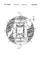
- FIG. 1ais a cross-sectional view of a testing apparatus.
- FIG. 1bis another cross-sectional view of the testing apparatus, taken along a section line perpendicular to the section line of the view shown in FIG. 1a.
- FIG. 1cis a top view of the testing apparatus.
- FIG. 1dis a cross-sectional view of another testing apparatus.
- FIGS. 2-4are perspectives top, and sectional (taken along line 4--4 in FIG. 3) views, respectively, of a membrane probe card of the testing apparatus of FIGS. 1a, 1b, and 1c.
- FIG. 5is a cross-sectional view of a portion of a membrane of the membrane probe card.
- FIG. 6is a bottom view of a membrane assembly of the membrane probe card.
- FIG. 7is a top view of the membrane assembly.
- FIG. 8is a cross-sectional view, not to scale, of a membrane assembly at an intermediate stage of manufacture.
- FIG. 9is a top view of a printed circuit board of the membrane probe card.
- FIGS. 10 and 11are broken-away top and sectional views (taken along line 11--11 in FIG. 10), respectively, of a mechanism for attaching the membrane assembly to the printed circuit board.
- FIG. 12is a schematic illustration of the Vcc, Vss, and Vref regions of the membrane assembly and the printed circuit board connected to power supply power, power supply ground, and system ground, respectively.
- a testing apparatus 1 for testing dice on a silicon wafer 2includes a membrane assembly 3 and a pressure mechanism 4, both attached to a printed circuit board (PCB) 5 (PCB 5 is not shown in FIG. 1c). Screws 6 attach PCB 5 to a housing 7. Pressure mechanism 4 maintains a suitable contact force between the pads 8 of a die (not shown) on wafer 2 and conductive bumps 9 (e.g., of nickel, gold, or copper) exposed on a membrane 10 of membrane assembly 3. Bumps 9, which are arranged in accordance with the locations of the pads 8 of the die under test, electrically connect to a tester (not shown). Wafer 2 is held fixed by a vacuum chuck 11.
- PCB 5printed circuit board
- vacuum chuck 11Prior to testing, vacuum chuck 11 is moved laterally with respect to membrane 10 to align die pads 8 under membrane bumps 9. When wafer 2 and membrane 10 are properly oriented, vacuum chuck 11 is then moved vertically with respect to PCB 5, forcing die pads 8 into mechanical and electrical contact with bumps 9. The tester can then exchange signals with, provide power to, and evaluate the performance of, the die.
- Pressure mechanism 4includes a pusher 12 connected, through a ball-and-socket joint 13, to the base of a threaded rod 14.
- Sleeves 15a, 15bthread onto rod 14, and attach at the centers of belleville springs 16a, 16b.
- Belleville springs 16a, 16bare substantially umbrella-shaped--round when viewed from the top (FIG. 1c), and frusto-conical when viewed from the sides.
- the periphery of each spring 16a, 16battaches to a support block 17. Screws 18 attach flanges 19 of support block 17 to PCB 5.
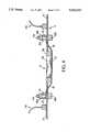
- FIG. 1dAn alternate pressure mechanism 22 for use with a similar membrane assembly 23 is shown in FIG. 1d.
- a support block 24 in pressure mechanism 22houses an expandable fluid chamber 25.
- Membrane assembly 23is attached to the bottom surface of support block 24, and a pushing plate 26 on the bottom of fluid chamber 25 contacts the back side of membrane assembly 23 in the region of bumps 30.
- Valved lines 27, 28supply fluid (e.g., liquid or gas) to and withdraw fluid from chamber 25.
- a CPUmonitors the signal generated by a pressure transducer 29 in fluid communication with chamber 25, opening and closing the valves in lines 27, 28 to maintain the desired pressure level in chamber 25.
- the CPUPrior to testing, the CPU reduces the pressure in chamber 25 to essentially zero. Wafer 2 is then moved vertically until die pads 8 are close to, but not touching, membrane bumps 30 of membrane assembly 23. The pressure in chamber 25 is then increased to some predetermined level, forcing bumps 30 into contact with pads 8. As this occurs, rigid pushing plate 26 rotates, allowing bumps 30 to orient parallel to wafer 2 so that all of bumps 30 may come into contact with pads 8.
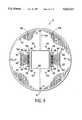
- membrane assembly 3comprises membrane 10, a square probe frame 32 bonded at the center of membrane 10, and a pair of rectangular connector frames 34 bonded at opposite ends of membrane 10.
- Four holes 42one in each corner of probe frame 32, accept screws 21 (FIGS. 1a and 1b) for attaching probe frame 32 to support block 17 of pressure mechanism 4.
- Probe frame 32encloses an open region 33, spanned by membrane 10 like a drum head.
- Connector frames 34likewise enclose open regions 35, spanned by membrane 10.
- the bottom surfaces of bumps 9 of membrane 10are plated with particles 44.
- Particles 44comprised, e.g., of nickel coated with gold or rhodium, are relatively hard and angular, with sharp points suitable for penetrating aluminum oxide accumulations on the surface of the die pads.
- Bumps 9attach to bump pads 46 on the bottom surface of membrane 10, and thus bumps 9 are exposed on the bottom surface of membrane 10.
- Bump pads 46are electrically insulated from a signal and reference layer 48 by a bottom dielectric layer 50.
- the conductive portions of signal and reference layer 48are formed, in a manner described below, from a 4 micron copper sheet.
- Dielectric layer 50is a 10 micron layer of a polymer such as polyimide.
- Signal and reference layer 48includes signal runs 52, which electrically interconnect with bump pads 46 through conductive vias 54 passing through bottom dielectric layer 50. Signal runs 52 are generally between 16 and 20 microns wide.
- a middle dielectric layer 56e.g., a 10-20 micron polyimide layer
- a top dielectric layer 60e.g., a 10 micron polyimide layer is located on top of power and ground layer 58.
- bump pads 46are grouped on the portion of membrane 10 that spans open region 33 of probe frame 32.
- bump pads 46are arranged to correspond to pads 8 of the die to be tested in apparatus 1.
- Two other sets of bump pads 62, 63are arranged, in 3 pad ⁇ 30 pad matrices, on the portion of membrane 10 that spans open regions 35 of connector frames 34.
- Each signal run 52extends from a point directly above a bump pad 46 within the center region of probe frame 32 to a point directly above a bump pad 62, 63 within the center region of one of connector frames 34. (For clarity, signal runs 52 are shown solid--not in phantom--in FIG. 6, although it can be seen from FIG.
- a via(not shown in FIG. 6) at each end of each signal run 52 connects the signal runs to the corresponding bump pad 46, 62, 63 located directly below.
- a conductive Vref region 64flanks signal runs 52 in layer 48. (For clarity, Vref region 64 is shown solid--not in phantom--in FIG. 6, although Vref region 64 lies in the same plane as signal runs 52). Vias (not shown in FIG. 6) connect Vref region 64 to the bump pads 62, 63 located directly below it. Thus, as shown in FIG. 6, each end 65a, 65b, 65c, 65d of each portion 67a, 67b of Vref region 64 connects to the nine bump pads 62, 63 located directly below it. Also as shown in FIG. 6, holes 42 are countersunk or chamfered on the bottom surface of membrane assembly 3.
- power and ground layer 58includes a rectangular conductive Vcc region 66 that extends across approximately half the length of power and ground layer 58, and a conductive Vss region 68 that extends across approximately the other half of the length of power and ground layer 58.
- Vcc region 66 and Vss region 68together occupy substantially all of power and ground layer 58. Because of their proximity, Vref region 64 and Vcc region 66 together comprise as a capacitor, as do Vref region 64 and Vss region 68.
- Vias(not shown in FIG. 7) connect Vcc region 66 and Vss region 68 to the respective bump pads 62, 63 located directly below it that are not otherwise connected to either Vref region 64 or a signal run 52.
- Another viaconnects Vcc region 66 to a bump pad 71, the associated bump 9 of which is oriented to contact the power pad of the die under test.
- Vss region 68is likewise connected to a bump pad 72, the associated bump 9 of which is oriented to contact the ground pad of the die under test.
- polyimide layer 60is first formed, using conventional techniques, on the bottom surface of a solid substrate, such as a 0.050 in. thick aluminum wafer 73. As described below, probe frame 32 and connector frames 34 are formed from aluminum wafer 73. In this manner, polyimide layer 60 forms a durable mechanical bond with the surface of aluminum wafer 73. Power and ground layer 58 is then formed by sputtering a 4 micron copper layer onto the exposed surface of layer 60, and then using photo lithography to remove the unwanted conductive material to form Vcc region 66 and Vss region 68. Polyimide layers 50, 56, signal and reference plane 48, vias 54, and bump pads 46 are formed using similar conventional techniques. Bumps 9 are then grown at the desired locations on bump pads 46 and plated with particles 44, such as in the manner described in U.S. Pat. Nos. 4,804,132 and 5,083,697, incorporated herein by reference.
- membrane 10When membrane 10 is completely formed, the bottom surface of membrane 10 is covered with either or both pressure sensitive tape or photoresist. This protects membrane 10, and in particular bumps 9 and particles 44, from mechanical abrasion or chemical attack during the subsequent manufacturing steps.
- attachment holes 42 and alignment holes 75are drilled through aluminum wafer 73.
- Recesses 76, 78, 80, 82, 84are then mechanically machined into the top surface of aluminum wafer 73.
- Recesses 76, 84correspond to the openings in connector frames 34
- recess 80corresponds to the opening in probe frame 32.
- Recesses 78, 82correspond to the gaps between connector frames 34 and probe frame 32.
- Recesses 76, 78, 80, 82, 84are machined until they extend about 80% of the way through aluminum wafer 73. Thus, for a 0.050 in. substrate, the recesses are machined to a depth of about 0.040 in.
- MillingAny number of methods can be used to machine recesses 76, 78, 80, 82, 84. Milling, high-speed routing, electro-discharge machining (EDM), or beadblasting through a mask are all viable techniques, depending on precision and cost constraints.
- EDMelectro-discharge machining
- the recessesare chemically etched to remove the remaining 20% of the aluminum substrate material, exposing the top surface of membrane 10. Any number of chemical etchants may be used, as long as the polyimide layer 60 is not chemically attacked by it.
- the etchant temperatureis carefully controlled to provide a constant etch rate. Because only 20% of the substrate material is removed by etching, the etchant does not substantially undercut the remaining substrate material, even when an isotropic etchant is used.
- PCB 5shown approximately to scale in FIG. 9, includes four alignment pins 86 sized and located to seat in alignment holes 75 in connector frames 34. Disposed between alignment pins 86, and adjacent to hole 38, are two 3 ⁇ 30 matrices of pads 88, 89. Pads 88, 89 are arranged to correspond to bump pads 62, 63 of membrane assembly 3 (FIG. 6). With connector frames 34 mechanically attached to PCB 5, as described below in connection with FIGS. 10 and 11, the membrane bumps 9 associated with bump pads 62 make contact with pads 88, and the membrane bumps 9 associated with bump pads 63 make contact with pads 89 (FIGS.
- Membrane bumps 9, and the particles 44 plated thereuponpenetrate aluminum oxide accumulations on the surface of pads 88, 89, facilitating the electrical interconnection between bump pads 62, 63 and respective pads 88, 89.
- pads 88, 89are electrically interfaced with pads 62, 63 of membrane assembly 3.
- An insulating materialcovers the bottom surface of PCB Vref region 91.
- pads 88, 89 that interface with bump pads 62, 63 connected to Vcc region 66 and Vss region 68electrically connect through vias to a conductive PCB Vcc region 98 and a conductive PCB Vss region 100, respectively.
- PCB Vcc region 98 and PCB Vss region 100together cover substantially the entire top surface of PCB 5.
- PCB Vref region 91 and PCB Vcc region 98together serve as a capacitor, as do PCB Vref region 91 and PCB Vss region 100.
- a pad 104electrically connects to PCB Vcc region 98, a pad 105 electrically connects to PCB Vss region 100, and pads 107 electrically connects to PCB Vref region 91.
- pads 88, 89 that interface with bump pads 62, 63 connected to signal runs 52electrically connect through conductive PCB runs 90 to pads 92.
- An insulting material disposed on the top surface of PCB Vss region 100 and PCB Vcc region 98insulates PCB runs 90 from PCB Vss region 100 and PCB Vcc region 98.
- a connector block/ribbon cable assembly 94(shown in FIGS. 2-4) electrically connects to each set of pads 92, as well as to pads 104, 105, 107, relaying power, data, and other signals between PCB 5 and the tester.
- pad 104(which electrically connects to Vcc regions 66, 98 of both PCB 5 and installed membrane assembly 3) is connected to the positive terminal of a power supply (not shown) in the tester.
- Pad 105(which electrically connects to Vss regions 68, 100 of both PCB 5 and installed membrane assembly 3) is connected to the negative terminal of the power supply in the tester.
- Pad 107(which electrically connects to Vref regions 64, 91 of both PCB 5 and installed membrane assembly 3) is connected to the system, or chassis, ground of the tester.
- the lateral alignment of bump pads 62, 63 with respect to pads 88, 89is maintained by alignment pins 86 in PCB 5, which seat in alignment holes 75 of connector frames 34.
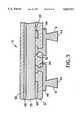
- connector frame 34 and PCB 5are sandwiched between a top pressure plate 106 and a bottom pressure plate 108, both of which are constructed of a rigid material such as stainless steel.
- Pressure springs 110 and a pressure uniformity cushion 112are disposed between membrane 10 and top pressure plate 106.
- Cushion 112includes a compliant layer 111 (e.g., rubber) sandwiched between a stainless steel layer 113 and a layer of plastic material 115 (e.g., Kapton).
- Cushion 112rests in opening 76 in connector frame 34 (see FIG. 8), with stainless steel layer 113 disposed adjacent to springs 110, and Kapton layer 115 disposed adjacent to the top surface of membrane 10. As pressure screws 114 (which pass through holes 116 in PCB 5) are tightened, pressure plates 106, 108 are drawn closer together. The resultant loading is distributed evenly by springs 110 and pressure uniformity cushion 112 over the surface of membrane 10, ensuring that bumps 9 engage pads 88, 96, 104 with substantially uniform force.
- membrane assembly 3can be replaced with a fresh assembly by simply disassembling the releasable attachment mechanism shown in FIGS. 10 and 11, removing the spent assembly, orienting a fresh membrane on alignment pins 86 at the edges of hole 38, and reassembling the mechanism.
- vacuum chuck 11is activated to hold wafer 2 fixed. Vacuum chuck 11 is then moved laterally with respect to membrane 10 to align the die pads with the membrane bumps 9. With the die pads properly oriented, vacuum chuck 11 is moved vertically to force the die pads into electrical contact with bumps 9, providing a plurality of continuous current flow paths between the die pads and the tester electrically connected to connector block/ribbon cable assembly 94.
- Activating the testersupplies power, typically +5 volts DC (VDC), to Vcc regions 66, 98 (and thus pad 71) through pad 104.
- VDCvoltage
- Vss regions 68, 100 (and thus pad 72) and Vref regions 68, 91are electrically connected to power supply ground (i.e., 0 VDC) and system ground through pads 105 and 107, respectively.
- the testersupplies test signals to the die, generally at high frequency to increase the die testing rate.
- the resultant high-frequency switching of transistors in the diecauses corresponding high-frequency, low-amplitude fluctuations in the power demanded by the die.
- Vref regions 68, 91, Vcc regions 66, 98, and Vss regions 68, 100serve as series capacitor networks between Vcc and Vss, as illustrated schematically in FIG. 12, these fluctuations in power demand do not result in substantial fluctuations in the Vcc and Vss voltage levels.
- the arrangement of the conductive Vcc, Vss, and Vref regions ACcouples the Vcc and Vss regions to one another, serving to filter or attenuate high frequency noise from the otherwise nominally constant power and ground signals.
- membrane assembly 3has been shown and described as attached to a printed circuit board, any suitable interface structure, such as a frame or other fixture, may be used.
- pressure uniformity cushion 112contacts membrane 10 directly, an attachment mechanism could instead apply force directly to connector frames 34 to force bumps 9 into contact with pads 88, 96, 104 of PCB 5.
- bumps 9need not be plated with particles 44.
Landscapes
- Physics & Mathematics (AREA)
- General Physics & Mathematics (AREA)
- Measuring Leads Or Probes (AREA)
- Testing Or Measuring Of Semiconductors Or The Like (AREA)
Abstract
Description
Claims (12)
Priority Applications (2)
| Application Number | Priority Date | Filing Date | Title |
|---|---|---|---|
| US08/643,740US5623213A (en) | 1994-09-09 | 1996-05-06 | Membrane probing of circuits |
| US08/764,511US5841291A (en) | 1994-09-09 | 1996-12-12 | Exchangeable membrane probe testing of circuits |
Applications Claiming Priority (2)
| Application Number | Priority Date | Filing Date | Title |
|---|---|---|---|
| US30349894A | 1994-09-09 | 1994-09-09 | |
| US08/643,740US5623213A (en) | 1994-09-09 | 1996-05-06 | Membrane probing of circuits |
Related Parent Applications (1)
| Application Number | Title | Priority Date | Filing Date |
|---|---|---|---|
| US30349894AContinuation | 1994-09-09 | 1994-09-09 |
Related Child Applications (1)
| Application Number | Title | Priority Date | Filing Date |
|---|---|---|---|
| US08/764,511DivisionUS5841291A (en) | 1994-09-09 | 1996-12-12 | Exchangeable membrane probe testing of circuits |
Publications (1)
| Publication Number | Publication Date |
|---|---|
| US5623213Atrue US5623213A (en) | 1997-04-22 |
Family
ID=23172391
Family Applications (2)
| Application Number | Title | Priority Date | Filing Date |
|---|---|---|---|
| US08/643,740Expired - Fee RelatedUS5623213A (en) | 1994-09-09 | 1996-05-06 | Membrane probing of circuits |
| US08/764,511Expired - Fee RelatedUS5841291A (en) | 1994-09-09 | 1996-12-12 | Exchangeable membrane probe testing of circuits |
Family Applications After (1)
| Application Number | Title | Priority Date | Filing Date |
|---|---|---|---|
| US08/764,511Expired - Fee RelatedUS5841291A (en) | 1994-09-09 | 1996-12-12 | Exchangeable membrane probe testing of circuits |
Country Status (4)
| Country | Link |
|---|---|
| US (2) | US5623213A (en) |
| EP (1) | EP0779989A4 (en) |
| JP (1) | JPH10505162A (en) |
| WO (1) | WO1996007924A1 (en) |
Cited By (58)
| Publication number | Priority date | Publication date | Assignee | Title |
|---|---|---|---|---|
| WO1999005701A3 (en)* | 1997-07-22 | 1999-04-15 | Dytak Corp | Composite electrical contact structure and method for manufacturing the same |
| US5914613A (en)* | 1996-08-08 | 1999-06-22 | Cascade Microtech, Inc. | Membrane probing system with local contact scrub |
| US5968282A (en)* | 1997-11-10 | 1999-10-19 | Tokyo Electron Limited | Mechanism and method for cleaning probe needles |
| US6246245B1 (en)* | 1998-02-23 | 2001-06-12 | Micron Technology, Inc. | Probe card, test method and test system for semiconductor wafers |
| US6256882B1 (en) | 1998-07-14 | 2001-07-10 | Cascade Microtech, Inc. | Membrane probing system |
| US6499216B1 (en) | 1994-07-07 | 2002-12-31 | Tessera, Inc. | Methods and structures for electronic probing arrays |
| US6566898B2 (en) | 2000-03-06 | 2003-05-20 | Wentworth Laboratories, Inc. | Temperature compensated vertical pin probing device |
| US20030101584A1 (en)* | 1998-06-09 | 2003-06-05 | Shigeru Matsumura | Bump and method of forming bump |
| US6578264B1 (en) | 1999-06-04 | 2003-06-17 | Cascade Microtech, Inc. | Method for constructing a membrane probe using a depression |
| US6586955B2 (en) | 2000-03-13 | 2003-07-01 | Tessera, Inc. | Methods and structures for electronic probing arrays |
| US20030132767A1 (en)* | 2000-02-25 | 2003-07-17 | Tervo Paul A. | Membrane probing system |
| US6633175B1 (en) | 2000-03-06 | 2003-10-14 | Wenworth Laboratories, Inc. | Temperature compensated vertical pin probing device |
| US20030199179A1 (en)* | 1993-11-16 | 2003-10-23 | Formfactor, Inc. | Contact tip structure for microelectronic interconnection elements and method of making same |
| US6661244B2 (en) | 2000-03-06 | 2003-12-09 | Wentworth Laboratories, Inc. | Nickel alloy probe card frame laminate |
| US6690186B2 (en) | 1994-07-07 | 2004-02-10 | Tessera, Inc. | Methods and structures for electronic probing arrays |
| US20040036493A1 (en)* | 2002-05-08 | 2004-02-26 | Miller Charles A. | High performance probe system |
| US20040046579A1 (en)* | 2002-05-08 | 2004-03-11 | Formfactor, Inc. | High performance probe system |
| US20040051546A1 (en)* | 2000-03-06 | 2004-03-18 | Wentworth Laboratories, Inc. | Temperature compensated vertical pin probing device |
| US6756797B2 (en) | 2001-01-31 | 2004-06-29 | Wentworth Laboratories Inc. | Planarizing interposer for thermal compensation of a probe card |
| US7161363B2 (en) | 2002-05-23 | 2007-01-09 | Cascade Microtech, Inc. | Probe for testing a device under test |
| US20070013408A1 (en)* | 2005-07-13 | 2007-01-18 | Agilent Technologies, Inc. | Inspection device for display panel and interface used therein |
| US20070075717A1 (en)* | 2005-09-14 | 2007-04-05 | Touchdown Technologies, Inc. | Lateral interposer contact design and probe card assembly |
| US7233160B2 (en) | 2000-12-04 | 2007-06-19 | Cascade Microtech, Inc. | Wafer probe |
| US7271603B2 (en) | 2003-05-23 | 2007-09-18 | Cascade Microtech, Inc. | Shielded probe for testing a device under test |
| US7285969B2 (en) | 2002-11-13 | 2007-10-23 | Cascade Microtech, Inc. | Probe for combined signals |
| US20070268035A1 (en)* | 2006-05-19 | 2007-11-22 | Elpida Memory, Inc. | Probe card |
| US7355420B2 (en)* | 2001-08-21 | 2008-04-08 | Cascade Microtech, Inc. | Membrane probing system |
| US7368927B2 (en) | 2004-07-07 | 2008-05-06 | Cascade Microtech, Inc. | Probe head having a membrane suspended probe |
| US7403028B2 (en) | 2006-06-12 | 2008-07-22 | Cascade Microtech, Inc. | Test structure and probe for differential signals |
| US7420381B2 (en) | 2004-09-13 | 2008-09-02 | Cascade Microtech, Inc. | Double sided probing structures |
| US7427868B2 (en) | 2003-12-24 | 2008-09-23 | Cascade Microtech, Inc. | Active wafer probe |
| US7443186B2 (en) | 2006-06-12 | 2008-10-28 | Cascade Microtech, Inc. | On-wafer test structures for differential signals |
| US7449899B2 (en) | 2005-06-08 | 2008-11-11 | Cascade Microtech, Inc. | Probe for high frequency signals |
| US7504842B2 (en) | 1997-05-28 | 2009-03-17 | Cascade Microtech, Inc. | Probe holder for testing of a test device |
| US7535247B2 (en) | 2005-01-31 | 2009-05-19 | Cascade Microtech, Inc. | Interface for testing semiconductors |
| US20090146675A1 (en)* | 2007-12-10 | 2009-06-11 | Touchdown Technologies, Inc. | Planarizing probe card |
| US7601039B2 (en) | 1993-11-16 | 2009-10-13 | Formfactor, Inc. | Microelectronic contact structure and method of making same |
| US20090264025A1 (en)* | 2006-04-14 | 2009-10-22 | Kabushiki Kaisha Nihon Micronics | Probe sheet and electrical connecting apparatus |
| US7609077B2 (en) | 2006-06-09 | 2009-10-27 | Cascade Microtech, Inc. | Differential signal probe with integral balun |
| US7619419B2 (en) | 2005-06-13 | 2009-11-17 | Cascade Microtech, Inc. | Wideband active-passive differential signal probe |
| US7656172B2 (en) | 2005-01-31 | 2010-02-02 | Cascade Microtech, Inc. | System for testing semiconductors |
| US20100029099A1 (en)* | 2006-04-07 | 2010-02-04 | Kabushiki Kaisha Nihon Micronics | Electrical connecting apparatus |
| US20100105224A1 (en)* | 2006-09-28 | 2010-04-29 | Kabushiki Kaisha Nihon Micronics | Electrical connecting apparatus |
| US7723999B2 (en) | 2006-06-12 | 2010-05-25 | Cascade Microtech, Inc. | Calibration structures for differential signal probing |
| US7764072B2 (en) | 2006-06-12 | 2010-07-27 | Cascade Microtech, Inc. | Differential signal probing system |
| US7876114B2 (en) | 2007-08-08 | 2011-01-25 | Cascade Microtech, Inc. | Differential waveguide probe |
| US7888957B2 (en) | 2008-10-06 | 2011-02-15 | Cascade Microtech, Inc. | Probing apparatus with impedance optimized interface |
| US20110159444A1 (en)* | 2006-04-14 | 2011-06-30 | Kabushiki Kaisha Nihon Micronics | Method for manufacturing probe sheet |
| US8033838B2 (en) | 1996-02-21 | 2011-10-11 | Formfactor, Inc. | Microelectronic contact structure |
| US8373428B2 (en) | 1993-11-16 | 2013-02-12 | Formfactor, Inc. | Probe card assembly and kit, and methods of making same |
| US8410806B2 (en) | 2008-11-21 | 2013-04-02 | Cascade Microtech, Inc. | Replaceable coupon for a probing apparatus |
| US9435855B2 (en) | 2013-11-19 | 2016-09-06 | Teradyne, Inc. | Interconnect for transmitting signals between a device and a tester |
| US9594114B2 (en) | 2014-06-26 | 2017-03-14 | Teradyne, Inc. | Structure for transmitting signals in an application space between a device under test and test electronics |
| US9977052B2 (en) | 2016-10-04 | 2018-05-22 | Teradyne, Inc. | Test fixture |
| US10677815B2 (en) | 2018-06-08 | 2020-06-09 | Teradyne, Inc. | Test system having distributed resources |
| US11002763B2 (en) | 2018-08-10 | 2021-05-11 | Globalfoundries U.S. Inc. | Probe for pic die with related test assembly and method |
| US11363746B2 (en) | 2019-09-06 | 2022-06-14 | Teradyne, Inc. | EMI shielding for a signal trace |
| US11862901B2 (en) | 2020-12-15 | 2024-01-02 | Teradyne, Inc. | Interposer |
Families Citing this family (14)
| Publication number | Priority date | Publication date | Assignee | Title |
|---|---|---|---|---|
| US5491651A (en)* | 1992-05-15 | 1996-02-13 | Key, Idea Development | Flexible wearable computer |
| JP2001506779A (en)* | 1996-11-01 | 2001-05-22 | ヴィーア・インコーポレイテッド | Flexible wearable computer system |
| US6060891A (en)* | 1997-02-11 | 2000-05-09 | Micron Technology, Inc. | Probe card for semiconductor wafers and method and system for testing wafers |
| JPH1123615A (en) | 1997-05-09 | 1999-01-29 | Hitachi Ltd | Connection device and inspection system |
| JP3324741B2 (en)* | 1997-10-14 | 2002-09-17 | 矢崎総業株式会社 | Device and method for measuring displacement of elastic contact piece of terminal |
| TW508440B (en)* | 1999-12-27 | 2002-11-01 | Hoya Co Ltd | Probe structure and manufacturing method thereof |
| AU5935001A (en)* | 2000-05-02 | 2001-11-12 | Thomas Distefano | Connector apparatus |
| US6426638B1 (en)* | 2000-05-02 | 2002-07-30 | Decision Track Llc | Compliant probe apparatus |
| US6577147B2 (en) | 2001-09-06 | 2003-06-10 | Intel Corporation | Method and apparatus for resisting probe burn using shape memory alloy probe during testing of an electronic device |
| US7694246B2 (en)* | 2002-06-19 | 2010-04-06 | Formfactor, Inc. | Test method for yielding a known good die |
| US7382143B2 (en)* | 2006-05-18 | 2008-06-03 | Centipede Systems, Inc. | Wafer probe interconnect system |
| US7442045B1 (en) | 2007-08-17 | 2008-10-28 | Centipede Systems, Inc. | Miniature electrical ball and tube socket with self-capturing multiple-contact-point coupling |
| US7579850B2 (en)* | 2007-08-23 | 2009-08-25 | Allstron Inc. | Probe card and method for assembling the same |
| US9702906B2 (en)* | 2015-06-26 | 2017-07-11 | International Business Machines Corporation | Non-permanent termination structure for microprobe measurements |
Citations (36)
| Publication number | Priority date | Publication date | Assignee | Title |
|---|---|---|---|---|
| US3516077A (en)* | 1968-05-28 | 1970-06-02 | Bell Telephone Labor Inc | Magnetic propagation device wherein pole patterns move along the periphery of magnetic disks |
| US3577131A (en)* | 1969-01-30 | 1971-05-04 | Bell Telephone Labor Inc | Domain propagation arrangement |
| US3673433A (en)* | 1970-08-21 | 1972-06-27 | Siemens Ag Albis | Circuit arrangement for selectively connecting at least two inputs to a counting stage possessing at least one preparatory input and one triggering input and including contact bounce suppression circuitry |
| US3934236A (en)* | 1974-01-11 | 1976-01-20 | Monsanto Company | Pulsed field accessed bubble propagation circuits |
| US4021790A (en)* | 1974-01-11 | 1977-05-03 | Monsanto Company | Mutually exclusive magnetic bubble propagation circuits |
| US4117543A (en)* | 1972-08-24 | 1978-09-26 | Monsanto Company | Magnetic bubble logic family |
| US4692839A (en)* | 1985-06-24 | 1987-09-08 | Digital Equipment Corporation | Multiple chip interconnection system and package |
| US4729166A (en)* | 1985-07-22 | 1988-03-08 | Digital Equipment Corporation | Method of fabricating electrical connector for surface mounting |
| US4754546A (en)* | 1985-07-22 | 1988-07-05 | Digital Equipment Corporation | Electrical connector for surface mounting and method of making thereof |
| US4757256A (en)* | 1985-05-10 | 1988-07-12 | Micro-Probe, Inc. | High density probe card |
| US4758785A (en)* | 1986-09-03 | 1988-07-19 | Tektronix, Inc. | Pressure control apparatus for use in an integrated circuit testing station |
| WO1988005544A1 (en)* | 1987-01-20 | 1988-07-28 | Hughes Aircraft Company | Test connector for electrical devices |
| US4778950A (en)* | 1985-07-22 | 1988-10-18 | Digital Equipment Corporation | Anisotropic elastomeric interconnecting system |
| EP0298219A2 (en)* | 1987-06-08 | 1989-01-11 | Tektronix Inc. | Method and apparatus for testing unpackaged integrated circuits in a hybrid circuit environment |
| US4804132A (en)* | 1987-08-28 | 1989-02-14 | Difrancesco Louis | Method for cold bonding |
| US4912399A (en)* | 1987-06-09 | 1990-03-27 | Tektronix, Inc. | Multiple lead probe for integrated circuits in wafer form |
| EP0361779A1 (en)* | 1988-09-26 | 1990-04-04 | Hewlett-Packard Company | Micro-strip architecture for membrane test probe |
| US4918383A (en)* | 1987-01-20 | 1990-04-17 | Huff Richard E | Membrane probe with automatic contact scrub action |
| US4922192A (en)* | 1988-09-06 | 1990-05-01 | Unisys Corporation | Elastic membrane probe |
| US4954873A (en)* | 1985-07-22 | 1990-09-04 | Digital Equipment Corporation | Electrical connector for surface mounting |
| US4975638A (en)* | 1989-12-18 | 1990-12-04 | Wentworth Laboratories | Test probe assembly for testing integrated circuit devices |
| US4980637A (en)* | 1988-03-01 | 1990-12-25 | Hewlett-Packard Company | Force delivery system for improved precision membrane probe |
| US5020219A (en)* | 1988-05-16 | 1991-06-04 | Leedy Glenn J | Method of making a flexible tester surface for testing integrated circuits |
| US5072176A (en)* | 1990-07-10 | 1991-12-10 | The United States Of America As Represented By The Secretary Of The Army | Flexible membrane circuit tester |
| US5083697A (en)* | 1990-02-14 | 1992-01-28 | Difrancesco Louis | Particle-enhanced joining of metal surfaces |
| US5103557A (en)* | 1988-05-16 | 1992-04-14 | Leedy Glenn J | Making and testing an integrated circuit using high density probe points |
| US5132613A (en)* | 1990-11-30 | 1992-07-21 | International Business Machines Corporation | Low inductance side mount decoupling test structure |
| US5180977A (en)* | 1991-12-02 | 1993-01-19 | Hoya Corporation Usa | Membrane probe contact bump compliancy system |
| US5264787A (en)* | 1991-08-30 | 1993-11-23 | Hughes Aircraft Company | Rigid-flex circuits with raised features as IC test probes |
| US5355079A (en)* | 1993-01-07 | 1994-10-11 | Wentworth Laboratories, Inc. | Probe assembly for testing integrated circuit devices |
| US5378982A (en)* | 1993-02-25 | 1995-01-03 | Hughes Aircraft Company | Test probe for panel having an overlying protective member adjacent panel contacts |
| US5416429A (en)* | 1994-05-23 | 1995-05-16 | Wentworth Laboratories, Inc. | Probe assembly for testing integrated circuits |
| US5422574A (en)* | 1993-01-14 | 1995-06-06 | Probe Technology Corporation | Large scale protrusion membrane for semiconductor devices under test with very high pin counts |
| US5456404A (en)* | 1993-10-28 | 1995-10-10 | Digital Equipment Corporation | Method of testing semiconductor chips with reusable test package |
| US5468157A (en)* | 1993-10-29 | 1995-11-21 | Texas Instruments Incorporated | Non-destructive interconnect system for semiconductor devices |
| US5469072A (en)* | 1993-11-01 | 1995-11-21 | Motorola, Inc. | Integrated circuit test system |
Family Cites Families (5)
| Publication number | Priority date | Publication date | Assignee | Title |
|---|---|---|---|---|
| US3963986A (en)* | 1975-02-10 | 1976-06-15 | International Business Machines Corporation | Programmable interface contactor structure |
| US4835464A (en)* | 1987-04-23 | 1989-05-30 | Micro Component Technology, Inc. | Decoupling apparatus for use with integrated circuit tester |
| US5068602A (en)* | 1990-09-07 | 1991-11-26 | Tektronix, Inc. | DUT board for a semiconductor device tester having a reconfigurable coaxial interconnect grid and method of using same |
| US5502397A (en)* | 1992-11-12 | 1996-03-26 | Advanced Micro Devices, Inc. | Integrated circuit testing apparatus and method |
| US5461326A (en)* | 1993-02-25 | 1995-10-24 | Hughes Aircraft Company | Self leveling and self tensioning membrane test probe |
- 1995
- 1995-09-08WOPCT/US1995/011273patent/WO1996007924A1/ennot_activeApplication Discontinuation
- 1995-09-08JPJP8509640Apatent/JPH10505162A/enactivePending
- 1995-09-08EPEP95931069Apatent/EP0779989A4/ennot_activeWithdrawn
- 1996
- 1996-05-06USUS08/643,740patent/US5623213A/ennot_activeExpired - Fee Related
- 1996-12-12USUS08/764,511patent/US5841291A/ennot_activeExpired - Fee Related
Patent Citations (36)
| Publication number | Priority date | Publication date | Assignee | Title |
|---|---|---|---|---|
| US3516077A (en)* | 1968-05-28 | 1970-06-02 | Bell Telephone Labor Inc | Magnetic propagation device wherein pole patterns move along the periphery of magnetic disks |
| US3577131A (en)* | 1969-01-30 | 1971-05-04 | Bell Telephone Labor Inc | Domain propagation arrangement |
| US3673433A (en)* | 1970-08-21 | 1972-06-27 | Siemens Ag Albis | Circuit arrangement for selectively connecting at least two inputs to a counting stage possessing at least one preparatory input and one triggering input and including contact bounce suppression circuitry |
| US4117543A (en)* | 1972-08-24 | 1978-09-26 | Monsanto Company | Magnetic bubble logic family |
| US3934236A (en)* | 1974-01-11 | 1976-01-20 | Monsanto Company | Pulsed field accessed bubble propagation circuits |
| US4021790A (en)* | 1974-01-11 | 1977-05-03 | Monsanto Company | Mutually exclusive magnetic bubble propagation circuits |
| US4757256A (en)* | 1985-05-10 | 1988-07-12 | Micro-Probe, Inc. | High density probe card |
| US4692839A (en)* | 1985-06-24 | 1987-09-08 | Digital Equipment Corporation | Multiple chip interconnection system and package |
| US4778950A (en)* | 1985-07-22 | 1988-10-18 | Digital Equipment Corporation | Anisotropic elastomeric interconnecting system |
| US4729166A (en)* | 1985-07-22 | 1988-03-08 | Digital Equipment Corporation | Method of fabricating electrical connector for surface mounting |
| US4754546A (en)* | 1985-07-22 | 1988-07-05 | Digital Equipment Corporation | Electrical connector for surface mounting and method of making thereof |
| US4954873A (en)* | 1985-07-22 | 1990-09-04 | Digital Equipment Corporation | Electrical connector for surface mounting |
| US4758785A (en)* | 1986-09-03 | 1988-07-19 | Tektronix, Inc. | Pressure control apparatus for use in an integrated circuit testing station |
| US4918383A (en)* | 1987-01-20 | 1990-04-17 | Huff Richard E | Membrane probe with automatic contact scrub action |
| WO1988005544A1 (en)* | 1987-01-20 | 1988-07-28 | Hughes Aircraft Company | Test connector for electrical devices |
| EP0298219A2 (en)* | 1987-06-08 | 1989-01-11 | Tektronix Inc. | Method and apparatus for testing unpackaged integrated circuits in a hybrid circuit environment |
| US4912399A (en)* | 1987-06-09 | 1990-03-27 | Tektronix, Inc. | Multiple lead probe for integrated circuits in wafer form |
| US4804132A (en)* | 1987-08-28 | 1989-02-14 | Difrancesco Louis | Method for cold bonding |
| US4980637A (en)* | 1988-03-01 | 1990-12-25 | Hewlett-Packard Company | Force delivery system for improved precision membrane probe |
| US5103557A (en)* | 1988-05-16 | 1992-04-14 | Leedy Glenn J | Making and testing an integrated circuit using high density probe points |
| US5020219A (en)* | 1988-05-16 | 1991-06-04 | Leedy Glenn J | Method of making a flexible tester surface for testing integrated circuits |
| US4922192A (en)* | 1988-09-06 | 1990-05-01 | Unisys Corporation | Elastic membrane probe |
| EP0361779A1 (en)* | 1988-09-26 | 1990-04-04 | Hewlett-Packard Company | Micro-strip architecture for membrane test probe |
| US4975638A (en)* | 1989-12-18 | 1990-12-04 | Wentworth Laboratories | Test probe assembly for testing integrated circuit devices |
| US5083697A (en)* | 1990-02-14 | 1992-01-28 | Difrancesco Louis | Particle-enhanced joining of metal surfaces |
| US5072176A (en)* | 1990-07-10 | 1991-12-10 | The United States Of America As Represented By The Secretary Of The Army | Flexible membrane circuit tester |
| US5132613A (en)* | 1990-11-30 | 1992-07-21 | International Business Machines Corporation | Low inductance side mount decoupling test structure |
| US5264787A (en)* | 1991-08-30 | 1993-11-23 | Hughes Aircraft Company | Rigid-flex circuits with raised features as IC test probes |
| US5180977A (en)* | 1991-12-02 | 1993-01-19 | Hoya Corporation Usa | Membrane probe contact bump compliancy system |
| US5355079A (en)* | 1993-01-07 | 1994-10-11 | Wentworth Laboratories, Inc. | Probe assembly for testing integrated circuit devices |
| US5422574A (en)* | 1993-01-14 | 1995-06-06 | Probe Technology Corporation | Large scale protrusion membrane for semiconductor devices under test with very high pin counts |
| US5378982A (en)* | 1993-02-25 | 1995-01-03 | Hughes Aircraft Company | Test probe for panel having an overlying protective member adjacent panel contacts |
| US5456404A (en)* | 1993-10-28 | 1995-10-10 | Digital Equipment Corporation | Method of testing semiconductor chips with reusable test package |
| US5468157A (en)* | 1993-10-29 | 1995-11-21 | Texas Instruments Incorporated | Non-destructive interconnect system for semiconductor devices |
| US5469072A (en)* | 1993-11-01 | 1995-11-21 | Motorola, Inc. | Integrated circuit test system |
| US5416429A (en)* | 1994-05-23 | 1995-05-16 | Wentworth Laboratories, Inc. | Probe assembly for testing integrated circuits |
Non-Patent Citations (42)
| Title |
|---|
| Brunner et al., "Electron-Beam MCM Testing and Probing," IEEE Transactions on Components, Packaging, and Manufacturing Technology--Part B: Advanced Packaging (1994). |
| Brunner et al., Electron Beam MCM Testing and Probing, IEEE Transactions on Components, Packaging, and Manufacturing Technology Part B: Advanced Packaging (1994).* |
| Chong et al., "The Evolution of MCM Test from High Performance Bipolar Mainframe Multichip Modules to Low Cost Work Station Multichip Modules," ICEMM Proceedings '93, pp. 404-410 (Month Unavailable). |
| Chong et al., The Evolution of MCM Test from High Performance Bipolar Mainframe Multichip Modules to Low Cost Work Station Multichip Modules, ICEMM Proceedings 93 , pp. 404 410 (Month Unavailable).* |
| Davidson, E., "Design, Analysis, Applications," IEEE Transactions on Components, Packaging, and Manufacturing Technology--Part B: Advanced Packaging (1994) 17(1):2 (Feb. 1994). |
| Davidson, E., Design, Analysis, Applications, IEEE Transactions on Components, Packaging, and Manufacturing Technology Part B: Advanced Packaging (1994) 17(1):2 (Feb. 1994).* |
| Doane, D., "Foreward: Advancing MCM Technnologies," IEEE Transactions on Components, Packaging, and Manufacturing Technology--Part B: Advanced Packaging (1994) 17(1):1 (Feb. 1994). |
| Doane, D., Foreward: Advancing MCM Technnologies, IEEE Transactions on Components, Packaging, and Manufacturing Technology Part B: Advanced Packaging (1994) 17(1):1 (Feb. 1994).* |
| Economikos et al., "Electrical Test of Multichip Substrates," IEEE Transactions on Components, Packaging, and Manufacturing Technology--Part B: Advanced Packaging (1994) 17(1):56-61 (Feb. 1994). |
| Economikos et al., Electrical Test of Multichip Substrates, IEEE Transactions on Components, Packaging, and Manufacturing Technology Part B: Advanced Packaging (1994) 17(1):56 61 (Feb. 1994).* |
| Fisher et al, "Reducing Test Costs for High-Speed and High Pin-Count Devices", Probe Technology, Feb. 1992; Santa Clara, CA. |
| Fisher et al, Reducing Test Costs for High Speed and High Pin Count Devices , Probe Technology , Feb. 1992; Santa Clara, CA.* |
| Fresh Quest Corporation , Fresh Quest Corporation Announces the Deliver of QC 2TM Bare Die Carriers and QPC TM Probe Cards For the Production of Known Good Die ; Chandler, AZ (Date Unavailable).* |
| Fresh Quest Corporation , Quest Pricing Guidelines (Date Unavailable).* |
| Fresh Quest Corporation, "Fresh Quest Corporation Announces the Deliver of QC2TM Bare Die Carriers and QPCTM Probe Cards For the Production of Known Good Die"; Chandler, AZ (Date Unavailable). |
| Fresh Quest Corporation, "Quest Pricing Guidelines" (Date Unavailable). |
| Hewlett Packard , High Speed Wafer Probing with the HP 83000 Model F660 ; 1993; Germany (Month Unavailable).* |
| Hewlett Packard, "High Speed Wafer Probing with the HP 83000 Model F660"; 1993; Germany (Month Unavailable). |
| Hughes , Membrane Wafer Probe The Future of the IC Test Industry (Date Unavailable).* |
| Hughes Aircraft Company , Additional Technical Data for Hughes Membrane Test Probe ; 1993 (Month Unavailable).* |
| Hughes Aircraft Company, "Additional Technical Data for Hughes' Membrane Test Probe"; 1993 (Month Unavailable). |
| Hughes, "Membrane Wafer Probe--The Future of the IC Test Industry" (Date Unavailable). |
| Jensen, R., "Fabrication, Technology," IEEE Transactions on Components, Packaging, and Manufacturing Technology--Part B: Advanced Packaging (1994) 17(1):2 (Feb. 1994). |
| Jensen, R., Fabrication, Technology, IEEE Transactions on Components, Packaging, and Manufacturing Technology Part B: Advanced Packaging (1994) 17(1):2 (Feb. 1994).* |
| Kister et al., "Test Cost Reduction Using the Membrane Probe" [Title Not Legible], Probe Technology; Santa Clara, CA (Date Unavailable). |
| Kister et al., "Test Cost Reduction Using the Membrane Probe", Probe Technology; Santa Clara, CA (Date Unavailable). |
| Kister et al., Test Cost Reduction Using the Membrane Probe , Probe Technology ; Santa Clara, CA (Date Unavailable).* |
| Kister et al., Test Cost Reduction Using the Membrane Probe Title Not Legible , Probe Technology ; Santa Clara, CA (Date Unavailable).* |
| Marshall et al., "CAD-Based Net Capacitance Testing of Unpopulated MCM Substrates," IEEE Transactions on Components, Packaging, and Manufacturing Technology--Part B: Advanced Packaging (1994) 17(1):50-55 (Feb. 1994). |
| Marshall et al., CAD Based Net Capacitance Testing of Unpopulated MCM Substrates, IEEE Transactions on Components, Packaging, and Manufacturing Technology Part B: Advanced Packaging (1994) 17(1):50 55 (Feb. 1994).* |
| Packard Hughes Interconnect , Our New IC Membrane Test Probe. It s Priced the Same, But It Costs Less. , Irvine, CA; 1993 (Month Unavailable).* |
| Packard Hughes Interconnect , Science Over Art, Our New IC Membrane Test Probe ; 1993; Irvine, CA (Month Unavailable).* |
| Packard Hughes Interconnect, "Our New IC Membrane Test Probe. It's Priced the Same, But It Costs Less.", Irvine, CA; 1993 (Month Unavailable). |
| Packard Hughes Interconnect, "Science Over Art, Our New IC Membrane Test Probe"; 1993; Irvine, CA (Month Unavailable). |
| Probe Technology , Membrane Probe Card The Concept (Date Unavailable).* |
| Probe Technology , Prober Interface Unit for HP83000 Model INT768 (Date Unavailable).* |
| Probe Technology, "Membrane Probe Card--The Concept" (Date Unavailable). |
| Probe Technology, "Prober Interface Unit for HP83000 Model - INT768" (Date Unavailable). |
| Russell, T., "Testing," IEEE Transactions on Components, Packaging, and Manufacturing Technology--Part B: Advanced Packaging (1994)17(1):2 (Feb. 1994). |
| Russell, T., Testing, IEEE Transactions on Components, Packaging, and Manufacturing Technology Part B: Advanced Packaging (1994)17(1):2 (Feb. 1994).* |
| West, et al., Principles of CMOS VLSI Design: A Systems Perspective , 2nd Ed., (1993), Chapter 8 (Month Unavailable).* |
| West, et al., Principles of CMOS VLSI Design: A Systems Perspective, 2nd Ed., (1993), Chapter 8 (Month Unavailable). |
Cited By (128)
| Publication number | Priority date | Publication date | Assignee | Title |
|---|---|---|---|---|
| US8373428B2 (en) | 1993-11-16 | 2013-02-12 | Formfactor, Inc. | Probe card assembly and kit, and methods of making same |
| US7601039B2 (en) | 1993-11-16 | 2009-10-13 | Formfactor, Inc. | Microelectronic contact structure and method of making same |
| US20030199179A1 (en)* | 1993-11-16 | 2003-10-23 | Formfactor, Inc. | Contact tip structure for microelectronic interconnection elements and method of making same |
| US6690186B2 (en) | 1994-07-07 | 2004-02-10 | Tessera, Inc. | Methods and structures for electronic probing arrays |
| US6499216B1 (en) | 1994-07-07 | 2002-12-31 | Tessera, Inc. | Methods and structures for electronic probing arrays |
| US8033838B2 (en) | 1996-02-21 | 2011-10-11 | Formfactor, Inc. | Microelectronic contact structure |
| US20020135388A1 (en)* | 1996-08-08 | 2002-09-26 | Gleason K. Reed | Membrane probing system with local contact scrub |
| US7109731B2 (en) | 1996-08-08 | 2006-09-19 | Cascade Microtech, Inc. | Membrane probing system with local contact scrub |
| US5914613A (en)* | 1996-08-08 | 1999-06-22 | Cascade Microtech, Inc. | Membrane probing system with local contact scrub |
| US6437584B1 (en) | 1996-08-08 | 2002-08-20 | Cascade Microtech, Inc. | Membrane probing system with local contact scrub |
| US6307387B1 (en) | 1996-08-08 | 2001-10-23 | Cascade Microtech, Inc. | Membrane probing system with local contact scrub |
| US7893704B2 (en) | 1996-08-08 | 2011-02-22 | Cascade Microtech, Inc. | Membrane probing structure with laterally scrubbing contacts |
| US7541821B2 (en) | 1996-08-08 | 2009-06-02 | Cascade Microtech, Inc. | Membrane probing system with local contact scrub |
| US6927585B2 (en) | 1996-08-08 | 2005-08-09 | Cascade Microtech, Inc. | Membrane probing system with local contact scrub |
| US7504842B2 (en) | 1997-05-28 | 2009-03-17 | Cascade Microtech, Inc. | Probe holder for testing of a test device |
| US5973405A (en)* | 1997-07-22 | 1999-10-26 | Dytak Corporation | Composite electrical contact structure and method for manufacturing the same |
| US6359337B1 (en) | 1997-07-22 | 2002-03-19 | Dytak Corporation | Composite electrical contact structure and method for manufacturing the same |
| WO1999005701A3 (en)* | 1997-07-22 | 1999-04-15 | Dytak Corp | Composite electrical contact structure and method for manufacturing the same |
| US5968282A (en)* | 1997-11-10 | 1999-10-19 | Tokyo Electron Limited | Mechanism and method for cleaning probe needles |
| US6356098B1 (en) | 1998-02-23 | 2002-03-12 | Micron Technology, Inc. | Probe card, test method and test system for semiconductor wafers |
| US6246245B1 (en)* | 1998-02-23 | 2001-06-12 | Micron Technology, Inc. | Probe card, test method and test system for semiconductor wafers |
| US20030101584A1 (en)* | 1998-06-09 | 2003-06-05 | Shigeru Matsumura | Bump and method of forming bump |
| US7084657B2 (en)* | 1998-06-09 | 2006-08-01 | Advantest Corporation | Bump and method of forming bump |
| US7266889B2 (en) | 1998-07-14 | 2007-09-11 | Cascade Microtech, Inc. | Membrane probing system |
| US7761986B2 (en) | 1998-07-14 | 2010-07-27 | Cascade Microtech, Inc. | Membrane probing method using improved contact |
| US6708386B2 (en) | 1998-07-14 | 2004-03-23 | Cascade Microtech, Inc. | Method for probing an electrical device having a layer of oxide thereon |
| US20040093716A1 (en)* | 1998-07-14 | 2004-05-20 | Reed Gleason | Membrane probing system |
| US20100271060A1 (en)* | 1998-07-14 | 2010-10-28 | Cascade Microtech, Inc. | Membrane probing method using improved contact |
| US6825677B2 (en) | 1998-07-14 | 2004-11-30 | Cascade Microtech, Inc. | Membrane probing system |
| US8451017B2 (en)* | 1998-07-14 | 2013-05-28 | Cascade Microtech, Inc. | Membrane probing method using improved contact |
| US6256882B1 (en) | 1998-07-14 | 2001-07-10 | Cascade Microtech, Inc. | Membrane probing system |
| US6860009B2 (en) | 1998-07-14 | 2005-03-01 | Cascade Microtech, Inc. | Probe construction using a recess |
| US7400155B2 (en) | 1998-07-14 | 2008-07-15 | Cascade Microtech, Inc. | Membrane probing system |
| US7681312B2 (en) | 1998-07-14 | 2010-03-23 | Cascade Microtech, Inc. | Membrane probing system |
| US7533462B2 (en) | 1999-06-04 | 2009-05-19 | Cascade Microtech, Inc. | Method of constructing a membrane probe |
| US6578264B1 (en) | 1999-06-04 | 2003-06-17 | Cascade Microtech, Inc. | Method for constructing a membrane probe using a depression |
| US20030192183A1 (en)* | 1999-06-04 | 2003-10-16 | Reed Gleason | Method for constructing a membrane probe using a depression |
| US7178236B2 (en) | 1999-06-04 | 2007-02-20 | Cascade Microtech, Inc. | Method for constructing a membrane probe using a depression |
| US6838890B2 (en) | 2000-02-25 | 2005-01-04 | Cascade Microtech, Inc. | Membrane probing system |
| US20050248359A1 (en)* | 2000-02-25 | 2005-11-10 | Cascade Microtech, Inc. | Membrane probing system |
| US6930498B2 (en) | 2000-02-25 | 2005-08-16 | Cascade Microtech, Inc. | Membrane probing system |
| US7148711B2 (en) | 2000-02-25 | 2006-12-12 | Cascade Microtech, Inc. | Membrane probing system |
| US7403025B2 (en) | 2000-02-25 | 2008-07-22 | Cascade Microtech, Inc. | Membrane probing system |
| US20030132767A1 (en)* | 2000-02-25 | 2003-07-17 | Tervo Paul A. | Membrane probing system |
| US20050007131A1 (en)* | 2000-02-25 | 2005-01-13 | Cascade Microtech, Inc. | Membrane probing system |
| US20040051546A1 (en)* | 2000-03-06 | 2004-03-18 | Wentworth Laboratories, Inc. | Temperature compensated vertical pin probing device |
| US6633175B1 (en) | 2000-03-06 | 2003-10-14 | Wenworth Laboratories, Inc. | Temperature compensated vertical pin probing device |
| US6927586B2 (en) | 2000-03-06 | 2005-08-09 | Wentworth Laboratories, Inc. | Temperature compensated vertical pin probing device |
| US6566898B2 (en) | 2000-03-06 | 2003-05-20 | Wentworth Laboratories, Inc. | Temperature compensated vertical pin probing device |
| US6661244B2 (en) | 2000-03-06 | 2003-12-09 | Wentworth Laboratories, Inc. | Nickel alloy probe card frame laminate |
| US6586955B2 (en) | 2000-03-13 | 2003-07-01 | Tessera, Inc. | Methods and structures for electronic probing arrays |
| US7761983B2 (en) | 2000-12-04 | 2010-07-27 | Cascade Microtech, Inc. | Method of assembling a wafer probe |
| US7688097B2 (en) | 2000-12-04 | 2010-03-30 | Cascade Microtech, Inc. | Wafer probe |
| US7456646B2 (en) | 2000-12-04 | 2008-11-25 | Cascade Microtech, Inc. | Wafer probe |
| US7495461B2 (en) | 2000-12-04 | 2009-02-24 | Cascade Microtech, Inc. | Wafer probe |
| US7233160B2 (en) | 2000-12-04 | 2007-06-19 | Cascade Microtech, Inc. | Wafer probe |
| US6756797B2 (en) | 2001-01-31 | 2004-06-29 | Wentworth Laboratories Inc. | Planarizing interposer for thermal compensation of a probe card |
| US7355420B2 (en)* | 2001-08-21 | 2008-04-08 | Cascade Microtech, Inc. | Membrane probing system |
| US7492175B2 (en) | 2001-08-21 | 2009-02-17 | Cascade Microtech, Inc. | Membrane probing system |
| US7764075B2 (en) | 2002-05-08 | 2010-07-27 | Formfactor, Inc. | High performance probe system |
| US20110025361A1 (en)* | 2002-05-08 | 2011-02-03 | Formfactor, Inc. | High performance probe system |
| US20090134895A1 (en)* | 2002-05-08 | 2009-05-28 | Formfactor, Inc. | High performance probe system |
| US7227371B2 (en) | 2002-05-08 | 2007-06-05 | Formfactor, Inc. | High performance probe system |
| US8614590B2 (en) | 2002-05-08 | 2013-12-24 | Charles A. Miller | High performance probe system |
| US7443181B2 (en) | 2002-05-08 | 2008-10-28 | Formfactor, Inc. | High performance probe system |
| US20040036493A1 (en)* | 2002-05-08 | 2004-02-26 | Miller Charles A. | High performance probe system |
| US20040046579A1 (en)* | 2002-05-08 | 2004-03-11 | Formfactor, Inc. | High performance probe system |
| US20060066332A1 (en)* | 2002-05-08 | 2006-03-30 | Formfactor, Inc. | High performance probe system |
| US20070229100A1 (en)* | 2002-05-08 | 2007-10-04 | Formfactor, Inc. | High Performance Probe System |
| US6965244B2 (en) | 2002-05-08 | 2005-11-15 | Formfactor, Inc. | High performance probe system |
| US6911835B2 (en)* | 2002-05-08 | 2005-06-28 | Formfactor, Inc. | High performance probe system |
| US7489149B2 (en) | 2002-05-23 | 2009-02-10 | Cascade Microtech, Inc. | Shielded probe for testing a device under test |
| US7482823B2 (en) | 2002-05-23 | 2009-01-27 | Cascade Microtech, Inc. | Shielded probe for testing a device under test |
| US7518387B2 (en) | 2002-05-23 | 2009-04-14 | Cascade Microtech, Inc. | Shielded probe for testing a device under test |
| US7436194B2 (en) | 2002-05-23 | 2008-10-14 | Cascade Microtech, Inc. | Shielded probe with low contact resistance for testing a device under test |
| US7304488B2 (en) | 2002-05-23 | 2007-12-04 | Cascade Microtech, Inc. | Shielded probe for high-frequency testing of a device under test |
| US7161363B2 (en) | 2002-05-23 | 2007-01-09 | Cascade Microtech, Inc. | Probe for testing a device under test |
| US7285969B2 (en) | 2002-11-13 | 2007-10-23 | Cascade Microtech, Inc. | Probe for combined signals |
| US7417446B2 (en) | 2002-11-13 | 2008-08-26 | Cascade Microtech, Inc. | Probe for combined signals |
| US7453276B2 (en) | 2002-11-13 | 2008-11-18 | Cascade Microtech, Inc. | Probe for combined signals |
| US7501842B2 (en) | 2003-05-23 | 2009-03-10 | Cascade Microtech, Inc. | Shielded probe for testing a device under test |
| US7898273B2 (en) | 2003-05-23 | 2011-03-01 | Cascade Microtech, Inc. | Probe for testing a device under test |
| US7498829B2 (en) | 2003-05-23 | 2009-03-03 | Cascade Microtech, Inc. | Shielded probe for testing a device under test |
| US7271603B2 (en) | 2003-05-23 | 2007-09-18 | Cascade Microtech, Inc. | Shielded probe for testing a device under test |
| US7427868B2 (en) | 2003-12-24 | 2008-09-23 | Cascade Microtech, Inc. | Active wafer probe |
| US7759953B2 (en) | 2003-12-24 | 2010-07-20 | Cascade Microtech, Inc. | Active wafer probe |
| US7514944B2 (en) | 2004-07-07 | 2009-04-07 | Cascade Microtech, Inc. | Probe head having a membrane suspended probe |
| US7368927B2 (en) | 2004-07-07 | 2008-05-06 | Cascade Microtech, Inc. | Probe head having a membrane suspended probe |
| US8013623B2 (en) | 2004-09-13 | 2011-09-06 | Cascade Microtech, Inc. | Double sided probing structures |
| US7420381B2 (en) | 2004-09-13 | 2008-09-02 | Cascade Microtech, Inc. | Double sided probing structures |
| US7940069B2 (en) | 2005-01-31 | 2011-05-10 | Cascade Microtech, Inc. | System for testing semiconductors |
| US7656172B2 (en) | 2005-01-31 | 2010-02-02 | Cascade Microtech, Inc. | System for testing semiconductors |
| US7535247B2 (en) | 2005-01-31 | 2009-05-19 | Cascade Microtech, Inc. | Interface for testing semiconductors |
| US7898281B2 (en) | 2005-01-31 | 2011-03-01 | Cascade Mircotech, Inc. | Interface for testing semiconductors |
| US7449899B2 (en) | 2005-06-08 | 2008-11-11 | Cascade Microtech, Inc. | Probe for high frequency signals |
| US7619419B2 (en) | 2005-06-13 | 2009-11-17 | Cascade Microtech, Inc. | Wideband active-passive differential signal probe |
| US20070013408A1 (en)* | 2005-07-13 | 2007-01-18 | Agilent Technologies, Inc. | Inspection device for display panel and interface used therein |
| US20070075717A1 (en)* | 2005-09-14 | 2007-04-05 | Touchdown Technologies, Inc. | Lateral interposer contact design and probe card assembly |
| US20100029099A1 (en)* | 2006-04-07 | 2010-02-04 | Kabushiki Kaisha Nihon Micronics | Electrical connecting apparatus |
| US7934944B2 (en) | 2006-04-07 | 2011-05-03 | Kabushiki Kaisha Nihon Micronics | Electrical connecting apparatus |
| US8202684B2 (en) | 2006-04-14 | 2012-06-19 | Kabushiki Kaisha Nihon Micronics | Method for manufacturing probe sheet |
| US7800001B2 (en) | 2006-04-14 | 2010-09-21 | Kabushiki Kaisha Nihon Micronics | Probe sheet and electrical connecting apparatus |
| US20110159444A1 (en)* | 2006-04-14 | 2011-06-30 | Kabushiki Kaisha Nihon Micronics | Method for manufacturing probe sheet |
| US20090264025A1 (en)* | 2006-04-14 | 2009-10-22 | Kabushiki Kaisha Nihon Micronics | Probe sheet and electrical connecting apparatus |
| US20070268035A1 (en)* | 2006-05-19 | 2007-11-22 | Elpida Memory, Inc. | Probe card |
| US7453275B2 (en)* | 2006-05-19 | 2008-11-18 | Elpida Memory, Inc. | Probe card |
| US7609077B2 (en) | 2006-06-09 | 2009-10-27 | Cascade Microtech, Inc. | Differential signal probe with integral balun |
| US7443186B2 (en) | 2006-06-12 | 2008-10-28 | Cascade Microtech, Inc. | On-wafer test structures for differential signals |
| US7403028B2 (en) | 2006-06-12 | 2008-07-22 | Cascade Microtech, Inc. | Test structure and probe for differential signals |
| US7723999B2 (en) | 2006-06-12 | 2010-05-25 | Cascade Microtech, Inc. | Calibration structures for differential signal probing |
| US7750652B2 (en) | 2006-06-12 | 2010-07-06 | Cascade Microtech, Inc. | Test structure and probe for differential signals |
| US7764072B2 (en) | 2006-06-12 | 2010-07-27 | Cascade Microtech, Inc. | Differential signal probing system |
| US20100105224A1 (en)* | 2006-09-28 | 2010-04-29 | Kabushiki Kaisha Nihon Micronics | Electrical connecting apparatus |
| US7934945B2 (en) | 2006-09-28 | 2011-05-03 | Kabushiki Kaisha Nihon Micronics | Electrical connecting apparatus |
| US7876114B2 (en) | 2007-08-08 | 2011-01-25 | Cascade Microtech, Inc. | Differential waveguide probe |
| US20090146675A1 (en)* | 2007-12-10 | 2009-06-11 | Touchdown Technologies, Inc. | Planarizing probe card |
| US7791361B2 (en) | 2007-12-10 | 2010-09-07 | Touchdown Technologies, Inc. | Planarizing probe card |
| US7888957B2 (en) | 2008-10-06 | 2011-02-15 | Cascade Microtech, Inc. | Probing apparatus with impedance optimized interface |
| US9429638B2 (en) | 2008-11-21 | 2016-08-30 | Cascade Microtech, Inc. | Method of replacing an existing contact of a wafer probing assembly |
| US8410806B2 (en) | 2008-11-21 | 2013-04-02 | Cascade Microtech, Inc. | Replaceable coupon for a probing apparatus |
| US10267848B2 (en) | 2008-11-21 | 2019-04-23 | Formfactor Beaverton, Inc. | Method of electrically contacting a bond pad of a device under test with a probe |
| US9435855B2 (en) | 2013-11-19 | 2016-09-06 | Teradyne, Inc. | Interconnect for transmitting signals between a device and a tester |
| US9594114B2 (en) | 2014-06-26 | 2017-03-14 | Teradyne, Inc. | Structure for transmitting signals in an application space between a device under test and test electronics |
| US9977052B2 (en) | 2016-10-04 | 2018-05-22 | Teradyne, Inc. | Test fixture |
| US10677815B2 (en) | 2018-06-08 | 2020-06-09 | Teradyne, Inc. | Test system having distributed resources |
| US11002763B2 (en) | 2018-08-10 | 2021-05-11 | Globalfoundries U.S. Inc. | Probe for pic die with related test assembly and method |
| US11363746B2 (en) | 2019-09-06 | 2022-06-14 | Teradyne, Inc. | EMI shielding for a signal trace |
| US11862901B2 (en) | 2020-12-15 | 2024-01-02 | Teradyne, Inc. | Interposer |
Also Published As
| Publication number | Publication date |
|---|---|
| EP0779989A1 (en) | 1997-06-25 |
| EP0779989A4 (en) | 1998-01-07 |
| WO1996007924A1 (en) | 1996-03-14 |
| JPH10505162A (en) | 1998-05-19 |
| US5841291A (en) | 1998-11-24 |
Similar Documents
| Publication | Publication Date | Title |
|---|---|---|
| US5623213A (en) | Membrane probing of circuits | |
| US5847571A (en) | Membrane probing of circuits | |
| EP1097617B1 (en) | Interconnect assembly for printed circuit boards and method of fabrication | |
| US5623214A (en) | Multiport membrane probe for full-wafer testing | |
| US6046599A (en) | Method and device for making connection | |
| EP0781419B1 (en) | Method and device for making connection | |
| US6917525B2 (en) | Construction structures and manufacturing processes for probe card assemblies and packages having wafer level springs | |
| KR0150334B1 (en) | Probe card having vertical needle | |
| KR0151134B1 (en) | Probe Device | |
| US6815961B2 (en) | Construction structures and manufacturing processes for integrated circuit wafer probe card assemblies | |
| US5313157A (en) | Probe for jesting an electrical circuit chip | |
| JP3343549B2 (en) | Contact structure having silicon finger contactor and integrated assembly structure using the same | |
| US5642054A (en) | Active circuit multi-port membrane probe for full wafer testing | |
| US6496026B1 (en) | Method of manufacturing and testing an electronic device using a contact device having fingers and a mechanical ground | |
| EP1411360A2 (en) | Method and probe card for testing semiconductor system | |
| US20070046304A1 (en) | Construction Structures and Manufacturing Processes for Integrated Circuit Wafer Probe Card Assemblies | |
| KR20070038410A (en) | Method for manufacturing probe sheet adhesive holder, probe card, semiconductor inspection device and semiconductor device | |
| KR20050086803A (en) | Probe array and method of its manufacture | |
| EP0304868A2 (en) | Multiple lead probe for integrated circuits in wafer form | |
| KR100707044B1 (en) | Structure of integrated circuit wafer probe card assembly and its manufacturing method | |
| US20050068054A1 (en) | Standardized layout patterns and routing structures for integrated circuit wafer probe card assemblies | |
| US6710615B2 (en) | Semiconductor element test apparatus, and method of testing semiconductor element using the apparatus | |
| EP0298219A2 (en) | Method and apparatus for testing unpackaged integrated circuits in a hybrid circuit environment | |
| US5898311A (en) | Shorting pad having a flexible conductive sheet | |
| JPH08111438A (en) | Probe for integrated circuit element |
Legal Events
| Date | Code | Title | Description |
|---|---|---|---|
| AS | Assignment | Owner name:HAMBRECHT & QUIST GUARANTY FINANCE, LLC, CALIFORNI Free format text:SECURITY INTEREST;ASSIGNOR:MICROMODULE SYSTEMS, INC.;REEL/FRAME:009507/0958 Effective date:19980901 | |
| AS | Assignment | Owner name:KULICKE & SOFFA HOLDINGS, INC., PENNSYLVANIA Free format text:ASSIGNMENT OF ASSIGNORS INTEREST;ASSIGNOR:HAMBRECHT & QUIST GUARANTY FINANCE LLC, A CALIFORNIA LIMITED LIABILITY COMPANY;REEL/FRAME:009808/0068 Effective date:19990125 | |
| AS | Assignment | Owner name:KULICKE & SOFFA HOLDINGS, INC., PENNSYLVANIA Free format text:ASSIGNMENT OF ASSIGNORS INTEREST;ASSIGNOR:MICROMODULE SYSTEMS, INC., A CALIFORNIA CORPORATION;REEL/FRAME:009808/0677 Effective date:19990125 | |
| FEPP | Fee payment procedure | Free format text:PAT HLDR NO LONGER CLAIMS SMALL ENT STAT AS INDIV INVENTOR (ORIGINAL EVENT CODE: LSM1); ENTITY STATUS OF PATENT OWNER: LARGE ENTITY | |
| FPAY | Fee payment | Year of fee payment:4 | |
| FEPP | Fee payment procedure | Free format text:PAYOR NUMBER ASSIGNED (ORIGINAL EVENT CODE: ASPN); ENTITY STATUS OF PATENT OWNER: LARGE ENTITY | |
| FPAY | Fee payment | Year of fee payment:8 | |
| AS | Assignment | Owner name:K&S INTERCONNECT, INC., DELAWARE Free format text:ASSIGNMENT OF ASSIGNORS INTEREST;ASSIGNOR:KULICKE & SOFFA HOLDINGS, INC.;REEL/FRAME:017125/0194 Effective date:20060206 | |
| AS | Assignment | Owner name:SV PROBE PTE LTD., SINGAPORE Free format text:ASSIGNMENT OF ASSIGNORS INTEREST;ASSIGNORS:KULICKE AND SOFFA INDUSTRIES, INC.;K&S INTERCONNECT, INC.;REEL/FRAME:017519/0126 Effective date:20060303 | |
| REMI | Maintenance fee reminder mailed | ||
| LAPS | Lapse for failure to pay maintenance fees | ||
| STCH | Information on status: patent discontinuation | Free format text:PATENT EXPIRED DUE TO NONPAYMENT OF MAINTENANCE FEES UNDER 37 CFR 1.362 | |
| FP | Lapsed due to failure to pay maintenance fee | Effective date:20090422 |