US5619791A - Method for fabricating highly conductive vias - Google Patents
Method for fabricating highly conductive viasDownload PDFInfo
- Publication number
- US5619791A US5619791AUS08/430,963US43096395AUS5619791AUS 5619791 AUS5619791 AUS 5619791AUS 43096395 AUS43096395 AUS 43096395AUS 5619791 AUS5619791 AUS 5619791A
- Authority
- US
- United States
- Prior art keywords
- substrate
- vias
- apertures
- via holes
- conductive
- Prior art date
- Legal status (The legal status is an assumption and is not a legal conclusion. Google has not performed a legal analysis and makes no representation as to the accuracy of the status listed.)
- Expired - Fee Related
Links
Images

Classifications
- H—ELECTRICITY
- H01—ELECTRIC ELEMENTS
- H01F—MAGNETS; INDUCTANCES; TRANSFORMERS; SELECTION OF MATERIALS FOR THEIR MAGNETIC PROPERTIES
- H01F17/00—Fixed inductances of the signal type
- H01F17/0006—Printed inductances
- H01F17/0033—Printed inductances with the coil helically wound around a magnetic core
- H—ELECTRICITY
- H01—ELECTRIC ELEMENTS
- H01F—MAGNETS; INDUCTANCES; TRANSFORMERS; SELECTION OF MATERIALS FOR THEIR MAGNETIC PROPERTIES
- H01F41/00—Apparatus or processes specially adapted for manufacturing or assembling magnets, inductances or transformers; Apparatus or processes specially adapted for manufacturing materials characterised by their magnetic properties
- H01F41/02—Apparatus or processes specially adapted for manufacturing or assembling magnets, inductances or transformers; Apparatus or processes specially adapted for manufacturing materials characterised by their magnetic properties for manufacturing cores, coils, or magnets
- H01F41/04—Apparatus or processes specially adapted for manufacturing or assembling magnets, inductances or transformers; Apparatus or processes specially adapted for manufacturing materials characterised by their magnetic properties for manufacturing cores, coils, or magnets for manufacturing coils
- H01F41/041—Printed circuit coils
- H01F41/046—Printed circuit coils structurally combined with ferromagnetic material
- H—ELECTRICITY
- H01—ELECTRIC ELEMENTS
- H01L—SEMICONDUCTOR DEVICES NOT COVERED BY CLASS H10
- H01L21/00—Processes or apparatus adapted for the manufacture or treatment of semiconductor or solid state devices or of parts thereof
- H01L21/02—Manufacture or treatment of semiconductor devices or of parts thereof
- H01L21/04—Manufacture or treatment of semiconductor devices or of parts thereof the devices having potential barriers, e.g. a PN junction, depletion layer or carrier concentration layer
- H01L21/48—Manufacture or treatment of parts, e.g. containers, prior to assembly of the devices, using processes not provided for in a single one of the groups H01L21/18 - H01L21/326 or H10D48/04 - H10D48/07
- H01L21/4814—Conductive parts
- H01L21/4846—Leads on or in insulating or insulated substrates, e.g. metallisation
- H01L21/486—Via connections through the substrate with or without pins
- H—ELECTRICITY
- H05—ELECTRIC TECHNIQUES NOT OTHERWISE PROVIDED FOR
- H05K—PRINTED CIRCUITS; CASINGS OR CONSTRUCTIONAL DETAILS OF ELECTRIC APPARATUS; MANUFACTURE OF ASSEMBLAGES OF ELECTRICAL COMPONENTS
- H05K1/00—Printed circuits
- H05K1/02—Details
- H05K1/11—Printed elements for providing electric connections to or between printed circuits
- H05K1/115—Via connections; Lands around holes or via connections
- H—ELECTRICITY
- H05—ELECTRIC TECHNIQUES NOT OTHERWISE PROVIDED FOR
- H05K—PRINTED CIRCUITS; CASINGS OR CONSTRUCTIONAL DETAILS OF ELECTRIC APPARATUS; MANUFACTURE OF ASSEMBLAGES OF ELECTRICAL COMPONENTS
- H05K3/00—Apparatus or processes for manufacturing printed circuits
- H05K3/40—Forming printed elements for providing electric connections to or between printed circuits
- H05K3/403—Edge contacts; Windows or holes in the substrate having plural connections on the walls thereof
- H—ELECTRICITY
- H01—ELECTRIC ELEMENTS
- H01F—MAGNETS; INDUCTANCES; TRANSFORMERS; SELECTION OF MATERIALS FOR THEIR MAGNETIC PROPERTIES
- H01F17/00—Fixed inductances of the signal type
- H01F17/0006—Printed inductances
- H01F2017/004—Printed inductances with the coil helically wound around an axis without a core
- H—ELECTRICITY
- H05—ELECTRIC TECHNIQUES NOT OTHERWISE PROVIDED FOR
- H05K—PRINTED CIRCUITS; CASINGS OR CONSTRUCTIONAL DETAILS OF ELECTRIC APPARATUS; MANUFACTURE OF ASSEMBLAGES OF ELECTRICAL COMPONENTS
- H05K1/00—Printed circuits
- H05K1/02—Details
- H05K1/03—Use of materials for the substrate
- H05K1/0306—Inorganic insulating substrates, e.g. ceramic, glass
- H—ELECTRICITY
- H05—ELECTRIC TECHNIQUES NOT OTHERWISE PROVIDED FOR
- H05K—PRINTED CIRCUITS; CASINGS OR CONSTRUCTIONAL DETAILS OF ELECTRIC APPARATUS; MANUFACTURE OF ASSEMBLAGES OF ELECTRICAL COMPONENTS
- H05K1/00—Printed circuits
- H05K1/02—Details
- H05K1/09—Use of materials for the conductive, e.g. metallic pattern
- H05K1/092—Dispersed materials, e.g. conductive pastes or inks
- H—ELECTRICITY
- H05—ELECTRIC TECHNIQUES NOT OTHERWISE PROVIDED FOR
- H05K—PRINTED CIRCUITS; CASINGS OR CONSTRUCTIONAL DETAILS OF ELECTRIC APPARATUS; MANUFACTURE OF ASSEMBLAGES OF ELECTRICAL COMPONENTS
- H05K2201/00—Indexing scheme relating to printed circuits covered by H05K1/00
- H05K2201/09—Shape and layout
- H05K2201/09209—Shape and layout details of conductors
- H05K2201/095—Conductive through-holes or vias
- H05K2201/09645—Patterning on via walls; Plural lands around one hole
- H—ELECTRICITY
- H05—ELECTRIC TECHNIQUES NOT OTHERWISE PROVIDED FOR
- H05K—PRINTED CIRCUITS; CASINGS OR CONSTRUCTIONAL DETAILS OF ELECTRIC APPARATUS; MANUFACTURE OF ASSEMBLAGES OF ELECTRICAL COMPONENTS
- H05K2201/00—Indexing scheme relating to printed circuits covered by H05K1/00
- H05K2201/09—Shape and layout
- H05K2201/09818—Shape or layout details not covered by a single group of H05K2201/09009 - H05K2201/09809
- H05K2201/09854—Hole or via having special cross-section, e.g. elliptical
- H—ELECTRICITY
- H05—ELECTRIC TECHNIQUES NOT OTHERWISE PROVIDED FOR
- H05K—PRINTED CIRCUITS; CASINGS OR CONSTRUCTIONAL DETAILS OF ELECTRIC APPARATUS; MANUFACTURE OF ASSEMBLAGES OF ELECTRICAL COMPONENTS
- H05K2203/00—Indexing scheme relating to apparatus or processes for manufacturing printed circuits covered by H05K3/00
- H05K2203/14—Related to the order of processing steps
- H05K2203/1476—Same or similar kind of process performed in phases, e.g. coarse patterning followed by fine patterning
- H—ELECTRICITY
- H05—ELECTRIC TECHNIQUES NOT OTHERWISE PROVIDED FOR
- H05K—PRINTED CIRCUITS; CASINGS OR CONSTRUCTIONAL DETAILS OF ELECTRIC APPARATUS; MANUFACTURE OF ASSEMBLAGES OF ELECTRICAL COMPONENTS
- H05K3/00—Apparatus or processes for manufacturing printed circuits
- H05K3/0011—Working of insulating substrates or insulating layers
- H05K3/0044—Mechanical working of the substrate, e.g. drilling or punching
- H05K3/005—Punching of holes
- H—ELECTRICITY
- H05—ELECTRIC TECHNIQUES NOT OTHERWISE PROVIDED FOR
- H05K—PRINTED CIRCUITS; CASINGS OR CONSTRUCTIONAL DETAILS OF ELECTRIC APPARATUS; MANUFACTURE OF ASSEMBLAGES OF ELECTRICAL COMPONENTS
- H05K3/00—Apparatus or processes for manufacturing printed circuits
- H05K3/22—Secondary treatment of printed circuits
- H05K3/24—Reinforcing the conductive pattern
- H05K3/245—Reinforcing conductive patterns made by printing techniques or by other techniques for applying conductive pastes, inks or powders; Reinforcing other conductive patterns by such techniques
- H—ELECTRICITY
- H05—ELECTRIC TECHNIQUES NOT OTHERWISE PROVIDED FOR
- H05K—PRINTED CIRCUITS; CASINGS OR CONSTRUCTIONAL DETAILS OF ELECTRIC APPARATUS; MANUFACTURE OF ASSEMBLAGES OF ELECTRICAL COMPONENTS
- H05K3/00—Apparatus or processes for manufacturing printed circuits
- H05K3/40—Forming printed elements for providing electric connections to or between printed circuits
- H05K3/4038—Through-connections; Vertical interconnect access [VIA] connections
- H05K3/4053—Through-connections; Vertical interconnect access [VIA] connections by thick-film techniques
- H05K3/4061—Through-connections; Vertical interconnect access [VIA] connections by thick-film techniques for via connections in inorganic insulating substrates
- Y—GENERAL TAGGING OF NEW TECHNOLOGICAL DEVELOPMENTS; GENERAL TAGGING OF CROSS-SECTIONAL TECHNOLOGIES SPANNING OVER SEVERAL SECTIONS OF THE IPC; TECHNICAL SUBJECTS COVERED BY FORMER USPC CROSS-REFERENCE ART COLLECTIONS [XRACs] AND DIGESTS
- Y10—TECHNICAL SUBJECTS COVERED BY FORMER USPC
- Y10T—TECHNICAL SUBJECTS COVERED BY FORMER US CLASSIFICATION
- Y10T29/00—Metal working
- Y10T29/49—Method of mechanical manufacture
- Y10T29/49002—Electrical device making
- Y10T29/49117—Conductor or circuit manufacturing
- Y10T29/49124—On flat or curved insulated base, e.g., printed circuit, etc.
- Y10T29/49155—Manufacturing circuit on or in base
- Y10T29/49165—Manufacturing circuit on or in base by forming conductive walled aperture in base
Definitions
- This inventionrelates to methods for fabricating plated through-hole vias between major surfaces of substrates such as circuit boards.
- the methodprovides highly conductive vias of enhanced plating uniformity.
- Conductive viasare an important feature of circuit boards. There are two types of vias--filled vias and plated through-hole vias. Filled vias are typically used in co-fired, multilayer ceramic substrates. Plated vias are generally used in single or multilayer epoxy-glass circuit boards, although they can be used with ceramic substrates. Filled vias are solid columns extending between the two surfaces. Plated vias are hollow. This invention relates to plated vias.
- Plated viasare used for either electrical or thermal conduction.
- Plated vias for electrical conductionprovide electrical connection between conductors on one side of the board to those on the other, and to inner layer conductors in the case of multilayer boards.
- Plated vias for thermal conductiontransfer heat generated from components on one side of the circuit board to the other for more efficient heat dissipation.
- the present inventorshave discovered that the thickness uniformity of a plated metal layer inside a via hole can be enhanced by intersecting a conductive via with an insulating aperture before plating.
- the new via configurationimproves the mass transfer of the plating. It is believed that the apertures lower the local solution ohmic resistance near the via holes.
- the methodcan be applied to the manufacture of a wide variety of circuit boards.
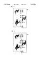
- FIG. 1is a block diagram showing the steps in making plated through-hole vias in a substrate
- FIGS. 2-4illustrate a typical substrate during successive steps in the process of FIG. 1.
- the first step in making viasis to provide an insulating substrate having at least a pair of major surfaces through which the via holes are to be formed. If the vias are to be formed in a ceramic, the initial substrate can be one or more layers of unsintered, green tape of the ceramic material.
- the next step shown in block Bis to form via holes in the substrate. This can be accomplished in a conventional manner using a punch press.
- FIG. 2illustrates a portion of a green tape substrate 20 having a plurality of punched via holes 21. Although the via holes shown in FIG. 2 are square, they can be rectangular, circular or any other shape.
- the third step(block C of FIG. 1) is to apply a thin, continuous coating of conductive material within the via holes.
- This coatingreferred to as a borecoat, is too thin to provide the desired final via conductivity, but it is useful in the subsequent plating process.
- a preferred way of providing the borecoatis to print a conductive ink through a metal mask using vacuum assist to coat the vertical sidewall surface of each conductive via.
- FIG. 3shows the substrate 20 after the vias 21 have received their borecoat 22.
- the next step, shown in block D,is to form in the substrate, apertures which intersect the borecoated vias.
- the aperturesare preferably rectangular and are punched in each tape layer such that aperture edges intersect a plurality via holes to form crenelated edges including a plurality of conductive edge vias. This is illustrated in FIG. 4 wherein apertures 40 intersect via holes 21.
- the aperturescan be circular or rectangular.
- surface metallization patternscan be applied.
- conductive pastecan be screen printed on one or more major surfaces of the tape.
- the fifth step(block E of FIG. 1) is to plate the borecoated vias with conductive metal.
- the substrateis a ceramic tape construction, as preliminary steps, the tape layers should be laminated together and sintered to produce a substrate with co-fired metallized regions. Metal, such as copper, is then plated onto the metallized regions to increase their thickness in a uniform manner. While the preferred embodiment is making conductive vias in ceramic substrates, the same method can be used with epoxy-glass printed circuit boards by substituting drilling for hole and aperture punching. The technique for drilling in printed circuit boards is well known and is described in Printed Circuit Handbook pp. 2.7-2.11, C. F. Coombs, Jr., ed (McGraw Hill, 1988) which is incorporated herein by reference.
- a metallized substratewas fabricated using the processes illustrated in FIGS. 1-4. Ferrite green tapes, 0.030 inch thick, were obtained from Steward Inc. (Chattanooga, Tenn.). Via hole patterns similar to those in FIG. 2 were obtained by punching to produce 40 ⁇ 40 mil square via holes on 60 mil centers in a 4 hole square pattern. A silver-palladium ink was printed through a metal mask using vacuum assist to coat the vertical side wall surface of each via hole to form borecoated vias (FIG. 3). Apertures were then punched in each tape layer such that the apertures edges intersected the via holes, as illustrated in FIG. 4, to form crenelated edges including a plurality of conductive edge vias. The apertures eliminated about 11% of each via perimeter. Silver-palladium paste was then used to screen print surface metallization patterns on the top side of the upper most tape layer and the bottom side of the lower most tape layer.
- Copperwas then deposited electrolytically using a CUPRACID copper plating bath with the CT basic leveller commercially available from Atotech (State College, Pa.).
- the plating bathwas held at 25° C. with a brightener concentration of 3 ml/L and a leveller concentration of 15 ml/L.
- the agitationwas provided by air sparging and periodic flow reversal using a modified horizontal rod agitator (Kocour Model A83) with a speed of 2.3 cm/sec and a forward and reverse cycle of two seconds.
- the plating ramwas approximately 1.67 mil/hour.
- the total copper thickness depositedwas about 4 mils.
- the samplewas cross sectioned to determine the copper thicknesses at the top and bottom surfaces, and inside the via.
- the copper thickness inside the viavaries between 85% and 110% of the average copper thickness on the substrate surface.
- a second similar samplewas made with slightly smaller via holes but no intersecting apertures prior to plating.
- the via holeswere 30 ⁇ 30 mils after sintering.
- the copper thickness inside the viavaries between 55% and 90% of the average copper thickness on the substrate.
- the improvement on the uniformity of the via thickness profilewould increase the thermal and electrical conductance.
- the effect of the improved copper thickness distribution inside the viais to increase the thermal conductance by about 75%.
Landscapes
- Engineering & Computer Science (AREA)
- Power Engineering (AREA)
- Microelectronics & Electronic Packaging (AREA)
- Manufacturing & Machinery (AREA)
- Ceramic Engineering (AREA)
- Physics & Mathematics (AREA)
- Condensed Matter Physics & Semiconductors (AREA)
- General Physics & Mathematics (AREA)
- Computer Hardware Design (AREA)
- Printing Elements For Providing Electric Connections Between Printed Circuits (AREA)
Abstract
Description
This is a continuation-in-part of U.S. patent application, Ser. No. 268,465, entitled "Devices Using Metallized Magnetic Substrates" and filed Jun. 30, 1994 by D. A. Fleming et al.
This invention relates to methods for fabricating plated through-hole vias between major surfaces of substrates such as circuit boards. The method provides highly conductive vias of enhanced plating uniformity.
Conductive vias are an important feature of circuit boards. There are two types of vias--filled vias and plated through-hole vias. Filled vias are typically used in co-fired, multilayer ceramic substrates. Plated vias are generally used in single or multilayer epoxy-glass circuit boards, although they can be used with ceramic substrates. Filled vias are solid columns extending between the two surfaces. Plated vias are hollow. This invention relates to plated vias.
Plated vias are used for either electrical or thermal conduction. Plated vias for electrical conduction provide electrical connection between conductors on one side of the board to those on the other, and to inner layer conductors in the case of multilayer boards. Plated vias for thermal conduction transfer heat generated from components on one side of the circuit board to the other for more efficient heat dissipation.
Current processing steps for fabricating plated vias are: (1) forming the via, (2) making the via inner wall surface conductive, and (3) electroplating copper on the circuit board, including vias. Because the via dimension is substantially smaller than that of the circuit board, the copper plating within the via is difficult to control and the thickness distribution tends to be non-uniform along the via. The non-uniformity of copper thickness distribution within the vias directly deteriorates the performance of both electrical and thermal vias. Accordingly, there is a need for an improved process for making vias of enhanced conductivity and uniformity.
The present inventors have discovered that the thickness uniformity of a plated metal layer inside a via hole can be enhanced by intersecting a conductive via with an insulating aperture before plating. The new via configuration improves the mass transfer of the plating. It is believed that the apertures lower the local solution ohmic resistance near the via holes. The method can be applied to the manufacture of a wide variety of circuit boards.
The advantages, nature and various additional features of the invention will appear more fully upon consideration of the illustrative embodiments now to be described in detail in connection with the accompanying drawings. In the drawings:
FIG. 1 is a block diagram showing the steps in making plated through-hole vias in a substrate;
FIGS. 2-4 illustrate a typical substrate during successive steps in the process of FIG. 1.
It is to be understood that these drawings are for purposes of illustrating the concepts of the invention and, except for graphical illustrations, are not to scale.
Referring to the drawings, as shown in FIG. 1, block A, the first step in making vias is to provide an insulating substrate having at least a pair of major surfaces through which the via holes are to be formed. If the vias are to be formed in a ceramic, the initial substrate can be one or more layers of unsintered, green tape of the ceramic material.
The next step shown in block B is to form via holes in the substrate. This can be accomplished in a conventional manner using a punch press. FIG. 2 illustrates a portion of agreen tape substrate 20 having a plurality of punched viaholes 21. Although the via holes shown in FIG. 2 are square, they can be rectangular, circular or any other shape.
The third step (block C of FIG. 1) is to apply a thin, continuous coating of conductive material within the via holes. This coating, referred to as a borecoat, is too thin to provide the desired final via conductivity, but it is useful in the subsequent plating process. A preferred way of providing the borecoat is to print a conductive ink through a metal mask using vacuum assist to coat the vertical sidewall surface of each conductive via. FIG. 3 shows thesubstrate 20 after thevias 21 have received theirborecoat 22.
The next step, shown in block D, is to form in the substrate, apertures which intersect the borecoated vias. For rectangular vias, the apertures are preferably rectangular and are punched in each tape layer such that aperture edges intersect a plurality via holes to form crenelated edges including a plurality of conductive edge vias. This is illustrated in FIG. 4 whereinapertures 40 intersect viaholes 21. For round via holes, the apertures can be circular or rectangular.
Advantageously at this point, surface metallization patterns can be applied. For example, conductive paste can be screen printed on one or more major surfaces of the tape.
The fifth step (block E of FIG. 1) is to plate the borecoated vias with conductive metal. If the substrate is a ceramic tape construction, as preliminary steps, the tape layers should be laminated together and sintered to produce a substrate with co-fired metallized regions. Metal, such as copper, is then plated onto the metallized regions to increase their thickness in a uniform manner. While the preferred embodiment is making conductive vias in ceramic substrates, the same method can be used with epoxy-glass printed circuit boards by substituting drilling for hole and aperture punching. The technique for drilling in printed circuit boards is well known and is described in Printed Circuit Handbook pp. 2.7-2.11, C. F. Coombs, Jr., ed (McGraw Hill, 1988) which is incorporated herein by reference.
The invention and its advantages can be more clearly understood by consideration of the following specific example.
A metallized substrate was fabricated using the processes illustrated in FIGS. 1-4. Ferrite green tapes, 0.030 inch thick, were obtained from Steward Inc. (Chattanooga, Tenn.). Via hole patterns similar to those in FIG. 2 were obtained by punching to produce 40×40 mil square via holes on 60 mil centers in a 4 hole square pattern. A silver-palladium ink was printed through a metal mask using vacuum assist to coat the vertical side wall surface of each via hole to form borecoated vias (FIG. 3). Apertures were then punched in each tape layer such that the apertures edges intersected the via holes, as illustrated in FIG. 4, to form crenelated edges including a plurality of conductive edge vias. The apertures eliminated about 11% of each via perimeter. Silver-palladium paste was then used to screen print surface metallization patterns on the top side of the upper most tape layer and the bottom side of the lower most tape layer.
Four tape layers were then laminated together and sintered at 1145° C. for 10 hours to produce a co-fired metallized ferrite substrate. The sintered thickness was 100 mils. The final pattern after sintering shrinkage comprised 32×32 mil via holes and 32 mil apertures.
Copper was then deposited electrolytically using a CUPRACID copper plating bath with the CT basic leveller commercially available from Atotech (State College, Pa.). The plating bath was held at 25° C. with a brightener concentration of 3 ml/L and a leveller concentration of 15 ml/L. The agitation was provided by air sparging and periodic flow reversal using a modified horizontal rod agitator (Kocour Model A83) with a speed of 2.3 cm/sec and a forward and reverse cycle of two seconds. The plating ram was approximately 1.67 mil/hour. The total copper thickness deposited was about 4 mils.
The sample was cross sectioned to determine the copper thicknesses at the top and bottom surfaces, and inside the via. The copper thickness inside the via varies between 85% and 110% of the average copper thickness on the substrate surface.
To provide a basis for comparison, a second similar sample was made with slightly smaller via holes but no intersecting apertures prior to plating. The via holes were 30×30 mils after sintering. The copper thickness inside the via varies between 55% and 90% of the average copper thickness on the substrate. Thus the presence of the aperture resulted in significant improvement of copper thickness distribution inside the via. The improvement on the uniformity of the via thickness profile would increase the thermal and electrical conductance. The effect of the improved copper thickness distribution inside the via is to increase the thermal conductance by about 75%.
It is to be understood that the above-described embodiments are illustrative of only a few of the many possible specific embodiments which can represent applications of the principles of the invention. Numerous and varied other arrangements can be devised by those skilled in the art without departing from the spirit and scope of the invention.
Claims (6)
1. A method for making conductive vias in an insulating substrate comprising the steps of:
providing an insulating substrate having a pair of major surfaces;
forming a plurality of via through-holes in said substrate between said major surfaces;
applying a first coating of conductive material to said substrate within said via holes;
forming one or more apertures in said substrate intersecting said conductively coated via holes so that the peripheries of the resulting composite apertures include both conductively coated via portions and insulating portions; and
plating said conductively coated via portions with a second layer of conductor.
2. The method of claim 1 wherein said substrate is sintered ceramic and said via holes and said apertures are made by punching the ceramic prior to sintering.
3. The method of claim 1 wherein said substrate is printed circuit board and said via holes and apertures are made by drilling.
4. The method of claim 1 wherein said via holes are rectangular.
5. The method of claim 1 wherein said via holes are rectangular; said apertures are rectangular; and at least one aperture edge intersects a plurality of vias to form a crenelated edge including a plurality of conductive via edges.
6. The method of claim 1 wherein said second layer of conductor is copper.
Priority Applications (4)
| Application Number | Priority Date | Filing Date | Title |
|---|---|---|---|
| US08/430,963US5619791A (en) | 1994-06-30 | 1995-04-28 | Method for fabricating highly conductive vias |
| DE69600404TDE69600404T2 (en) | 1995-04-28 | 1996-04-17 | Process for the production of highly conductive contact holes |
| EP96302699AEP0740496B1 (en) | 1995-04-28 | 1996-04-17 | Method for fabricating highly conductive vias |
| JP8103009AJPH08307052A (en) | 1995-04-28 | 1996-04-25 | Method for manufacturing highly conductive vias |
Applications Claiming Priority (2)
| Application Number | Priority Date | Filing Date | Title |
|---|---|---|---|
| US26846594A | 1994-06-30 | 1994-06-30 | |
| US08/430,963US5619791A (en) | 1994-06-30 | 1995-04-28 | Method for fabricating highly conductive vias |
Related Parent Applications (1)
| Application Number | Title | Priority Date | Filing Date |
|---|---|---|---|
| US26846594AContinuation-In-Part | 1994-06-30 | 1994-06-30 |
Publications (1)
| Publication Number | Publication Date |
|---|---|
| US5619791Atrue US5619791A (en) | 1997-04-15 |
Family
ID=23709852
Family Applications (1)
| Application Number | Title | Priority Date | Filing Date |
|---|---|---|---|
| US08/430,963Expired - Fee RelatedUS5619791A (en) | 1994-06-30 | 1995-04-28 | Method for fabricating highly conductive vias |
Country Status (4)
| Country | Link |
|---|---|
| US (1) | US5619791A (en) |
| EP (1) | EP0740496B1 (en) |
| JP (1) | JPH08307052A (en) |
| DE (1) | DE69600404T2 (en) |
Cited By (68)
| Publication number | Priority date | Publication date | Assignee | Title |
|---|---|---|---|---|
| US6007758A (en)* | 1998-02-10 | 1999-12-28 | Lucent Technologies Inc. | Process for forming device comprising metallized magnetic substrates |
| US6016005A (en)* | 1998-02-09 | 2000-01-18 | Cellarosi; Mario J. | Multilayer, high density micro circuit module and method of manufacturing same |
| US6148500A (en)* | 1995-07-24 | 2000-11-21 | Autosplice Systems Inc. | Electronic inductive device and method for manufacturing |
| US6316830B1 (en) | 1998-12-17 | 2001-11-13 | Charles Wen Chyang Lin | Bumpless flip chip assembly with strips and via-fill |
| US6350632B1 (en) | 2000-09-20 | 2002-02-26 | Charles W. C. Lin | Semiconductor chip assembly with ball bond connection joint |
| US6350386B1 (en) | 2000-09-20 | 2002-02-26 | Charles W. C. Lin | Method of making a support circuit with a tapered through-hole for a semiconductor chip assembly |
| US6350633B1 (en) | 2000-08-22 | 2002-02-26 | Charles W. C. Lin | Semiconductor chip assembly with simultaneously electroplated contact terminal and connection joint |
| US6402970B1 (en) | 2000-08-22 | 2002-06-11 | Charles W. C. Lin | Method of making a support circuit for a semiconductor chip assembly |
| US6403400B2 (en) | 1998-12-17 | 2002-06-11 | Charles Wen Chyang Lin | Bumpless flip chip assembly with strips-in-via and plating |
| US6403460B1 (en) | 2000-08-22 | 2002-06-11 | Charles W. C. Lin | Method of making a semiconductor chip assembly |
| US6406939B1 (en) | 1998-05-02 | 2002-06-18 | Charles W. C. Lin | Flip chip assembly with via interconnection |
| US6436734B1 (en) | 2000-08-22 | 2002-08-20 | Charles W. C. Lin | Method of making a support circuit for a semiconductor chip assembly |
| US6440835B1 (en) | 2000-10-13 | 2002-08-27 | Charles W. C. Lin | Method of connecting a conductive trace to a semiconductor chip |
| US6444489B1 (en) | 2000-12-15 | 2002-09-03 | Charles W. C. Lin | Semiconductor chip assembly with bumped molded substrate |
| US6448108B1 (en) | 2000-10-02 | 2002-09-10 | Charles W. C. Lin | Method of making a semiconductor chip assembly with a conductive trace subtractively formed before and after chip attachment |
| US6448644B1 (en) | 1998-05-02 | 2002-09-10 | Charles W. C. Lin | Flip chip assembly with via interconnection |
| US6492252B1 (en) | 2000-10-13 | 2002-12-10 | Bridge Semiconductor Corporation | Method of connecting a bumped conductive trace to a semiconductor chip |
| US6511865B1 (en) | 2000-09-20 | 2003-01-28 | Charles W. C. Lin | Method for forming a ball bond connection joint on a conductive trace and conductive pad in a semiconductor chip assembly |
| US6528891B2 (en) | 1998-12-17 | 2003-03-04 | Charles Wen Chyang Lin | Bumpless flip chip assembly with solder via |
| US6537851B1 (en) | 2000-10-13 | 2003-03-25 | Bridge Semiconductor Corporation | Method of connecting a bumped compliant conductive trace to a semiconductor chip |
| US6544813B1 (en) | 2000-10-02 | 2003-04-08 | Charles W. C. Lin | Method of making a semiconductor chip assembly with a conductive trace subtractively formed before and after chip attachment |
| US6548393B1 (en) | 2000-10-13 | 2003-04-15 | Charles W. C. Lin | Semiconductor chip assembly with hardened connection joint |
| US6551861B1 (en) | 2000-08-22 | 2003-04-22 | Charles W. C. Lin | Method of making a semiconductor chip assembly by joining the chip to a support circuit with an adhesive |
| US6562657B1 (en) | 2000-08-22 | 2003-05-13 | Charles W. C. Lin | Semiconductor chip assembly with simultaneously electrolessly plated contact terminal and connection joint |
| US6562709B1 (en) | 2000-08-22 | 2003-05-13 | Charles W. C. Lin | Semiconductor chip assembly with simultaneously electroplated contact terminal and connection joint |
| US6576539B1 (en) | 2000-10-13 | 2003-06-10 | Charles W.C. Lin | Semiconductor chip assembly with interlocked conductive trace |
| US6576493B1 (en) | 2000-10-13 | 2003-06-10 | Bridge Semiconductor Corporation | Method of connecting a conductive trace and an insulative base to a semiconductor chip using multiple etch steps |
| US6583040B1 (en) | 2000-10-13 | 2003-06-24 | Bridge Semiconductor Corporation | Method of making a pillar in a laminated structure for a semiconductor chip assembly |
| US6653170B1 (en) | 2001-02-06 | 2003-11-25 | Charles W. C. Lin | Semiconductor chip assembly with elongated wire ball bonded to chip and electrolessly plated to support circuit |
| US6660626B1 (en) | 2000-08-22 | 2003-12-09 | Charles W. C. Lin | Semiconductor chip assembly with simultaneously electrolessly plated contact terminal and connection joint |
| US6663442B1 (en) | 2000-01-27 | 2003-12-16 | Tyco Electronics Corporation | High speed interconnect using printed circuit board with plated bores |
| US6667229B1 (en) | 2000-10-13 | 2003-12-23 | Bridge Semiconductor Corporation | Method of connecting a bumped compliant conductive trace and an insulative base to a semiconductor chip |
| US6699780B1 (en) | 2000-10-13 | 2004-03-02 | Bridge Semiconductor Corporation | Method of connecting a conductive trace to a semiconductor chip using plasma undercut etching |
| US6740576B1 (en) | 2000-10-13 | 2004-05-25 | Bridge Semiconductor Corporation | Method of making a contact terminal with a plated metal peripheral sidewall portion for a semiconductor chip assembly |
| US6872591B1 (en) | 2000-10-13 | 2005-03-29 | Bridge Semiconductor Corporation | Method of making a semiconductor chip assembly with a conductive trace and a substrate |
| US6876072B1 (en) | 2000-10-13 | 2005-04-05 | Bridge Semiconductor Corporation | Semiconductor chip assembly with chip in substrate cavity |
| US6908788B1 (en) | 2000-10-13 | 2005-06-21 | Bridge Semiconductor Corporation | Method of connecting a conductive trace to a semiconductor chip using a metal base |
| US6949408B1 (en) | 2000-10-13 | 2005-09-27 | Bridge Semiconductor Corporation | Method of connecting a conductive trace and an insulative base to a semiconductor chip using multiple etch steps |
| US6984576B1 (en) | 2000-10-13 | 2006-01-10 | Bridge Semiconductor Corporation | Method of connecting an additively and subtractively formed conductive trace and an insulative base to a semiconductor chip |
| US20060012024A1 (en)* | 2000-10-13 | 2006-01-19 | Bridge Semiconductor Corporation | Semiconductor chip assembly with metal containment wall and solder terminal |
| US20060043598A1 (en)* | 2004-08-31 | 2006-03-02 | Kirby Kyle K | Methods of manufacture of a via structure comprising a plurality of conductive elements, semiconductor die, multichip module, and system including same |
| US7009297B1 (en) | 2000-10-13 | 2006-03-07 | Bridge Semiconductor Corporation | Semiconductor chip assembly with embedded metal particle |
| US7071089B1 (en) | 2000-10-13 | 2006-07-04 | Bridge Semiconductor Corporation | Method of making a semiconductor chip assembly with a carved bumped terminal |
| US7075186B1 (en) | 2000-10-13 | 2006-07-11 | Bridge Semiconductor Corporation | Semiconductor chip assembly with interlocked contact terminal |
| US7094676B1 (en) | 2000-10-13 | 2006-08-22 | Bridge Semiconductor Corporation | Semiconductor chip assembly with embedded metal pillar |
| US7112521B1 (en) | 2000-10-13 | 2006-09-26 | Bridge Semiconductor Corporation | Method of making a semiconductor chip assembly with a bumped metal pillar |
| US7129113B1 (en) | 2000-10-13 | 2006-10-31 | Bridge Semiconductor Corporation | Method of making a three-dimensional stacked semiconductor package with a metal pillar in an encapsulant aperture |
| US7132741B1 (en) | 2000-10-13 | 2006-11-07 | Bridge Semiconductor Corporation | Semiconductor chip assembly with carved bumped terminal |
| US7190080B1 (en) | 2000-10-13 | 2007-03-13 | Bridge Semiconductor Corporation | Semiconductor chip assembly with embedded metal pillar |
| US20070080760A1 (en)* | 2005-10-11 | 2007-04-12 | Alford James L | Printed wiring board assembly with self-compensating ground via |
| US20070194431A1 (en)* | 2006-02-20 | 2007-08-23 | Corisis David J | Conductive vias having two or more conductive elements for providing electrical communication between traces in different planes in a substrate, semiconductor device assemblies including such vias, and accompanying methods |
| US7262082B1 (en) | 2000-10-13 | 2007-08-28 | Bridge Semiconductor Corporation | Method of making a three-dimensional stacked semiconductor package with a metal pillar and a conductive interconnect in an encapsulant aperture |
| US7264991B1 (en) | 2000-10-13 | 2007-09-04 | Bridge Semiconductor Corporation | Method of connecting a conductive trace to a semiconductor chip using conductive adhesive |
| US7268421B1 (en) | 2004-11-10 | 2007-09-11 | Bridge Semiconductor Corporation | Semiconductor chip assembly with welded metal pillar that includes enlarged ball bond |
| US7319265B1 (en) | 2000-10-13 | 2008-01-15 | Bridge Semiconductor Corporation | Semiconductor chip assembly with precision-formed metal pillar |
| US7396703B1 (en) | 2003-11-20 | 2008-07-08 | Bridge Semiconductor Corporation | Method of making a semiconductor chip assembly with a bumped terminal and a filler |
| US20080266824A1 (en)* | 2007-04-29 | 2008-10-30 | Premier Image Technology(China) Ltd. | Pad and circuit board, electronic device using same |
| US7446419B1 (en) | 2004-11-10 | 2008-11-04 | Bridge Semiconductor Corporation | Semiconductor chip assembly with welded metal pillar of stacked metal balls |
| US7494843B1 (en) | 2006-12-26 | 2009-02-24 | Bridge Semiconductor Corporation | Method of making a semiconductor chip assembly with thermal conductor and encapsulant grinding |
| US7538415B1 (en) | 2003-11-20 | 2009-05-26 | Bridge Semiconductor Corporation | Semiconductor chip assembly with bumped terminal, filler and insulative base |
| US7750483B1 (en) | 2004-11-10 | 2010-07-06 | Bridge Semiconductor Corporation | Semiconductor chip assembly with welded metal pillar and enlarged plated contact terminal |
| US7811863B1 (en) | 2006-10-26 | 2010-10-12 | Bridge Semiconductor Corporation | Method of making a semiconductor chip assembly with metal pillar and encapsulant grinding and heat sink attachment |
| US7993983B1 (en) | 2003-11-17 | 2011-08-09 | Bridge Semiconductor Corporation | Method of making a semiconductor chip assembly with chip and encapsulant grinding |
| US9887449B2 (en)* | 2014-08-29 | 2018-02-06 | Nxp Usa, Inc. | Radio frequency coupling structure and a method of manufacturing thereof |
| US9917372B2 (en) | 2014-06-13 | 2018-03-13 | Nxp Usa, Inc. | Integrated circuit package with radio frequency coupling arrangement |
| US10103447B2 (en) | 2014-06-13 | 2018-10-16 | Nxp Usa, Inc. | Integrated circuit package with radio frequency coupling structure |
| US10225925B2 (en)* | 2014-08-29 | 2019-03-05 | Nxp Usa, Inc. | Radio frequency coupling and transition structure |
| US10813214B2 (en)* | 2011-11-15 | 2020-10-20 | Invensas Corporation | Cavities containing multi-wiring structures and devices |
Citations (18)
| Publication number | Priority date | Publication date | Assignee | Title |
|---|---|---|---|---|
| US3349480A (en)* | 1962-11-09 | 1967-10-31 | Ibm | Method of forming through hole conductor lines |
| JPS5439322A (en)* | 1977-06-22 | 1979-03-26 | Johnson & Nephew Ambergate Inc | Method and apparatus for metal filaments |
| JPS56120058A (en)* | 1980-02-27 | 1981-09-21 | Hitachi Ltd | Electron gun for picture tube |
| JPS56152447A (en)* | 1980-04-28 | 1981-11-26 | Sumitomo Chem Co Ltd | N-dimethylbenzyl-tert-butylacetamide derivative, its preparation, and herbicide comprising it as active ingredient |
| JPS59212335A (en)* | 1984-04-26 | 1984-12-01 | Fuji Photo Film Co Ltd | Method of separating flexible sheet |
| US4522671A (en)* | 1981-11-17 | 1985-06-11 | Robert Bosch Gmbh | Method of applying an electrical conductor pattern on an apertured substrate |
| US4543715A (en)* | 1983-02-28 | 1985-10-01 | Allied Corporation | Method of forming vertical traces on printed circuit board |
| JPS62254879A (en)* | 1986-04-28 | 1987-11-06 | Toshiba Corp | Coloring method |
| US4775465A (en)* | 1984-12-24 | 1988-10-04 | Burrows Bruce D | Reverse osmosis assembly operating valve |
| JPS63297083A (en)* | 1987-05-29 | 1988-12-05 | Brother Ind Ltd | electronic typewriter |
| JPH01297487A (en)* | 1988-05-26 | 1989-11-30 | Mitsubishi Monsanto Chem Co | Composition for abrasion |
| JPH02232986A (en)* | 1989-03-07 | 1990-09-14 | Sony Corp | Board and manufacture thereof |
| US5029043A (en)* | 1989-03-23 | 1991-07-02 | Mitsubishi Mining And Cement Co., Ltd. | LC circuit incorporated ceramic substrate |
| EP0467698A2 (en)* | 1990-07-20 | 1992-01-22 | Nortel Networks Corporation | Printed circuit board having holes with multiple conductors |
| GB2252208A (en)* | 1991-01-24 | 1992-07-29 | Burr Brown Corp | Hybrid integrated circuit planar transformer |
| US5136120A (en)* | 1989-12-20 | 1992-08-04 | At&T Bell Laboratories | Technique for reducing electromagnetic interference |
| US5161098A (en)* | 1991-09-09 | 1992-11-03 | Power Integrations, Inc. | High frequency switched mode converter |
| US5239744A (en)* | 1992-01-09 | 1993-08-31 | At&T Bell Laboratories | Method for making multilayer magnetic components |
- 1995
- 1995-04-28USUS08/430,963patent/US5619791A/ennot_activeExpired - Fee Related
- 1996
- 1996-04-17EPEP96302699Apatent/EP0740496B1/ennot_activeExpired - Lifetime
- 1996-04-17DEDE69600404Tpatent/DE69600404T2/ennot_activeExpired - Fee Related
- 1996-04-25JPJP8103009Apatent/JPH08307052A/enactivePending
Patent Citations (18)
| Publication number | Priority date | Publication date | Assignee | Title |
|---|---|---|---|---|
| US3349480A (en)* | 1962-11-09 | 1967-10-31 | Ibm | Method of forming through hole conductor lines |
| JPS5439322A (en)* | 1977-06-22 | 1979-03-26 | Johnson & Nephew Ambergate Inc | Method and apparatus for metal filaments |
| JPS56120058A (en)* | 1980-02-27 | 1981-09-21 | Hitachi Ltd | Electron gun for picture tube |
| JPS56152447A (en)* | 1980-04-28 | 1981-11-26 | Sumitomo Chem Co Ltd | N-dimethylbenzyl-tert-butylacetamide derivative, its preparation, and herbicide comprising it as active ingredient |
| US4522671A (en)* | 1981-11-17 | 1985-06-11 | Robert Bosch Gmbh | Method of applying an electrical conductor pattern on an apertured substrate |
| US4543715A (en)* | 1983-02-28 | 1985-10-01 | Allied Corporation | Method of forming vertical traces on printed circuit board |
| JPS59212335A (en)* | 1984-04-26 | 1984-12-01 | Fuji Photo Film Co Ltd | Method of separating flexible sheet |
| US4775465A (en)* | 1984-12-24 | 1988-10-04 | Burrows Bruce D | Reverse osmosis assembly operating valve |
| JPS62254879A (en)* | 1986-04-28 | 1987-11-06 | Toshiba Corp | Coloring method |
| JPS63297083A (en)* | 1987-05-29 | 1988-12-05 | Brother Ind Ltd | electronic typewriter |
| JPH01297487A (en)* | 1988-05-26 | 1989-11-30 | Mitsubishi Monsanto Chem Co | Composition for abrasion |
| JPH02232986A (en)* | 1989-03-07 | 1990-09-14 | Sony Corp | Board and manufacture thereof |
| US5029043A (en)* | 1989-03-23 | 1991-07-02 | Mitsubishi Mining And Cement Co., Ltd. | LC circuit incorporated ceramic substrate |
| US5136120A (en)* | 1989-12-20 | 1992-08-04 | At&T Bell Laboratories | Technique for reducing electromagnetic interference |
| EP0467698A2 (en)* | 1990-07-20 | 1992-01-22 | Nortel Networks Corporation | Printed circuit board having holes with multiple conductors |
| GB2252208A (en)* | 1991-01-24 | 1992-07-29 | Burr Brown Corp | Hybrid integrated circuit planar transformer |
| US5161098A (en)* | 1991-09-09 | 1992-11-03 | Power Integrations, Inc. | High frequency switched mode converter |
| US5239744A (en)* | 1992-01-09 | 1993-08-31 | At&T Bell Laboratories | Method for making multilayer magnetic components |
Non-Patent Citations (10)
| Title |
|---|
| "An Inductor/Capacitor Hybrid Made of Ferrite Only", Sakak, Autor; pp. 3009-3011, IEEE Transactions on Magnetics, vol. 28, No. 5, Sep. 1992. |
| "Design of High-Frequency Hybrid Power Transformer", Grtadzki and Lee, Authors; pp. 319-326, IEEE, 1988/CH2504-9/88/0000-0319. |
| "Electronic Materials Handbook", vol. 1-Packaging, prepared/ASM International, Handbook Committee, of ASM International, Materials Park, OH 44073, pp. 187-189. |
| Abstract "Development of Miniaturized DC-DC Converter with Multilayer Ceramic Transformer", Takaya, Mochizuki, Nakano, Kobuke, Authors; pp. 269-574, ISHM"92 Proceedings. |
| Abstract Development of Miniaturized DC DC Converter with Multilayer Ceramic Transformer , Takaya, Mochizuki, Nakano, Kobuke, Authors; pp. 269 574, ISHM 92 Proceedings.* |
| An Inductor/Capacitor Hybrid Made of Ferrite Only , Sakak, Autor; pp. 3009 3011, IEEE Transactions on Magnetics, vol. 28, No. 5, Sep. 1992.* |
| Design of High Frequency Hybrid Power Transformer , Grtadzki and Lee, Authors; pp. 319 326, IEEE, 1988/CH2504 9/88/0000 0319.* |
| Electronic Materials Handbook , vol. 1 Packaging, prepared/ASM International, Handbook Committee, of ASM International, Materials Park, OH 44073, pp. 187 189.* |
| Patent Abstract of Japan, vol. 14, No. 546 (E 1008), Dec. 4, 1990 & JP A 02 232986 (Sony Corp.), 14 Sep. 1990.* |
| Patent Abstract of Japan, vol. 14, No. 546 (E-1008), Dec. 4, 1990 & JP-A-02 232986 (Sony Corp.), 14 Sep. 1990. |
Cited By (108)
| Publication number | Priority date | Publication date | Assignee | Title |
|---|---|---|---|---|
| US6148500A (en)* | 1995-07-24 | 2000-11-21 | Autosplice Systems Inc. | Electronic inductive device and method for manufacturing |
| US6016005A (en)* | 1998-02-09 | 2000-01-18 | Cellarosi; Mario J. | Multilayer, high density micro circuit module and method of manufacturing same |
| US6242286B1 (en) | 1998-02-09 | 2001-06-05 | Mario J. Cellarosi | Multilayer high density micro circuit module and method of manufacturing same |
| US6153078A (en)* | 1998-02-10 | 2000-11-28 | Lucent Technologies Inc. | Process for forming device comprising metallized magnetic substrates |
| US6007758A (en)* | 1998-02-10 | 1999-12-28 | Lucent Technologies Inc. | Process for forming device comprising metallized magnetic substrates |
| US6406939B1 (en) | 1998-05-02 | 2002-06-18 | Charles W. C. Lin | Flip chip assembly with via interconnection |
| US6448644B1 (en) | 1998-05-02 | 2002-09-10 | Charles W. C. Lin | Flip chip assembly with via interconnection |
| US6403400B2 (en) | 1998-12-17 | 2002-06-11 | Charles Wen Chyang Lin | Bumpless flip chip assembly with strips-in-via and plating |
| US6437452B2 (en) | 1998-12-17 | 2002-08-20 | Charles Wen Chyang Lin | Bumpless flip chip assembly with strips-in-via and plating |
| US6528891B2 (en) | 1998-12-17 | 2003-03-04 | Charles Wen Chyang Lin | Bumpless flip chip assembly with solder via |
| US6475833B2 (en) | 1998-12-17 | 2002-11-05 | Charles Wen Chyang Lin | Bumpless flip chip assembly with strips and via-fill |
| US6316830B1 (en) | 1998-12-17 | 2001-11-13 | Charles Wen Chyang Lin | Bumpless flip chip assembly with strips and via-fill |
| US6663442B1 (en) | 2000-01-27 | 2003-12-16 | Tyco Electronics Corporation | High speed interconnect using printed circuit board with plated bores |
| DE10195164B4 (en) | 2000-01-27 | 2021-10-14 | Te Connectivity Corporation | High speed connection |
| US6403460B1 (en) | 2000-08-22 | 2002-06-11 | Charles W. C. Lin | Method of making a semiconductor chip assembly |
| US6436734B1 (en) | 2000-08-22 | 2002-08-20 | Charles W. C. Lin | Method of making a support circuit for a semiconductor chip assembly |
| US6562657B1 (en) | 2000-08-22 | 2003-05-13 | Charles W. C. Lin | Semiconductor chip assembly with simultaneously electrolessly plated contact terminal and connection joint |
| US6551861B1 (en) | 2000-08-22 | 2003-04-22 | Charles W. C. Lin | Method of making a semiconductor chip assembly by joining the chip to a support circuit with an adhesive |
| US6562709B1 (en) | 2000-08-22 | 2003-05-13 | Charles W. C. Lin | Semiconductor chip assembly with simultaneously electroplated contact terminal and connection joint |
| US6350633B1 (en) | 2000-08-22 | 2002-02-26 | Charles W. C. Lin | Semiconductor chip assembly with simultaneously electroplated contact terminal and connection joint |
| US6402970B1 (en) | 2000-08-22 | 2002-06-11 | Charles W. C. Lin | Method of making a support circuit for a semiconductor chip assembly |
| US6660626B1 (en) | 2000-08-22 | 2003-12-09 | Charles W. C. Lin | Semiconductor chip assembly with simultaneously electrolessly plated contact terminal and connection joint |
| US6350386B1 (en) | 2000-09-20 | 2002-02-26 | Charles W. C. Lin | Method of making a support circuit with a tapered through-hole for a semiconductor chip assembly |
| US6511865B1 (en) | 2000-09-20 | 2003-01-28 | Charles W. C. Lin | Method for forming a ball bond connection joint on a conductive trace and conductive pad in a semiconductor chip assembly |
| US6627824B1 (en) | 2000-09-20 | 2003-09-30 | Charles W. C. Lin | Support circuit with a tapered through-hole for a semiconductor chip assembly |
| US6350632B1 (en) | 2000-09-20 | 2002-02-26 | Charles W. C. Lin | Semiconductor chip assembly with ball bond connection joint |
| US6544813B1 (en) | 2000-10-02 | 2003-04-08 | Charles W. C. Lin | Method of making a semiconductor chip assembly with a conductive trace subtractively formed before and after chip attachment |
| US6448108B1 (en) | 2000-10-02 | 2002-09-10 | Charles W. C. Lin | Method of making a semiconductor chip assembly with a conductive trace subtractively formed before and after chip attachment |
| US7015128B1 (en) | 2000-10-13 | 2006-03-21 | Bridge Semiconductor Corporation | Method of making a semiconductor chip assembly with an embedded metal particle |
| US7190080B1 (en) | 2000-10-13 | 2007-03-13 | Bridge Semiconductor Corporation | Semiconductor chip assembly with embedded metal pillar |
| US6576493B1 (en) | 2000-10-13 | 2003-06-10 | Bridge Semiconductor Corporation | Method of connecting a conductive trace and an insulative base to a semiconductor chip using multiple etch steps |
| US6583040B1 (en) | 2000-10-13 | 2003-06-24 | Bridge Semiconductor Corporation | Method of making a pillar in a laminated structure for a semiconductor chip assembly |
| US6608374B1 (en) | 2000-10-13 | 2003-08-19 | Bridge Semiconductor Corporation | Semiconductor chip assembly with bumped conductive trace |
| US6548393B1 (en) | 2000-10-13 | 2003-04-15 | Charles W. C. Lin | Semiconductor chip assembly with hardened connection joint |
| US6440835B1 (en) | 2000-10-13 | 2002-08-27 | Charles W. C. Lin | Method of connecting a conductive trace to a semiconductor chip |
| US6653742B1 (en) | 2000-10-13 | 2003-11-25 | Charles W. C. Lin | Semiconductor chip assembly with interlocked conductive trace |
| US6653217B1 (en) | 2000-10-13 | 2003-11-25 | Charles W. C. Lin | Method of connecting a conductive trace to a semiconductor chip |
| US6537851B1 (en) | 2000-10-13 | 2003-03-25 | Bridge Semiconductor Corporation | Method of connecting a bumped compliant conductive trace to a semiconductor chip |
| US6492252B1 (en) | 2000-10-13 | 2002-12-10 | Bridge Semiconductor Corporation | Method of connecting a bumped conductive trace to a semiconductor chip |
| US6667229B1 (en) | 2000-10-13 | 2003-12-23 | Bridge Semiconductor Corporation | Method of connecting a bumped compliant conductive trace and an insulative base to a semiconductor chip |
| US6673710B1 (en) | 2000-10-13 | 2004-01-06 | Bridge Semiconductor Corporation | Method of connecting a conductive trace and an insulative base to a semiconductor chip |
| US6699780B1 (en) | 2000-10-13 | 2004-03-02 | Bridge Semiconductor Corporation | Method of connecting a conductive trace to a semiconductor chip using plasma undercut etching |
| US6740576B1 (en) | 2000-10-13 | 2004-05-25 | Bridge Semiconductor Corporation | Method of making a contact terminal with a plated metal peripheral sidewall portion for a semiconductor chip assembly |
| US6800506B1 (en) | 2000-10-13 | 2004-10-05 | Bridge Semiconductor Corporation | Method of making a bumped terminal in a laminated structure for a semiconductor chip assembly |
| US6809414B1 (en) | 2000-10-13 | 2004-10-26 | Bridge Semiconductor Corporation | Semiconductor chip assembly with bumped conductive trace |
| US6872591B1 (en) | 2000-10-13 | 2005-03-29 | Bridge Semiconductor Corporation | Method of making a semiconductor chip assembly with a conductive trace and a substrate |
| US6876072B1 (en) | 2000-10-13 | 2005-04-05 | Bridge Semiconductor Corporation | Semiconductor chip assembly with chip in substrate cavity |
| US6908788B1 (en) | 2000-10-13 | 2005-06-21 | Bridge Semiconductor Corporation | Method of connecting a conductive trace to a semiconductor chip using a metal base |
| US6949408B1 (en) | 2000-10-13 | 2005-09-27 | Bridge Semiconductor Corporation | Method of connecting a conductive trace and an insulative base to a semiconductor chip using multiple etch steps |
| US6984576B1 (en) | 2000-10-13 | 2006-01-10 | Bridge Semiconductor Corporation | Method of connecting an additively and subtractively formed conductive trace and an insulative base to a semiconductor chip |
| US20060012024A1 (en)* | 2000-10-13 | 2006-01-19 | Bridge Semiconductor Corporation | Semiconductor chip assembly with metal containment wall and solder terminal |
| US20060014316A1 (en)* | 2000-10-13 | 2006-01-19 | Bridge Semiconductor Corporation | Method of making a semiconductor chip assemby with a metal containment wall and a solder terminal |
| US7419851B2 (en) | 2000-10-13 | 2008-09-02 | Bridge Semiconductor Corporation | Method of making a semiconductor chip assembly with a metal containment wall and a solder terminal |
| US7009297B1 (en) | 2000-10-13 | 2006-03-07 | Bridge Semiconductor Corporation | Semiconductor chip assembly with embedded metal particle |
| US7414319B2 (en) | 2000-10-13 | 2008-08-19 | Bridge Semiconductor Corporation | Semiconductor chip assembly with metal containment wall and solder terminal |
| US7319265B1 (en) | 2000-10-13 | 2008-01-15 | Bridge Semiconductor Corporation | Semiconductor chip assembly with precision-formed metal pillar |
| US7067911B1 (en) | 2000-10-13 | 2006-06-27 | Bridge Semiconductor Corporation | Three-dimensional stacked semiconductor package with metal pillar in encapsulant aperture |
| US7071573B1 (en) | 2000-10-13 | 2006-07-04 | Bridge Semiconductor Corporation | Semiconductor chip assembly with welded metal pillar |
| US7071089B1 (en) | 2000-10-13 | 2006-07-04 | Bridge Semiconductor Corporation | Method of making a semiconductor chip assembly with a carved bumped terminal |
| US7075186B1 (en) | 2000-10-13 | 2006-07-11 | Bridge Semiconductor Corporation | Semiconductor chip assembly with interlocked contact terminal |
| US7264991B1 (en) | 2000-10-13 | 2007-09-04 | Bridge Semiconductor Corporation | Method of connecting a conductive trace to a semiconductor chip using conductive adhesive |
| US7094676B1 (en) | 2000-10-13 | 2006-08-22 | Bridge Semiconductor Corporation | Semiconductor chip assembly with embedded metal pillar |
| US7112521B1 (en) | 2000-10-13 | 2006-09-26 | Bridge Semiconductor Corporation | Method of making a semiconductor chip assembly with a bumped metal pillar |
| US7262082B1 (en) | 2000-10-13 | 2007-08-28 | Bridge Semiconductor Corporation | Method of making a three-dimensional stacked semiconductor package with a metal pillar and a conductive interconnect in an encapsulant aperture |
| US7129575B1 (en) | 2000-10-13 | 2006-10-31 | Bridge Semiconductor Corporation | Semiconductor chip assembly with bumped metal pillar |
| US7129113B1 (en) | 2000-10-13 | 2006-10-31 | Bridge Semiconductor Corporation | Method of making a three-dimensional stacked semiconductor package with a metal pillar in an encapsulant aperture |
| US7132741B1 (en) | 2000-10-13 | 2006-11-07 | Bridge Semiconductor Corporation | Semiconductor chip assembly with carved bumped terminal |
| US6576539B1 (en) | 2000-10-13 | 2003-06-10 | Charles W.C. Lin | Semiconductor chip assembly with interlocked conductive trace |
| US7232707B1 (en) | 2000-10-13 | 2007-06-19 | Bridge Semiconductor Corporation | Method of making a semiconductor chip assembly with an interlocked contact terminal |
| US7232706B1 (en) | 2000-10-13 | 2007-06-19 | Bridge Semiconductor Corporation | Method of making a semiconductor chip assembly with a precision-formed metal pillar |
| US6444489B1 (en) | 2000-12-15 | 2002-09-03 | Charles W. C. Lin | Semiconductor chip assembly with bumped molded substrate |
| US6653170B1 (en) | 2001-02-06 | 2003-11-25 | Charles W. C. Lin | Semiconductor chip assembly with elongated wire ball bonded to chip and electrolessly plated to support circuit |
| US7993983B1 (en) | 2003-11-17 | 2011-08-09 | Bridge Semiconductor Corporation | Method of making a semiconductor chip assembly with chip and encapsulant grinding |
| US7459385B1 (en) | 2003-11-20 | 2008-12-02 | Bridge Semiconductor Corporation | Method of making a semiconductor chip assembly with a laterally aligned bumped terminal and filler |
| US7417314B1 (en) | 2003-11-20 | 2008-08-26 | Bridge Semiconductor Corporation | Semiconductor chip assembly with laterally aligned bumped terminal and filler |
| US7932165B1 (en) | 2003-11-20 | 2011-04-26 | Bridge Semiconductor Corporation | Method of making a semiconductor chip assembly with a laterally aligned filler and insulative base |
| US7833827B1 (en) | 2003-11-20 | 2010-11-16 | Bridge Semiconductor Corporation | Method of making a semiconductor chip assembly with a bumped terminal, a filler and an insulative base |
| US7538415B1 (en) | 2003-11-20 | 2009-05-26 | Bridge Semiconductor Corporation | Semiconductor chip assembly with bumped terminal, filler and insulative base |
| US7453140B1 (en) | 2003-11-20 | 2008-11-18 | Bridge Semiconductor Corporation | Semiconductor chip assembly with laterally aligned filler and insulative base |
| US7396703B1 (en) | 2003-11-20 | 2008-07-08 | Bridge Semiconductor Corporation | Method of making a semiconductor chip assembly with a bumped terminal and a filler |
| US7425759B1 (en) | 2003-11-20 | 2008-09-16 | Bridge Semiconductor Corporation | Semiconductor chip assembly with bumped terminal and filler |
| US7129567B2 (en) | 2004-08-31 | 2006-10-31 | Micron Technology, Inc. | Substrate, semiconductor die, multichip module, and system including a via structure comprising a plurality of conductive elements |
| US20060125109A1 (en)* | 2004-08-31 | 2006-06-15 | Kirby Kyle K | Methods of manufacture of a via structure comprising a plurality of conductive elements and methods of forming multichip modules including such via structures |
| US20060043598A1 (en)* | 2004-08-31 | 2006-03-02 | Kirby Kyle K | Methods of manufacture of a via structure comprising a plurality of conductive elements, semiconductor die, multichip module, and system including same |
| US10448509B2 (en) | 2004-08-31 | 2019-10-15 | Micron Technology, Inc. | Electronic device assemblies including conductive vias having two or more conductive elements |
| US9084360B2 (en) | 2004-08-31 | 2015-07-14 | Micron Technology, Inc. | Electronic device assemblies including conductive vias having two or more conductive elements |
| US7355267B2 (en) | 2004-08-31 | 2008-04-08 | Micron Technology, Inc. | Substrate, semiconductor die, multichip module, and system including a via structure comprising a plurality of conductive elements |
| US20060180941A1 (en)* | 2004-08-31 | 2006-08-17 | Kirby Kyle K | Substrate, semiconductor die, multichip module, and system including a via structure comprising a plurality of conductive elements |
| US7495316B2 (en) | 2004-08-31 | 2009-02-24 | Micron Technology, Inc. | Methods of forming conductive vias and methods of forming multichip modules including such conductive vias |
| US20080029851A1 (en)* | 2004-08-31 | 2008-02-07 | Micron Technology, Inc. | Methods of forming conductive vias and methods of forming multichip modules including such conductive vias |
| US7282784B2 (en) | 2004-08-31 | 2007-10-16 | Micron Technology, Inc. | Methods of manufacture of a via structure comprising a plurality of conductive elements and methods of forming multichip modules including such via structures |
| US7446419B1 (en) | 2004-11-10 | 2008-11-04 | Bridge Semiconductor Corporation | Semiconductor chip assembly with welded metal pillar of stacked metal balls |
| US7268421B1 (en) | 2004-11-10 | 2007-09-11 | Bridge Semiconductor Corporation | Semiconductor chip assembly with welded metal pillar that includes enlarged ball bond |
| US7750483B1 (en) | 2004-11-10 | 2010-07-06 | Bridge Semiconductor Corporation | Semiconductor chip assembly with welded metal pillar and enlarged plated contact terminal |
| US20070080760A1 (en)* | 2005-10-11 | 2007-04-12 | Alford James L | Printed wiring board assembly with self-compensating ground via |
| US7411474B2 (en) | 2005-10-11 | 2008-08-12 | Andrew Corporation | Printed wiring board assembly with self-compensating ground via and current diverting cutout |
| US7767913B2 (en) | 2006-02-20 | 2010-08-03 | Micron Technology, Inc. | Electronic devices including conductive vias having two or more conductive elements for providing electrical communication between traces in different planes in a substrate, and accompanying methods |
| US8426743B2 (en) | 2006-02-20 | 2013-04-23 | Micron Technology, Inc. | Electronic device assemblies including conductive vias having two or more conductive elements |
| US20100284140A1 (en)* | 2006-02-20 | 2010-11-11 | Micron Technology, Inc. | Electronic device assemblies including conductive vias having two or more conductive elements |
| US20070194431A1 (en)* | 2006-02-20 | 2007-08-23 | Corisis David J | Conductive vias having two or more conductive elements for providing electrical communication between traces in different planes in a substrate, semiconductor device assemblies including such vias, and accompanying methods |
| US7811863B1 (en) | 2006-10-26 | 2010-10-12 | Bridge Semiconductor Corporation | Method of making a semiconductor chip assembly with metal pillar and encapsulant grinding and heat sink attachment |
| US7494843B1 (en) | 2006-12-26 | 2009-02-24 | Bridge Semiconductor Corporation | Method of making a semiconductor chip assembly with thermal conductor and encapsulant grinding |
| US20080266824A1 (en)* | 2007-04-29 | 2008-10-30 | Premier Image Technology(China) Ltd. | Pad and circuit board, electronic device using same |
| US10813214B2 (en)* | 2011-11-15 | 2020-10-20 | Invensas Corporation | Cavities containing multi-wiring structures and devices |
| US9917372B2 (en) | 2014-06-13 | 2018-03-13 | Nxp Usa, Inc. | Integrated circuit package with radio frequency coupling arrangement |
| US10103447B2 (en) | 2014-06-13 | 2018-10-16 | Nxp Usa, Inc. | Integrated circuit package with radio frequency coupling structure |
| US9887449B2 (en)* | 2014-08-29 | 2018-02-06 | Nxp Usa, Inc. | Radio frequency coupling structure and a method of manufacturing thereof |
| US10225925B2 (en)* | 2014-08-29 | 2019-03-05 | Nxp Usa, Inc. | Radio frequency coupling and transition structure |
Also Published As
| Publication number | Publication date |
|---|---|
| EP0740496A1 (en) | 1996-10-30 |
| DE69600404D1 (en) | 1998-08-13 |
| EP0740496B1 (en) | 1998-07-08 |
| JPH08307052A (en) | 1996-11-22 |
| DE69600404T2 (en) | 1999-02-11 |
Similar Documents
| Publication | Publication Date | Title |
|---|---|---|
| US5619791A (en) | Method for fabricating highly conductive vias | |
| US7348677B2 (en) | Method of providing printed circuit board with conductive holes and board resulting therefrom | |
| US4713494A (en) | Multilayer ceramic circuit board | |
| KR830008634A (en) | Manufacturing method of thick film fine pattern conductor | |
| US3568312A (en) | Method of making printed circuit boards | |
| JPS63144554A (en) | Manufacture of thick-film hybrid integrated circuit substrate | |
| JPH04199696A (en) | Landless high density via-hole filling method | |
| JPH01194394A (en) | Manufacture of multilayer printed-wiring board | |
| JPH02301187A (en) | Manufacturing method for double-sided wiring board | |
| JP2018011013A (en) | Method of making printed circuit board by semi-additive method | |
| JPH06196858A (en) | Manufacture of printed-circuit board | |
| JPH03229488A (en) | Manufacture of printed wiring board | |
| JPH0296389A (en) | Double-side printed circuit board | |
| JPH01257397A (en) | Metal printed board | |
| JPH0749823Y2 (en) | Circuit board | |
| JPS592198B2 (en) | Tasou Insatsu High Senban no Seizouhouhou | |
| JP2002171066A (en) | Method for manufacturing multilayer wiring board | |
| CN113811103A (en) | Printed circuit board and manufacturing method thereof | |
| JPH02185096A (en) | Thick film multilayer circuit board | |
| JPS60185403A (en) | Circuit board | |
| JPH08222823A (en) | Through hole wiring board | |
| JPS61253893A (en) | Circuit pattern formation | |
| JPH03288494A (en) | Via formation method for multilayer ceramic substrate | |
| JPH04287395A (en) | Electrolytic plating method for multilayer printed circuit boards | |
| JPH01313996A (en) | Printed wiring board manufacturing method |
Legal Events
| Date | Code | Title | Description |
|---|---|---|---|
| AS | Assignment | Owner name:LUCENT TECHNOLOGIES INC., NEW JERSEY Free format text:ASSIGNMENT OF ASSIGNORS INTEREST;ASSIGNOR:AT&T CORP.;REEL/FRAME:008684/0001 Effective date:19960329 | |
| FEPP | Fee payment procedure | Free format text:PAYOR NUMBER ASSIGNED (ORIGINAL EVENT CODE: ASPN); ENTITY STATUS OF PATENT OWNER: LARGE ENTITY | |
| FPAY | Fee payment | Year of fee payment:4 | |
| REMI | Maintenance fee reminder mailed | ||
| LAPS | Lapse for failure to pay maintenance fees | ||
| STCH | Information on status: patent discontinuation | Free format text:PATENT EXPIRED DUE TO NONPAYMENT OF MAINTENANCE FEES UNDER 37 CFR 1.362 | |
| FP | Lapsed due to failure to pay maintenance fee | Effective date:20050415 |