US5619067A - Semiconductor device package side-by-side stacking and mounting system - Google Patents
Semiconductor device package side-by-side stacking and mounting systemDownload PDFInfo
- Publication number
- US5619067A US5619067AUS08/236,768US23676894AUS5619067AUS 5619067 AUS5619067 AUS 5619067AUS 23676894 AUS23676894 AUS 23676894AUS 5619067 AUS5619067 AUS 5619067A
- Authority
- US
- United States
- Prior art keywords
- case
- array
- circuit board
- contact
- packages
- Prior art date
- Legal status (The legal status is an assumption and is not a legal conclusion. Google has not performed a legal analysis and makes no representation as to the accuracy of the status listed.)
- Expired - Lifetime
Links
Images


Classifications
- H—ELECTRICITY
- H05—ELECTRIC TECHNIQUES NOT OTHERWISE PROVIDED FOR
- H05K—PRINTED CIRCUITS; CASINGS OR CONSTRUCTIONAL DETAILS OF ELECTRIC APPARATUS; MANUFACTURE OF ASSEMBLAGES OF ELECTRICAL COMPONENTS
- H05K3/00—Apparatus or processes for manufacturing printed circuits
- H05K3/30—Assembling printed circuits with electric components, e.g. with resistor
- H05K3/303—Surface mounted components, e.g. affixing before soldering, aligning means, spacing means
- H—ELECTRICITY
- H01—ELECTRIC ELEMENTS
- H01L—SEMICONDUCTOR DEVICES NOT COVERED BY CLASS H10
- H01L25/00—Assemblies consisting of a plurality of semiconductor or other solid state devices
- H01L25/03—Assemblies consisting of a plurality of semiconductor or other solid state devices all the devices being of a type provided for in a single subclass of subclasses H10B, H10D, H10F, H10H, H10K or H10N, e.g. assemblies of rectifier diodes
- H01L25/10—Assemblies consisting of a plurality of semiconductor or other solid state devices all the devices being of a type provided for in a single subclass of subclasses H10B, H10D, H10F, H10H, H10K or H10N, e.g. assemblies of rectifier diodes the devices having separate containers
- H01L25/105—Assemblies consisting of a plurality of semiconductor or other solid state devices all the devices being of a type provided for in a single subclass of subclasses H10B, H10D, H10F, H10H, H10K or H10N, e.g. assemblies of rectifier diodes the devices having separate containers the devices being integrated devices of class H10
- H—ELECTRICITY
- H01—ELECTRIC ELEMENTS
- H01L—SEMICONDUCTOR DEVICES NOT COVERED BY CLASS H10
- H01L2225/00—Details relating to assemblies covered by the group H01L25/00 but not provided for in its subgroups
- H01L2225/03—All the devices being of a type provided for in the same main group of the same subclass of class H10, e.g. assemblies of rectifier diodes
- H01L2225/10—All the devices being of a type provided for in the same main group of the same subclass of class H10, e.g. assemblies of rectifier diodes the devices having separate containers
- H01L2225/1005—All the devices being of a type provided for in the same main group of the same subclass of class H10, e.g. assemblies of rectifier diodes the devices having separate containers the devices being integrated devices of class H10
- H01L2225/1011—All the devices being of a type provided for in the same main group of the same subclass of class H10, e.g. assemblies of rectifier diodes the devices having separate containers the devices being integrated devices of class H10 the containers being in a stacked arrangement
- H01L2225/1017—All the devices being of a type provided for in the same main group of the same subclass of class H10, e.g. assemblies of rectifier diodes the devices having separate containers the devices being integrated devices of class H10 the containers being in a stacked arrangement the lowermost container comprising a device support
- H01L2225/1029—All the devices being of a type provided for in the same main group of the same subclass of class H10, e.g. assemblies of rectifier diodes the devices having separate containers the devices being integrated devices of class H10 the containers being in a stacked arrangement the lowermost container comprising a device support the support being a lead frame
- H—ELECTRICITY
- H01—ELECTRIC ELEMENTS
- H01L—SEMICONDUCTOR DEVICES NOT COVERED BY CLASS H10
- H01L2225/00—Details relating to assemblies covered by the group H01L25/00 but not provided for in its subgroups
- H01L2225/03—All the devices being of a type provided for in the same main group of the same subclass of class H10, e.g. assemblies of rectifier diodes
- H01L2225/10—All the devices being of a type provided for in the same main group of the same subclass of class H10, e.g. assemblies of rectifier diodes the devices having separate containers
- H01L2225/1005—All the devices being of a type provided for in the same main group of the same subclass of class H10, e.g. assemblies of rectifier diodes the devices having separate containers the devices being integrated devices of class H10
- H01L2225/1011—All the devices being of a type provided for in the same main group of the same subclass of class H10, e.g. assemblies of rectifier diodes the devices having separate containers the devices being integrated devices of class H10 the containers being in a stacked arrangement
- H01L2225/1047—Details of electrical connections between containers
- H01L2225/107—Indirect electrical connections, e.g. via an interposer, a flexible substrate, using TAB
- H—ELECTRICITY
- H01—ELECTRIC ELEMENTS
- H01L—SEMICONDUCTOR DEVICES NOT COVERED BY CLASS H10
- H01L2225/00—Details relating to assemblies covered by the group H01L25/00 but not provided for in its subgroups
- H01L2225/03—All the devices being of a type provided for in the same main group of the same subclass of class H10, e.g. assemblies of rectifier diodes
- H01L2225/10—All the devices being of a type provided for in the same main group of the same subclass of class H10, e.g. assemblies of rectifier diodes the devices having separate containers
- H01L2225/1005—All the devices being of a type provided for in the same main group of the same subclass of class H10, e.g. assemblies of rectifier diodes the devices having separate containers the devices being integrated devices of class H10
- H01L2225/1011—All the devices being of a type provided for in the same main group of the same subclass of class H10, e.g. assemblies of rectifier diodes the devices having separate containers the devices being integrated devices of class H10 the containers being in a stacked arrangement
- H01L2225/1094—Thermal management, e.g. cooling
- H—ELECTRICITY
- H01—ELECTRIC ELEMENTS
- H01L—SEMICONDUCTOR DEVICES NOT COVERED BY CLASS H10
- H01L2924/00—Indexing scheme for arrangements or methods for connecting or disconnecting semiconductor or solid-state bodies as covered by H01L24/00
- H01L2924/0001—Technical content checked by a classifier
- H01L2924/0002—Not covered by any one of groups H01L24/00, H01L24/00 and H01L2224/00
- H—ELECTRICITY
- H05—ELECTRIC TECHNIQUES NOT OTHERWISE PROVIDED FOR
- H05K—PRINTED CIRCUITS; CASINGS OR CONSTRUCTIONAL DETAILS OF ELECTRIC APPARATUS; MANUFACTURE OF ASSEMBLAGES OF ELECTRICAL COMPONENTS
- H05K2201/00—Indexing scheme relating to printed circuits covered by H05K1/00
- H05K2201/10—Details of components or other objects attached to or integrated in a printed circuit board
- H05K2201/10431—Details of mounted components
- H05K2201/10439—Position of a single component
- H05K2201/10454—Vertically mounted
- H—ELECTRICITY
- H05—ELECTRIC TECHNIQUES NOT OTHERWISE PROVIDED FOR
- H05K—PRINTED CIRCUITS; CASINGS OR CONSTRUCTIONAL DETAILS OF ELECTRIC APPARATUS; MANUFACTURE OF ASSEMBLAGES OF ELECTRICAL COMPONENTS
- H05K2201/00—Indexing scheme relating to printed circuits covered by H05K1/00
- H05K2201/10—Details of components or other objects attached to or integrated in a printed circuit board
- H05K2201/10431—Details of mounted components
- H05K2201/10507—Involving several components
- H05K2201/10537—Attached components
- H—ELECTRICITY
- H05—ELECTRIC TECHNIQUES NOT OTHERWISE PROVIDED FOR
- H05K—PRINTED CIRCUITS; CASINGS OR CONSTRUCTIONAL DETAILS OF ELECTRIC APPARATUS; MANUFACTURE OF ASSEMBLAGES OF ELECTRICAL COMPONENTS
- H05K2201/00—Indexing scheme relating to printed circuits covered by H05K1/00
- H05K2201/10—Details of components or other objects attached to or integrated in a printed circuit board
- H05K2201/10613—Details of electrical connections of non-printed components, e.g. special leads
- H05K2201/10621—Components characterised by their electrical contacts
- H05K2201/10696—Single-in-line [SIL] package
- H—ELECTRICITY
- H05—ELECTRIC TECHNIQUES NOT OTHERWISE PROVIDED FOR
- H05K—PRINTED CIRCUITS; CASINGS OR CONSTRUCTIONAL DETAILS OF ELECTRIC APPARATUS; MANUFACTURE OF ASSEMBLAGES OF ELECTRICAL COMPONENTS
- H05K3/00—Apparatus or processes for manufacturing printed circuits
- H05K3/30—Assembling printed circuits with electric components, e.g. with resistor
- H05K3/32—Assembling printed circuits with electric components, e.g. with resistor electrically connecting electric components or wires to printed circuits
- H05K3/325—Assembling printed circuits with electric components, e.g. with resistor electrically connecting electric components or wires to printed circuits by abutting or pinching, i.e. without alloying process; mechanical auxiliary parts therefor
- Y—GENERAL TAGGING OF NEW TECHNOLOGICAL DEVELOPMENTS; GENERAL TAGGING OF CROSS-SECTIONAL TECHNOLOGIES SPANNING OVER SEVERAL SECTIONS OF THE IPC; TECHNICAL SUBJECTS COVERED BY FORMER USPC CROSS-REFERENCE ART COLLECTIONS [XRACs] AND DIGESTS
- Y02—TECHNOLOGIES OR APPLICATIONS FOR MITIGATION OR ADAPTATION AGAINST CLIMATE CHANGE
- Y02P—CLIMATE CHANGE MITIGATION TECHNOLOGIES IN THE PRODUCTION OR PROCESSING OF GOODS
- Y02P70/00—Climate change mitigation technologies in the production process for final industrial or consumer products
- Y02P70/50—Manufacturing or production processes characterised by the final manufactured product
- Y—GENERAL TAGGING OF NEW TECHNOLOGICAL DEVELOPMENTS; GENERAL TAGGING OF CROSS-SECTIONAL TECHNOLOGIES SPANNING OVER SEVERAL SECTIONS OF THE IPC; TECHNICAL SUBJECTS COVERED BY FORMER USPC CROSS-REFERENCE ART COLLECTIONS [XRACs] AND DIGESTS
- Y10—TECHNICAL SUBJECTS COVERED BY FORMER USPC
- Y10T—TECHNICAL SUBJECTS COVERED BY FORMER US CLASSIFICATION
- Y10T29/00—Metal working
- Y10T29/49—Method of mechanical manufacture
- Y10T29/49002—Electrical device making
- Y10T29/49117—Conductor or circuit manufacturing
- Y10T29/49124—On flat or curved insulated base, e.g., printed circuit, etc.
- Y10T29/4913—Assembling to base an electrical component, e.g., capacitor, etc.
Definitions
- This inventionrelates to semiconductor devices, and more particularly to a system for stacking multiple semiconductor device packages in a casing and mounting the stacked packages onto a circuit board.
- SIMMsemiconductor Integrated Memory Module
- the devicescomprise integrated circuit memory chips encapsulated into discrete protective packages, with electrical connections established by soldering exposed chip contact leads onto corresponding contacts of the circuit board.
- the sockets into which the memory circuit boards are mounted on the computer circuit boardoccupy considerable space, especially if the computer is to be designed to utilize 4-Mbytes or more of memory.
- the inventionis to an array of stacked devices utilizing vertical surface mounted semiconductor devices stacked side by side and inserting the stack of devices into a casing.
- the packaged stack of devicescreates a cube package which is capable of replacing SIMM boards, and saves considerable space.
- the casingdissipates heat generated in the devices, and may be of metal or thermally conductive plastic.
- the casinghas two side clips which clip directly onto the circuit board on which the devices are to be mounted.
- the deviceswhich normally are attached to a circuit board by solder reflow, may be tightly clamped to contact pads on the circuit board, avoiding the necessity to solder the devices to the circuit board, and allowing the devices to be removed, when defective, without the need to remove a solder connection. Larger memory arrays are possible in a smaller space by stacking or joining a number of arrays together.
- FIG. 1illustrates a single vertical surface mount semiconductor device
- FIG. 2shows an array f several vertical surface mount devices, and a casing for enclosing the devices
- FIG. 3shows the encased devices
- FIG. 4shows encased devices on a circuit board with a side cut-away showing the devices
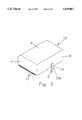
- FIG. 5is a side view of the cased devices
- FIG. 6shows four sets of cased devices on a circuit board
- FIG. 7shows the top of the circuit board with the arrayed contact pads for mounting the devices.
- FIG. 1shows a vertical surface mount device 1 which comprises an encapsulated integrated circuit memory chip having generally planar and parallel, rectangular front and rear side faces 2, 3 top left and right edges; and a plurality of contacts 11 extending out from a bottom edge 4 of the packaged device.
- Device 1is usually flow soldered onto a circuit board having a contact pad for each contact 11.
- FIG. 2shows an array 10 of nine discrete identical vertical surface mount devices 1 stacked horizontally together, side by side with their side faces 2, 3 brought into adjacent superposed relationships so that a front face 2 of one device 1 package abuts a rear face 3 of a neighboring device 1 package and so that their top, left, right and bottom edges 4 are respectively aligned in common planes, with the contacts 11 of the device packages extending respectively out of the bottom edge plane of stack 10 of the arrayed devices. More or fewer device packages may be encased, depending upon the particular application. Aligned top edges, end ones of the front and rear faces, and aligned left and right edges of the stacked device packages respectively define a top, ends and sides of the array.
- case 12is shown positioned above the horizontally arrayed device packages. Case 12 is placed over the stacked device packages and encloses them as illustrated in FIG. 3. As shown, case 12 has a generally rectangular bottom parallelepiped box-like construction, with a bottom opening internal cavity 5 (see FIG. 4) defined by internal surfaces of top, front and rear end, and right and left side walls 6, 7, 8. The dimensions of cavity 5 are chosen so that the open bottom of case 12 can be placed over the array 10, to hold the packages together by bringing the top, ends and sides of array 10 into corresponding abutment with top, end and side surfaces 6, 7, 8 of cavity 5, leaving contacts 11 exposed and accessible through the open bottom of case 12. There are two clips 13, only one shown in FIG.
- the clips 13have depending leading ends 9 which are inserted respectively into correspondingly spaced holes in a circuit board, described below, to hold the case and arrayed device packages in contact with contact pads on a circuit board.
- the clipsare made, for example from a spring-leaf material, and have a V-notch 13a for securing the clips by snap action within the holes in the circuit board.
- FIG. 4shows an end view of the arrayed packaged devices 1 in a case 12, with a portion of the case cut away to show the packaged devices in case 12.
- Contacts 11, which extend below the bottom of case 11,are in contact with circuit board 14.
- Clip 13extends through a hole in circuit board 14.
- FIG. 5is a side view of the encased array 10 of packaged devices 1.
- Case 12conforms at an angled cut-off top comer edge 12a with a correspondingly angled top edge of the stacked array 10 defined by aligned chamfered edges la of the package exteriors of devices 1, as shown in FIG. 1.
- the conforming of an angled top comer of case 12 with the corresponding aligned angled chamfered edges of the package exteriors of devices 1helps hold devices 1 in position within case 12 and presents more surface area of each device package in contact with the case. This is important since case 12 also serves as a heat sink for the cased devices.
- Case 12may be either metal or a thermally conductive plastic to assist in dissipating heat generated by the devices.
- Both clips 13are shown in FIG. 5. The two clips securely hold case 12 over packaged devices 1 against a circuit board on which the packaged devices are mounted.
- FIG. 6shows four sets of cased devices.
- each cased array 10represents a 9 ⁇ 1-Mbyte array, providing 1 Mbyte of memory.
- Eight devicesare needed to provide a 1-Mbyte ⁇ 8-bit memory array.
- Eight devices in a caseprovide the 1-Mbyte ⁇ 8-byte memory array.
- the ninth chipprovides a ninth bit for parity.
- the four cased arrays 10then provide 4 Mbytes of memory, which is commonly used in computer systems.
- FIG. 7shows the top of a circuit board 23 with contacts 32 arrayed for the four cased arrays in FIG. 6.
- each packaged devicehas 16 pins. Therefore, to provide contacts to each pin on each chip, an array of 16 ⁇ 9 contacts is needed for each cased array.
- the mounting area required by the four cased arraysis less than the space required by four SIMM modules.
- Circuit board 23has four sets of holes 24-31, one set for each 16 ⁇ 9 array of contacts. Clips 19-22 lock in holes 25-31 and another set of clips (not illustrated) lock into holes 24-30, to hold cased arrays 15-18 on circuit board 23. When the clips are locked into the holes on circuit board 23, sufficient down-pressure is exerted on the device packages to hold the device contacts in electrical contact with contact pads 32. Therefore, it is not necessary to flow solder the contacts on the devices to the contact pads on the circuit board.
Landscapes
- Engineering & Computer Science (AREA)
- Microelectronics & Electronic Packaging (AREA)
- Power Engineering (AREA)
- Physics & Mathematics (AREA)
- Condensed Matter Physics & Semiconductors (AREA)
- General Physics & Mathematics (AREA)
- Computer Hardware Design (AREA)
- Manufacturing & Machinery (AREA)
- Cooling Or The Like Of Semiconductors Or Solid State Devices (AREA)
- Coupling Device And Connection With Printed Circuit (AREA)
Abstract
Description
This invention relates to semiconductor devices, and more particularly to a system for stacking multiple semiconductor device packages in a casing and mounting the stacked packages onto a circuit board.
Memory devices used, particularly in computers, are arrayed on the computer circuit board, or mounted on small circuit boards to group encapsulated memory device packages into a distinct amount of memory capacity. For example, SIMM (Semiconductor Integrated Memory Module) devices, utilize several memory device packages interconnected on a small circuit board to form memory modules. The devices comprise integrated circuit memory chips encapsulated into discrete protective packages, with electrical connections established by soldering exposed chip contact leads onto corresponding contacts of the circuit board. The sockets into which the memory circuit boards are mounted on the computer circuit board occupy considerable space, especially if the computer is to be designed to utilize 4-Mbytes or more of memory. As computer boards become more complex, and additional functions are integrated into the computer circuit board, the space required for individual memory devices and SIMM modules needs to be reduced to accommodate other circuitry.
The invention is to an array of stacked devices utilizing vertical surface mounted semiconductor devices stacked side by side and inserting the stack of devices into a casing. The packaged stack of devices creates a cube package which is capable of replacing SIMM boards, and saves considerable space. The casing dissipates heat generated in the devices, and may be of metal or thermally conductive plastic.
The casing has two side clips which clip directly onto the circuit board on which the devices are to be mounted. The devices, which normally are attached to a circuit board by solder reflow, may be tightly clamped to contact pads on the circuit board, avoiding the necessity to solder the devices to the circuit board, and allowing the devices to be removed, when defective, without the need to remove a solder connection. Larger memory arrays are possible in a smaller space by stacking or joining a number of arrays together.
The technical advance represented by the invention as well as the objects thereof will become apparent from the following description of a preferred embodiment of the invention when considered in conjunction with the accompanying drawings, and the novel features set forth in the appended claims.
FIG. 1 illustrates a single vertical surface mount semiconductor device;
FIG. 2 shows an array f several vertical surface mount devices, and a casing for enclosing the devices;
FIG. 3 shows the encased devices;
FIG. 4 shows encased devices on a circuit board with a side cut-away showing the devices;
FIG. 5 is a side view of the cased devices;
FIG. 6 shows four sets of cased devices on a circuit board; and
FIG. 7 shows the top of the circuit board with the arrayed contact pads for mounting the devices.
FIG. 1 shows a verticalsurface mount device 1 which comprises an encapsulated integrated circuit memory chip having generally planar and parallel, rectangular front andrear side faces contacts 11 extending out from abottom edge 4 of the packaged device.Device 1 is usually flow soldered onto a circuit board having a contact pad for eachcontact 11.
FIG. 2 shows anarray 10 of nine discrete identical verticalsurface mount devices 1 stacked horizontally together, side by side with theirside faces front face 2 of onedevice 1 package abuts arear face 3 of a neighboringdevice 1 package and so that their top, left, right andbottom edges 4 are respectively aligned in common planes, with thecontacts 11 of the device packages extending respectively out of the bottom edge plane ofstack 10 of the arrayed devices. More or fewer device packages may be encased, depending upon the particular application. Aligned top edges, end ones of the front and rear faces, and aligned left and right edges of the stacked device packages respectively define a top, ends and sides of the array. Acase 12 is shown positioned above the horizontally arrayed device packages.Case 12 is placed over the stacked device packages and encloses them as illustrated in FIG. 3. As shown,case 12 has a generally rectangular bottom parallelepiped box-like construction, with a bottom opening internal cavity 5 (see FIG. 4) defined by internal surfaces of top, front and rear end, and right andleft side walls cavity 5 are chosen so that the open bottom ofcase 12 can be placed over thearray 10, to hold the packages together by bringing the top, ends and sides ofarray 10 into corresponding abutment with top, end andside surfaces cavity 5, leavingcontacts 11 exposed and accessible through the open bottom ofcase 12. There are twoclips 13, only one shown in FIG. 3, located in spaced positions, attached to respectiveopposite sides 8 ofcase 12. Theclips 13 have depending leadingends 9 which are inserted respectively into correspondingly spaced holes in a circuit board, described below, to hold the case and arrayed device packages in contact with contact pads on a circuit board. The clips are made, for example from a spring-leaf material, and have a V-notch 13a for securing the clips by snap action within the holes in the circuit board.
FIG. 4 shows an end view of the arrayed packageddevices 1 in acase 12, with a portion of the case cut away to show the packaged devices incase 12.Contacts 11, which extend below the bottom ofcase 11, are in contact withcircuit board 14.Clip 13 extends through a hole incircuit board 14.
FIG. 5 is a side view of theencased array 10 of packageddevices 1.Case 12 conforms at an angled cut-offtop comer edge 12a with a correspondingly angled top edge of thestacked array 10 defined by aligned chamfered edges la of the package exteriors ofdevices 1, as shown in FIG. 1. The conforming of an angled top comer ofcase 12 with the corresponding aligned angled chamfered edges of the package exteriors ofdevices 1 helps holddevices 1 in position withincase 12 and presents more surface area of each device package in contact with the case. This is important sincecase 12 also serves as a heat sink for the cased devices.Case 12 may be either metal or a thermally conductive plastic to assist in dissipating heat generated by the devices. Bothclips 13 are shown in FIG. 5. The two clips securely holdcase 12 over packageddevices 1 against a circuit board on which the packaged devices are mounted.
FIG. 6 shows four sets of cased devices. As an example, ifdevices 1 are 1-Mbyte memory devices, eachcased array 10 represents a 9×1-Mbyte array, providing 1 Mbyte of memory. Eight devices are needed to provide a 1-Mbyte×8-bit memory array. Eight devices in a case provide the 1-Mbyte×8-byte memory array. The ninth chip provides a ninth bit for parity. The fourcased arrays 10 then provide 4 Mbytes of memory, which is commonly used in computer systems.
FIG. 7 shows the top of acircuit board 23 withcontacts 32 arrayed for the four cased arrays in FIG. 6. In the illustrated example, each packaged device has 16 pins. Therefore, to provide contacts to each pin on each chip, an array of 16×9 contacts is needed for each cased array. In practice, the mounting area required by the four cased arrays is less than the space required by four SIMM modules.
Claims (26)
1. A system for mounting multiple packaged semiconductor devices on a circuit board, said system comprising:
a circuit board having contact pads thereon;
a plurality of discrete encapsulated vertical surface mount semiconductor device packages, each package having an exterior with front and rear side faces and top, left, fight and bottom edges, with contact leads extending out from said bottom edges; said device packages being positioned vertically and stacked horizontally in a side-by-side array with said side faces brought into adjacent superposed relationships so that a front face of one device package abuts a rear face of a neighboring device package and so that said device package top, left, right and bottom edges are respectively aligned in common planes, with the contact leads of the device packages extending out of the bottom edge common plane; said aligned top edges, end ones of said front and rear faces and aligned left and right edges of the stacked device packages respectively defining top, ends and sides of the array;
a case having a box-like construction, with an open bottom and an internal cavity defined by top, end and side internal surfaces, said case placed over said side-by-side array of device packages to bring said top, ends and sides of the array into corresponding abutment with said top, end and sides surfaces of said cavity, leaving said contact leads exposed and accessible through said case open bottom; and
means on said case, cooperative with said circuit board, releasably securing said case with said array onto said board, pressing said exposed contact leads respectively against said contact pads, establishing solderless electrical connection between said leads and said pads.
2. The system according to claim 1, wherein said case is made from a heat conducting material.
3. The system according to claim 1, wherein said means for securing comprises clips made from a spring-leaf material, and said clips have a V-notch section for locking said clips into holes insaid circuit board.
4. The system of claim 1, wherein said plurality of semiconductor device packages comprises eight identical memory chip device packages stacked together within said case cavity to form a single memory module.
5. The system of claim 4, wherein said each device package comprises 16 contact leads.
6. The system of claim 1, wherein each semiconductor device package has generally coplanar and parallel rectangular front and rear side faces; and wherein said case has a generally rectangular parallelepiped construction.
7. A system for mounting multiple packaged semiconductor devices on a circuit board, said system comprising:
a plurality of semiconductor devices, each device comprising an integrated circuit chip encapsulated into a discrete protective package and having contact leads extending out of an edge of said package, said device packages being positioned vertically in alignment in a side-by-side array;
a case having an internal cavity with an open bottom, enclosing said array of semiconductor device packages, leaving said contact leads exposed through said case open bottom;
a circuit board having contact pads thereon; and
means on said case, cooperative with said board, releasably securing said case and enclosed semiconductor device packages to said circuit board and pressing said leads respectively against said pad, establishing solderless electrical connection between said leads and said pads.
8. The system according to claim 7, wherein said array has external contour and said case internal cavity has an internal contour that conforms to said external contour; said case enclosing said array with said external contour in abutment with said internal contour.
9. The system according to claim 8, wherein said case is made from a heat conducting material.
10. The system according to claim 7, wherein said circuit board has holes and said securing means comprises clips inserted into said holes.
11. The system according to claim 10, wherein said clips are made from a spring-leaf material, and have a V-notch section for locking into said holes.
12. A system for mounting multiple packaged semiconductor devices on a circuit board, said system comprising:
a circuit board having contact pads thereon;
a plurality of discrete vertical surface mount semiconductor devices; each device comprising an integrated circuit chip encapsulated in a protective package having an exterior configuration with front and rear side faces, a bottom edge, and contact lead extending out from said bottom edge;
a case having top, end and side walls with internal surfaces defining an internal cavity with an open bottom; said plurality of semiconductor device packages being stacked into adjacent superposed relationships in an array, and held together by contact of said array with said internal surfaces of said cavity, with said bottom edges aligned so that said contact leads of said respective semiconductor devices extend out from said stack through said casing open bottom; and
means, located on said case, securing said casing to said circuit board, tightly clamping said contact leads respectively into solderless electrical connections with said contact pads.
13. The system of claim 12, wherein said semiconductor device packages are stacked in said array, with front faces of said packages positioned in abutment with rear faces of neighboring ones of said packages.
14. The system of claim 13, wherein said array has a top, ends and sides; and wherein said top, ends and sides of said array are in respective abutment with said internal surfaces of said top, ends and sides of said internal cavity.
15. The system of claim 14, wherein said exterior configurations of said semiconductor device packages further have chamfered corners; said chamfered comers are aligned in said array to form an angled edge; said case has an internal surface angled to define a corresponding angled edge of said cavity; and said angled edge of said array is in abutment with said angled edge of said cavity.
16. The system of claim 15, wherein said means for securing said case comprises at least one projection which yields elastically to lock said array-fried casing against said board.
17. The system of claim 16, wherein said at least one projection comprises at least one spring-leaf clip.
18. The system according to claim 12, wherein said means for securing comprises means for releasably securing said casing to said circuit board.
19. An electrical circuit, comprising:
a circuit board having a plurality of arrays of contact pads;
a plurality of cases, each case having top, end and side wells with internal surfaces defining an internal cavity with an open bottom;
a plurality of discrete encapsulated semiconductor device packages associated with each case; said packages each having front and rear side faces, a bottom edge, and contact leads extending from said bottom edge; and the packages of each of said plurality of packages being stacked vertically in side-by-side relationships within the respective internal cavity of each case, each case holding said packages in an array with said front and rear side faces in superposed relationships and said bottom edges aligned to present said bottom edges of the respective packages of each case in generally planar alignment and said associated contact leads exposed in an array at said open bottom; and
means, associated with each case, securing each case to said circuit board, clamping said packages against, said board to establish solderless electrical connections between contact leads of said contact arrays and respective pads of said contact pad arrays.
20. The electrical circuit of claim 19, wherein said board includes a receptacle adjacent each contact pad array, and said means for securing, comprises a clip on each casing having a leading end inserted within said receptacle.
21. The electrical circuit of claim 20, wherein said receptacle is a hole; said clip is a resilient member that can be snapped into said hole; and said cases, semiconductor devices, and circuit board are relatively dimensioned and configured so that when said dips are mapped into said holes, said contacts are clamped against said pads.
22. A system for packaging and mounting a plurality of semiconductor devices, comprising:
a circuit board with contact pads;
a plurality of discrete vertical surface mount semiconductor devices; each device having front and rear side faces, a bottom edge, and contact leads extending out from said bottom edge;
a case having top, end and side walls with internal surfaces defining an internal cavity with an open bottom; said plurality of discrete semiconductor devices being stacked side by side within said cavity to form an array matching said internal surfaces, said front and rear faces brought into adjacent superposed relationships, with front faces of ones of said devices positioned in abutment with rear faces of neighboring ones of said devices, and said bottom edges aligned so that said contact leads of said respective semiconductor devices extend out from said stack through said case open bottom; and
means, located on said case, for securing said case to said circuit board to hold said array within said cavity and clamp said contact leads into respective solderless electrical connections with said contact pads.
23. The system of claim 22, wherein said semiconductor devices further have chamfered corners; said chamfered corners are aligned in said array to form an angled edge; said case has an internal surface angled to define a corresponding angled edge of said cavity; and said angled edge of said array is in abutment with said angled edge of said cavity.
24. The system of claim 23, wherein said circuit board has at least one, receptacle; and said means for securing said case comprises at least one projection which yields elastically to lock said projection within said at least one receptacle.
25. The system of claim 24, wherein said at least one receptacle comprises at least one hole; and said at least one projection comprises at least one spring leaf clip.
26. A semiconductor package system for mounting an array of multiple devices comprising:
a circuit board having contact pads;
a plurality of discrete vertical surface mount semiconductor device packages having front and rear side faces and bottom edges with contact leads extending out from said bottom edges; said device packages being positioned in a side-by-side array with said side faces in adjacent superposed relationships and said bottom edges aligned in a common plane; said array having external contour;
a case having an internal cavity with an internal contour that conforms to said array external contour; said internal cavity enclosing said array of discrete semiconductor device packages and having an opening leaving said contact leads exposed; and
means on said case, cooperative with said board, clamping said array within said cavity against said board pressing said exposed contact leads against said pads to establish respective solderless electrical connections between said leads and said pads.
Priority Applications (2)
| Application Number | Priority Date | Filing Date | Title |
|---|---|---|---|
| US08/236,768US5619067A (en) | 1994-05-02 | 1994-05-02 | Semiconductor device package side-by-side stacking and mounting system |
| US08/586,366US5663105A (en) | 1994-05-02 | 1996-01-16 | Semiconductor device package side-by-side stacking and mounting system |
Applications Claiming Priority (1)
| Application Number | Priority Date | Filing Date | Title |
|---|---|---|---|
| US08/236,768US5619067A (en) | 1994-05-02 | 1994-05-02 | Semiconductor device package side-by-side stacking and mounting system |
Related Child Applications (1)
| Application Number | Title | Priority Date | Filing Date |
|---|---|---|---|
| US48522795AContinuation | 1994-05-02 | 1995-06-07 |
Publications (1)
| Publication Number | Publication Date |
|---|---|
| US5619067Atrue US5619067A (en) | 1997-04-08 |
Family
ID=22890875
Family Applications (2)
| Application Number | Title | Priority Date | Filing Date |
|---|---|---|---|
| US08/236,768Expired - LifetimeUS5619067A (en) | 1994-05-02 | 1994-05-02 | Semiconductor device package side-by-side stacking and mounting system |
| US08/586,366Expired - LifetimeUS5663105A (en) | 1994-05-02 | 1996-01-16 | Semiconductor device package side-by-side stacking and mounting system |
Family Applications After (1)
| Application Number | Title | Priority Date | Filing Date |
|---|---|---|---|
| US08/586,366Expired - LifetimeUS5663105A (en) | 1994-05-02 | 1996-01-16 | Semiconductor device package side-by-side stacking and mounting system |
Country Status (1)
| Country | Link |
|---|---|
| US (2) | US5619067A (en) |
Cited By (16)
| Publication number | Priority date | Publication date | Assignee | Title |
|---|---|---|---|---|
| US5892287A (en)* | 1997-08-18 | 1999-04-06 | Texas Instruments | Semiconductor device including stacked chips having metal patterned on circuit surface and on edge side of chip |
| US5910682A (en)* | 1996-06-17 | 1999-06-08 | Lg Semicon Co., Ltd. | Semiconductor chip stack package |
| US5956236A (en)* | 1997-11-25 | 1999-09-21 | Micron Technology, Inc. | Integrated circuit package support system |
| US6089920A (en)* | 1998-05-04 | 2000-07-18 | Micron Technology, Inc. | Modular die sockets with flexible interconnects for packaging bare semiconductor die |
| US6093029A (en)* | 1998-09-08 | 2000-07-25 | S3 Incorporated | Vertically stackable integrated circuit |
| US6140696A (en)* | 1998-01-27 | 2000-10-31 | Micron Technology, Inc. | Vertically mountable semiconductor device and methods |
| US6151220A (en)* | 1997-06-30 | 2000-11-21 | Oki Electric Industry Co., Ltd. | Mounting structure for electronic part |
| US6265773B1 (en) | 1997-12-31 | 2001-07-24 | Micron Technology, Inc. | Vertically mountable and alignable semiconductor device, assembly, and methods |
| US6326687B1 (en)* | 1998-09-01 | 2001-12-04 | Micron Technology, Inc. | IC package with dual heat spreaders |
| KR20020028017A (en)* | 2000-10-06 | 2002-04-15 | 박종섭 | High density package |
| US20040084211A1 (en)* | 2002-10-30 | 2004-05-06 | Sensonix, Inc. | Z-axis packaging for electronic device and method for making same |
| US20040164406A1 (en)* | 2003-02-26 | 2004-08-26 | Chih-Liang Hu | Discrete circuit component having an up-right circuit die with lateral electrical connections |
| US6995412B2 (en) | 2002-04-12 | 2006-02-07 | International Business Machines Corporation | Integrated circuit with capacitors having a fin structure |
| US20070120243A1 (en)* | 2000-06-07 | 2007-05-31 | Sony Corporation | Assembly jig and manufacturing method of multilayer semiconductor device |
| US8900503B2 (en) | 2011-09-28 | 2014-12-02 | International Business Machines Corporation | Method of forming an overmolded dual in-line memory module cooling structure |
| CN113068333A (en)* | 2015-09-15 | 2021-07-02 | 赛峰电子与防务公司 | Compact electronic system and device comprising such a system |
Families Citing this family (26)
| Publication number | Priority date | Publication date | Assignee | Title |
|---|---|---|---|---|
| US6008074A (en)* | 1998-10-01 | 1999-12-28 | Micron Technology, Inc. | Method of forming a synchronous-link dynamic random access memory edge-mounted device |
| FR2797348B1 (en)* | 1999-08-02 | 2001-10-19 | Cit Alcatel | METHOD FOR OBTAINING A HIGH DENSITY MODULE FROM ELECTRONIC, MODULAR, ENCAPSULATED COMPONENTS AND MODULE THUS OBTAINED |
| KR100725942B1 (en)* | 2001-03-16 | 2007-06-11 | 삼성전자주식회사 | Stacked Vertical In-Line Packages |
| SG139508A1 (en)* | 2001-09-10 | 2008-02-29 | Micron Technology Inc | Wafer dicing device and method |
| SG102639A1 (en)* | 2001-10-08 | 2004-03-26 | Micron Technology Inc | Apparatus and method for packing circuits |
| SG142115A1 (en) | 2002-06-14 | 2008-05-28 | Micron Technology Inc | Wafer level packaging |
| SG119185A1 (en) | 2003-05-06 | 2006-02-28 | Micron Technology Inc | Method for packaging circuits and packaged circuits |
| US9495285B2 (en) | 2014-09-16 | 2016-11-15 | Integrated Device Technology, Inc. | Initiating operation of a timing device using a read only memory (ROM) or a one time programmable non volatile memory (OTP NVM) |
| US9553570B1 (en) | 2014-12-10 | 2017-01-24 | Integrated Device Technology, Inc. | Crystal-less jitter attenuator |
| US9369139B1 (en) | 2015-02-14 | 2016-06-14 | Integrated Device Technology, Inc. | Fractional reference-injection PLL |
| US9336896B1 (en) | 2015-03-23 | 2016-05-10 | Integrated Device Technology, Inc. | System and method for voltage regulation of one-time-programmable (OTP) memory programming voltage |
| US9455045B1 (en) | 2015-04-20 | 2016-09-27 | Integrated Device Technology, Inc. | Controlling operation of a timing device using an OTP NVM to store timing device configurations in a RAM |
| US9362928B1 (en) | 2015-07-08 | 2016-06-07 | Integrated Device Technology, Inc. | Low-spurious fractional N-frequency divider and method of use |
| US9954516B1 (en) | 2015-08-19 | 2018-04-24 | Integrated Device Technology, Inc. | Timing device having multi-purpose pin with proactive function |
| US9590637B1 (en) | 2015-08-28 | 2017-03-07 | Integrated Device Technology, Inc. | High-speed programmable frequency divider with 50% output duty cycle |
| US9847869B1 (en) | 2015-10-23 | 2017-12-19 | Integrated Device Technology, Inc. | Frequency synthesizer with microcode control |
| US9614508B1 (en) | 2015-12-03 | 2017-04-04 | Integrated Device Technology, Inc. | System and method for deskewing output clock signals |
| US10075284B1 (en) | 2016-01-21 | 2018-09-11 | Integrated Device Technology, Inc. | Pulse width modulation (PWM) to align clocks across multiple separated cards within a communication system |
| US9852039B1 (en) | 2016-02-03 | 2017-12-26 | Integrated Device Technology, Inc | Phase locked loop (PLL) timing device evaluation system and method for evaluating PLL timing devices |
| US9859901B1 (en) | 2016-03-08 | 2018-01-02 | Integrated Device Technology, Inc. | Buffer with programmable input/output phase relationship |
| US9692394B1 (en) | 2016-03-25 | 2017-06-27 | Integrated Device Technology, Inc. | Programmable low power high-speed current steering logic (LPHCSL) driver and method of use |
| US9698787B1 (en) | 2016-03-28 | 2017-07-04 | Integrated Device Technology, Inc. | Integrated low voltage differential signaling (LVDS) and high-speed current steering logic (HCSL) circuit and method of use |
| US9954541B1 (en) | 2016-03-29 | 2018-04-24 | Integrated Device Technology, Inc. | Bulk acoustic wave resonator based fractional frequency synthesizer and method of use |
| US9581973B1 (en) | 2016-03-29 | 2017-02-28 | Integrated Device Technology, Inc. | Dual mode clock using a common resonator and associated method of use |
| US9654121B1 (en) | 2016-06-01 | 2017-05-16 | Integrated Device Technology, Inc. | Calibration method and apparatus for phase locked loop circuit |
| WO2018018163A2 (en)* | 2016-07-29 | 2018-02-01 | Adc Technologies Inc. | Fanless rail cooled electronics apparatus |
Citations (13)
| Publication number | Priority date | Publication date | Assignee | Title |
|---|---|---|---|---|
| JPS61248451A (en)* | 1985-04-26 | 1986-11-05 | Hitachi Ltd | Package sealing structure for semiconductor devices |
| US4656605A (en)* | 1983-09-02 | 1987-04-07 | Wang Laboratories, Inc. | Single in-line memory module |
| US4667270A (en)* | 1984-10-31 | 1987-05-19 | Kitagawa Industries Co., Ltd. | Light emitting diode holder |
| US4706166A (en)* | 1986-04-25 | 1987-11-10 | Irvine Sensors Corporation | High-density electronic modules--process and product |
| JPH01274479A (en)* | 1988-04-26 | 1989-11-02 | Mitsubishi Electric Corp | Optical input integrated circuit device |
| US4975763A (en)* | 1988-03-14 | 1990-12-04 | Texas Instruments Incorporated | Edge-mounted, surface-mount package for semiconductor integrated circuit devices |
| US5109317A (en)* | 1989-11-07 | 1992-04-28 | Hitachi, Ltd. | Mounting mechanism for mounting heat sink on multi-chip module |
| JPH04132250A (en)* | 1990-09-21 | 1992-05-06 | Nec Corp | Ic package for solderless mounting |
| US5279029A (en)* | 1990-08-01 | 1994-01-18 | Staktek Corporation | Ultra high density integrated circuit packages method |
| US5349235A (en)* | 1992-09-08 | 1994-09-20 | Samsung Electronics Co., Ltd. | High density vertically mounted semiconductor package |
| US5362986A (en)* | 1993-08-19 | 1994-11-08 | International Business Machines Corporation | Vertical chip mount memory package with packaging substrate and memory chip pairs |
| USRE34794E (en)* | 1989-11-06 | 1994-11-22 | Micron Technology, Inc. | Gull-wing zig-zag inline lead package having end-of-package anchoring pins |
| US5413970A (en)* | 1993-10-08 | 1995-05-09 | Texas Instruments Incorporated | Process for manufacturing a semiconductor package having two rows of interdigitated leads |
- 1994
- 1994-05-02USUS08/236,768patent/US5619067A/ennot_activeExpired - Lifetime
- 1996
- 1996-01-16USUS08/586,366patent/US5663105A/ennot_activeExpired - Lifetime
Patent Citations (13)
| Publication number | Priority date | Publication date | Assignee | Title |
|---|---|---|---|---|
| US4656605A (en)* | 1983-09-02 | 1987-04-07 | Wang Laboratories, Inc. | Single in-line memory module |
| US4667270A (en)* | 1984-10-31 | 1987-05-19 | Kitagawa Industries Co., Ltd. | Light emitting diode holder |
| JPS61248451A (en)* | 1985-04-26 | 1986-11-05 | Hitachi Ltd | Package sealing structure for semiconductor devices |
| US4706166A (en)* | 1986-04-25 | 1987-11-10 | Irvine Sensors Corporation | High-density electronic modules--process and product |
| US4975763A (en)* | 1988-03-14 | 1990-12-04 | Texas Instruments Incorporated | Edge-mounted, surface-mount package for semiconductor integrated circuit devices |
| JPH01274479A (en)* | 1988-04-26 | 1989-11-02 | Mitsubishi Electric Corp | Optical input integrated circuit device |
| USRE34794E (en)* | 1989-11-06 | 1994-11-22 | Micron Technology, Inc. | Gull-wing zig-zag inline lead package having end-of-package anchoring pins |
| US5109317A (en)* | 1989-11-07 | 1992-04-28 | Hitachi, Ltd. | Mounting mechanism for mounting heat sink on multi-chip module |
| US5279029A (en)* | 1990-08-01 | 1994-01-18 | Staktek Corporation | Ultra high density integrated circuit packages method |
| JPH04132250A (en)* | 1990-09-21 | 1992-05-06 | Nec Corp | Ic package for solderless mounting |
| US5349235A (en)* | 1992-09-08 | 1994-09-20 | Samsung Electronics Co., Ltd. | High density vertically mounted semiconductor package |
| US5362986A (en)* | 1993-08-19 | 1994-11-08 | International Business Machines Corporation | Vertical chip mount memory package with packaging substrate and memory chip pairs |
| US5413970A (en)* | 1993-10-08 | 1995-05-09 | Texas Instruments Incorporated | Process for manufacturing a semiconductor package having two rows of interdigitated leads |
Cited By (61)
| Publication number | Priority date | Publication date | Assignee | Title |
|---|---|---|---|---|
| US5910682A (en)* | 1996-06-17 | 1999-06-08 | Lg Semicon Co., Ltd. | Semiconductor chip stack package |
| US6151220A (en)* | 1997-06-30 | 2000-11-21 | Oki Electric Industry Co., Ltd. | Mounting structure for electronic part |
| US6033931A (en)* | 1997-08-18 | 2000-03-07 | Texas Instruments Incorporated | Semiconductor device including stacked chips having metal patterned on circuit surface and one edge side of chip |
| US5892287A (en)* | 1997-08-18 | 1999-04-06 | Texas Instruments | Semiconductor device including stacked chips having metal patterned on circuit surface and on edge side of chip |
| US20100148334A1 (en)* | 1997-11-25 | 2010-06-17 | Micron Technology, Inc. | Intergrated circuit package support system |
| US5956236A (en)* | 1997-11-25 | 1999-09-21 | Micron Technology, Inc. | Integrated circuit package support system |
| US8035974B1 (en) | 1997-11-25 | 2011-10-11 | Round Rock Research, Llc | Integrated circuit package support system |
| US7894192B2 (en) | 1997-11-25 | 2011-02-22 | Round Rock Research, Llc | Integrated circuit package support system |
| US20060001150A1 (en)* | 1997-12-31 | 2006-01-05 | Kinsman Larry D | Alignment devices for securing semiconductor devices to carrier substrates, and assemblies including the alignment devices |
| US20060030072A1 (en)* | 1997-12-31 | 2006-02-09 | Kinsman Larry D | Methods for securing packaged semiconductor devices to carrier substrates |
| US20030196323A1 (en)* | 1997-12-31 | 2003-10-23 | Kinsman Larry D. | Methods for modifying a vertical surface mount package |
| US7569418B2 (en) | 1997-12-31 | 2009-08-04 | Micron Technology, Inc. | Methods for securing packaged semiconductor devices to carrier substrates |
| US6342731B1 (en) | 1997-12-31 | 2002-01-29 | Micron Technology, Inc. | Vertically mountable semiconductor device, assembly, and methods |
| US7082681B2 (en) | 1997-12-31 | 2006-08-01 | Micron Technology, Inc. | Methods for modifying a vertical surface mount package |
| US6634098B1 (en) | 1997-12-31 | 2003-10-21 | Micron Technology, Inc. | Methods for assembling, modifying and manufacturing a vertical surface mount package |
| US6963128B2 (en) | 1997-12-31 | 2005-11-08 | Micron Technology, Inc. | Vertically mountable and alignable semiconductor device assembly |
| US20060033190A1 (en)* | 1997-12-31 | 2006-02-16 | Kinsman Larry D | Vertically mountable and alignable semiconductor device packages and assemblies including the same |
| US6265773B1 (en) | 1997-12-31 | 2001-07-24 | Micron Technology, Inc. | Vertically mountable and alignable semiconductor device, assembly, and methods |
| US20030111718A1 (en)* | 1997-12-31 | 2003-06-19 | Kinsman Larry D. | Vertically mountable and alignable semiconductor device assembly |
| US6512290B2 (en) | 1997-12-31 | 2003-01-28 | Micron Technology, Inc. | Vertically mountable and alignable semiconductor device, assembly, and methods |
| US20060001155A1 (en)* | 1997-12-31 | 2006-01-05 | Kinsman Larry D | Semiconductor device packages including leads with substantially planar exposed portions extending from bottom edges of the packages, and assemblies including the packages |
| US6531764B2 (en) | 1997-12-31 | 2003-03-11 | Micron Technology, Inc. | Vertically mountable semiconductor device, assembly, and methods |
| US6800942B1 (en) | 1998-01-27 | 2004-10-05 | Micron Technology, Inc. | Vertically mountable semiconductor device and methods |
| US6140696A (en)* | 1998-01-27 | 2000-10-31 | Micron Technology, Inc. | Vertically mountable semiconductor device and methods |
| US6383839B2 (en) | 1998-01-27 | 2002-05-07 | Micron Technology, Inc. | Vertically mountable semiconductor device and methods |
| US6239012B1 (en) | 1998-01-27 | 2001-05-29 | Micron Technology, Inc. | Vertically mountable semiconductor device and methods |
| US7040930B2 (en) | 1998-05-04 | 2006-05-09 | Micron Technology, Inc. | Modular sockets using flexible interconnects |
| US6453550B1 (en) | 1998-05-04 | 2002-09-24 | Micron Technology, Inc. | Method for forming modular sockets using flexible interconnects and resulting structures |
| US6758696B2 (en) | 1998-05-04 | 2004-07-06 | Micron Technology, Inc. | Method and apparatus for forming modular sockets using flexible interconnects and resulting structures |
| US6760970B2 (en) | 1998-05-04 | 2004-07-13 | Micron Technology, Inc. | Method for forming modular sockets using flexible interconnects and resulting structures |
| US6089920A (en)* | 1998-05-04 | 2000-07-18 | Micron Technology, Inc. | Modular die sockets with flexible interconnects for packaging bare semiconductor die |
| US6319065B1 (en) | 1998-05-04 | 2001-11-20 | Micron Technology, Inc. | Method and apparatus for forming modular sockets using flexible interconnects and resulting structures |
| US7367845B2 (en) | 1998-05-04 | 2008-05-06 | Micron Technology, Inc. | Modular sockets using flexible interconnects |
| US7192311B2 (en) | 1998-05-04 | 2007-03-20 | Micron Technology, Inc. | Apparatus for forming modular sockets using flexible interconnects and resulting structures |
| US20050142954A1 (en)* | 1998-05-04 | 2005-06-30 | Farnworth Warren M. | Modular sockets using flexible interconnects |
| US6751859B2 (en) | 1998-05-04 | 2004-06-22 | Micron Technology, Inc. | Method for forming modular sockets using flexible interconnects and resulting structures |
| US6612872B2 (en) | 1998-05-04 | 2003-09-02 | Micron Technology, Inc. | Apparatus for forming modular sockets using flexible interconnects and resulting structures |
| US20050269686A1 (en)* | 1998-05-04 | 2005-12-08 | Farnworth Warren M | Method and apparatus for forming modular sockets using flexible interconnects and resulting structures |
| US20070059984A1 (en)* | 1998-05-04 | 2007-03-15 | Farnworth Warren M | Modular sockets using flexible interconnects |
| US7153164B2 (en) | 1998-05-04 | 2006-12-26 | Micron Technology, Inc. | Method and apparatus for forming modular sockets using flexible interconnects and resulting structures |
| US20060234560A1 (en)* | 1998-05-04 | 2006-10-19 | Farnworth Warren M | Modular sockets using flexible interconnects |
| US7094108B2 (en) | 1998-05-04 | 2006-08-22 | Micron Technology, Inc. | Apparatus for forming modular sockets using flexible interconnects and resulting structures |
| US6478627B2 (en) | 1998-05-04 | 2002-11-12 | Micron Technology, Inc. | Method and apparatus for forming modular sockets using flexible interconnects and resulting structures |
| US6920688B2 (en) | 1998-09-01 | 2005-07-26 | Micron Technology, Inc. | Method for a semiconductor assembly having a semiconductor die with dual heat spreaders |
| US6518098B2 (en) | 1998-09-01 | 2003-02-11 | Micron Technology, Inc. | IC package with dual heat spreaders |
| US6765291B2 (en) | 1998-09-01 | 2004-07-20 | Micron Technology, Inc. | IC package with dual heat spreaders |
| US20020185727A1 (en)* | 1998-09-01 | 2002-12-12 | Corisis David J. | IC package with dual heat spreaders |
| US6326687B1 (en)* | 1998-09-01 | 2001-12-04 | Micron Technology, Inc. | IC package with dual heat spreaders |
| US20030000082A1 (en)* | 1998-09-01 | 2003-01-02 | Corisis David J. | IC package with dual heat spreaders |
| US6093029A (en)* | 1998-09-08 | 2000-07-25 | S3 Incorporated | Vertically stackable integrated circuit |
| US20070120243A1 (en)* | 2000-06-07 | 2007-05-31 | Sony Corporation | Assembly jig and manufacturing method of multilayer semiconductor device |
| KR20020028017A (en)* | 2000-10-06 | 2002-04-15 | 박종섭 | High density package |
| US20060038216A1 (en)* | 2002-04-12 | 2006-02-23 | Fried David M | Formation of capacitor having a Fin structure |
| US6995412B2 (en) | 2002-04-12 | 2006-02-07 | International Business Machines Corporation | Integrated circuit with capacitors having a fin structure |
| US7060553B2 (en) | 2002-04-12 | 2006-06-13 | International Business Machines Corporation | Formation of capacitor having a Fin structure |
| US20040084211A1 (en)* | 2002-10-30 | 2004-05-06 | Sensonix, Inc. | Z-axis packaging for electronic device and method for making same |
| US6870261B2 (en)* | 2003-02-26 | 2005-03-22 | Comchip Technology Co., Ltd. | Discrete circuit component having an up-right circuit die with lateral electrical connections |
| US20040164406A1 (en)* | 2003-02-26 | 2004-08-26 | Chih-Liang Hu | Discrete circuit component having an up-right circuit die with lateral electrical connections |
| US8900503B2 (en) | 2011-09-28 | 2014-12-02 | International Business Machines Corporation | Method of forming an overmolded dual in-line memory module cooling structure |
| US9943936B2 (en) | 2011-09-28 | 2018-04-17 | Lenovo Enterprise Solutions (Singapore) Pte. Ltd. | Overmolded dual in-line memory module cooling structure |
| CN113068333A (en)* | 2015-09-15 | 2021-07-02 | 赛峰电子与防务公司 | Compact electronic system and device comprising such a system |
Also Published As
| Publication number | Publication date |
|---|---|
| US5663105A (en) | 1997-09-02 |
Similar Documents
| Publication | Publication Date | Title |
|---|---|---|
| US5619067A (en) | Semiconductor device package side-by-side stacking and mounting system | |
| EP1264347B1 (en) | Electronic module having a three dimensional array of carrier-mounted integrated circuit packages | |
| EP0555659B1 (en) | Multi-chip Module | |
| US5276585A (en) | Heat sink mounting apparatus | |
| EP0157147B1 (en) | Stacked double density memory module using industry standard memory chips, double density memory board and method of forming a stacked double density memory module | |
| US6713854B1 (en) | Electronic circuit module with a carrier having a mounting pad array | |
| US5708297A (en) | Thin multichip module | |
| EP1327265B1 (en) | Electronic module having canopy-type carriers | |
| GB2283781A (en) | Spring clamp assembly with electrically insulating shoe | |
| US5671121A (en) | Kangaroo multi-package interconnection concept | |
| US6734529B2 (en) | Vertically mountable interposer and assembly | |
| US5790381A (en) | Integrated circuit package assembly | |
| US4629267A (en) | Circuit terminating device | |
| US5623395A (en) | Integrated circuit package assembly | |
| US5014114A (en) | High speed, high density semiconductor memory package with chip level repairability | |
| US20020112871A1 (en) | Compact stacked electronic package | |
| JP2571021B2 (en) | Connection adapter and mounting structure for semiconductor device | |
| CA2031865A1 (en) | High-density memory array packaging | |
| EP0220460B1 (en) | Stacked module using standard integrated circuit chips | |
| EP0167538A1 (en) | Flat package for integrated circuit memory chips. | |
| CA1256175A (en) | Circuit to post interconnection device |
Legal Events
| Date | Code | Title | Description |
|---|---|---|---|
| AS | Assignment | Owner name:TEXAS INSTRUMENTS INCORPORATED, TEXAS Free format text:ASSIGNMENT OF ASSIGNORS INTEREST;ASSIGNORS:SUA, GOH JING;YU, CHAN MIN;REEL/FRAME:006996/0580 Effective date:19940420 | |
| STCF | Information on status: patent grant | Free format text:PATENTED CASE | |
| FPAY | Fee payment | Year of fee payment:4 | |
| FPAY | Fee payment | Year of fee payment:8 | |
| FPAY | Fee payment | Year of fee payment:12 |