US5617991A - Method for electrically conductive metal-to-metal bonding - Google Patents
Method for electrically conductive metal-to-metal bondingDownload PDFInfo
- Publication number
- US5617991A US5617991AUS08/566,070US56607095AUS5617991AUS 5617991 AUS5617991 AUS 5617991AUS 56607095 AUS56607095 AUS 56607095AUS 5617991 AUS5617991 AUS 5617991A
- Authority
- US
- United States
- Prior art keywords
- metal
- aluminum
- titanium
- inert
- ambiance
- Prior art date
- Legal status (The legal status is an assumption and is not a legal conclusion. Google has not performed a legal analysis and makes no representation as to the accuracy of the status listed.)
- Expired - Lifetime
Links
- 229910052751metalInorganic materials0.000titleclaimsabstractdescription92
- 239000002184metalSubstances0.000titleclaimsabstractdescription92
- 238000000034methodMethods0.000titleclaimsabstractdescription44
- 239000010936titaniumSubstances0.000claimsabstractdescription52
- RTAQQCXQSZGOHL-UHFFFAOYSA-NTitaniumChemical compound[Ti]RTAQQCXQSZGOHL-UHFFFAOYSA-N0.000claimsabstractdescription51
- 229910052719titaniumInorganic materials0.000claimsabstractdescription51
- 238000000151depositionMethods0.000claimsabstractdescription16
- 238000010438heat treatmentMethods0.000claimsabstractdescription12
- 230000008018meltingEffects0.000claimsabstractdescription8
- 238000002844meltingMethods0.000claimsabstractdescription8
- 229910052782aluminiumInorganic materials0.000claimsdescription83
- XAGFODPZIPBFFR-UHFFFAOYSA-NaluminiumChemical compound[Al]XAGFODPZIPBFFR-UHFFFAOYSA-N0.000claimsdescription80
- 229910052710siliconInorganic materials0.000claimsdescription44
- 239000010703siliconSubstances0.000claimsdescription44
- XKRFYHLGVUSROY-UHFFFAOYSA-NArgonChemical compound[Ar]XKRFYHLGVUSROY-UHFFFAOYSA-N0.000claimsdescription14
- IJGRMHOSHXDMSA-UHFFFAOYSA-NAtomic nitrogenChemical compoundN#NIJGRMHOSHXDMSA-UHFFFAOYSA-N0.000claimsdescription14
- 229910052786argonInorganic materials0.000claimsdescription7
- 229910052757nitrogenInorganic materials0.000claimsdescription7
- RYGMFSIKBFXOCR-UHFFFAOYSA-NCopperChemical compound[Cu]RYGMFSIKBFXOCR-UHFFFAOYSA-N0.000claimsdescription4
- 229910052802copperInorganic materials0.000claimsdescription4
- 239000010949copperSubstances0.000claimsdescription4
- 235000012431wafersNutrition0.000description87
- XUIMIQQOPSSXEZ-UHFFFAOYSA-NSiliconChemical compound[Si]XUIMIQQOPSSXEZ-UHFFFAOYSA-N0.000description42
- 239000000758substrateSubstances0.000description26
- VYPSYNLAJGMNEJ-UHFFFAOYSA-NSilicium dioxideChemical compoundO=[Si]=OVYPSYNLAJGMNEJ-UHFFFAOYSA-N0.000description12
- 238000010586diagramMethods0.000description12
- 229910052814silicon oxideInorganic materials0.000description12
- 150000002739metalsChemical class0.000description10
- 230000008901benefitEffects0.000description9
- 229910000679solderInorganic materials0.000description7
- 238000009413insulationMethods0.000description6
- 229910000765intermetallicInorganic materials0.000description6
- 238000001465metallisationMethods0.000description6
- 230000008569processEffects0.000description6
- 238000000137annealingMethods0.000description4
- 230000008021depositionEffects0.000description4
- 229910000838Al alloyInorganic materials0.000description3
- 229910010039TiAl3Inorganic materials0.000description3
- QVGXLLKOCUKJST-UHFFFAOYSA-Natomic oxygenChemical compound[O]QVGXLLKOCUKJST-UHFFFAOYSA-N0.000description3
- 230000008878couplingEffects0.000description3
- 238000010168coupling processMethods0.000description3
- 238000005859coupling reactionMethods0.000description3
- 238000005516engineering processMethods0.000description3
- 239000001301oxygenSubstances0.000description3
- 229910052760oxygenInorganic materials0.000description3
- 238000000059patterningMethods0.000description3
- 230000007547defectEffects0.000description2
- 230000003647oxidationEffects0.000description2
- 238000007254oxidation reactionMethods0.000description2
- 238000005240physical vapour depositionMethods0.000description2
- 239000000853adhesiveSubstances0.000description1
- 230000001070adhesive effectEffects0.000description1
- 239000003990capacitorSubstances0.000description1
- 230000015556catabolic processEffects0.000description1
- 238000006731degradation reactionMethods0.000description1
- 238000005137deposition processMethods0.000description1
- 230000000694effectsEffects0.000description1
- 238000004519manufacturing processMethods0.000description1
- 238000012986modificationMethods0.000description1
- 230000004048modificationEffects0.000description1
- TWNQGVIAIRXVLR-UHFFFAOYSA-Noxo(oxoalumanyloxy)alumaneChemical compoundO=[Al]O[Al]=OTWNQGVIAIRXVLR-UHFFFAOYSA-N0.000description1
- 230000003071parasitic effectEffects0.000description1
- 238000004544sputter depositionMethods0.000description1
- 238000002207thermal evaporationMethods0.000description1
Images


Classifications
- H—ELECTRICITY
- H01—ELECTRIC ELEMENTS
- H01L—SEMICONDUCTOR DEVICES NOT COVERED BY CLASS H10
- H01L24/00—Arrangements for connecting or disconnecting semiconductor or solid-state bodies; Methods or apparatus related thereto
- H01L24/01—Means for bonding being attached to, or being formed on, the surface to be connected, e.g. chip-to-package, die-attach, "first-level" interconnects; Manufacturing methods related thereto
- H01L24/26—Layer connectors, e.g. plate connectors, solder or adhesive layers; Manufacturing methods related thereto
- H01L24/31—Structure, shape, material or disposition of the layer connectors after the connecting process
- H—ELECTRICITY
- H01—ELECTRIC ELEMENTS
- H01L—SEMICONDUCTOR DEVICES NOT COVERED BY CLASS H10
- H01L24/00—Arrangements for connecting or disconnecting semiconductor or solid-state bodies; Methods or apparatus related thereto
- H01L24/01—Means for bonding being attached to, or being formed on, the surface to be connected, e.g. chip-to-package, die-attach, "first-level" interconnects; Manufacturing methods related thereto
- H01L24/26—Layer connectors, e.g. plate connectors, solder or adhesive layers; Manufacturing methods related thereto
- H01L24/28—Structure, shape, material or disposition of the layer connectors prior to the connecting process
- H—ELECTRICITY
- H01—ELECTRIC ELEMENTS
- H01L—SEMICONDUCTOR DEVICES NOT COVERED BY CLASS H10
- H01L24/00—Arrangements for connecting or disconnecting semiconductor or solid-state bodies; Methods or apparatus related thereto
- H01L24/80—Methods for connecting semiconductor or other solid state bodies using means for bonding being attached to, or being formed on, the surface to be connected
- H01L24/83—Methods for connecting semiconductor or other solid state bodies using means for bonding being attached to, or being formed on, the surface to be connected using a layer connector
- H—ELECTRICITY
- H01—ELECTRIC ELEMENTS
- H01L—SEMICONDUCTOR DEVICES NOT COVERED BY CLASS H10
- H01L25/00—Assemblies consisting of a plurality of semiconductor or other solid state devices
- H01L25/50—Multistep manufacturing processes of assemblies consisting of devices, the devices being individual devices of subclass H10D or integrated devices of class H10
- H—ELECTRICITY
- H01—ELECTRIC ELEMENTS
- H01L—SEMICONDUCTOR DEVICES NOT COVERED BY CLASS H10
- H01L2224/00—Indexing scheme for arrangements for connecting or disconnecting semiconductor or solid-state bodies and methods related thereto as covered by H01L24/00
- H01L2224/01—Means for bonding being attached to, or being formed on, the surface to be connected, e.g. chip-to-package, die-attach, "first-level" interconnects; Manufacturing methods related thereto
- H01L2224/02—Bonding areas; Manufacturing methods related thereto
- H01L2224/04—Structure, shape, material or disposition of the bonding areas prior to the connecting process
- H01L2224/04026—Bonding areas specifically adapted for layer connectors
- H—ELECTRICITY
- H01—ELECTRIC ELEMENTS
- H01L—SEMICONDUCTOR DEVICES NOT COVERED BY CLASS H10
- H01L2224/00—Indexing scheme for arrangements for connecting or disconnecting semiconductor or solid-state bodies and methods related thereto as covered by H01L24/00
- H01L2224/80—Methods for connecting semiconductor or other solid state bodies using means for bonding being attached to, or being formed on, the surface to be connected
- H01L2224/83—Methods for connecting semiconductor or other solid state bodies using means for bonding being attached to, or being formed on, the surface to be connected using a layer connector
- H01L2224/8319—Arrangement of the layer connectors prior to mounting
- H—ELECTRICITY
- H01—ELECTRIC ELEMENTS
- H01L—SEMICONDUCTOR DEVICES NOT COVERED BY CLASS H10
- H01L2224/00—Indexing scheme for arrangements for connecting or disconnecting semiconductor or solid-state bodies and methods related thereto as covered by H01L24/00
- H01L2224/80—Methods for connecting semiconductor or other solid state bodies using means for bonding being attached to, or being formed on, the surface to be connected
- H01L2224/83—Methods for connecting semiconductor or other solid state bodies using means for bonding being attached to, or being formed on, the surface to be connected using a layer connector
- H01L2224/838—Bonding techniques
- H01L2224/83801—Soldering or alloying
- H—ELECTRICITY
- H01—ELECTRIC ELEMENTS
- H01L—SEMICONDUCTOR DEVICES NOT COVERED BY CLASS H10
- H01L2924/00—Indexing scheme for arrangements or methods for connecting or disconnecting semiconductor or solid-state bodies as covered by H01L24/00
- H01L2924/01—Chemical elements
- H01L2924/01006—Carbon [C]
- H—ELECTRICITY
- H01—ELECTRIC ELEMENTS
- H01L—SEMICONDUCTOR DEVICES NOT COVERED BY CLASS H10
- H01L2924/00—Indexing scheme for arrangements or methods for connecting or disconnecting semiconductor or solid-state bodies as covered by H01L24/00
- H01L2924/01—Chemical elements
- H01L2924/01013—Aluminum [Al]
- H—ELECTRICITY
- H01—ELECTRIC ELEMENTS
- H01L—SEMICONDUCTOR DEVICES NOT COVERED BY CLASS H10
- H01L2924/00—Indexing scheme for arrangements or methods for connecting or disconnecting semiconductor or solid-state bodies as covered by H01L24/00
- H01L2924/01—Chemical elements
- H01L2924/01018—Argon [Ar]
- H—ELECTRICITY
- H01—ELECTRIC ELEMENTS
- H01L—SEMICONDUCTOR DEVICES NOT COVERED BY CLASS H10
- H01L2924/00—Indexing scheme for arrangements or methods for connecting or disconnecting semiconductor or solid-state bodies as covered by H01L24/00
- H01L2924/01—Chemical elements
- H01L2924/01029—Copper [Cu]
- H—ELECTRICITY
- H01—ELECTRIC ELEMENTS
- H01L—SEMICONDUCTOR DEVICES NOT COVERED BY CLASS H10
- H01L2924/00—Indexing scheme for arrangements or methods for connecting or disconnecting semiconductor or solid-state bodies as covered by H01L24/00
- H01L2924/01—Chemical elements
- H01L2924/01033—Arsenic [As]
- H—ELECTRICITY
- H01—ELECTRIC ELEMENTS
- H01L—SEMICONDUCTOR DEVICES NOT COVERED BY CLASS H10
- H01L2924/00—Indexing scheme for arrangements or methods for connecting or disconnecting semiconductor or solid-state bodies as covered by H01L24/00
- H01L2924/01—Chemical elements
- H01L2924/01082—Lead [Pb]
- H—ELECTRICITY
- H01—ELECTRIC ELEMENTS
- H01L—SEMICONDUCTOR DEVICES NOT COVERED BY CLASS H10
- H01L2924/00—Indexing scheme for arrangements or methods for connecting or disconnecting semiconductor or solid-state bodies as covered by H01L24/00
- H01L2924/013—Alloys
- H01L2924/0132—Binary Alloys
- H01L2924/01327—Intermediate phases, i.e. intermetallics compounds
- H—ELECTRICITY
- H01—ELECTRIC ELEMENTS
- H01L—SEMICONDUCTOR DEVICES NOT COVERED BY CLASS H10
- H01L2924/00—Indexing scheme for arrangements or methods for connecting or disconnecting semiconductor or solid-state bodies as covered by H01L24/00
- H01L2924/013—Alloys
- H01L2924/014—Solder alloys
- H—ELECTRICITY
- H01—ELECTRIC ELEMENTS
- H01L—SEMICONDUCTOR DEVICES NOT COVERED BY CLASS H10
- H01L2924/00—Indexing scheme for arrangements or methods for connecting or disconnecting semiconductor or solid-state bodies as covered by H01L24/00
- H01L2924/10—Details of semiconductor or other solid state devices to be connected
- H01L2924/11—Device type
- H01L2924/14—Integrated circuits
- H—ELECTRICITY
- H01—ELECTRIC ELEMENTS
- H01L—SEMICONDUCTOR DEVICES NOT COVERED BY CLASS H10
- H01L2924/00—Indexing scheme for arrangements or methods for connecting or disconnecting semiconductor or solid-state bodies as covered by H01L24/00
- H01L2924/19—Details of hybrid assemblies other than the semiconductor or other solid state devices to be connected
- H01L2924/1901—Structure
- H01L2924/1904—Component type
- H01L2924/19041—Component type being a capacitor
- H—ELECTRICITY
- H01—ELECTRIC ELEMENTS
- H01L—SEMICONDUCTOR DEVICES NOT COVERED BY CLASS H10
- H01L2924/00—Indexing scheme for arrangements or methods for connecting or disconnecting semiconductor or solid-state bodies as covered by H01L24/00
- H01L2924/19—Details of hybrid assemblies other than the semiconductor or other solid state devices to be connected
- H01L2924/1901—Structure
- H01L2924/1904—Component type
- H01L2924/19043—Component type being a resistor
- H—ELECTRICITY
- H01—ELECTRIC ELEMENTS
- H01L—SEMICONDUCTOR DEVICES NOT COVERED BY CLASS H10
- H01L2924/00—Indexing scheme for arrangements or methods for connecting or disconnecting semiconductor or solid-state bodies as covered by H01L24/00
- H01L2924/30—Technical effects
- H01L2924/301—Electrical effects
- H01L2924/30105—Capacitance
Definitions
- the present inventionrelates to interconnecting multichip modules and more particularly to forming electrically conductive metal bonds between integrated circuit devices.
- RC delay and crosstalk coupling problemsare even more prominent as IC devices becomes smaller.
- MCMsmultichip modules
- MCMsintegrates a plurality of individual modules of circuit devices formed on a single IC die.
- MCMshave the advantage of increasing yields of highly complex ICs by piecing a complex IC together with smaller IC components. In this way, defects that do occur effect individual components of the MCM rather than a single large complex die. Defects affecting the larger dies are much more costly.
- the IC modules of the MCM packagesare bare ICs. Many of these ICs are fabricated on top of a monolithic silicon IC wafer and designed for perimeter wire bonding. Devices are first formed on the silicon IC wafer. Multiple metallization layers are formed on the bare IC to provide a connection medium from the IC to the outside world and within the IC. Aluminum is commonly used for the metallization layers because aluminum exhibits desirable properties such as ease of processing and low resistivity. The top most level metal is deposited and patterned during the last stages of processing, whereas the gates, contacts, and the metallization of the devices are formed during earlier stages. The top level metal is thick because it is a current carrier for the IC.
- a basic MCM designhas a structure having two or more IC modules electrically connected to an interconnect substrate.
- the interconnect substratehas patterns formed on multiple layers to provide the interconnects to the IC modules. The multiple layers are separated by dielectric to prevent shorting between the layers.
- Contacts formed on the IC modules and the interconnect substrateprovide coupling points for first level connections which couple the IC modules to the interconnect substrate. Additional contacts formed on the interconnect substrate provide second level connection points which couple the interconnect substrate to external pins of the packaged MCM.
- MCMshave fundamental advantages of increased speed, reduced number of external connections, and reduced overall size.
- the interconnects between the IC modulesare substantially shorter than what would otherwise be traces on a printed circuit board.
- the short interconnectsincrease signal integrity and reduce crosstalk.
- the number of external connections to the packaged ICis also reduced.
- Signals between the IC modules of the MCMare interconnected within the MCM.
- the overall size of an MCMis reduced by integrating many IC modules into a single MCM package.
- circuit speed on the bare IC levelis the highest speed achievable for the IC. As soon as interconnects are introduced, circuit speed begins to suffer. In an MCM, it is advantageous to limit interconnects lengths between the ICs.
- Wirebond and tape automated bonding (TAB) techniquesare used to provide connections between the IC modules and the MCM substrate. These techniques use leads for carrying electrical signals from one IC module to another. Thus, wirebond and TAB techniques suffer from circuit speed degradation and crosstalk that are inherent in lead designs.
- Some MCM designshave addressed reduced interconnect lead problems by using a flip chip solder bump (FCSB) technology.
- FCSBflip chip solder bump
- FCSB interconnectionsare still widely practiced by IBM today. Bare ICs with solder bump terminals and a matching set of solder pads on a substrate are mated to produce interconnections between the ICs of the MCM. The ICs are placed upside down or flipped to mate with the substrate. In this way, interconnects between the IC modules are kept at a minimum. Solder bumps are used to attach the IC modules and the substrate. Each solder bump is aligned with it matching substrate pad. All the solder joints are processed simultaneously by reflowing the solder in a furnace.
- FCSB interconnectionsThere are however some disadvantages of the FCSB interconnections.
- the disadvantagesarise from the connection medium between the flipped ICs and the underlying MCM substrate.
- the MCM substrateis typically much larger than the ICs. Multiple ICs are attached to the MCM substrate to form the MCM.
- the larger MCM substratesare more complex to build which reduces the yield of FCSB MCMs.
- the MCM substratefunctions to interconnect the IC modules, parasitic capacitance present in the larger and more complex substrate degrades electrical performance of the IC modules.
- FCSB interconnectionsadds cost and complexity to the fabrication of MCM modules.
- the methodfurther comprises depositing a thin layer of titanium on the first surface of the second metal surface.
- the first flat metal surface and the second flat metal surfaceare top level metal surfaces of bare ICs which are formed with aluminum.
- a metal bond of TiAl 3is formed between the metal surfaces.
- Aluminumexhibits desirable properties for use as a top level metal because of its ease of processing and low resistivity
- the top level metal of a bare ICprovides a connection medium from the IC to the outside world and is deposited and patterned during the last stages of processing. As the top level metal, it is a current carrier and is therefore thick.
- the inert ambianceincludes nitrogen and argon which is heated in a furnace to a temperature between 400° C. and 550° C.
- the first flat metal surface and the second flat metal surfaceare heated for about 15 to 20 minutes.
- the thin layer of titaniumis approximately 250 angstroms.
- a method of bonding a first metal surface and a second metal surfaceis provided which exhibits low resistivity.
- the method of bondingis performed at low processing temperatures in an inert ambience.
- the method of bondingis applicable to aluminum and other conductive metals which are widely used for top level metals of bare ICs fabricated on silicon substrates.
- top level metals of bare ICsto form interconnects between the bare ICs, three dimensional MCMs that have smaller fanouts and offering greater circuit speed performance are realizable.
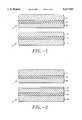
- FIG. 1is a simplified cross sectional view of two silicon wafers.
- FIG. 2is a cross sectional view of two silicon wafers, the second wafer having a layer of titanium deposited according to the present invention.
- FIG. 3is a cross sectional view of the two silicon wafers being bonded in a furnace being exposed to an inert ambience.
- FIG. 4is a cross sectional view of two silicon wafers having a layer of titanium deposited according to an alternative embodiment of the present invention.
- FIG. 5is a cross sectional view of the two silicon wafers being bonded in a furnace being exposed to an inert ambience according to an alternative embodiment of the present invention.
- FIG. 6is a cross sectional view of a first wafer having a silicon layer deposited and a second wafer having titanium deposited according to an alternative embodiment of the present invention.
- FIG. 7is a cross sectional view of the two silicon wafers being bonded in a furnace being exposed to an inert ambience according to an alternative embodiment of the present invention.
- FIG. 8is a flow diagram of aluminum to aluminum bonding according to the present invention.
- FIG. 9is a flow diagram of aluminum to aluminum bonding according to an alternative embodiment of the present invention.
- FIG. 10is a flow diagram of bonding aluminum alloys according to an alternative embodiment of the present invention.
- FIG. 11shows a multichip module (MCM) having multiple modules interconnected with top level metals.
- MCMmultichip module
- FIG. 1shows simplified layering of two silicon wafers 1 and 2.
- the silicon wafers 1 and 2contain integrated circuits that have been formed using processes well known in the art.
- Wafer 1includes a silicon (Si) layer 4, a silicon oxide layer 6, and an aluminum (Al) layer 8. Many devices are formed on the silicon layer 4.
- the silicon oxide layer 6provides insulation between the devices formed on the silicon layer 4 and the aluminum layer 8.
- the aluminum layer 8is a metal layer that provides interconnections for the devices formed on the silicon layer 4.
- Wafer 2is similar to wafer 1.
- Wafer 2includes a silicon layer 14, a silicon oxide layer 12, and an aluminum layer 10. Many devices are formed on the silicon layer 14.
- the silicon oxide layer 12provides insulation between the devices formed on the silicon layer 14 and the aluminum layer 10.
- the aluminum layer 10is a metal layer that provides interconnections for the devices formed on the silicon layer 14.
- Tititanium
- Metallization of the titanium layer 16 onto the aluminum 10 of wafer 2is well known in the art.
- One technique to perform the metallizationis to use a process known as physical vapor deposition (PVD).
- PVDphysical vapor deposition
- Other deposition processescan also be used.
- the processesinclude deposition of films by thermal evaporation and sputter deposition. Approximately 250 angstroms of titanium are deposited onto the aluminum layer 10. Prior to deposition, care is taken to remove aluminum oxide that may have formed on the aluminum surface. Additionally, after deposition of the titanium, care is taken to prevent oxidation of the titanium. Any exposure of the titanium to air can cause oxidation.
- the aluminum layer 8 of wafer 1 and the titanium layer 16 of wafer 2are brought in physical contact and pressed together to maintain the physical contact between the wafers.
- the wafers 1 and 2are placed in a furnace 15 and furnace annealed at a temperature in the range of approximately 400° C. to 550° C. for 15-20 minutes in an inert ambience. Care is taken to evacuate any oxygen from the inert ambiance of the furnace 15.
- the inert ambiancemay be Nitrogen or Argon, for example.
- the titanium layer 16reacts with the aluminum layers 8 and 10 to form the TiAl 3 intermetallic compound between the aluminum layers.
- the Ti--Al bondsprovides the intermetallic compound having a resistivity of approximately 30 ⁇ -cm.
- the intermetallic compound Ti--Alaffords a low resistivity path for the interconnects between the integrated circuits of wafer 1 and wafer 2.
- top layer metallization metalsmay be used.
- a layer of titaniumis deposited to the copper for bonding copper top layers of wafers together.
- the titanium top layerscan also be bonded to provide the low resistive bonds.
- electrically conductive connections between wafer 1 and wafer 2are formed. These electrically conductive connections provide low resistive IC level interconnects that allow peak circuit from the interconnected devices of wafer 1 and wafer 2.
- FIG. 4shows that wafer 3 is also deposited with a titanium layer 18.
- the deposited titanium layer 18is approximately 250 angstroms.
- wafer 3includes the silicon (Si) layer 4, the silicon oxide layer 6, and the aluminum (Al) layer 8. Many devices are formed on the silicon layer 4.
- the silicon oxide layer 6provides insulation between the devices formed on the silicon layer 4 and the aluminum layer 8.
- the aluminum layer 8is the metal layer that provides interconnections for the devices formed on the silicon layer 4.
- Wafer 5 similar to the wafer 2 of FIG. 2includes the titanium layer 16, the silicon layer 14, the silicon oxide layer 12, and the aluminum layer 10. Many devices are formed on the silicon layer 14.
- the silicon oxide layer 12provides insulation between the devices formed on the silicon layer 14 and the aluminum layer 10.
- the aluminum layer 10is the metal layer that provides interconnections for the integrated circuits formed on the silicon layer 4.
- the titanium layer 18 of wafer 3 and the titanium layer 16 of wafer 5are brought in physical contact and pressed together.
- the wafers 3 and 5are placed in the furnace 15 and furnace annealed at a temperature in the range of approximately 400° C. to 550° C. for 15-20 minutes in an inert ambience in the absence of oxygen.
- the inert ambiancemay be Nitrogen or Argon, for example.
- the titanium layer 16 and titanium layer 18react with the aluminum layers 8 and 10 to form Ti--Al bonds between the aluminum layers.
- the Ti--Al bondsprovides an intermetallic compound having a resistivity of approximately 30 ⁇ -cm.
- the intermetallic compound Ti--Alaffords a low resistivity path for the interconnects between the integrated circuits of wafer 3 and wafer 5.
- electrically conductive connections between wafer 3 and wafer 5are formed. These electrically conductive connections provide low resistive IC level interconnects that allow peak circuit speed from the interconnected devices of wafer 3 and wafer 5.
- FIG. 6shows a wafer 7 having approximately 400 angstroms of a silicon layer 20 deposited onto the aluminum layer 8.
- Wafer 9has approximately 500 angstroms of a titanium 16 deposited onto the aluminum.
- wafer 7includes the silicon (Si) layer 4, the silicon oxide layer 6, and the aluminum (Al) layer 8. Many devices are formed on the silicon layer 4.
- the silicon oxide layer 6provides insulation between the devices formed on the silicon layer 4 and the aluminum layer 8.
- the aluminum layer 8is the metal layer that provides interconnections for the devices formed on the silicon layer 4.
- Wafer 9being similar to wafer 7 also includes the silicon layer 14, the silicon oxide layer 12, and the aluminum layer 10. Many devices are formed on the silicon layer 14.
- the silicon oxide layer 12provides insulation between devices formed on the silicon layer 14 and the aluminum layer 10.
- the aluminum layer 10provides interconnections for the integrated circuits formed on the silicon layer 4.
- the silicon layer 20 of wafer 7 and the titanium layer 16 of wafer 9are brought in physical contact and pressed together.
- a higher annealing budgetis provided.
- the wafers 7 and 9are placed in the furnace 15 and furnace annealed at a temperature of approximately 500° C. for approximately 30 minutes in an inert ambience in the absence of oxygen.
- the inert ambiancemay be Nitrogen or Argon, for example.
- the titanium layer 16reacts with the aluminum layers 8 and 10 to form Ti--Al and Ti--Si bonds between the aluminum layers.
- Ti--Al and the Ti--Si bondsprovide intermetallic compounds (TiAl 3 , Ti x Si y , TiAl a Si b ) having low resistivity that affords a low resistivity path for the interconnects between the integrated circuits of wafer 7 and wafer 9.
- electrically conductive connections between wafer 7 and wafer 9are formed. These electrically conductive connections provide low resistive IC level interconnects that allow peak circuit speed from the interconnected devices of wafer 7 and wafer 9.
- FIG. 8shows a flow diagram for bonding aluminum to achieve a low resistive bond according to the present invention.
- the flow diagrambegins with step 81.
- Step 82deposits 250 angstroms of titanium onto the aluminum layer of wafer 2.
- step 84places the aluminum layer of wafer 1 and the titanium layer of wafer 2 in physical contact.
- wafer 1 and wafer 2are furnace annealed at approximately 400° C. to 550° C. in an inert ambience for approximately 15 to 20 minutes as needed to form the low resistive bond.
- the low resistive bondprovides an electrically conductive bond between wafer 1 and wafer 2.
- the flow diagramis complete at finish step 87.
- FIG. 9shows a flow diagram of an alternative embodiment for bonding aluminum to achieve a low resistive bond according to the present invention.
- the flow diagrambegins with step 91.
- Step 92deposits 250 angstroms of titanium onto the aluminum layer of wafer 3.
- Step 94deposits 250 angstroms of titanium onto the aluminum layer of wafer 5.
- step 96places the titanium layer of wafer 3 and the titanium layer of wafer 5 in physical contact.
- step 98wafer 3 and wafer 5 are furnace annealed at approximately 400° C. to 550° C. in an inert ambience for approximately 15 to 20 minutes to form the low resistive bond.
- the low resistive bondprovides an electrically conductive bond between wafer 3 and wafer 5.
- the flow diagramis complete at finish step 99.
- FIG. 10shows a flow diagram of another alternative embodiment for bonding aluminum alloys to achieve a low resistive bond according to the present invention.
- the flow diagrambegins with step 101.
- Step 102deposits 400 angstroms of silicon onto the aluminum layer of wafer 7.
- Step 104deposits 500 angstroms of titanium onto the aluminum layer of wafer 9.
- step 106places the silicon layer of wafer 7 and the titanium layer of wafer 9 in physical contact.
- step 108wafer 7 and wafer 9 are furnace annealed at approximately 500° C. in an inert ambience for approximately 30 minutes to form the low resistive bond.
- the low resistive bondprovides an electrically conductive bond between wafer 7 and wafer 9.
- the flow diagramis complete at finish step 109.
- FIG. 11shows a multichip module (MCM) having multiple modules interconnected with top level metals.
- MGM 110includes integrated circuit (IC) modules 112, 114, 116, and 118 and a common substrate base 111.
- the common substrate base 111provides interconnects for the modules 112, 114, 116, and 118.
- the IC modules 112, 114, 116, and 118 and the common substrate base 111are interconnected to provide functionality to MCM 110. For simplicity, additional wirebond or TAB connections, external pins are not shown.
- the IC modules 112, 116, and 118are coupled to the common substrate base 111. Die bond adhesives well known in the art is used to attach the IC modules 112, 116, and 118 to the substrate.
- the top level metal of the IC modules 112, 116, and 118are coupled to the top level metal of module 114.
- the IC module 114is flipped to allow the top level metal to couple with the top level metals of the IC modules 112, 116, and 118.
- a direct IC module connection between IC modules 114 and 112, 114 and 118, and 114 and 116is achieved.
- Other variations of direct IC module connectionsare achievable depending on the system design.
- IC module designs optimized for direct IC module connectionswill rely more on interconnects using direct connection and rely less on interconnects between IC modules using wirebond and tape automated bonding (TAB) techniques for circuits which perform at higher circuit speeds.
- TABwirebond and tape automated bonding
- the interconnects between multichip modulesare directly bonded reducing interconnections through the use of interconnection substrates, wirebonds, and TAB techniques.
- Direct connections between top level metalsoffer stronger connections and shorter paths between the IC modules.
- the shorter paths between the IC modulesreduce crosstalk between interconnects during high frequency operations.
- the overall system speed and performance of an MCMis increased.
- top level metal bonds between IC modulesaffords three dimensional configuration of IC modules.
- the stacking of the IC modules in the three dimensional configurationalso reduces the overall footprint of the MCMs to provide more compactness.
Landscapes
- Engineering & Computer Science (AREA)
- Microelectronics & Electronic Packaging (AREA)
- Computer Hardware Design (AREA)
- Power Engineering (AREA)
- Manufacturing & Machinery (AREA)
- Physics & Mathematics (AREA)
- Condensed Matter Physics & Semiconductors (AREA)
- General Physics & Mathematics (AREA)
- Internal Circuitry In Semiconductor Integrated Circuit Devices (AREA)
Abstract
Description
1. Field of the Invention
The present invention relates to interconnecting multichip modules and more particularly to forming electrically conductive metal bonds between integrated circuit devices.
2. Description of Previous Art
As advances in processing technology allow ever increasing number of integrated components to be fabricated on an integrated circuit (IC), The industry is constantly striving to integrate more circuit devices for each packaged integrated circuit.
Often times, the speed at which a system can operate is limited by resistor-capacitor (RC) delay and crosstalk coupling of one signal into another. The RC delay and crosstalk coupling problems are even more prominent as IC devices becomes smaller.
One technique that allows more circuit devices and more performance from a packaged IC is through the use of multichip modules (MCMs) technology. MCMs integrates a plurality of individual modules of circuit devices formed on a single IC die. MCMs have the advantage of increasing yields of highly complex ICs by piecing a complex IC together with smaller IC components. In this way, defects that do occur effect individual components of the MCM rather than a single large complex die. Defects affecting the larger dies are much more costly.
The IC modules of the MCM packages are bare ICs. Many of these ICs are fabricated on top of a monolithic silicon IC wafer and designed for perimeter wire bonding. Devices are first formed on the silicon IC wafer. Multiple metallization layers are formed on the bare IC to provide a connection medium from the IC to the outside world and within the IC. Aluminum is commonly used for the metallization layers because aluminum exhibits desirable properties such as ease of processing and low resistivity. The top most level metal is deposited and patterned during the last stages of processing, whereas the gates, contacts, and the metallization of the devices are formed during earlier stages. The top level metal is thick because it is a current carrier for the IC.
Many MCM designs have evolved and is continuing to develop. A basic MCM design has a structure having two or more IC modules electrically connected to an interconnect substrate. The interconnect substrate has patterns formed on multiple layers to provide the interconnects to the IC modules. The multiple layers are separated by dielectric to prevent shorting between the layers. Contacts formed on the IC modules and the interconnect substrate provide coupling points for first level connections which couple the IC modules to the interconnect substrate. Additional contacts formed on the interconnect substrate provide second level connection points which couple the interconnect substrate to external pins of the packaged MCM.
MCMs have fundamental advantages of increased speed, reduced number of external connections, and reduced overall size. The interconnects between the IC modules are substantially shorter than what would otherwise be traces on a printed circuit board. The short interconnects increase signal integrity and reduce crosstalk. The number of external connections to the packaged IC is also reduced. Signals between the IC modules of the MCM are interconnected within the MCM. Furthermore, the overall size of an MCM is reduced by integrating many IC modules into a single MCM package.
In order to achieve peak performance from a system of individual ICs, it is desirable to keep connections between the individual ICs as short a possible. Circuit speed on the bare IC level is the highest speed achievable for the IC. As soon as interconnects are introduced, circuit speed begins to suffer. In an MCM, it is advantageous to limit interconnects lengths between the ICs.
Wirebond and tape automated bonding (TAB) techniques are used to provide connections between the IC modules and the MCM substrate. These techniques use leads for carrying electrical signals from one IC module to another. Thus, wirebond and TAB techniques suffer from circuit speed degradation and crosstalk that are inherent in lead designs. Some MCM designs have addressed reduced interconnect lead problems by using a flip chip solder bump (FCSB) technology.
IBM first introduced the FCSB interconnections in 1964. FCSB interconnections are still widely practiced by IBM today. Bare ICs with solder bump terminals and a matching set of solder pads on a substrate are mated to produce interconnections between the ICs of the MCM. The ICs are placed upside down or flipped to mate with the substrate. In this way, interconnects between the IC modules are kept at a minimum. Solder bumps are used to attach the IC modules and the substrate. Each solder bump is aligned with it matching substrate pad. All the solder joints are processed simultaneously by reflowing the solder in a furnace.
There are however some disadvantages of the FCSB interconnections. The disadvantages arise from the connection medium between the flipped ICs and the underlying MCM substrate. The MCM substrate is typically much larger than the ICs. Multiple ICs are attached to the MCM substrate to form the MCM. The larger MCM substrates are more complex to build which reduces the yield of FCSB MCMs. Furthermore, because the MCM substrate functions to interconnect the IC modules, parasitic capacitance present in the larger and more complex substrate degrades electrical performance of the IC modules. Thus, FCSB interconnections adds cost and complexity to the fabrication of MCM modules.
Therefore, it is desirable to provide interconnects well suited for IC modules, and a method of operating the same which preserve bare IC circuit speed and performance without suffering from disadvantages of previous MCM designs.
The various objects of the invention which are presented and which will become apparent below are provided by example only and are not intended to limit the scope of the present invention. The present invention is to be limited in scope only by the appended claims.
It is an object of the present invention to bond top level metals of devices formed on a silicon substrate.
It is a further object to provide low resistive bonds between aluminum.
It is a further object to bond aluminum with aluminum in temperatures below the melting point of aluminum.
It is a further object to provide interconnects well suited IC modules.
It is a further object to reduce fanout of IC modules contained in MCMs.
It is a further object to provide three dimensional multichip structures.
It is a further object to provide MCMs that exhibit greater circuit speed.
In accordance with the above objects and those that will be mentioned and will become apparent below, a method for bonding flat metal surfaces comprising the steps of:
depositing a thin layer of titanium on a first surface of a first metal surface;
placing the first surface of the first metal surface in contact with a first surface of a second metal surface in an inert ambiance;
heating the inert ambiance to a temperature substantially below the melting point of the metal surfaces; and
forming a titanium metal bond between the first metal surface and the second metal surface to provide a low resistive path between the first metal surface and the second metal surface.
According to one aspect of the invention, the method further comprises depositing a thin layer of titanium on the first surface of the second metal surface. The first flat metal surface and the second flat metal surface are top level metal surfaces of bare ICs which are formed with aluminum. Thus, a metal bond of TiAl3 is formed between the metal surfaces. Aluminum exhibits desirable properties for use as a top level metal because of its ease of processing and low resistivity The top level metal of a bare IC provides a connection medium from the IC to the outside world and is deposited and patterned during the last stages of processing. As the top level metal, it is a current carrier and is therefore thick.
According to another aspect of the invention, the inert ambiance includes nitrogen and argon which is heated in a furnace to a temperature between 400° C. and 550° C. The first flat metal surface and the second flat metal surface are heated for about 15 to 20 minutes.
According to yet another aspect of the invention, the thin layer of titanium is approximately 250 angstroms.
A method of bonding a first metal surface and a second metal surface is provided which exhibits low resistivity. The method of bonding is performed at low processing temperatures in an inert ambiance. The method of bonding is applicable to aluminum and other conductive metals which are widely used for top level metals of bare ICs fabricated on silicon substrates. Thus, by bonding top level metals of bare ICs to form interconnects between the bare ICs, three dimensional MCMs that have smaller fanouts and offering greater circuit speed performance are realizable.
It is an advantage of the present invention to provide bonding of top level metals of devices formed on a silicon substrate.
It is a further advantage to provide low resistive bonds between aluminum.
It is a further advantage to bond aluminum with aluminum in temperatures below the melting point of aluminum.
It is a further advantage to provide interconnects well suited IC modules.
It is a further advantage to reduce fanout of IC modules contained in MCMs.
It is a further advantage to provide three dimensional multichip structures.
It is a further advantage to provide MCMs that exhibit greater circuit speed.
FIG. 1 is a simplified cross sectional view of two silicon wafers.
FIG. 2 is a cross sectional view of two silicon wafers, the second wafer having a layer of titanium deposited according to the present invention.
FIG. 3 is a cross sectional view of the two silicon wafers being bonded in a furnace being exposed to an inert ambiance.
FIG. 4 is a cross sectional view of two silicon wafers having a layer of titanium deposited according to an alternative embodiment of the present invention.
FIG. 5 is a cross sectional view of the two silicon wafers being bonded in a furnace being exposed to an inert ambiance according to an alternative embodiment of the present invention.
FIG. 6 is a cross sectional view of a first wafer having a silicon layer deposited and a second wafer having titanium deposited according to an alternative embodiment of the present invention.
FIG. 7 is a cross sectional view of the two silicon wafers being bonded in a furnace being exposed to an inert ambiance according to an alternative embodiment of the present invention.
FIG. 8 is a flow diagram of aluminum to aluminum bonding according to the present invention.
FIG. 9 is a flow diagram of aluminum to aluminum bonding according to an alternative embodiment of the present invention.
FIG. 10 is a flow diagram of bonding aluminum alloys according to an alternative embodiment of the present invention.
FIG. 11 shows a multichip module (MCM) having multiple modules interconnected with top level metals.
A detailed description of preferred embodiments of the present invention is provided with respect to the drawings. Like characters refer to like elements throughout. FIG. 1 shows simplified layering of twosilicon wafers silicon wafers Wafer 1 includes a silicon (Si)layer 4, asilicon oxide layer 6, and an aluminum (Al)layer 8. Many devices are formed on thesilicon layer 4. Thesilicon oxide layer 6 provides insulation between the devices formed on thesilicon layer 4 and thealuminum layer 8. Thealuminum layer 8 is a metal layer that provides interconnections for the devices formed on thesilicon layer 4.
With respect to FIG. 2, there is shown a titanium (Ti)layer 16 that is formed on thealuminum layer 10 ofwafer 2. Metallization of thetitanium layer 16 onto thealuminum 10 ofwafer 2 is well known in the art. One technique to perform the metallization is to use a process known as physical vapor deposition (PVD). Other deposition processes can also be used. The processes include deposition of films by thermal evaporation and sputter deposition. Approximately 250 angstroms of titanium are deposited onto thealuminum layer 10. Prior to deposition, care is taken to remove aluminum oxide that may have formed on the aluminum surface. Additionally, after deposition of the titanium, care is taken to prevent oxidation of the titanium. Any exposure of the titanium to air can cause oxidation.
Referring to FIG. 3, thealuminum layer 8 ofwafer 1 and thetitanium layer 16 ofwafer 2 are brought in physical contact and pressed together to maintain the physical contact between the wafers. Thewafers furnace 15 and furnace annealed at a temperature in the range of approximately 400° C. to 550° C. for 15-20 minutes in an inert ambiance. Care is taken to evacuate any oxygen from the inert ambiance of thefurnace 15. The inert ambiance may be Nitrogen or Argon, for example. During the annealing process, thetitanium layer 16 reacts with the aluminum layers 8 and 10 to form the TiAl3 intermetallic compound between the aluminum layers. The Ti--Al bonds provides the intermetallic compound having a resistivity of approximately 30 μΩ-cm. The intermetallic compound Ti--Al affords a low resistivity path for the interconnects between the integrated circuits ofwafer 1 andwafer 2.
Although Aluminum is presented throughout as the top layer of the wafers in the various embodiments, other top layer metallization metals may be used. For example, if copper is used as the top layer of wafers, a layer of titanium is deposited to the copper for bonding copper top layers of wafers together. If titanium is used as the top layer of wafers, the titanium top layers can also be bonded to provide the low resistive bonds.
By properly patterning thealuminum layer wafer 1 andwafer 2 are formed. These electrically conductive connections provide low resistive IC level interconnects that allow peak circuit from the interconnected devices ofwafer 1 andwafer 2.
In a second embodiment, FIG. 4 shows thatwafer 3 is also deposited with atitanium layer 18. The depositedtitanium layer 18 is approximately 250 angstroms. Similar deposition techniques used for the deposition of thetitanium layer 16 ofwafer 4 in FIG. 2 can also be applied towafer 3. Thus,wafer 3 includes the silicon (Si)layer 4, thesilicon oxide layer 6, and the aluminum (Al)layer 8. Many devices are formed on thesilicon layer 4. Thesilicon oxide layer 6 provides insulation between the devices formed on thesilicon layer 4 and thealuminum layer 8. Thealuminum layer 8 is the metal layer that provides interconnections for the devices formed on thesilicon layer 4.Wafer 5 similar to thewafer 2 of FIG. 2 includes thetitanium layer 16, thesilicon layer 14, thesilicon oxide layer 12, and thealuminum layer 10. Many devices are formed on thesilicon layer 14. Thesilicon oxide layer 12 provides insulation between the devices formed on thesilicon layer 14 and thealuminum layer 10. Thealuminum layer 10 is the metal layer that provides interconnections for the integrated circuits formed on thesilicon layer 4.
With respect to FIG. 5, there is shown that thetitanium layer 18 ofwafer 3 and thetitanium layer 16 ofwafer 5 are brought in physical contact and pressed together. Thewafers furnace 15 and furnace annealed at a temperature in the range of approximately 400° C. to 550° C. for 15-20 minutes in an inert ambiance in the absence of oxygen. The inert ambiance may be Nitrogen or Argon, for example. During the annealing process, thetitanium layer 16 andtitanium layer 18 react with the aluminum layers 8 and 10 to form Ti--Al bonds between the aluminum layers. The Ti--Al bonds provides an intermetallic compound having a resistivity of approximately 30 μΩ-cm. The intermetallic compound Ti--Al affords a low resistivity path for the interconnects between the integrated circuits ofwafer 3 andwafer 5.
By properly patterning thealuminum layer wafer 3 andwafer 5 are formed. These electrically conductive connections provide low resistive IC level interconnects that allow peak circuit speed from the interconnected devices ofwafer 3 andwafer 5.
In another embodiment, aluminum alloys are used to form a low resistive bond betweenwafer 7 andwafer 9. FIG. 6 shows awafer 7 having approximately 400 angstroms of asilicon layer 20 deposited onto thealuminum layer 8.Wafer 9 has approximately 500 angstroms of atitanium 16 deposited onto the aluminum. Thus,wafer 7 includes the silicon (Si)layer 4, thesilicon oxide layer 6, and the aluminum (Al)layer 8. Many devices are formed on thesilicon layer 4. Thesilicon oxide layer 6 provides insulation between the devices formed on thesilicon layer 4 and thealuminum layer 8. Thealuminum layer 8 is the metal layer that provides interconnections for the devices formed on thesilicon layer 4.Wafer 9 being similar towafer 7 also includes thesilicon layer 14, thesilicon oxide layer 12, and thealuminum layer 10. Many devices are formed on thesilicon layer 14. Thesilicon oxide layer 12 provides insulation between devices formed on thesilicon layer 14 and thealuminum layer 10. Thealuminum layer 10 provides interconnections for the integrated circuits formed on thesilicon layer 4.
With respect to FIG. 7, there is shown that thesilicon layer 20 ofwafer 7 and thetitanium layer 16 ofwafer 9 are brought in physical contact and pressed together. In order to form a low resistive bond, a higher annealing budget is provided. Thewafers furnace 15 and furnace annealed at a temperature of approximately 500° C. for approximately 30 minutes in an inert ambiance in the absence of oxygen. The inert ambiance may be Nitrogen or Argon, for example. During the annealing process, thetitanium layer 16 reacts with the aluminum layers 8 and 10 to form Ti--Al and Ti--Si bonds between the aluminum layers. The Ti--Al and the Ti--Si bonds provide intermetallic compounds (TiAl3, Tix Siy, TiAla Sib) having low resistivity that affords a low resistivity path for the interconnects between the integrated circuits ofwafer 7 andwafer 9.
By properly patterning thealuminum layer wafer 7 andwafer 9 are formed. These electrically conductive connections provide low resistive IC level interconnects that allow peak circuit speed from the interconnected devices ofwafer 7 andwafer 9.
FIG. 8 shows a flow diagram for bonding aluminum to achieve a low resistive bond according to the present invention. The flow diagram begins withstep 81.Step 82deposits 250 angstroms of titanium onto the aluminum layer ofwafer 2. Next, step 84 places the aluminum layer ofwafer 1 and the titanium layer ofwafer 2 in physical contact. Instep 86,wafer 1 andwafer 2 are furnace annealed at approximately 400° C. to 550° C. in an inert ambiance for approximately 15 to 20 minutes as needed to form the low resistive bond. The low resistive bond provides an electrically conductive bond betweenwafer 1 andwafer 2. The flow diagram is complete atfinish step 87.
FIG. 9 shows a flow diagram of an alternative embodiment for bonding aluminum to achieve a low resistive bond according to the present invention. The flow diagram begins withstep 91.Step 92deposits 250 angstroms of titanium onto the aluminum layer ofwafer 3.Step 94deposits 250 angstroms of titanium onto the aluminum layer ofwafer 5. Next, step 96 places the titanium layer ofwafer 3 and the titanium layer ofwafer 5 in physical contact. Instep 98,wafer 3 andwafer 5 are furnace annealed at approximately 400° C. to 550° C. in an inert ambiance for approximately 15 to 20 minutes to form the low resistive bond. The low resistive bond provides an electrically conductive bond betweenwafer 3 andwafer 5. The flow diagram is complete at finish step 99.
FIG. 10 shows a flow diagram of another alternative embodiment for bonding aluminum alloys to achieve a low resistive bond according to the present invention. The flow diagram begins withstep 101. Step 102deposits 400 angstroms of silicon onto the aluminum layer ofwafer 7. Step 104deposits 500 angstroms of titanium onto the aluminum layer ofwafer 9. Next, step 106 places the silicon layer ofwafer 7 and the titanium layer ofwafer 9 in physical contact. Instep 108,wafer 7 andwafer 9 are furnace annealed at approximately 500° C. in an inert ambiance for approximately 30 minutes to form the low resistive bond. The low resistive bond provides an electrically conductive bond betweenwafer 7 andwafer 9. The flow diagram is complete atfinish step 109.
FIG. 11 shows a multichip module (MCM) having multiple modules interconnected with top level metals.MGM 110 includes integrated circuit (IC)modules common substrate base 111. Thecommon substrate base 111 provides interconnects for themodules IC modules common substrate base 111 are interconnected to provide functionality toMCM 110. For simplicity, additional wirebond or TAB connections, external pins are not shown. TheIC modules common substrate base 111. Die bond adhesives well known in the art is used to attach theIC modules IC modules module 114. Thus, theIC module 114 is flipped to allow the top level metal to couple with the top level metals of theIC modules IC modules
By creating low resistive Al--Al bonds for electrically conductive bonds, the interconnects between multichip modules are directly bonded reducing interconnections through the use of interconnection substrates, wirebonds, and TAB techniques. Direct connections between top level metals offer stronger connections and shorter paths between the IC modules. The shorter paths between the IC modules reduce crosstalk between interconnects during high frequency operations. Thus, the overall system speed and performance of an MCM is increased.
Additionally, forming top level metal bonds between IC modules affords three dimensional configuration of IC modules. The stacking of the IC modules in the three dimensional configuration also reduces the overall footprint of the MCMs to provide more compactness.
The foregoing description of the preferred embodiments of the invention has been presented for purpose of illustration and description. It is not intended to be exhaustive or to limit the invention to the precise forms disclosed. Obviously, many modifications and variations will be apparent to the practitioners skilled in this art. It is intended that the scope of the invention be defined by the following claims and their equivalents.
Claims (22)
1. A method for bonding flat metal surfaces comprising the steps of:
depositing a thin layer of titanium on a first surface of a first metal surface;
placing the first surface of the first metal surface in contact with a first surface of a second metal surface in an inert ambiance;
heating the inert ambiance to a temperature substantially below the melting point of the metal surfaces; and
forming a titanium metal bond between the first metal surface and the second metal surface to provide a low resistive path between the first metal surface and the second metal surface.
2. The method according to claim 1 further comprising depositing a thin layer of titanium on the first surface of the second metal surface.
3. The method according to claim 1, wherein the first flat metal surface and the second flat metal surface includes aluminum.
4. The method according to claim 1, wherein the first flat metal surface and the second flat metal surface includes copper.
5. The method according to claim 1, wherein the inert ambiance includes nitrogen and argon.
6. The method according to claim 1, wherein the step of heating the inert ambiance includes the step of heating the inert ambiance to a temperature between 400° C. and 550° C.
7. The method according to claim 1, wherein the thin layer of titanium is approximately 250 angstroms.
8. A method of bonding aluminum surfaces comprising the steps of:
depositing a thin layer of titanium on a first surface of a first aluminum surface;
depositing a thin layer of silicon on a first surface of a second aluminum surface;
placing the first surface of the first aluminum surface in contact with the first surface of the second aluminum surface in an inert ambiance;
heating the inert ambiance to a temperature substantially below the melting point of the aluminum surfaces; and
forming a metal bond between the first aluminum surface and the second aluminum surface to provide a low resistive path between the first aluminum surface and the second aluminum surface.
9. The method of bonding according to claim 8, wherein the thin layer of titanium is approximately 500 angstroms.
10. The method of bonding according to claim 8, wherein the thin layer silicon is approximately 400 angstroms.
11. The method of bonding according to claim 8, wherein the inert ambiance includes nitrogen and argon.
12. The method of bonding according to claim 8, wherein the step of heating the inert ambiance includes the step of heating the inert ambiance to a temperature between 400° C. and 550° C.
13. The method of bonding according to claim 8, wherein the step of forming a metal bond includes titanium-aluminum bonds and titanium-silicon bonds.
14. A method of bonding aluminum surfaces comprising the steps of:
depositing a thin layer of titanium on a first surface of a first aluminum surface;
depositing a thin layer of titanium on a first surface of a second aluminum surface;
placing the first surface of the first aluminum surface in contact with the first surface of the second aluminum surface in an inert ambiance;
heating the inert ambiance to a temperature substantially below the melting point of the aluminum surfaces; and
forming a titanium-aluminum bond between the first aluminum surface and the second aluminum surface to provide a low resistive path between the first aluminum surface and the second aluminum surface.
15. A method of interconnecting multichip modules comprising the steps of:
depositing a thin layer of titanium on a first top level metal of a first module;
placing a second top level metal of a second module in contact with the first top level metal of the first module in an inert ambiance;
heating the inert ambiance to a temperature substantially below the melting point of the first top level metal and the second top level metal; and
forming a titanium metal bond between the first top level metal of the first module and the second top level metal of the second module to provide a low resistive path between the first top level metal and the second top level metal.
16. The method of interconnecting according to claim 15, wherein:
the first top level metal includes patterns to provide connections to integrated circuits formed on the first module; and
the second top level metal includes patterns to provide connections to integrated circuits formed on the second module.
17. The method of interconnecting according to claim 15, wherein the step of placing further comprises the step of flipping the second module to contact the second top level metal with the first top level metal of the first module.
18. The method of interconnecting according to claim 15, wherein the first top metal and the second metal are aluminum.
19. The method of interconnecting according to claim 18 further comprising depositing a thin layer of titanium on the second top level metal of the second module.
20. The method of interconnecting according to claim 19, wherein the thin layer of titanium deposited on the first top level metal and the second top level is approximately 250 angstroms.
21. The method of interconnecting according to claim 15, wherein the inert ambiance includes nitrogen and argon.
22. The method of interconnecting according to claim 15, wherein the step of heating the inert ambiance includes the step of heating the inert ambiance to a temperature between 400° C. and 550° C.
Priority Applications (1)
| Application Number | Priority Date | Filing Date | Title |
|---|---|---|---|
| US08/566,070US5617991A (en) | 1995-12-01 | 1995-12-01 | Method for electrically conductive metal-to-metal bonding |
Applications Claiming Priority (1)
| Application Number | Priority Date | Filing Date | Title |
|---|---|---|---|
| US08/566,070US5617991A (en) | 1995-12-01 | 1995-12-01 | Method for electrically conductive metal-to-metal bonding |
Publications (1)
| Publication Number | Publication Date |
|---|---|
| US5617991Atrue US5617991A (en) | 1997-04-08 |
Family
ID=24261351
Family Applications (1)
| Application Number | Title | Priority Date | Filing Date |
|---|---|---|---|
| US08/566,070Expired - LifetimeUS5617991A (en) | 1995-12-01 | 1995-12-01 | Method for electrically conductive metal-to-metal bonding |
Country Status (1)
| Country | Link |
|---|---|
| US (1) | US5617991A (en) |
Cited By (230)
| Publication number | Priority date | Publication date | Assignee | Title |
|---|---|---|---|---|
| US5831252A (en)* | 1995-02-08 | 1998-11-03 | Daido Tokushuko Kabushiki Kaisha | Methods of bonding titanium and titanium alloy members by high frequency heating |
| US5880010A (en)* | 1994-07-12 | 1999-03-09 | Sun Microsystems, Inc. | Ultrathin electronics |
| US20050280042A1 (en)* | 2004-06-21 | 2005-12-22 | Sang-Yun Lee | Wafer bonding method |
| US20050280154A1 (en)* | 2004-06-21 | 2005-12-22 | Sang-Yun Lee | Semiconductor memory device |
| US20050280155A1 (en)* | 2004-06-21 | 2005-12-22 | Sang-Yun Lee | Semiconductor bonding and layer transfer method |
| US20090267233A1 (en)* | 1996-11-04 | 2009-10-29 | Sang-Yun Lee | Bonded semiconductor structure and method of making the same |
| US20100133695A1 (en)* | 2003-01-12 | 2010-06-03 | Sang-Yun Lee | Electronic circuit with embedded memory |
| US20100190334A1 (en)* | 2003-06-24 | 2010-07-29 | Sang-Yun Lee | Three-dimensional semiconductor structure and method of manufacturing the same |
| US20110003438A1 (en)* | 2005-03-29 | 2011-01-06 | Sang-Yun Lee | Three-dimensional integrated circuit structure |
| US20110037497A1 (en)* | 2009-04-14 | 2011-02-17 | Or-Ment Llc | Method for Fabrication of a Semiconductor Device and Structure |
| US20110053332A1 (en)* | 2003-06-24 | 2011-03-03 | Sang-Yun Lee | Semiconductor circuit |
| US20110143506A1 (en)* | 2009-12-10 | 2011-06-16 | Sang-Yun Lee | Method for fabricating a semiconductor memory device |
| US8203148B2 (en) | 2010-10-11 | 2012-06-19 | Monolithic 3D Inc. | Semiconductor device and structure |
| US8237228B2 (en) | 2009-10-12 | 2012-08-07 | Monolithic 3D Inc. | System comprising a semiconductor device and structure |
| US8273610B2 (en) | 2010-11-18 | 2012-09-25 | Monolithic 3D Inc. | Method of constructing a semiconductor device and structure |
| US8294159B2 (en) | 2009-10-12 | 2012-10-23 | Monolithic 3D Inc. | Method for fabrication of a semiconductor device and structure |
| US8362800B2 (en) | 2010-10-13 | 2013-01-29 | Monolithic 3D Inc. | 3D semiconductor device including field repairable logics |
| US8362482B2 (en) | 2009-04-14 | 2013-01-29 | Monolithic 3D Inc. | Semiconductor device and structure |
| US8373230B1 (en) | 2010-10-13 | 2013-02-12 | Monolithic 3D Inc. | Method for fabrication of a semiconductor device and structure |
| US8373439B2 (en) | 2009-04-14 | 2013-02-12 | Monolithic 3D Inc. | 3D semiconductor device |
| US8378494B2 (en) | 2009-04-14 | 2013-02-19 | Monolithic 3D Inc. | Method for fabrication of a semiconductor device and structure |
| US8379458B1 (en) | 2010-10-13 | 2013-02-19 | Monolithic 3D Inc. | Semiconductor device and structure |
| US8378715B2 (en) | 2009-04-14 | 2013-02-19 | Monolithic 3D Inc. | Method to construct systems |
| US8405420B2 (en) | 2009-04-14 | 2013-03-26 | Monolithic 3D Inc. | System comprising a semiconductor device and structure |
| US8427200B2 (en) | 2009-04-14 | 2013-04-23 | Monolithic 3D Inc. | 3D semiconductor device |
| US8440542B2 (en) | 2010-10-11 | 2013-05-14 | Monolithic 3D Inc. | Semiconductor device and structure |
| US8450804B2 (en) | 2011-03-06 | 2013-05-28 | Monolithic 3D Inc. | Semiconductor device and structure for heat removal |
| US8461035B1 (en) | 2010-09-30 | 2013-06-11 | Monolithic 3D Inc. | Method for fabrication of a semiconductor device and structure |
| US8476145B2 (en) | 2010-10-13 | 2013-07-02 | Monolithic 3D Inc. | Method of fabricating a semiconductor device and structure |
| US8492886B2 (en) | 2010-02-16 | 2013-07-23 | Monolithic 3D Inc | 3D integrated circuit with logic |
| US8536023B2 (en) | 2010-11-22 | 2013-09-17 | Monolithic 3D Inc. | Method of manufacturing a semiconductor device and structure |
| US8541819B1 (en) | 2010-12-09 | 2013-09-24 | Monolithic 3D Inc. | Semiconductor device and structure |
| US8557632B1 (en) | 2012-04-09 | 2013-10-15 | Monolithic 3D Inc. | Method for fabrication of a semiconductor device and structure |
| US8574929B1 (en) | 2012-11-16 | 2013-11-05 | Monolithic 3D Inc. | Method to form a 3D semiconductor device and structure |
| US8581349B1 (en) | 2011-05-02 | 2013-11-12 | Monolithic 3D Inc. | 3D memory semiconductor device and structure |
| US8642416B2 (en) | 2010-07-30 | 2014-02-04 | Monolithic 3D Inc. | Method of forming three dimensional integrated circuit devices using layer transfer technique |
| US8669778B1 (en) | 2009-04-14 | 2014-03-11 | Monolithic 3D Inc. | Method for design and manufacturing of a 3D semiconductor device |
| US8674470B1 (en) | 2012-12-22 | 2014-03-18 | Monolithic 3D Inc. | Semiconductor device and structure |
| US8686428B1 (en) | 2012-11-16 | 2014-04-01 | Monolithic 3D Inc. | Semiconductor device and structure |
| US8687399B2 (en) | 2011-10-02 | 2014-04-01 | Monolithic 3D Inc. | Semiconductor device and structure |
| US8709880B2 (en) | 2010-07-30 | 2014-04-29 | Monolithic 3D Inc | Method for fabrication of a semiconductor device and structure |
| US8742476B1 (en) | 2012-11-27 | 2014-06-03 | Monolithic 3D Inc. | Semiconductor device and structure |
| US8753913B2 (en) | 2010-10-13 | 2014-06-17 | Monolithic 3D Inc. | Method for fabricating novel semiconductor and optoelectronic devices |
| US8754533B2 (en) | 2009-04-14 | 2014-06-17 | Monolithic 3D Inc. | Monolithic three-dimensional semiconductor device and structure |
| US8803206B1 (en) | 2012-12-29 | 2014-08-12 | Monolithic 3D Inc. | 3D semiconductor device and structure |
| US8902663B1 (en) | 2013-03-11 | 2014-12-02 | Monolithic 3D Inc. | Method of maintaining a memory state |
| US8901613B2 (en) | 2011-03-06 | 2014-12-02 | Monolithic 3D Inc. | Semiconductor device and structure for heat removal |
| US8975670B2 (en) | 2011-03-06 | 2015-03-10 | Monolithic 3D Inc. | Semiconductor device and structure for heat removal |
| US8994404B1 (en) | 2013-03-12 | 2015-03-31 | Monolithic 3D Inc. | Semiconductor device and structure |
| US9000557B2 (en) | 2012-03-17 | 2015-04-07 | Zvi Or-Bach | Semiconductor device and structure |
| US9012292B2 (en) | 2010-07-02 | 2015-04-21 | Sang-Yun Lee | Semiconductor memory device and method of fabricating the same |
| US9029173B2 (en) | 2011-10-18 | 2015-05-12 | Monolithic 3D Inc. | Method for fabrication of a semiconductor device and structure |
| US9099424B1 (en) | 2012-08-10 | 2015-08-04 | Monolithic 3D Inc. | Semiconductor system, device and structure with heat removal |
| US9099526B2 (en) | 2010-02-16 | 2015-08-04 | Monolithic 3D Inc. | Integrated circuit device and structure |
| US9117749B1 (en) | 2013-03-15 | 2015-08-25 | Monolithic 3D Inc. | Semiconductor device and structure |
| US9197804B1 (en) | 2011-10-14 | 2015-11-24 | Monolithic 3D Inc. | Semiconductor and optoelectronic devices |
| US9219005B2 (en) | 2011-06-28 | 2015-12-22 | Monolithic 3D Inc. | Semiconductor system and device |
| US9509313B2 (en) | 2009-04-14 | 2016-11-29 | Monolithic 3D Inc. | 3D semiconductor device |
| US9577642B2 (en) | 2009-04-14 | 2017-02-21 | Monolithic 3D Inc. | Method to form a 3D semiconductor device |
| US9711407B2 (en) | 2009-04-14 | 2017-07-18 | Monolithic 3D Inc. | Method of manufacturing a three dimensional integrated circuit by transfer of a mono-crystalline layer |
| US9871034B1 (en) | 2012-12-29 | 2018-01-16 | Monolithic 3D Inc. | Semiconductor device and structure |
| US9953925B2 (en) | 2011-06-28 | 2018-04-24 | Monolithic 3D Inc. | Semiconductor system and device |
| US10043781B2 (en) | 2009-10-12 | 2018-08-07 | Monolithic 3D Inc. | 3D semiconductor device and structure |
| US10115663B2 (en) | 2012-12-29 | 2018-10-30 | Monolithic 3D Inc. | 3D semiconductor device and structure |
| US10127344B2 (en) | 2013-04-15 | 2018-11-13 | Monolithic 3D Inc. | Automation for monolithic 3D devices |
| US10157909B2 (en) | 2009-10-12 | 2018-12-18 | Monolithic 3D Inc. | 3D semiconductor device and structure |
| US10217667B2 (en) | 2011-06-28 | 2019-02-26 | Monolithic 3D Inc. | 3D semiconductor device, fabrication method and system |
| US10224279B2 (en) | 2013-03-15 | 2019-03-05 | Monolithic 3D Inc. | Semiconductor device and structure |
| US10290682B2 (en) | 2010-10-11 | 2019-05-14 | Monolithic 3D Inc. | 3D IC semiconductor device and structure with stacked memory |
| US10297586B2 (en) | 2015-03-09 | 2019-05-21 | Monolithic 3D Inc. | Methods for processing a 3D semiconductor device |
| US10325651B2 (en) | 2013-03-11 | 2019-06-18 | Monolithic 3D Inc. | 3D semiconductor device with stacked memory |
| US10354995B2 (en) | 2009-10-12 | 2019-07-16 | Monolithic 3D Inc. | Semiconductor memory device and structure |
| US10366970B2 (en) | 2009-10-12 | 2019-07-30 | Monolithic 3D Inc. | 3D semiconductor device and structure |
| US10381328B2 (en) | 2015-04-19 | 2019-08-13 | Monolithic 3D Inc. | Semiconductor device and structure |
| US10388863B2 (en) | 2009-10-12 | 2019-08-20 | Monolithic 3D Inc. | 3D memory device and structure |
| US10388568B2 (en) | 2011-06-28 | 2019-08-20 | Monolithic 3D Inc. | 3D semiconductor device and system |
| US10418369B2 (en) | 2015-10-24 | 2019-09-17 | Monolithic 3D Inc. | Multi-level semiconductor memory device and structure |
| US10497713B2 (en) | 2010-11-18 | 2019-12-03 | Monolithic 3D Inc. | 3D semiconductor memory device and structure |
| US10515981B2 (en) | 2015-09-21 | 2019-12-24 | Monolithic 3D Inc. | Multilevel semiconductor device and structure with memory |
| US10522225B1 (en) | 2015-10-02 | 2019-12-31 | Monolithic 3D Inc. | Semiconductor device with non-volatile memory |
| US10600888B2 (en) | 2012-04-09 | 2020-03-24 | Monolithic 3D Inc. | 3D semiconductor device |
| US10600657B2 (en) | 2012-12-29 | 2020-03-24 | Monolithic 3D Inc | 3D semiconductor device and structure |
| US10651054B2 (en) | 2012-12-29 | 2020-05-12 | Monolithic 3D Inc. | 3D semiconductor device and structure |
| US10679977B2 (en) | 2010-10-13 | 2020-06-09 | Monolithic 3D Inc. | 3D microdisplay device and structure |
| US10825779B2 (en) | 2015-04-19 | 2020-11-03 | Monolithic 3D Inc. | 3D semiconductor device and structure |
| US10833108B2 (en) | 2010-10-13 | 2020-11-10 | Monolithic 3D Inc. | 3D microdisplay device and structure |
| US10840239B2 (en) | 2014-08-26 | 2020-11-17 | Monolithic 3D Inc. | 3D semiconductor device and structure |
| US10847540B2 (en) | 2015-10-24 | 2020-11-24 | Monolithic 3D Inc. | 3D semiconductor memory device and structure |
| US10892016B1 (en) | 2019-04-08 | 2021-01-12 | Monolithic 3D Inc. | 3D memory semiconductor devices and structures |
| US10892169B2 (en) | 2012-12-29 | 2021-01-12 | Monolithic 3D Inc. | 3D semiconductor device and structure |
| US10896931B1 (en) | 2010-10-11 | 2021-01-19 | Monolithic 3D Inc. | 3D semiconductor device and structure |
| US10903089B1 (en) | 2012-12-29 | 2021-01-26 | Monolithic 3D Inc. | 3D semiconductor device and structure |
| US10910364B2 (en) | 2009-10-12 | 2021-02-02 | Monolitaic 3D Inc. | 3D semiconductor device |
| US10943934B2 (en) | 2010-10-13 | 2021-03-09 | Monolithic 3D Inc. | Multilevel semiconductor device and structure |
| US10978501B1 (en) | 2010-10-13 | 2021-04-13 | Monolithic 3D Inc. | Multilevel semiconductor device and structure with waveguides |
| US10998374B1 (en) | 2010-10-13 | 2021-05-04 | Monolithic 3D Inc. | Multilevel semiconductor device and structure |
| US11004694B1 (en) | 2012-12-29 | 2021-05-11 | Monolithic 3D Inc. | 3D semiconductor device and structure |
| US11004719B1 (en) | 2010-11-18 | 2021-05-11 | Monolithic 3D Inc. | Methods for producing a 3D semiconductor memory device and structure |
| US11011507B1 (en) | 2015-04-19 | 2021-05-18 | Monolithic 3D Inc. | 3D semiconductor device and structure |
| US11018116B2 (en) | 2012-12-22 | 2021-05-25 | Monolithic 3D Inc. | Method to form a 3D semiconductor device and structure |
| US11018191B1 (en) | 2010-10-11 | 2021-05-25 | Monolithic 3D Inc. | 3D semiconductor device and structure |
| US11018133B2 (en) | 2009-10-12 | 2021-05-25 | Monolithic 3D Inc. | 3D integrated circuit |
| US11018042B1 (en) | 2010-11-18 | 2021-05-25 | Monolithic 3D Inc. | 3D semiconductor memory device and structure |
| US11018156B2 (en) | 2019-04-08 | 2021-05-25 | Monolithic 3D Inc. | 3D memory semiconductor devices and structures |
| US11024673B1 (en) | 2010-10-11 | 2021-06-01 | Monolithic 3D Inc. | 3D semiconductor device and structure |
| US11030371B2 (en) | 2013-04-15 | 2021-06-08 | Monolithic 3D Inc. | Automation for monolithic 3D devices |
| US11031394B1 (en) | 2014-01-28 | 2021-06-08 | Monolithic 3D Inc. | 3D semiconductor device and structure |
| US11031275B2 (en) | 2010-11-18 | 2021-06-08 | Monolithic 3D Inc. | 3D semiconductor device and structure with memory |
| US11043523B1 (en) | 2010-10-13 | 2021-06-22 | Monolithic 3D Inc. | Multilevel semiconductor device and structure with image sensors |
| US11056468B1 (en) | 2015-04-19 | 2021-07-06 | Monolithic 3D Inc. | 3D semiconductor device and structure |
| US11063071B1 (en) | 2010-10-13 | 2021-07-13 | Monolithic 3D Inc. | Multilevel semiconductor device and structure with waveguides |
| US11063024B1 (en) | 2012-12-22 | 2021-07-13 | Monlithic 3D Inc. | Method to form a 3D semiconductor device and structure |
| US11088130B2 (en) | 2014-01-28 | 2021-08-10 | Monolithic 3D Inc. | 3D semiconductor device and structure |
| US11088050B2 (en) | 2012-04-09 | 2021-08-10 | Monolithic 3D Inc. | 3D semiconductor device with isolation layers |
| US11087995B1 (en) | 2012-12-29 | 2021-08-10 | Monolithic 3D Inc. | 3D semiconductor device and structure |
| US11094576B1 (en) | 2010-11-18 | 2021-08-17 | Monolithic 3D Inc. | Methods for producing a 3D semiconductor memory device and structure |
| US11107721B2 (en) | 2010-11-18 | 2021-08-31 | Monolithic 3D Inc. | 3D semiconductor device and structure with NAND logic |
| US11107808B1 (en) | 2014-01-28 | 2021-08-31 | Monolithic 3D Inc. | 3D semiconductor device and structure |
| US11114427B2 (en) | 2015-11-07 | 2021-09-07 | Monolithic 3D Inc. | 3D semiconductor processor and memory device and structure |
| US11114464B2 (en) | 2015-10-24 | 2021-09-07 | Monolithic 3D Inc. | 3D semiconductor device and structure |
| US11121021B2 (en) | 2010-11-18 | 2021-09-14 | Monolithic 3D Inc. | 3D semiconductor device and structure |
| US11133344B2 (en) | 2010-10-13 | 2021-09-28 | Monolithic 3D Inc. | Multilevel semiconductor device and structure with image sensors |
| US11158652B1 (en) | 2019-04-08 | 2021-10-26 | Monolithic 3D Inc. | 3D memory semiconductor devices and structures |
| US11158674B2 (en) | 2010-10-11 | 2021-10-26 | Monolithic 3D Inc. | Method to produce a 3D semiconductor device and structure |
| US11163112B2 (en) | 2010-10-13 | 2021-11-02 | Monolithic 3D Inc. | Multilevel semiconductor device and structure with electromagnetic modulators |
| US11164811B2 (en) | 2012-04-09 | 2021-11-02 | Monolithic 3D Inc. | 3D semiconductor device with isolation layers and oxide-to-oxide bonding |
| US11164898B2 (en) | 2010-10-13 | 2021-11-02 | Monolithic 3D Inc. | Multilevel semiconductor device and structure |
| US11164770B1 (en) | 2010-11-18 | 2021-11-02 | Monolithic 3D Inc. | Method for producing a 3D semiconductor memory device and structure |
| US11177140B2 (en) | 2012-12-29 | 2021-11-16 | Monolithic 3D Inc. | 3D semiconductor device and structure |
| US11211279B2 (en) | 2010-11-18 | 2021-12-28 | Monolithic 3D Inc. | Method for processing a 3D integrated circuit and structure |
| US11217565B2 (en) | 2012-12-22 | 2022-01-04 | Monolithic 3D Inc. | Method to form a 3D semiconductor device and structure |
| US11227897B2 (en) | 2010-10-11 | 2022-01-18 | Monolithic 3D Inc. | Method for producing a 3D semiconductor memory device and structure |
| US11251149B2 (en) | 2016-10-10 | 2022-02-15 | Monolithic 3D Inc. | 3D memory device and structure |
| US11257867B1 (en) | 2010-10-11 | 2022-02-22 | Monolithic 3D Inc. | 3D semiconductor device and structure with oxide bonds |
| US11270055B1 (en) | 2013-04-15 | 2022-03-08 | Monolithic 3D Inc. | Automation for monolithic 3D devices |
| US11296115B1 (en) | 2015-10-24 | 2022-04-05 | Monolithic 3D Inc. | 3D semiconductor device and structure |
| US11296106B2 (en) | 2019-04-08 | 2022-04-05 | Monolithic 3D Inc. | 3D memory semiconductor devices and structures |
| US11309292B2 (en) | 2012-12-22 | 2022-04-19 | Monolithic 3D Inc. | 3D semiconductor device and structure with metal layers |
| US11315980B1 (en) | 2010-10-11 | 2022-04-26 | Monolithic 3D Inc. | 3D semiconductor device and structure with transistors |
| US11327227B2 (en) | 2010-10-13 | 2022-05-10 | Monolithic 3D Inc. | Multilevel semiconductor device and structure with electromagnetic modulators |
| US11329059B1 (en) | 2016-10-10 | 2022-05-10 | Monolithic 3D Inc. | 3D memory devices and structures with thinned single crystal substrates |
| US11341309B1 (en) | 2013-04-15 | 2022-05-24 | Monolithic 3D Inc. | Automation for monolithic 3D devices |
| US11355381B2 (en) | 2010-11-18 | 2022-06-07 | Monolithic 3D Inc. | 3D semiconductor memory device and structure |
| US11355380B2 (en) | 2010-11-18 | 2022-06-07 | Monolithic 3D Inc. | Methods for producing 3D semiconductor memory device and structure utilizing alignment marks |
| US11374118B2 (en) | 2009-10-12 | 2022-06-28 | Monolithic 3D Inc. | Method to form a 3D integrated circuit |
| US11398569B2 (en) | 2013-03-12 | 2022-07-26 | Monolithic 3D Inc. | 3D semiconductor device and structure |
| US11404466B2 (en) | 2010-10-13 | 2022-08-02 | Monolithic 3D Inc. | Multilevel semiconductor device and structure with image sensors |
| US11410912B2 (en) | 2012-04-09 | 2022-08-09 | Monolithic 3D Inc. | 3D semiconductor device with vias and isolation layers |
| US11430667B2 (en) | 2012-12-29 | 2022-08-30 | Monolithic 3D Inc. | 3D semiconductor device and structure with bonding |
| US11430668B2 (en) | 2012-12-29 | 2022-08-30 | Monolithic 3D Inc. | 3D semiconductor device and structure with bonding |
| US11437368B2 (en) | 2010-10-13 | 2022-09-06 | Monolithic 3D Inc. | Multilevel semiconductor device and structure with oxide bonding |
| US11443971B2 (en) | 2010-11-18 | 2022-09-13 | Monolithic 3D Inc. | 3D semiconductor device and structure with memory |
| US11469271B2 (en) | 2010-10-11 | 2022-10-11 | Monolithic 3D Inc. | Method to produce 3D semiconductor devices and structures with memory |
| US11476181B1 (en) | 2012-04-09 | 2022-10-18 | Monolithic 3D Inc. | 3D semiconductor device and structure with metal layers |
| US11482440B2 (en) | 2010-12-16 | 2022-10-25 | Monolithic 3D Inc. | 3D semiconductor device and structure with a built-in test circuit for repairing faulty circuits |
| US11482438B2 (en) | 2010-11-18 | 2022-10-25 | Monolithic 3D Inc. | Methods for producing a 3D semiconductor memory device and structure |
| US11482439B2 (en) | 2010-11-18 | 2022-10-25 | Monolithic 3D Inc. | Methods for producing a 3D semiconductor memory device comprising charge trap junction-less transistors |
| US11487928B2 (en) | 2013-04-15 | 2022-11-01 | Monolithic 3D Inc. | Automation for monolithic 3D devices |
| US11495484B2 (en) | 2010-11-18 | 2022-11-08 | Monolithic 3D Inc. | 3D semiconductor devices and structures with at least two single-crystal layers |
| US11508605B2 (en) | 2010-11-18 | 2022-11-22 | Monolithic 3D Inc. | 3D semiconductor memory device and structure |
| US11521888B2 (en) | 2010-11-18 | 2022-12-06 | Monolithic 3D Inc. | 3D semiconductor device and structure with high-k metal gate transistors |
| US11569117B2 (en) | 2010-11-18 | 2023-01-31 | Monolithic 3D Inc. | 3D semiconductor device and structure with single-crystal layers |
| US11574109B1 (en) | 2013-04-15 | 2023-02-07 | Monolithic 3D Inc | Automation methods for 3D integrated circuits and devices |
| US11594473B2 (en) | 2012-04-09 | 2023-02-28 | Monolithic 3D Inc. | 3D semiconductor device and structure with metal layers and a connective path |
| US11600667B1 (en) | 2010-10-11 | 2023-03-07 | Monolithic 3D Inc. | Method to produce 3D semiconductor devices and structures with memory |
| US11605663B2 (en) | 2010-10-13 | 2023-03-14 | Monolithic 3D Inc. | Multilevel semiconductor device and structure with image sensors and wafer bonding |
| US11610802B2 (en) | 2010-11-18 | 2023-03-21 | Monolithic 3D Inc. | Method for producing a 3D semiconductor device and structure with single crystal transistors and metal gate electrodes |
| US11615977B2 (en) | 2010-11-18 | 2023-03-28 | Monolithic 3D Inc. | 3D semiconductor memory device and structure |
| US11616004B1 (en) | 2012-04-09 | 2023-03-28 | Monolithic 3D Inc. | 3D semiconductor device and structure with metal layers and a connective path |
| US11694944B1 (en) | 2012-04-09 | 2023-07-04 | Monolithic 3D Inc. | 3D semiconductor device and structure with metal layers and a connective path |
| US11694922B2 (en) | 2010-10-13 | 2023-07-04 | Monolithic 3D Inc. | Multilevel semiconductor device and structure with oxide bonding |
| US11711928B2 (en) | 2016-10-10 | 2023-07-25 | Monolithic 3D Inc. | 3D memory devices and structures with control circuits |
| US11720736B2 (en) | 2013-04-15 | 2023-08-08 | Monolithic 3D Inc. | Automation methods for 3D integrated circuits and devices |
| US11735501B1 (en) | 2012-04-09 | 2023-08-22 | Monolithic 3D Inc. | 3D semiconductor device and structure with metal layers and a connective path |
| US11735462B2 (en) | 2010-11-18 | 2023-08-22 | Monolithic 3D Inc. | 3D semiconductor device and structure with single-crystal layers |
| US11763864B2 (en) | 2019-04-08 | 2023-09-19 | Monolithic 3D Inc. | 3D memory semiconductor devices and structures with bit-line pillars |
| US11784082B2 (en) | 2010-11-18 | 2023-10-10 | Monolithic 3D Inc. | 3D semiconductor device and structure with bonding |
| US11784169B2 (en) | 2012-12-22 | 2023-10-10 | Monolithic 3D Inc. | 3D semiconductor device and structure with metal layers |
| US11804396B2 (en) | 2010-11-18 | 2023-10-31 | Monolithic 3D Inc. | Methods for producing a 3D semiconductor device and structure with memory cells and multiple metal layers |
| US11812620B2 (en) | 2016-10-10 | 2023-11-07 | Monolithic 3D Inc. | 3D DRAM memory devices and structures with control circuits |
| US11855100B2 (en) | 2010-10-13 | 2023-12-26 | Monolithic 3D Inc. | Multilevel semiconductor device and structure with oxide bonding |
| US11855114B2 (en) | 2010-10-13 | 2023-12-26 | Monolithic 3D Inc. | Multilevel semiconductor device and structure with image sensors and wafer bonding |
| US11854857B1 (en) | 2010-11-18 | 2023-12-26 | Monolithic 3D Inc. | Methods for producing a 3D semiconductor device and structure with memory cells and multiple metal layers |
| US11862503B2 (en) | 2010-11-18 | 2024-01-02 | Monolithic 3D Inc. | Method for producing a 3D semiconductor device and structure with memory cells and multiple metal layers |
| US11869965B2 (en) | 2013-03-11 | 2024-01-09 | Monolithic 3D Inc. | 3D semiconductor device and structure with metal layers and memory cells |
| US11869591B2 (en) | 2016-10-10 | 2024-01-09 | Monolithic 3D Inc. | 3D memory devices and structures with control circuits |
| US11869915B2 (en) | 2010-10-13 | 2024-01-09 | Monolithic 3D Inc. | Multilevel semiconductor device and structure with image sensors and wafer bonding |
| US11881443B2 (en) | 2012-04-09 | 2024-01-23 | Monolithic 3D Inc. | 3D semiconductor device and structure with metal layers and a connective path |
| US11901210B2 (en) | 2010-11-18 | 2024-02-13 | Monolithic 3D Inc. | 3D semiconductor device and structure with memory |
| US11916045B2 (en) | 2012-12-22 | 2024-02-27 | Monolithic 3D Inc. | 3D semiconductor device and structure with metal layers |
| US11923230B1 (en) | 2010-11-18 | 2024-03-05 | Monolithic 3D Inc. | 3D semiconductor device and structure with bonding |
| US11923374B2 (en) | 2013-03-12 | 2024-03-05 | Monolithic 3D Inc. | 3D semiconductor device and structure with metal layers |
| US11929372B2 (en) | 2010-10-13 | 2024-03-12 | Monolithic 3D Inc. | Multilevel semiconductor device and structure with image sensors and wafer bonding |
| US11930648B1 (en) | 2016-10-10 | 2024-03-12 | Monolithic 3D Inc. | 3D memory devices and structures with metal layers |
| US11937422B2 (en) | 2015-11-07 | 2024-03-19 | Monolithic 3D Inc. | Semiconductor memory device and structure |
| US11935949B1 (en) | 2013-03-11 | 2024-03-19 | Monolithic 3D Inc. | 3D semiconductor device and structure with metal layers and memory cells |
| US11956952B2 (en) | 2015-08-23 | 2024-04-09 | Monolithic 3D Inc. | Semiconductor memory device and structure |
| US11961827B1 (en) | 2012-12-22 | 2024-04-16 | Monolithic 3D Inc. | 3D semiconductor device and structure with metal layers |
| US11967583B2 (en) | 2012-12-22 | 2024-04-23 | Monolithic 3D Inc. | 3D semiconductor device and structure with metal layers |
| US11978731B2 (en) | 2015-09-21 | 2024-05-07 | Monolithic 3D Inc. | Method to produce a multi-level semiconductor memory device and structure |
| US11984438B2 (en) | 2010-10-13 | 2024-05-14 | Monolithic 3D Inc. | Multilevel semiconductor device and structure with oxide bonding |
| US11984445B2 (en) | 2009-10-12 | 2024-05-14 | Monolithic 3D Inc. | 3D semiconductor devices and structures with metal layers |
| US11991884B1 (en) | 2015-10-24 | 2024-05-21 | Monolithic 3D Inc. | 3D semiconductor device and structure with logic and memory |
| US12016181B2 (en) | 2015-10-24 | 2024-06-18 | Monolithic 3D Inc. | 3D semiconductor device and structure with logic and memory |
| US12027518B1 (en) | 2009-10-12 | 2024-07-02 | Monolithic 3D Inc. | 3D semiconductor devices and structures with metal layers |
| US12033884B2 (en) | 2010-11-18 | 2024-07-09 | Monolithic 3D Inc. | Methods for producing a 3D semiconductor device and structure with memory cells and multiple metal layers |
| US12035531B2 (en) | 2015-10-24 | 2024-07-09 | Monolithic 3D Inc. | 3D semiconductor device and structure with logic and memory |
| US12051674B2 (en) | 2012-12-22 | 2024-07-30 | Monolithic 3D Inc. | 3D semiconductor device and structure with metal layers |
| US12068187B2 (en) | 2010-11-18 | 2024-08-20 | Monolithic 3D Inc. | 3D semiconductor device and structure with bonding and DRAM memory cells |
| US12080743B2 (en) | 2010-10-13 | 2024-09-03 | Monolithic 3D Inc. | Multilevel semiconductor device and structure with image sensors and wafer bonding |
| US12094829B2 (en) | 2014-01-28 | 2024-09-17 | Monolithic 3D Inc. | 3D semiconductor device and structure |
| US12094892B2 (en) | 2010-10-13 | 2024-09-17 | Monolithic 3D Inc. | 3D micro display device and structure |
| US12094965B2 (en) | 2013-03-11 | 2024-09-17 | Monolithic 3D Inc. | 3D semiconductor device and structure with metal layers and memory cells |
| US12100646B2 (en) | 2013-03-12 | 2024-09-24 | Monolithic 3D Inc. | 3D semiconductor device and structure with metal layers |
| US12100611B2 (en) | 2010-11-18 | 2024-09-24 | Monolithic 3D Inc. | Methods for producing a 3D semiconductor device and structure with memory cells and multiple metal layers |
| US12100658B2 (en) | 2015-09-21 | 2024-09-24 | Monolithic 3D Inc. | Method to produce a 3D multilayer semiconductor device and structure |
| US12120880B1 (en) | 2015-10-24 | 2024-10-15 | Monolithic 3D Inc. | 3D semiconductor device and structure with logic and memory |
| US12125737B1 (en) | 2010-11-18 | 2024-10-22 | Monolithic 3D Inc. | 3D semiconductor device and structure with metal layers and memory cells |
| US12136562B2 (en) | 2010-11-18 | 2024-11-05 | Monolithic 3D Inc. | 3D semiconductor device and structure with single-crystal layers |
| US12144190B2 (en) | 2010-11-18 | 2024-11-12 | Monolithic 3D Inc. | 3D semiconductor device and structure with bonding and memory cells preliminary class |
| US12154817B1 (en) | 2010-11-18 | 2024-11-26 | Monolithic 3D Inc. | Methods for producing a 3D semiconductor memory device and structure |
| US12178055B2 (en) | 2015-09-21 | 2024-12-24 | Monolithic 3D Inc. | 3D semiconductor memory devices and structures |
| US12219769B2 (en) | 2015-10-24 | 2025-02-04 | Monolithic 3D Inc. | 3D semiconductor device and structure with logic and memory |
| US12225704B2 (en) | 2016-10-10 | 2025-02-11 | Monolithic 3D Inc. | 3D memory devices and structures with memory arrays and metal layers |
| US12243765B2 (en) | 2010-11-18 | 2025-03-04 | Monolithic 3D Inc. | 3D semiconductor device and structure with metal layers and memory cells |
| US12250830B2 (en) | 2015-09-21 | 2025-03-11 | Monolithic 3D Inc. | 3D semiconductor memory devices and structures |
| US12249538B2 (en) | 2012-12-29 | 2025-03-11 | Monolithic 3D Inc. | 3D semiconductor device and structure including power distribution grids |
| US12272586B2 (en) | 2010-11-18 | 2025-04-08 | Monolithic 3D Inc. | 3D semiconductor memory device and structure with memory and metal layers |
| US12362219B2 (en) | 2010-11-18 | 2025-07-15 | Monolithic 3D Inc. | 3D semiconductor memory device and structure |
| US12360310B2 (en) | 2010-10-13 | 2025-07-15 | Monolithic 3D Inc. | Multilevel semiconductor device and structure with oxide bonding |
Citations (2)
| Publication number | Priority date | Publication date | Assignee | Title |
|---|---|---|---|---|
| US4244002A (en)* | 1977-10-19 | 1981-01-06 | Nippon Electric Co., Ltd. | Semiconductor device having bump terminal electrodes |
| US5134460A (en)* | 1986-08-11 | 1992-07-28 | International Business Machines Corporation | Aluminum bump, reworkable bump, and titanium nitride structure for tab bonding |
- 1995
- 1995-12-01USUS08/566,070patent/US5617991A/ennot_activeExpired - Lifetime
Patent Citations (2)
| Publication number | Priority date | Publication date | Assignee | Title |
|---|---|---|---|---|
| US4244002A (en)* | 1977-10-19 | 1981-01-06 | Nippon Electric Co., Ltd. | Semiconductor device having bump terminal electrodes |
| US5134460A (en)* | 1986-08-11 | 1992-07-28 | International Business Machines Corporation | Aluminum bump, reworkable bump, and titanium nitride structure for tab bonding |
Cited By (269)
| Publication number | Priority date | Publication date | Assignee | Title |
|---|---|---|---|---|
| US5880010A (en)* | 1994-07-12 | 1999-03-09 | Sun Microsystems, Inc. | Ultrathin electronics |
| US6166438A (en)* | 1994-07-12 | 2000-12-26 | Sun Microsystems, Inc. | Ultrathin electronics using stacked layers and interconnect vias |
| US5831252A (en)* | 1995-02-08 | 1998-11-03 | Daido Tokushuko Kabushiki Kaisha | Methods of bonding titanium and titanium alloy members by high frequency heating |
| US20090267233A1 (en)* | 1996-11-04 | 2009-10-29 | Sang-Yun Lee | Bonded semiconductor structure and method of making the same |
| US8058142B2 (en) | 1996-11-04 | 2011-11-15 | Besang Inc. | Bonded semiconductor structure and method of making the same |
| US20100133695A1 (en)* | 2003-01-12 | 2010-06-03 | Sang-Yun Lee | Electronic circuit with embedded memory |
| US20110053332A1 (en)* | 2003-06-24 | 2011-03-03 | Sang-Yun Lee | Semiconductor circuit |
| US20100190334A1 (en)* | 2003-06-24 | 2010-07-29 | Sang-Yun Lee | Three-dimensional semiconductor structure and method of manufacturing the same |
| US8071438B2 (en) | 2003-06-24 | 2011-12-06 | Besang Inc. | Semiconductor circuit |
| US7470142B2 (en)* | 2004-06-21 | 2008-12-30 | Sang-Yun Lee | Wafer bonding method |
| US20050280155A1 (en)* | 2004-06-21 | 2005-12-22 | Sang-Yun Lee | Semiconductor bonding and layer transfer method |
| US20050280154A1 (en)* | 2004-06-21 | 2005-12-22 | Sang-Yun Lee | Semiconductor memory device |
| US8018058B2 (en) | 2004-06-21 | 2011-09-13 | Besang Inc. | Semiconductor memory device |
| US20050280042A1 (en)* | 2004-06-21 | 2005-12-22 | Sang-Yun Lee | Wafer bonding method |
| US20110003438A1 (en)* | 2005-03-29 | 2011-01-06 | Sang-Yun Lee | Three-dimensional integrated circuit structure |
| US8367524B2 (en) | 2005-03-29 | 2013-02-05 | Sang-Yun Lee | Three-dimensional integrated circuit structure |
| US9509313B2 (en) | 2009-04-14 | 2016-11-29 | Monolithic 3D Inc. | 3D semiconductor device |
| US9711407B2 (en) | 2009-04-14 | 2017-07-18 | Monolithic 3D Inc. | Method of manufacturing a three dimensional integrated circuit by transfer of a mono-crystalline layer |
| US20110037497A1 (en)* | 2009-04-14 | 2011-02-17 | Or-Ment Llc | Method for Fabrication of a Semiconductor Device and Structure |
| US8669778B1 (en) | 2009-04-14 | 2014-03-11 | Monolithic 3D Inc. | Method for design and manufacturing of a 3D semiconductor device |
| US8754533B2 (en) | 2009-04-14 | 2014-06-17 | Monolithic 3D Inc. | Monolithic three-dimensional semiconductor device and structure |
| US9412645B1 (en) | 2009-04-14 | 2016-08-09 | Monolithic 3D Inc. | Semiconductor devices and structures |
| US8362482B2 (en) | 2009-04-14 | 2013-01-29 | Monolithic 3D Inc. | Semiconductor device and structure |
| US9577642B2 (en) | 2009-04-14 | 2017-02-21 | Monolithic 3D Inc. | Method to form a 3D semiconductor device |
| US8427200B2 (en) | 2009-04-14 | 2013-04-23 | Monolithic 3D Inc. | 3D semiconductor device |
| US8373439B2 (en) | 2009-04-14 | 2013-02-12 | Monolithic 3D Inc. | 3D semiconductor device |
| US8378494B2 (en) | 2009-04-14 | 2013-02-19 | Monolithic 3D Inc. | Method for fabrication of a semiconductor device and structure |
| US8987079B2 (en) | 2009-04-14 | 2015-03-24 | Monolithic 3D Inc. | Method for developing a custom device |
| US8378715B2 (en) | 2009-04-14 | 2013-02-19 | Monolithic 3D Inc. | Method to construct systems |
| US8384426B2 (en) | 2009-04-14 | 2013-02-26 | Monolithic 3D Inc. | Semiconductor device and structure |
| US8405420B2 (en) | 2009-04-14 | 2013-03-26 | Monolithic 3D Inc. | System comprising a semiconductor device and structure |
| US10043781B2 (en) | 2009-10-12 | 2018-08-07 | Monolithic 3D Inc. | 3D semiconductor device and structure |
| US10910364B2 (en) | 2009-10-12 | 2021-02-02 | Monolitaic 3D Inc. | 3D semiconductor device |
| US10366970B2 (en) | 2009-10-12 | 2019-07-30 | Monolithic 3D Inc. | 3D semiconductor device and structure |
| US11374118B2 (en) | 2009-10-12 | 2022-06-28 | Monolithic 3D Inc. | Method to form a 3D integrated circuit |
| US8907442B2 (en) | 2009-10-12 | 2014-12-09 | Monolthic 3D Inc. | System comprising a semiconductor device and structure |
| US11018133B2 (en) | 2009-10-12 | 2021-05-25 | Monolithic 3D Inc. | 3D integrated circuit |
| US12027518B1 (en) | 2009-10-12 | 2024-07-02 | Monolithic 3D Inc. | 3D semiconductor devices and structures with metal layers |
| US11984445B2 (en) | 2009-10-12 | 2024-05-14 | Monolithic 3D Inc. | 3D semiconductor devices and structures with metal layers |
| US10388863B2 (en) | 2009-10-12 | 2019-08-20 | Monolithic 3D Inc. | 3D memory device and structure |
| US10157909B2 (en) | 2009-10-12 | 2018-12-18 | Monolithic 3D Inc. | 3D semiconductor device and structure |
| US8395191B2 (en) | 2009-10-12 | 2013-03-12 | Monolithic 3D Inc. | Semiconductor device and structure |
| US8294159B2 (en) | 2009-10-12 | 2012-10-23 | Monolithic 3D Inc. | Method for fabrication of a semiconductor device and structure |
| US10354995B2 (en) | 2009-10-12 | 2019-07-16 | Monolithic 3D Inc. | Semiconductor memory device and structure |
| US8664042B2 (en) | 2009-10-12 | 2014-03-04 | Monolithic 3D Inc. | Method for fabrication of configurable systems |
| US9406670B1 (en) | 2009-10-12 | 2016-08-02 | Monolithic 3D Inc. | System comprising a semiconductor device and structure |
| US8237228B2 (en) | 2009-10-12 | 2012-08-07 | Monolithic 3D Inc. | System comprising a semiconductor device and structure |
| US20110143506A1 (en)* | 2009-12-10 | 2011-06-16 | Sang-Yun Lee | Method for fabricating a semiconductor memory device |
| US8492886B2 (en) | 2010-02-16 | 2013-07-23 | Monolithic 3D Inc | 3D integrated circuit with logic |
| US9099526B2 (en) | 2010-02-16 | 2015-08-04 | Monolithic 3D Inc. | Integrated circuit device and structure |
| US9564432B2 (en) | 2010-02-16 | 2017-02-07 | Monolithic 3D Inc. | 3D semiconductor device and structure |
| US8846463B1 (en) | 2010-02-16 | 2014-09-30 | Monolithic 3D Inc. | Method to construct a 3D semiconductor device |
| US9012292B2 (en) | 2010-07-02 | 2015-04-21 | Sang-Yun Lee | Semiconductor memory device and method of fabricating the same |
| US8709880B2 (en) | 2010-07-30 | 2014-04-29 | Monolithic 3D Inc | Method for fabrication of a semiconductor device and structure |
| US8642416B2 (en) | 2010-07-30 | 2014-02-04 | Monolithic 3D Inc. | Method of forming three dimensional integrated circuit devices using layer transfer technique |
| US8912052B2 (en) | 2010-07-30 | 2014-12-16 | Monolithic 3D Inc. | Semiconductor device and structure |
| US8461035B1 (en) | 2010-09-30 | 2013-06-11 | Monolithic 3D Inc. | Method for fabrication of a semiconductor device and structure |
| US8703597B1 (en) | 2010-09-30 | 2014-04-22 | Monolithic 3D Inc. | Method for fabrication of a semiconductor device and structure |
| US9419031B1 (en) | 2010-10-07 | 2016-08-16 | Monolithic 3D Inc. | Semiconductor and optoelectronic devices |
| US11024673B1 (en) | 2010-10-11 | 2021-06-01 | Monolithic 3D Inc. | 3D semiconductor device and structure |
| US8203148B2 (en) | 2010-10-11 | 2012-06-19 | Monolithic 3D Inc. | Semiconductor device and structure |
| US11469271B2 (en) | 2010-10-11 | 2022-10-11 | Monolithic 3D Inc. | Method to produce 3D semiconductor devices and structures with memory |
| US8440542B2 (en) | 2010-10-11 | 2013-05-14 | Monolithic 3D Inc. | Semiconductor device and structure |
| US8956959B2 (en) | 2010-10-11 | 2015-02-17 | Monolithic 3D Inc. | Method of manufacturing a semiconductor device with two monocrystalline layers |
| US10896931B1 (en) | 2010-10-11 | 2021-01-19 | Monolithic 3D Inc. | 3D semiconductor device and structure |
| US10290682B2 (en) | 2010-10-11 | 2019-05-14 | Monolithic 3D Inc. | 3D IC semiconductor device and structure with stacked memory |
| US11018191B1 (en) | 2010-10-11 | 2021-05-25 | Monolithic 3D Inc. | 3D semiconductor device and structure |
| US9818800B2 (en) | 2010-10-11 | 2017-11-14 | Monolithic 3D Inc. | Self aligned semiconductor device and structure |
| US11158674B2 (en) | 2010-10-11 | 2021-10-26 | Monolithic 3D Inc. | Method to produce a 3D semiconductor device and structure |
| US11257867B1 (en) | 2010-10-11 | 2022-02-22 | Monolithic 3D Inc. | 3D semiconductor device and structure with oxide bonds |
| US11227897B2 (en) | 2010-10-11 | 2022-01-18 | Monolithic 3D Inc. | Method for producing a 3D semiconductor memory device and structure |
| US11315980B1 (en) | 2010-10-11 | 2022-04-26 | Monolithic 3D Inc. | 3D semiconductor device and structure with transistors |
| US11600667B1 (en) | 2010-10-11 | 2023-03-07 | Monolithic 3D Inc. | Method to produce 3D semiconductor devices and structures with memory |
| US10833108B2 (en) | 2010-10-13 | 2020-11-10 | Monolithic 3D Inc. | 3D microdisplay device and structure |
| US8753913B2 (en) | 2010-10-13 | 2014-06-17 | Monolithic 3D Inc. | Method for fabricating novel semiconductor and optoelectronic devices |
| US11133344B2 (en) | 2010-10-13 | 2021-09-28 | Monolithic 3D Inc. | Multilevel semiconductor device and structure with image sensors |
| US11163112B2 (en) | 2010-10-13 | 2021-11-02 | Monolithic 3D Inc. | Multilevel semiconductor device and structure with electromagnetic modulators |
| US11164898B2 (en) | 2010-10-13 | 2021-11-02 | Monolithic 3D Inc. | Multilevel semiconductor device and structure |
| US8362800B2 (en) | 2010-10-13 | 2013-01-29 | Monolithic 3D Inc. | 3D semiconductor device including field repairable logics |
| US12080743B2 (en) | 2010-10-13 | 2024-09-03 | Monolithic 3D Inc. | Multilevel semiconductor device and structure with image sensors and wafer bonding |
| US8373230B1 (en) | 2010-10-13 | 2013-02-12 | Monolithic 3D Inc. | Method for fabrication of a semiconductor device and structure |
| US11327227B2 (en) | 2010-10-13 | 2022-05-10 | Monolithic 3D Inc. | Multilevel semiconductor device and structure with electromagnetic modulators |
| US11063071B1 (en) | 2010-10-13 | 2021-07-13 | Monolithic 3D Inc. | Multilevel semiconductor device and structure with waveguides |
| US11984438B2 (en) | 2010-10-13 | 2024-05-14 | Monolithic 3D Inc. | Multilevel semiconductor device and structure with oxide bonding |
| US11929372B2 (en) | 2010-10-13 | 2024-03-12 | Monolithic 3D Inc. | Multilevel semiconductor device and structure with image sensors and wafer bonding |
| US11043523B1 (en) | 2010-10-13 | 2021-06-22 | Monolithic 3D Inc. | Multilevel semiconductor device and structure with image sensors |
| US12094892B2 (en) | 2010-10-13 | 2024-09-17 | Monolithic 3D Inc. | 3D micro display device and structure |
| US11374042B1 (en) | 2010-10-13 | 2022-06-28 | Monolithic 3D Inc. | 3D micro display semiconductor device and structure |
| US8379458B1 (en) | 2010-10-13 | 2013-02-19 | Monolithic 3D Inc. | Semiconductor device and structure |
| US8476145B2 (en) | 2010-10-13 | 2013-07-02 | Monolithic 3D Inc. | Method of fabricating a semiconductor device and structure |
| US11404466B2 (en) | 2010-10-13 | 2022-08-02 | Monolithic 3D Inc. | Multilevel semiconductor device and structure with image sensors |
| US11437368B2 (en) | 2010-10-13 | 2022-09-06 | Monolithic 3D Inc. | Multilevel semiconductor device and structure with oxide bonding |
| US11869915B2 (en) | 2010-10-13 | 2024-01-09 | Monolithic 3D Inc. | Multilevel semiconductor device and structure with image sensors and wafer bonding |
| US10998374B1 (en) | 2010-10-13 | 2021-05-04 | Monolithic 3D Inc. | Multilevel semiconductor device and structure |
| US10978501B1 (en) | 2010-10-13 | 2021-04-13 | Monolithic 3D Inc. | Multilevel semiconductor device and structure with waveguides |
| US10943934B2 (en) | 2010-10-13 | 2021-03-09 | Monolithic 3D Inc. | Multilevel semiconductor device and structure |
| US12360310B2 (en) | 2010-10-13 | 2025-07-15 | Monolithic 3D Inc. | Multilevel semiconductor device and structure with oxide bonding |
| US8823122B2 (en) | 2010-10-13 | 2014-09-02 | Monolithic 3D Inc. | Semiconductor and optoelectronic devices |
| US10679977B2 (en) | 2010-10-13 | 2020-06-09 | Monolithic 3D Inc. | 3D microdisplay device and structure |
| US11855114B2 (en) | 2010-10-13 | 2023-12-26 | Monolithic 3D Inc. | Multilevel semiconductor device and structure with image sensors and wafer bonding |
| US11605663B2 (en) | 2010-10-13 | 2023-03-14 | Monolithic 3D Inc. | Multilevel semiconductor device and structure with image sensors and wafer bonding |
| US11855100B2 (en) | 2010-10-13 | 2023-12-26 | Monolithic 3D Inc. | Multilevel semiconductor device and structure with oxide bonding |
| US11694922B2 (en) | 2010-10-13 | 2023-07-04 | Monolithic 3D Inc. | Multilevel semiconductor device and structure with oxide bonding |
| US12272586B2 (en) | 2010-11-18 | 2025-04-08 | Monolithic 3D Inc. | 3D semiconductor memory device and structure with memory and metal layers |
| US11482439B2 (en) | 2010-11-18 | 2022-10-25 | Monolithic 3D Inc. | Methods for producing a 3D semiconductor memory device comprising charge trap junction-less transistors |
| US12154817B1 (en) | 2010-11-18 | 2024-11-26 | Monolithic 3D Inc. | Methods for producing a 3D semiconductor memory device and structure |
| US11735462B2 (en) | 2010-11-18 | 2023-08-22 | Monolithic 3D Inc. | 3D semiconductor device and structure with single-crystal layers |
| US11121021B2 (en) | 2010-11-18 | 2021-09-14 | Monolithic 3D Inc. | 3D semiconductor device and structure |
| US12033884B2 (en) | 2010-11-18 | 2024-07-09 | Monolithic 3D Inc. | Methods for producing a 3D semiconductor device and structure with memory cells and multiple metal layers |
| US11804396B2 (en) | 2010-11-18 | 2023-10-31 | Monolithic 3D Inc. | Methods for producing a 3D semiconductor device and structure with memory cells and multiple metal layers |
| US10497713B2 (en) | 2010-11-18 | 2019-12-03 | Monolithic 3D Inc. | 3D semiconductor memory device and structure |
| US11615977B2 (en) | 2010-11-18 | 2023-03-28 | Monolithic 3D Inc. | 3D semiconductor memory device and structure |
| US11610802B2 (en) | 2010-11-18 | 2023-03-21 | Monolithic 3D Inc. | Method for producing a 3D semiconductor device and structure with single crystal transistors and metal gate electrodes |
| US12144190B2 (en) | 2010-11-18 | 2024-11-12 | Monolithic 3D Inc. | 3D semiconductor device and structure with bonding and memory cells preliminary class |
| US12243765B2 (en) | 2010-11-18 | 2025-03-04 | Monolithic 3D Inc. | 3D semiconductor device and structure with metal layers and memory cells |
| US9136153B2 (en) | 2010-11-18 | 2015-09-15 | Monolithic 3D Inc. | 3D semiconductor device and structure with back-bias |
| US11164770B1 (en) | 2010-11-18 | 2021-11-02 | Monolithic 3D Inc. | Method for producing a 3D semiconductor memory device and structure |
| US11569117B2 (en) | 2010-11-18 | 2023-01-31 | Monolithic 3D Inc. | 3D semiconductor device and structure with single-crystal layers |
| US11211279B2 (en) | 2010-11-18 | 2021-12-28 | Monolithic 3D Inc. | Method for processing a 3D integrated circuit and structure |
| US11521888B2 (en) | 2010-11-18 | 2022-12-06 | Monolithic 3D Inc. | 3D semiconductor device and structure with high-k metal gate transistors |
| US11508605B2 (en) | 2010-11-18 | 2022-11-22 | Monolithic 3D Inc. | 3D semiconductor memory device and structure |
| US11495484B2 (en) | 2010-11-18 | 2022-11-08 | Monolithic 3D Inc. | 3D semiconductor devices and structures with at least two single-crystal layers |
| US11923230B1 (en) | 2010-11-18 | 2024-03-05 | Monolithic 3D Inc. | 3D semiconductor device and structure with bonding |
| US12362219B2 (en) | 2010-11-18 | 2025-07-15 | Monolithic 3D Inc. | 3D semiconductor memory device and structure |
| US11482438B2 (en) | 2010-11-18 | 2022-10-25 | Monolithic 3D Inc. | Methods for producing a 3D semiconductor memory device and structure |
| US11854857B1 (en) | 2010-11-18 | 2023-12-26 | Monolithic 3D Inc. | Methods for producing a 3D semiconductor device and structure with memory cells and multiple metal layers |
| US11862503B2 (en) | 2010-11-18 | 2024-01-02 | Monolithic 3D Inc. | Method for producing a 3D semiconductor device and structure with memory cells and multiple metal layers |
| US11107721B2 (en) | 2010-11-18 | 2021-08-31 | Monolithic 3D Inc. | 3D semiconductor device and structure with NAND logic |
| US12136562B2 (en) | 2010-11-18 | 2024-11-05 | Monolithic 3D Inc. | 3D semiconductor device and structure with single-crystal layers |
| US11094576B1 (en) | 2010-11-18 | 2021-08-17 | Monolithic 3D Inc. | Methods for producing a 3D semiconductor memory device and structure |
| US11784082B2 (en) | 2010-11-18 | 2023-10-10 | Monolithic 3D Inc. | 3D semiconductor device and structure with bonding |
| US11443971B2 (en) | 2010-11-18 | 2022-09-13 | Monolithic 3D Inc. | 3D semiconductor device and structure with memory |
| US11004719B1 (en) | 2010-11-18 | 2021-05-11 | Monolithic 3D Inc. | Methods for producing a 3D semiconductor memory device and structure |
| US11901210B2 (en) | 2010-11-18 | 2024-02-13 | Monolithic 3D Inc. | 3D semiconductor device and structure with memory |
| US12125737B1 (en) | 2010-11-18 | 2024-10-22 | Monolithic 3D Inc. | 3D semiconductor device and structure with metal layers and memory cells |
| US11031275B2 (en) | 2010-11-18 | 2021-06-08 | Monolithic 3D Inc. | 3D semiconductor device and structure with memory |
| US8273610B2 (en) | 2010-11-18 | 2012-09-25 | Monolithic 3D Inc. | Method of constructing a semiconductor device and structure |
| US11018042B1 (en) | 2010-11-18 | 2021-05-25 | Monolithic 3D Inc. | 3D semiconductor memory device and structure |
| US12068187B2 (en) | 2010-11-18 | 2024-08-20 | Monolithic 3D Inc. | 3D semiconductor device and structure with bonding and DRAM memory cells |
| US12100611B2 (en) | 2010-11-18 | 2024-09-24 | Monolithic 3D Inc. | Methods for producing a 3D semiconductor device and structure with memory cells and multiple metal layers |
| US11355381B2 (en) | 2010-11-18 | 2022-06-07 | Monolithic 3D Inc. | 3D semiconductor memory device and structure |
| US11355380B2 (en) | 2010-11-18 | 2022-06-07 | Monolithic 3D Inc. | Methods for producing 3D semiconductor memory device and structure utilizing alignment marks |
| US8536023B2 (en) | 2010-11-22 | 2013-09-17 | Monolithic 3D Inc. | Method of manufacturing a semiconductor device and structure |
| US8541819B1 (en) | 2010-12-09 | 2013-09-24 | Monolithic 3D Inc. | Semiconductor device and structure |
| US11482440B2 (en) | 2010-12-16 | 2022-10-25 | Monolithic 3D Inc. | 3D semiconductor device and structure with a built-in test circuit for repairing faulty circuits |
| US8901613B2 (en) | 2011-03-06 | 2014-12-02 | Monolithic 3D Inc. | Semiconductor device and structure for heat removal |
| US8975670B2 (en) | 2011-03-06 | 2015-03-10 | Monolithic 3D Inc. | Semiconductor device and structure for heat removal |
| US8450804B2 (en) | 2011-03-06 | 2013-05-28 | Monolithic 3D Inc. | Semiconductor device and structure for heat removal |
| US8581349B1 (en) | 2011-05-02 | 2013-11-12 | Monolithic 3D Inc. | 3D memory semiconductor device and structure |
| US10217667B2 (en) | 2011-06-28 | 2019-02-26 | Monolithic 3D Inc. | 3D semiconductor device, fabrication method and system |
| US9953925B2 (en) | 2011-06-28 | 2018-04-24 | Monolithic 3D Inc. | Semiconductor system and device |
| US10388568B2 (en) | 2011-06-28 | 2019-08-20 | Monolithic 3D Inc. | 3D semiconductor device and system |
| US9219005B2 (en) | 2011-06-28 | 2015-12-22 | Monolithic 3D Inc. | Semiconductor system and device |
| US9030858B2 (en) | 2011-10-02 | 2015-05-12 | Monolithic 3D Inc. | Semiconductor device and structure |
| US8687399B2 (en) | 2011-10-02 | 2014-04-01 | Monolithic 3D Inc. | Semiconductor device and structure |
| US9197804B1 (en) | 2011-10-14 | 2015-11-24 | Monolithic 3D Inc. | Semiconductor and optoelectronic devices |
| US9029173B2 (en) | 2011-10-18 | 2015-05-12 | Monolithic 3D Inc. | Method for fabrication of a semiconductor device and structure |
| US9000557B2 (en) | 2012-03-17 | 2015-04-07 | Zvi Or-Bach | Semiconductor device and structure |
| US11594473B2 (en) | 2012-04-09 | 2023-02-28 | Monolithic 3D Inc. | 3D semiconductor device and structure with metal layers and a connective path |
| US11410912B2 (en) | 2012-04-09 | 2022-08-09 | Monolithic 3D Inc. | 3D semiconductor device with vias and isolation layers |
| US8836073B1 (en) | 2012-04-09 | 2014-09-16 | Monolithic 3D Inc. | Semiconductor device and structure |
| US11164811B2 (en) | 2012-04-09 | 2021-11-02 | Monolithic 3D Inc. | 3D semiconductor device with isolation layers and oxide-to-oxide bonding |
| US8557632B1 (en) | 2012-04-09 | 2013-10-15 | Monolithic 3D Inc. | Method for fabrication of a semiconductor device and structure |
| US11881443B2 (en) | 2012-04-09 | 2024-01-23 | Monolithic 3D Inc. | 3D semiconductor device and structure with metal layers and a connective path |
| US11694944B1 (en) | 2012-04-09 | 2023-07-04 | Monolithic 3D Inc. | 3D semiconductor device and structure with metal layers and a connective path |
| US10600888B2 (en) | 2012-04-09 | 2020-03-24 | Monolithic 3D Inc. | 3D semiconductor device |
| US9305867B1 (en) | 2012-04-09 | 2016-04-05 | Monolithic 3D Inc. | Semiconductor devices and structures |
| US11616004B1 (en) | 2012-04-09 | 2023-03-28 | Monolithic 3D Inc. | 3D semiconductor device and structure with metal layers and a connective path |
| US11476181B1 (en) | 2012-04-09 | 2022-10-18 | Monolithic 3D Inc. | 3D semiconductor device and structure with metal layers |
| US11088050B2 (en) | 2012-04-09 | 2021-08-10 | Monolithic 3D Inc. | 3D semiconductor device with isolation layers |
| US11735501B1 (en) | 2012-04-09 | 2023-08-22 | Monolithic 3D Inc. | 3D semiconductor device and structure with metal layers and a connective path |
| US9099424B1 (en) | 2012-08-10 | 2015-08-04 | Monolithic 3D Inc. | Semiconductor system, device and structure with heat removal |
| US8686428B1 (en) | 2012-11-16 | 2014-04-01 | Monolithic 3D Inc. | Semiconductor device and structure |
| US8574929B1 (en) | 2012-11-16 | 2013-11-05 | Monolithic 3D Inc. | Method to form a 3D semiconductor device and structure |
| US8742476B1 (en) | 2012-11-27 | 2014-06-03 | Monolithic 3D Inc. | Semiconductor device and structure |
| US11217565B2 (en) | 2012-12-22 | 2022-01-04 | Monolithic 3D Inc. | Method to form a 3D semiconductor device and structure |
| US11063024B1 (en) | 2012-12-22 | 2021-07-13 | Monlithic 3D Inc. | Method to form a 3D semiconductor device and structure |
| US11916045B2 (en) | 2012-12-22 | 2024-02-27 | Monolithic 3D Inc. | 3D semiconductor device and structure with metal layers |
| US11961827B1 (en) | 2012-12-22 | 2024-04-16 | Monolithic 3D Inc. | 3D semiconductor device and structure with metal layers |
| US8921970B1 (en) | 2012-12-22 | 2014-12-30 | Monolithic 3D Inc | Semiconductor device and structure |
| US11309292B2 (en) | 2012-12-22 | 2022-04-19 | Monolithic 3D Inc. | 3D semiconductor device and structure with metal layers |
| US12051674B2 (en) | 2012-12-22 | 2024-07-30 | Monolithic 3D Inc. | 3D semiconductor device and structure with metal layers |
| US11784169B2 (en) | 2012-12-22 | 2023-10-10 | Monolithic 3D Inc. | 3D semiconductor device and structure with metal layers |
| US11018116B2 (en) | 2012-12-22 | 2021-05-25 | Monolithic 3D Inc. | Method to form a 3D semiconductor device and structure |
| US8674470B1 (en) | 2012-12-22 | 2014-03-18 | Monolithic 3D Inc. | Semiconductor device and structure |
| US9252134B2 (en) | 2012-12-22 | 2016-02-02 | Monolithic 3D Inc. | Semiconductor device and structure |
| US12278216B2 (en) | 2012-12-22 | 2025-04-15 | Monolithic 3D Inc. | 3D semiconductor device and structure with metal layers |
| US11967583B2 (en) | 2012-12-22 | 2024-04-23 | Monolithic 3D Inc. | 3D semiconductor device and structure with metal layers |
| US8803206B1 (en) | 2012-12-29 | 2014-08-12 | Monolithic 3D Inc. | 3D semiconductor device and structure |
| US11004694B1 (en) | 2012-12-29 | 2021-05-11 | Monolithic 3D Inc. | 3D semiconductor device and structure |
| US11430668B2 (en) | 2012-12-29 | 2022-08-30 | Monolithic 3D Inc. | 3D semiconductor device and structure with bonding |
| US10115663B2 (en) | 2012-12-29 | 2018-10-30 | Monolithic 3D Inc. | 3D semiconductor device and structure |
| US10903089B1 (en) | 2012-12-29 | 2021-01-26 | Monolithic 3D Inc. | 3D semiconductor device and structure |
| US10892169B2 (en) | 2012-12-29 | 2021-01-12 | Monolithic 3D Inc. | 3D semiconductor device and structure |
| US11430667B2 (en) | 2012-12-29 | 2022-08-30 | Monolithic 3D Inc. | 3D semiconductor device and structure with bonding |
| US9911627B1 (en) | 2012-12-29 | 2018-03-06 | Monolithic 3D Inc. | Method of processing a semiconductor device |
| US9871034B1 (en) | 2012-12-29 | 2018-01-16 | Monolithic 3D Inc. | Semiconductor device and structure |
| US9460991B1 (en) | 2012-12-29 | 2016-10-04 | Monolithic 3D Inc. | Semiconductor device and structure |
| US12249538B2 (en) | 2012-12-29 | 2025-03-11 | Monolithic 3D Inc. | 3D semiconductor device and structure including power distribution grids |
| US9385058B1 (en) | 2012-12-29 | 2016-07-05 | Monolithic 3D Inc. | Semiconductor device and structure |
| US11087995B1 (en) | 2012-12-29 | 2021-08-10 | Monolithic 3D Inc. | 3D semiconductor device and structure |
| US10651054B2 (en) | 2012-12-29 | 2020-05-12 | Monolithic 3D Inc. | 3D semiconductor device and structure |
| US10600657B2 (en) | 2012-12-29 | 2020-03-24 | Monolithic 3D Inc | 3D semiconductor device and structure |
| US9460978B1 (en) | 2012-12-29 | 2016-10-04 | Monolithic 3D Inc. | Semiconductor device and structure |
| US11177140B2 (en) | 2012-12-29 | 2021-11-16 | Monolithic 3D Inc. | 3D semiconductor device and structure |
| US11515413B2 (en) | 2013-03-11 | 2022-11-29 | Monolithic 3D Inc. | 3D semiconductor device and structure with memory |
| US10325651B2 (en) | 2013-03-11 | 2019-06-18 | Monolithic 3D Inc. | 3D semiconductor device with stacked memory |
| US12094965B2 (en) | 2013-03-11 | 2024-09-17 | Monolithic 3D Inc. | 3D semiconductor device and structure with metal layers and memory cells |
| US11121246B2 (en) | 2013-03-11 | 2021-09-14 | Monolithic 3D Inc. | 3D semiconductor device and structure with memory |
| US11935949B1 (en) | 2013-03-11 | 2024-03-19 | Monolithic 3D Inc. | 3D semiconductor device and structure with metal layers and memory cells |
| US11869965B2 (en) | 2013-03-11 | 2024-01-09 | Monolithic 3D Inc. | 3D semiconductor device and structure with metal layers and memory cells |
| US10964807B2 (en) | 2013-03-11 | 2021-03-30 | Monolithic 3D Inc. | 3D semiconductor device with memory |
| US11004967B1 (en) | 2013-03-11 | 2021-05-11 | Monolithic 3D Inc. | 3D semiconductor device and structure with memory |
| US9496271B2 (en) | 2013-03-11 | 2016-11-15 | Monolithic 3D Inc. | 3DIC system with a two stable state memory and back-bias region |
| US10355121B2 (en) | 2013-03-11 | 2019-07-16 | Monolithic 3D Inc. | 3D semiconductor device with stacked memory |
| US8902663B1 (en) | 2013-03-11 | 2014-12-02 | Monolithic 3D Inc. | Method of maintaining a memory state |
| US11923374B2 (en) | 2013-03-12 | 2024-03-05 | Monolithic 3D Inc. | 3D semiconductor device and structure with metal layers |
| US8994404B1 (en) | 2013-03-12 | 2015-03-31 | Monolithic 3D Inc. | Semiconductor device and structure |
| US11398569B2 (en) | 2013-03-12 | 2022-07-26 | Monolithic 3D Inc. | 3D semiconductor device and structure |
| US12100646B2 (en) | 2013-03-12 | 2024-09-24 | Monolithic 3D Inc. | 3D semiconductor device and structure with metal layers |
| US10224279B2 (en) | 2013-03-15 | 2019-03-05 | Monolithic 3D Inc. | Semiconductor device and structure |
| US9117749B1 (en) | 2013-03-15 | 2015-08-25 | Monolithic 3D Inc. | Semiconductor device and structure |
| US11341309B1 (en) | 2013-04-15 | 2022-05-24 | Monolithic 3D Inc. | Automation for monolithic 3D devices |
| US10127344B2 (en) | 2013-04-15 | 2018-11-13 | Monolithic 3D Inc. | Automation for monolithic 3D devices |
| US11030371B2 (en) | 2013-04-15 | 2021-06-08 | Monolithic 3D Inc. | Automation for monolithic 3D devices |
| US11487928B2 (en) | 2013-04-15 | 2022-11-01 | Monolithic 3D Inc. | Automation for monolithic 3D devices |
| US11720736B2 (en) | 2013-04-15 | 2023-08-08 | Monolithic 3D Inc. | Automation methods for 3D integrated circuits and devices |
| US11270055B1 (en) | 2013-04-15 | 2022-03-08 | Monolithic 3D Inc. | Automation for monolithic 3D devices |
| US11574109B1 (en) | 2013-04-15 | 2023-02-07 | Monolithic 3D Inc | Automation methods for 3D integrated circuits and devices |
| US11031394B1 (en) | 2014-01-28 | 2021-06-08 | Monolithic 3D Inc. | 3D semiconductor device and structure |
| US11088130B2 (en) | 2014-01-28 | 2021-08-10 | Monolithic 3D Inc. | 3D semiconductor device and structure |
| US11107808B1 (en) | 2014-01-28 | 2021-08-31 | Monolithic 3D Inc. | 3D semiconductor device and structure |
| US12094829B2 (en) | 2014-01-28 | 2024-09-17 | Monolithic 3D Inc. | 3D semiconductor device and structure |
| US10840239B2 (en) | 2014-08-26 | 2020-11-17 | Monolithic 3D Inc. | 3D semiconductor device and structure |
| US10297586B2 (en) | 2015-03-09 | 2019-05-21 | Monolithic 3D Inc. | Methods for processing a 3D semiconductor device |
| US10381328B2 (en) | 2015-04-19 | 2019-08-13 | Monolithic 3D Inc. | Semiconductor device and structure |
| US11056468B1 (en) | 2015-04-19 | 2021-07-06 | Monolithic 3D Inc. | 3D semiconductor device and structure |
| US11011507B1 (en) | 2015-04-19 | 2021-05-18 | Monolithic 3D Inc. | 3D semiconductor device and structure |
| US10825779B2 (en) | 2015-04-19 | 2020-11-03 | Monolithic 3D Inc. | 3D semiconductor device and structure |
| US11956952B2 (en) | 2015-08-23 | 2024-04-09 | Monolithic 3D Inc. | Semiconductor memory device and structure |
| US10515981B2 (en) | 2015-09-21 | 2019-12-24 | Monolithic 3D Inc. | Multilevel semiconductor device and structure with memory |
| US11978731B2 (en) | 2015-09-21 | 2024-05-07 | Monolithic 3D Inc. | Method to produce a multi-level semiconductor memory device and structure |
| US12250830B2 (en) | 2015-09-21 | 2025-03-11 | Monolithic 3D Inc. | 3D semiconductor memory devices and structures |
| US12178055B2 (en) | 2015-09-21 | 2024-12-24 | Monolithic 3D Inc. | 3D semiconductor memory devices and structures |
| US12100658B2 (en) | 2015-09-21 | 2024-09-24 | Monolithic 3D Inc. | Method to produce a 3D multilayer semiconductor device and structure |
| US10522225B1 (en) | 2015-10-02 | 2019-12-31 | Monolithic 3D Inc. | Semiconductor device with non-volatile memory |
| US10847540B2 (en) | 2015-10-24 | 2020-11-24 | Monolithic 3D Inc. | 3D semiconductor memory device and structure |
| US11991884B1 (en) | 2015-10-24 | 2024-05-21 | Monolithic 3D Inc. | 3D semiconductor device and structure with logic and memory |
| US10418369B2 (en) | 2015-10-24 | 2019-09-17 | Monolithic 3D Inc. | Multi-level semiconductor memory device and structure |
| US11114464B2 (en) | 2015-10-24 | 2021-09-07 | Monolithic 3D Inc. | 3D semiconductor device and structure |
| US12035531B2 (en) | 2015-10-24 | 2024-07-09 | Monolithic 3D Inc. | 3D semiconductor device and structure with logic and memory |
| US11296115B1 (en) | 2015-10-24 | 2022-04-05 | Monolithic 3D Inc. | 3D semiconductor device and structure |
| US12120880B1 (en) | 2015-10-24 | 2024-10-15 | Monolithic 3D Inc. | 3D semiconductor device and structure with logic and memory |
| US12219769B2 (en) | 2015-10-24 | 2025-02-04 | Monolithic 3D Inc. | 3D semiconductor device and structure with logic and memory |
| US12016181B2 (en) | 2015-10-24 | 2024-06-18 | Monolithic 3D Inc. | 3D semiconductor device and structure with logic and memory |
| US11114427B2 (en) | 2015-11-07 | 2021-09-07 | Monolithic 3D Inc. | 3D semiconductor processor and memory device and structure |
| US11937422B2 (en) | 2015-11-07 | 2024-03-19 | Monolithic 3D Inc. | Semiconductor memory device and structure |
| US11329059B1 (en) | 2016-10-10 | 2022-05-10 | Monolithic 3D Inc. | 3D memory devices and structures with thinned single crystal substrates |
| US11930648B1 (en) | 2016-10-10 | 2024-03-12 | Monolithic 3D Inc. | 3D memory devices and structures with metal layers |
| US12225704B2 (en) | 2016-10-10 | 2025-02-11 | Monolithic 3D Inc. | 3D memory devices and structures with memory arrays and metal layers |
| US11711928B2 (en) | 2016-10-10 | 2023-07-25 | Monolithic 3D Inc. | 3D memory devices and structures with control circuits |
| US11869591B2 (en) | 2016-10-10 | 2024-01-09 | Monolithic 3D Inc. | 3D memory devices and structures with control circuits |
| US11812620B2 (en) | 2016-10-10 | 2023-11-07 | Monolithic 3D Inc. | 3D DRAM memory devices and structures with control circuits |
| US11251149B2 (en) | 2016-10-10 | 2022-02-15 | Monolithic 3D Inc. | 3D memory device and structure |
| US11018156B2 (en) | 2019-04-08 | 2021-05-25 | Monolithic 3D Inc. | 3D memory semiconductor devices and structures |
| US10892016B1 (en) | 2019-04-08 | 2021-01-12 | Monolithic 3D Inc. | 3D memory semiconductor devices and structures |
| US11296106B2 (en) | 2019-04-08 | 2022-04-05 | Monolithic 3D Inc. | 3D memory semiconductor devices and structures |
| US11763864B2 (en) | 2019-04-08 | 2023-09-19 | Monolithic 3D Inc. | 3D memory semiconductor devices and structures with bit-line pillars |
| US11158652B1 (en) | 2019-04-08 | 2021-10-26 | Monolithic 3D Inc. | 3D memory semiconductor devices and structures |
Similar Documents
| Publication | Publication Date | Title |
|---|---|---|
| US5617991A (en) | Method for electrically conductive metal-to-metal bonding | |
| CA2032266C (en) | Integrated circuit solder die-attach design and method | |
| EP0382080B1 (en) | Bump structure for reflow bonding of IC devices | |
| US5902118A (en) | Method for production of a three-dimensional circuit arrangement | |
| US5244833A (en) | Method for manufacturing an integrated circuit chip bump electrode using a polymer layer and a photoresist layer | |
| US5010389A (en) | Integrated circuit substrate with contacts thereon for a packaging structure | |
| US5208186A (en) | Process for reflow bonding of bumps in IC devices | |
| US4463059A (en) | Layered metal film structures for LSI chip carriers adapted for solder bonding and wire bonding | |
| US6538333B2 (en) | Three dimensional IC package module | |
| US4784972A (en) | Method of joining beam leads with projections to device electrodes | |
| US6093630A (en) | Semi-conductor personalization structure and method | |
| US6597069B1 (en) | Flip chip metallization | |
| US5273940A (en) | Multiple chip package with thinned semiconductor chips | |
| US6583039B2 (en) | Method of forming a bump on a copper pad | |
| US4751349A (en) | Zirconium as an adhesion material in a multi-layer metallic structure | |
| US5668409A (en) | Integrated circuit with edge connections and method | |
| JPH02133943A (en) | High integrated circuit and manufacture thereof | |
| JPS5831729B2 (en) | Joining method | |
| US20020180064A1 (en) | Metallized surface wafer level package structure | |
| US5770477A (en) | Flip chip-on-flip chip multi-chip module | |
| KR20010067448A (en) | Wire bonding method for copper interconnects in semiconductor devices | |
| US20050048696A1 (en) | Microbeam assembly and associated method for integrated circuit interconnection to substrates | |
| EP1316998B1 (en) | Bumpless Chip Scale Device (CSP) and board assembly | |
| US5918794A (en) | Solder bonding of dense arrays of microminiature contact pads | |
| US3484933A (en) | Face bonding technique |
Legal Events
| Date | Code | Title | Description |
|---|---|---|---|
| STCF | Information on status: patent grant | Free format text:PATENTED CASE | |
| FPAY | Fee payment | Year of fee payment:4 | |
| FPAY | Fee payment | Year of fee payment:8 | |
| FPAY | Fee payment | Year of fee payment:12 | |
| AS | Assignment | Owner name:GLOBALFOUNDRIES INC., CAYMAN ISLANDS Free format text:AFFIRMATION OF PATENT ASSIGNMENT;ASSIGNOR:ADVANCED MICRO DEVICES, INC.;REEL/FRAME:023119/0083 Effective date:20090630 | |
| AS | Assignment | Owner name:GLOBALFOUNDRIES U.S. INC., NEW YORK Free format text:RELEASE BY SECURED PARTY;ASSIGNOR:WILMINGTON TRUST, NATIONAL ASSOCIATION;REEL/FRAME:056987/0001 Effective date:20201117 |