US5615223A - PPM decoder utilizing drop-out location information - Google Patents
PPM decoder utilizing drop-out location informationDownload PDFInfo
- Publication number
- US5615223A US5615223AUS08/424,913US42491395AUS5615223AUS 5615223 AUS5615223 AUS 5615223AUS 42491395 AUS42491395 AUS 42491395AUS 5615223 AUS5615223 AUS 5615223A
- Authority
- US
- United States
- Prior art keywords
- drop
- data
- pulses
- pulse train
- interval
- Prior art date
- Legal status (The legal status is an assumption and is not a legal conclusion. Google has not performed a legal analysis and makes no representation as to the accuracy of the status listed.)
- Expired - Lifetime
Links
Images


Classifications
- G—PHYSICS
- G11—INFORMATION STORAGE
- G11B—INFORMATION STORAGE BASED ON RELATIVE MOVEMENT BETWEEN RECORD CARRIER AND TRANSDUCER
- G11B20/00—Signal processing not specific to the method of recording or reproducing; Circuits therefor
- G11B20/10—Digital recording or reproducing
- G11B20/18—Error detection or correction; Testing, e.g. of drop-outs
- G—PHYSICS
- G11—INFORMATION STORAGE
- G11B—INFORMATION STORAGE BASED ON RELATIVE MOVEMENT BETWEEN RECORD CARRIER AND TRANSDUCER
- G11B20/00—Signal processing not specific to the method of recording or reproducing; Circuits therefor
- G11B20/10—Digital recording or reproducing
- G11B20/10009—Improvement or modification of read or write signals
Definitions
- This inventionrelates to electrical circuits suitable for decoding binary information from analog signal and clock patterns read out of a storage media, and particularly to such circuits for locating drop-outs in the recorded analog signal patterns.
- Magnetic recordingstores information in a hard magnetic layer of a magnetic medium by setting the direction of magnetization of regions of the layer.
- a recording apparatus of the type using a magnetic disk, magnetic tape or similar magnetic recording mediumreproduces stored digital data in the form of an analog waveform representative of transitions of magnetic polarity on the recording medium.
- data recorded in an NRZ (non-return to zero) or NRZI (non-return to zero inverted) recording patternfor example, positive and negative peaks follow one another in succession with transitions between the peaks passing through the signal baseline.
- the positive and negative peaksmay represent explicit data bit values, in self-clocking codes, or may represent explicit clock bits and encoded data bits in pulse position or interval modulation codes.
- One form of a digital data reproducing circuit for reading any such recorded codedifferentiates the reproduced waveform and determines the points where the differentiated waveform crosses a zero level representative of zero AC volts, to detect the peaks.
- a photographic filmstrip having a virtually transparent, magnetic film layer covering the non-emulsion side of the filmstrip(referred to as an MOF layer) is disclosed in conjunction with various camera systems.
- Potential longitudinal recording tracksare illustrated in the MOF layer in both the image frame area and on either side of the image frame area for recording information such as film type, film speed, film exposure information and information relevant to the processing and subsequent use (e.g., printing) of the exposed image frames.
- the systems disclosed thereinprovide for recording of information during film manufacture, reading and/or recording of information on certain tracks during camera use, and reading and/or recording of printer related information during photofinishing.
- Novel methods for modulating the binary data or information into a format suitable for recording and reproducing in such tracks in the camera shown in the '419 patentare disclosed in commonly assigned U.S. Pat. No. 4,964,139, also to Wash et al.
- Two self synchronizing PPM coding methodsare disclosed in the '139 patent, as the "Wash encoded signal” and the “Chi encoded signal” methods. Both PPM encoding methods have similarities as pointed out in the '139 patent, and the Wash encoded signal method is further referred to herein for purposes of explaining how the present invention may be practiced in at least one of its preferred embodiments in locating drop-outs in magnetically recorded data encoded in such a manner.
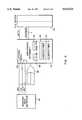
- FIG. 1An example of the Wash encoding method, as used to record data in bit streams in the MOF layer tracks described in the '419 patent, is shown in FIG. 1 which essentially reproduces FIG. 3 of the '139 patent.
- the Wash self-clocking bit codeis effected by the position of the positive going data signal level transition in the information-cell. If it is positioned within the first half of the duration of the information-cell, then a data bit 0 is recorded. Similarly, a data bit 1 is recorded by positioning the data transition in the second half of the information-cell.
- the data bitmay in fact be a parity bit, as the two terms are used below.
- the encoding of the information or data transitions for both the first and second information-cellsleaves invariant the clock transitions.
- film transport velocitycan vary during recording and playback without affecting the ability to synchronize and read the recorded data.
- the information-cellsmay lengthen or shorten depending on the filmstrip velocity, but the relative position of the data transitions can still be decoded.
- the camera disclosed in the '419 patentmay record data in the MOF layer tracks while winding the filmstrip between exposures without imposing any velocity controls or recording an independent clock track.
- large amounts of jitter in the camera transport at frequencies at or near the data frequenciesprecludes the use of a phase-locked loop in generating a clock during magnetic signal read out.
- the PPM information-cellsare decoded by means of a head sensitive to the field or rate of change of the flux emanating from the polarized regions at the transition zones.
- the signal produced by most magnetic reproduce headsis a voltage pulse corresponding to the location of a transition zone from one magnetically set region to another.
- the detection circuitry to which the head is attachedmust determine the location of one peak relative to another. This is most often done by differentiating the pulse and comparing the voltage to zero.
- the differentiated waveformwill cross zero at a time corresponding to the peak in the original waveform, at which point the comparator will change state. This works well in the region where the pulse has energy. However, outside this region, the input to the comparator hovers around zero, crossing zero as a result of noise, producing transitions at the output.
- the output of the comparatoris gated by a circuit which only allows the comparator state to change when the input waveform exceeds a threshold, usually 30%-45% of the peak amplitude.
- a thresholdusually 30%-45% of the peak amplitude.
- This schemeworks well in eliminating the unwanted transitions.
- a side effectis that, if the peak amplitude of the input signal fails to reach the threshold, no transition will occur and the data will be missed.
- Hard disk drivesdeal with this problem by marking locations on the disk where this occurs and not using the areas.
- Tape drivesuse frequent re-synching, read-while-write, re-reading, and powerful error correction code (ECC) to deal with the problem. Simple, inexpensive systems for use in cameras cannot use such complex and expensive solutions, and resort is therefor made to the self clocking PPM coding of Wash or Chi.
- a read/write magnetic head 12provides the read signals of FIG. 1B on lines 14.
- a pre-amplifier 16amplifies the output signal from the magnetic head 12 and applies the amplified signal on lines 26 to a filter 18 for removing an unnecessary component from the amplified read signals.
- a post-amplifier 20amplifies the filtered read signals and applies the filtered and amplified, positive and negative, signals to a peak detector 24 via line 22.
- the signalsare applied to a positive peak detector (NPD) 30 and a negative peak detector (PPD) 32 for detecting the negative and positive pulses having amplitudes exceeding respective threshold levels to ensure that noise signals are not decoded as data or clock signals.
- NPDpositive peak detector
- PPDnegative peak detector
- Uniform amplitude, polarity, and pulse width, clock and data, signal pulse trainsare thereby generated on lines 38 and 34 as depicted in FIG. 1C.
- a delay circuit 40is connected to the NPD 32 via line 38, resulting in a delayed clock pulse train on lines 46 and 48 and also appearing in FIG. 1C.
- the delayed clock signalis applied to the set terminal of the flip-flop 36 and is also applied to clear the up/down counter 50.
- the data signalis applied to the clear terminal of the flip-flop 36, so that the flip-flop 36 is set by delayed clock signals and cleared by data signals to provide the square wave signal shown in FIG. 1D at the Q output.
- the Q outputis set high by a delayed clock signal and low by the succeeding data signal.
- the up/down counter 50counts system clock 56 pulses applied to its CLK input, incrementing the count when the Q output is high and decrementing the count when the Q output is low.
- the most significant bit (MSB) of the output count of the up/down counter 50 and the CLOCK output from the NPD 32are supplied to a computer 42. The particular manner of determining the data bit in the information-cell is further explained in the '139 patent.
- the conventional data read out circuitcompares the absolute positive and negative amplitudes of the reproduced analog waveforms to threshold levels in the PPD and NPD circuits to convert, among the above-mentioned peaks, only the peaks having amplitudes higher than a predetermined threshold level into digital signals, determining that they are data bits 1 or 0 depending on their position in the case of the PPM encoded signals.
- the amplitudes of the pulse signalsfade below the thresholds, both the clock pulses separating successive information-cells and the data pulses signifying the binary data content can be lost.
- a block of three data bytes of eight information cellsis shown.
- the first bit of each byteis a parity bit (P i ), and the remaining seven bits are data bits (d i1 -d i7 ).
- P iparity bit
- d i1 -d i7data bits
- Each block of bytes recorded serially in a single track in the MOF layeris separated by a parity byte, called a Longitudinal Redundancy Check (LRC).
- LRCLongitudinal Redundancy Check
- Each vertical bit value of the LRCis calculated from the values of the data bits in its respective column.
- the data bits of successive information-cells in each blockare thereby protected with a 2-dimensional, horizontal and vertical, parity check in the data blocks. This scheme is able to correct an odd number of bits in error in any one byte, provided a bit is present at every position and the LRC is present in its proper position with the longitudinal parity bits lined up with their respective columns.
- the PPM encoding method described aboveincorporates the clock information in with the data so that a drop-out typically results in both loss of data content and loss of the clock signal.
- a drop-outoccurs, no clock is available to transmit data from the decoder to the memory, so that bits are completely missing in the recovered data block. This results in loss of byte synchronization and renders the parity checks useless in recovering the uncorrupted data. Shown below in table II is the situation after recovery when bits are lost:
- a method of and apparatus for decoding data from positive and negative pulses of an encoded pulse train, wherein the recorded data is subject to drop-outs and drop-inscomprises the steps of and means for: providing positive and negative peak pulse thresholds; comparing the magnitudes of positive and negative pulses to the positive and negative peak pulse thresholds; decoding data bits from valid positive and negative pulses exceeding the positive and negative peak pulse thresholds; identifying drop-outs in the encoded pulse train as a function of read out positive and negative pulse magnitudes not exceeding the positive and negative thresholds and providing drop-out flags in lieu of the respective positive and negative pulses; storing decoded data in memory locations; and storing the drop-out flags in memory locations in relation to decoded data such that the beginning and/or end of a drop-out in the encoded pulse train is indicated.
- the identifying step and meanspreferably further comprises the additional step of and means for identifying drop-outs or drop-ins in the encoded pulse train in response to the occurrence of two successive valid positive pulses or two successive valid negative pulses in the pulse train.
- the identifying step and meansmay further comprise the steps of and means for: timing out the interval between successive valid positive or negative pulses; providing a reference interval; comparing the timed out interval to the reference interval; and identifying drop-outs in the encoded pulse train in response to the timed out interval exceeding the reference interval.
- the drop-out flag storing step and meanspreferably further comprises the steps of and means for: identifying the preceding data stored decoded data location in memory; and storing the drop-out flag in a memory location in relation to the identified preceding decoded data location such that the last valid data prior to the beginning of the drop-out in the encoded pulse train is indicated.
- the present inventiondescribes a system that flags when a drop-out begins and/or ends in a memorized block of data. When used by the block decoder, the flags allows recovery of lost information.
- the identification of the beginning and/or end of a drop-outensures that the data is not misinterpreted and employed incorrectly, e.g. in processing a filmstrip having such encoded data recorded in the MOF layer tracks, for example.
- FIGS. 1A-1Eare waveform diagrams showing the recorded PPM information-cell clock and data signals of the prior art and the decoding of the data signals therefrom with the circuit of FIG. 2;
- FIG. 2depicts shows the prior art decoding circuit for decoding data and parity bits in information-cells in blocks of recorded data and parity bytes;
- FIG. 3A-3Fare waveform diagrams showing the decoding of recorded PPM information-cell clock and data signals and the identification of a drop-out and recover position in the decoded clock and data bit stream of any given block of bytes;
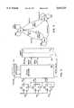
- FIG. 4is a modified peak detector in accordance with the present invention for detecting drop-outs and recovery in information-cells of FIG. 3A;
- FIG. 5is a system block diagram of a first embodiment of the invention coupled to the peak detector of FIG. 4 whereby the coded data is decoded and memorized and drop-outs or drop-ins are flagged in memory;
- FIG. 6is a flow chart depicting the general operation of the system of FIG. 5;
- FIG. 7is a detailed flow chart of the operation of the system of FIG. 5 for detecting drop-outs and drop-ins under a variety of circumstances;
- FIG. 8is an alternative embodiment of the invention employing a state machine coupled to the peak detector of FIG. 4 whereby the coded data is decoded and memorized and drop-outs or drop-ins are flagged in memory;
- FIG. 9is a state diagram illustrating the operation of the state machine of FIG. 8.
- the present inventionmay be implemented into a system for decoding the Wash, self clocking PPM signal levels in a read out circuit similar to that of FIG. 2 with modifications made to the peak detector 24 and incorporation of the operations of flip-flop 36, delay 40 and counter 50 into a microprocessor-based microcomputer.
- the modified peak detector 64includes a first PPD and NPD which detect peak signal levels that exceed (in absolute terms) the data and clock thresholds for decoding data and clock pulses and a second PPD and NPD which detect peak signal levels that exceed (in absolute terms) a lower threshold pair for detecting sub-threshold data and clock pulses occurring as the signal level drops out.
- the pulse signal waveformis inverted from those shown in FIG. 1B, but may be assumed to be equivalent thereto in function and with reversal of designations of the output signals of the PPDs and NPDs.
- the PPM encoded data bit patternis identified in FIG. 3B. A drop-out region is evidenced by the loss of amplitude of the pulse peaks.
- the positive clock pulse threshold CT+is augmented by a lower amplitude, positive clock drop-out pulse threshold CDT+.
- the negative data pulse threshold DT-is augmented by a higher amplitude, negative data drop-out pulse threshold DDT-.
- Any pulse peaks of the PPM signal falling in the positive or negative thresholdranges between the two sets of clock peak thresholds CT+ and CDT+ or data peak thresholds DDT- and DT- provides drop-out pulses DO+ or DO-, respectively, marking those peaks as bounding a drop-out region (as shown in FIG. 3D for DO+).
- Positive (clock) and negative (data) pulse peaks exceeding both thresholdsare indicated by peak detect pulse trains PD+ and PD- appearing in FIGS. 3C and 3E.
- the negative data pulse peaks in the drop-out zoneall fall below (in absolute terms) the data drop-out pulse threshold DDT-, and so none appear in FIG. 3F.
- the four thresholdsare set in the modified peak detector 64 of FIG. 4 by the reference voltages applied to input terminals of the modified PPD 70 and the modified NPD 72 which both receive the signal of FIG. 3A.
- Differentiator 74, comparator 76, and bi-directional one-shot 78form a modified peak detector 64 that outputs a timing pulse for each peak in the incoming signal waveform, regardless of polarity and amplitude. It will be understood that differentiator 74 may be replaced by an integrator or a non-linear peak detector of types known in the art having good signal-to-noise discrimination.
- the incoming signal waveformis applied to positive input terminals of comparators 92 and 94 of the modified PPD 70 and to the negative input terminals of comparators 104 and 106 of the modified NPD 72.
- the modified PPD 70 and NPD 72develop the pulse trains PD+ and PD- appearing in FIGS. 3C and 3E at the outputs of AND gates 80 and 82 or the pulse trains DO- and DO+ at the outputs of AND gates 84 and 86, except when the positive and negative signal peaks fall below both thresholds.
- the differentiator 74, comparator 76 and one shot 78are set to output the timing pulse near the positive or negative pulse signal peak such that the timing pulse duration falls within the duration of the output signals from comparators 92 and 104.
- First and second positive thresholdsare set by the resistor pair 88 and 90 between +Vref and system ground.
- the positive pulse threshold voltages CT+ and CDT+ developed therebyare applied to the negative input terminals of comparators 92 and 94, respectively.
- the output signal of comparator 92is applied to one input of AND gate 80 and to inverter 96, where it is inverted and applied to one input of AND gate 98.
- the output signal of comparator 94is applied to the other input of AND gate 98, and the output of AND gate 98 is applied to an input of AND gate 84.
- the other terminals of AND gates 80 and 84receive the timing pulse from one-shot 78.
- the negative threshold rangeis provided by the resistor pair 100 and 102 between -Vref and system ground.
- the negative threshold voltages DT- and DDT- developed therebyare applied to the positive input terminals of comparators 104 and 106, respectively.
- the output signal of comparator 104is applied to one input of AND gate 82 and to inverter 108, where it is inverted and applied to one input of AND gate 110.
- the output signal of comparator 102is applied to the other input of AND gate 110, and the output of AND gate 110 is applied to an input of AND gate 86.
- the other terminals of AND gates 82 and 86receive the timing pulse from one shot 78.
- comparators 92 and 104compare the first, upper (absolute value) threshold levels CT+ and DT- for a valid clock or data peak to the incoming read out signal pattern.
- Comparators 94 and 106compare the second, lower (absolute value) threshold levels CDT+ and DDT- to the incoming read out signal pattern shown in FIG. 3A.
- the timing pulseis developed from the differentiation and zero crossing detection of the peak magnitude of the read out signal pattern.
- comparators 92 and 94both go high at the point where their respective thresholds are exceeded.
- the positive pulse output of comparator 92 and the timing pulseare simultaneously applied to AND gate 80, allowing the peak detect pulse PD+ to be transmitted to the decoder.
- the inverted pulse from inverter 96disables AND gate 98 for the duration of the positive pulse output. Consequently, a pair of pulses may be passed by the AND gate 98 and applied to one input of AND gate 84 bracketing the timing pulse. Since the pulses do not overlap, the output of AND gate 84 does not go high and does not provide the drop-out pulse DO+. In this fashion, the decoding of the drop out pulse DO+ is inhibited or negated when the peak magnitude of the read out signal pattern exceeds the first and second thresholds CT+ and CDT+ and the decoding of the valid peak detect pulse PD+ is allowed.
- comparator 94applies its somewhat narrower high pulse output to AND gate 98 while the other input state is high, resulting in a high output applied to one input of AND gate 84 at the same time that the timing pulse is present at the other input. Therefore, the output of AND gate 84 goes high for the overlapping duration of the two pulses, resulting in the generation of the drop-out signal DO+ applied to the decoder.
- the NPD 72operates in a similar fashion to compare negative going data pulse signals to the third and fourth thresholds DT- and DDT- to develop either the PD- or DO- pulse signals of FIGS. 3E or 3F.
- the timing pulse generated by one-shot 78inhibits and negates the passage of drop-out pulse DO- through AND gate 86 when the magnitude of the negative, data peak exceeds the third threshold DT- and the peak detect pulse PD- is passed through gate 82.
- the second and fourth thresholds CDT+ and DDT-are set such that at least one positive or negative peak will fall in the positive or negative threshold range during either the onset or the end of a drop-out. This range will vary depending on the type of media and head used in the system.
- FIG. 5shows a specific implementation of a system for flagging any drop-out pulses DO+ or DO- that are generated by the modified peak detector 64 or drop-ins or drop-outs that elude the detector 64.
- the system of FIG. 5 operating as depicted in FIG. 7may also flag drop-ins or drop-outs from certain sequences of the peak detect pulses PD+ and PD-.
- the outputs of the AND gates 84 and 86are combined, and the combined drop-out pulses DO ⁇ , as well as the peak detect pulses PD+, PD- from the AND gates 80 and 82, are applied to a latched input 120 of a microprocessor 110.
- the outputs of the AND gates 80, 82 and 84/86are also applied to inputs of an OR gate 112 to provide an interrupt signal to tell the microprocessor 110 that one of the drop-out or peak detect pulses has been generated.
- the microprocessor 110could also poll the latched input 120 to detect the occurrence of a peak detect pulse PD+, PD- or drop-out pulse DO ⁇ .
- the microprocessor 110is programmed to store the most recent to occur of the peak detect pulse +PD, -PD, or drop-out pulse DO ⁇ in a 2-bit status register 118 for remembering the most recent pulse type.
- a first counter/timer 122 for decoding valid PPM datais also provided in the microprocessor 110.
- the first up/down counter/timer 122can be cleared to commence down counting and reversed to commence up counting on detection of a peak detect pulse -PD and a +PD, respectively.
- the count at the detection of a peak detect -PDis employed to decode a 1 or 0 data bit.
- a second counter timer 124is also provided for timing out intervals between successive clock peak detect pulses PD+ to detect drop-outs that may abruptly occur and not be detected in the modified peak detector 64 in a manner described below.
- the decoded bitsare applied on a data line to an n ⁇ 2 buffer 114 for storing the decoded data results.
- the buffer 114could be a small FIFO for temporary storage of results or it could be large enough to hold an entire frame of data.
- Buffer 114is two bits wide, because one bit is used for storing data bits and the other is used for storing drop-out flags.
- the buffer 114 and microprocessor 110may be combined in a microcomputer, of which many are commercially available.
- Microprocessor 110also has a memory pointer (mem ptr) register 116 which contains the address in the buffer 114 where the next decoded 1 or 0 bit and/or any drop-out or drop-in flag can be written.
- mem ptrmemory pointer
- the counter/timer 122may be counting up or down when a drop-out occurs and the count may bear no relation to the real data when the next data peak detect pulse -PD is detected
- the DO flags written in with the questionable data bitscan be used to identify the drop-outs.
- the counter/timer 122 of the microprocessor 110is operated in conjunction with the status bit register 118 to count up or down in a fashion analogous to the operation of the up/down counter 50 of FIG. 2.
- FIG. 6is a simplified flow chart of the decoding operation. Each time that a peak is detected in decision step S100, i.e., the interrupt is flagged in FIG. 5, the peak type is determined in decision step S102. If a positive clock peak detect pulse PD+ is at the latched input 120, the 1 or 0 bit sign is decoded as a function of the count in the counter/timer 122 following the decoding principles described above with respect to FIG. 1 and stored in buffer 114 in step S104. Then, in step S106, the count in the counter/timer 122 is cleared and count down is commenced again from the start count.
- step S108the counter/timer 122 is reversed in step S108 to count up from the down count value in the counter/timer 122. In this fashion, the resulting count in the counter/timer at the next clock peak detect pulse PD+ determines whether a 1 or 0 is decoded.
- DO flag bitsare set under a number of possible events, including the receipt of the drop-out DO ⁇ after either a peak detect pulse PD+ or PD-, as described above, or due to other indicators of a drop-out or a drop-in. Such indicators include the timeout of too great an interval between successive clock peak detect pulses PD+ indicating a drop-out and the detection of successive peak detect pulses of the same sign indicating a drop-in, if the timeout has not occurred, or a drop-out. Drop-out flags are set upon receipt of the first valid clock peak after an error condition. Moreover, an anticipatory drop-out flag may be recorded adjacent to the valid data bit stored just prior to determination of a drop-out or drop-in.
- the flow chart of FIG. 7commences with steps S200 and S202 corresponding to steps S100 and S102 of FIG. 6. A new path is added for discrimination of drop-out pulses DO ⁇ from the peak detect pulses +PD and -PD peaks to set the last peak state to a DO.
- the decision step S204determines if a +PD or DO ⁇ is at the respective latched input. If a DO ⁇ is at its latched input, then the last peak status register 118 is set in step S206 to DO, that is a condition which indicates that a drop-out has occurred since the last good data bit was detected.
- the count in the counter/timer 122continues to increment or decrement, and a DO flag is written into buffer 114 at the next positive clock peak detect pulse PD+ as described below.
- the status register 118is used to remember the polarity of the last valid peak detect pulse PD+ or PD- each time one is detected. If a peak detect pulse PD- rather than a DO is at the latched input 120, the status register 118 is queried at decision step S208. If the status register 118 stores a negative data peak detect pulse PD-, then the last peak status register is also set to DO in step S206. If, however, the last peak status register shows that the last peak pulse was not a negative peak detect pulse PD-, it is determined in decision step S210 whether it is storing a drop-out pulse DO. If it is not, then count direction in counter/timer 122 is reversed in step S212 (as in step S108 of FIG.
- step S200the last peak status register 118 stores the peak detect pulse PD-in block S214. If it is, then the counter/timer 122 count direction is not reversed, and the peak status register 118 continues to store the drop-out pulse DO. Then, the next interrupt is awaited in step S200.
- the further timer/counter 124 of microprocessor 110is operated to time out the intervals between successive clock peak detect pulses PD+ in step S216.
- the status of timer/counter 124is checked in the event that the positive, clock peak detect pulse PD+ is at the latched input in step S200.
- the timeris reset and the time out is stored in step S216, and the status register 118 is checked at step S218. If the last peak was a data peak detect pulse PD-, then the stored time is compared to a reference time related to the nominal clock interval of the information-cell in decision step S220.
- the DO flag bit of buffer 114is set in step S222, and it is stored in buffer 114 at the memory pointer designated stage adjacent to the empty decode data bit stage for the information-cell just ended by the detection of the clock peak detect pulse PD+. Since it would be desirable to flag the last valid data bit in buffer 114, the DO flag bit is set at the preceding memory pointer address in step S224. However, this step S224 need not be included in specific implementations of the algorithm.
- the last peak detect pulse PD-was stored in the status register 118, and the timer/counter 124 time out was not excessive, it can be assumed that the just ended information-cell was valid.
- the count in counter/timer 122is decoded and stored at the address in buffer 114 designated by the memory pointer 116 in step S226, and the memory pointer 116 is incremented to point to the next address in step S228.
- the counter/timer 122is cleared and the count down commenced in step S230, as in step S106 of FIG. 6.
- the last peak status register 118is again set to the clock peak detect pulse PD+ in step S232, and the interrupt is monitored in step S200.
- FIG. 7thus shows the use of the drop-out pulses DO ⁇ to mark the drop-out data bits in the buffer 114. Invalid data bits are not decoded, but the unique drop-out status can be identified.
- the flow chartalso employs other drop-out detectors in steps S216, S220 which could be eliminated from an operative embodiment.
- the flow chartshows the detection of successive peak detect pulses PD+ and PD- in steps S218 and S208, successively, which could be eliminated from an operative embodiment.
- itshows the flagging of the anticipatory drop-out in step S224 which could also be eliminated from an operative embodiment.
- FIGS. 8 and 9an alternative hardware implementation to the microprocessor based system of FIGS. 5-7 is depicted.
- a state machine 130is coupled to a buffer or shift register 132 for storing the decoded data bits and/or DO flags in response to the peak detect pulses PD+ and PD- and the drop-out pulses DO ⁇ in accordance with the operation of the state diagram of FIG. 9.
- the peak detect pulses PD+ and PD- and the drop-out pulses DO ⁇are applied to clock inputs of flip-flops 136, 138, 140 which are cleared by a common pulse applied to the reset inputs.
- a clockcontrols the operation of the state machine 130 and the up/down timer/counter 134 which provides the timing counts for decoding 1 or 0 data bits according to the PPM code described above.
- a logic 1is applied to the D inputs of the flip-flops 136, 138, 140 in common in order to set them on receipt of a pulse.
- the peak detect pulses PD+ and PD- and the drop-out pulses DO ⁇are applied as input states to the state machine 130 as long as the associated flip-flop state is high.
- a data valid outputis provided to notify succeeding circuitry that a valid data bit is available, that is, that a valid data bit has been shifted to the output of the shift register 132. The data and any drop-out flags are then shifted to a further register of the microprocessor-based system for data decoding and further processing.
- the state machine 130has four states with interconnected transitions and actions associated with the transitions designated A-H as shown in FIG. 9. Three primary states are designated by the state of the flip-flop inputs corresponding to the last received of the peak detect pulses PD+ and PD- and the drop-out pulse DO ⁇ . A fourth interim state "I" provides a delay so that the decoded bit in the MSB stage of counter 134 can be stored into the shift register 132 before it is shifted out.
- the input vector for each depicted state transitionis --PD+, PD-, DO--, which may be 000, 001, 010, or 100 for each depicted state transition.
- the state during the transition from the interim I state to the PD- stateis immaterial and is designated "XXX".
- the input vector 000is effected by the reset of the transitions.
- the transition actionsare stated as follows:
- the transition to the PD- stateis delayed at interim state I while the output data valid pulse is generated (F) and the shift out (H) takes place.
- the PD-stateis followed by a 010 input vector, the counter sign bit is not loaded, and the shift register DO bit is set (B). No state change occurs.
- the input vectoris reset, and the state is changed to DO.
- the DO statecan only be exited by an input vector 010 back to the PD- state.
- the transitionis accompanied by the input vector being reset (A), the shift register 132 being set to the DO bit (B), the counter 134 being cleared (C), and the count direction being set to Down (D).
- the state machine 130can be implemented to follow these states.
- the invention as described aboveis usable in any form of magnetic or optical recording or the like on any medium. Moreover, it may be used in any type of peak recording data coding other than the above described, NRZ or NRZI PPM code.
- a number of advantagesflow as a result of being able to detect the onset of a drop-out and/or the recovery or drop-in peak. Frequently, drop-outs of just a few bits occur, typically because of a momentary loss of contact of the head with the magnetic media as described above. In a typical clocked code, the number of missing bits can be determined. Once the number of bits are determined, the location in the stream of bytes can be determined.
- the bytes of a data blockare redundantly recorded, and the bytes located thereby having the drop-out bits can be ignored in favor of the back-up bytes.
- the corrupted data bytemay be reconstituted from the LRC and the byte parity bits P l . . . P n .
- a DO flag bitis associated with the positions corresponding to data bit d 24 and P 3 in the parallel bit-stage of the shift register 132 of FIG. 8 or the buffer 114 of FIG. 5.
- the bits following the drop-out code DOmay be shifted in Table IV until the parity bits of the parity column and data columns 1-4 are correct:
Landscapes
- Engineering & Computer Science (AREA)
- Signal Processing (AREA)
- Signal Processing For Digital Recording And Reproducing (AREA)
- Error Detection And Correction (AREA)
- Dc Digital Transmission (AREA)
- Compression, Expansion, Code Conversion, And Decoders (AREA)
Abstract
Description
______________________________________ Original Data ______________________________________ P.sub.1 d.sub.11 d.sub.12 d.sub.13 d.sub.14 d.sub.15 d.sub.16 d.sub.17 P.sub.2 d.sub.21 d.sub.22 d.sub.23 d.sub.24 d.sub.25 d.sub.26 d.sub.27 P.sub.3 d.sub.31 d.sub.32 d.sub.33 d.sub.34 d.sub.35 d.sub.36 d.sub.37 P P P P P P P P ______________________________________
______________________________________ Corrupted Data ______________________________________ P.sub.1 d.sub.11 d.sub.12 d.sub.13 d.sub.14 d.sub.15 d.sub.16 d.sub.17 P.sub.2 d.sub.21 d.sub.22 d.sub.23 d.sub.24 P.sub.3 d.sub.31 d.sub.32 d.sub.33 d.sub.34 d.sub.35 d.sub.36 d.sub.37 P P P P P P P P X X X ______________________________________
______________________________________ A Clear input vector B Setshift register 132 DO bit C Clear counter 134 D Set counter 134 count direction to Down E Set counter 134 count direction to Up F Output data valid pulse G Load counter sign bit toSR 132 data bit H Shift out ______________________________________
______________________________________ Corrupted Data ______________________________________ P.sub.1 d.sub.11 d.sub.12 d.sub.13 d.sub.14 d.sub.15 d.sub.16 d.sub.17 P.sub.2 d.sub.21 d.sub.22 d.sub.23 d.sub.24 P.sub.3 d.sub.31 d.sub.32 d.sub.33 d.sub.34 d.sub.35 d.sub.36 d.sub.37 P P P P P P P P X X X ______________________________________
______________________________________ Shifted Data ______________________________________ P.sub.1 d.sub.11 d.sub.12 d.sub.13 d.sub.14 d.sub.15 d.sub.16 d.sub.17 P.sub.2 d.sub.21 d.sub.22 d.sub.23 d.sub.24 X X X P.sub.3 d.sub.31 d.sub.32 d.sub.33 d.sub.34 d.sub.35 d.sub.36 d.sub.37 P P P P P P P P ______________________________________
Claims (18)
Priority Applications (3)
| Application Number | Priority Date | Filing Date | Title |
|---|---|---|---|
| US08/424,913US5615223A (en) | 1995-04-19 | 1995-04-19 | PPM decoder utilizing drop-out location information |
| JP8082357AJPH08293166A (en) | 1995-04-19 | 1996-04-04 | Method and apparatus for decoding of data |
| EP96106042AEP0739009A3 (en) | 1995-04-19 | 1996-04-18 | PPM decoder utilizing drop-out location information |
Applications Claiming Priority (1)
| Application Number | Priority Date | Filing Date | Title |
|---|---|---|---|
| US08/424,913US5615223A (en) | 1995-04-19 | 1995-04-19 | PPM decoder utilizing drop-out location information |
Publications (1)
| Publication Number | Publication Date |
|---|---|
| US5615223Atrue US5615223A (en) | 1997-03-25 |
Family
ID=23684407
Family Applications (1)
| Application Number | Title | Priority Date | Filing Date |
|---|---|---|---|
| US08/424,913Expired - LifetimeUS5615223A (en) | 1995-04-19 | 1995-04-19 | PPM decoder utilizing drop-out location information |
Country Status (3)
| Country | Link |
|---|---|
| US (1) | US5615223A (en) |
| EP (1) | EP0739009A3 (en) |
| JP (1) | JPH08293166A (en) |
Cited By (15)
| Publication number | Priority date | Publication date | Assignee | Title |
|---|---|---|---|---|
| US5949597A (en)* | 1996-04-24 | 1999-09-07 | Tandberg Data Storage A/S | Method and apparatus for data pulse qualification wherein the amplitude of a preceding pulse of opposite polarity is tracked |
| US6079045A (en)* | 1996-12-18 | 2000-06-20 | U.S. Philips Corporation | Transmission system and recording system having a simplified symbol detector |
| US6085270A (en)* | 1998-06-17 | 2000-07-04 | Advanced Micro Devices, Inc. | Multi-channel, multi-rate isochronous data bus |
| US6088748A (en)* | 1998-06-17 | 2000-07-11 | Advanced Micro Devices, Inc. | Personal computer system incorporating an isochronous multi-channel, multi-rate data bus |
| US6134698A (en)* | 1998-06-17 | 2000-10-17 | Advanced Micro Devices, Inc. | Reduced pin count isochronous data bus |
| US6167495A (en)* | 1998-08-27 | 2000-12-26 | Micron Technology, Inc. | Method and apparatus for detecting an initialization signal and a command packet error in packetized dynamic random access memories |
| US6404771B1 (en) | 1998-06-17 | 2002-06-11 | Advanced Micro Devices, Inc. | Clock lead/lag extraction in an isochronous data bus |
| US6731860B1 (en)* | 1998-04-15 | 2004-05-04 | Nippon Hoso Kyokai | Video reproduction controller for controlling reproduction of a recorded special video and a storage medium for the video reproduction controller |
| US20050050008A1 (en)* | 2000-07-24 | 2005-03-03 | Root Steven A. | Interactive advisory system |
| US20060161469A1 (en)* | 2005-01-14 | 2006-07-20 | Weatherbank, Inc. | Interactive advisory system |
| US20060178140A1 (en)* | 2005-02-02 | 2006-08-10 | Steven Smith | Location-based data communications system and method |
| US20080207183A1 (en)* | 2007-02-23 | 2008-08-28 | Weatherbank, Inc. | Interactive advisory system for prioritizing content |
| US20110230204A1 (en)* | 2006-01-19 | 2011-09-22 | Locator Ip, Lp | Interactive advisory system |
| US20160094211A1 (en)* | 2014-09-30 | 2016-03-31 | Ricoh Company, Ltd. | Voltage level detector, motor drive controller, motor apparatus, and method of detecting voltage level |
| CN115380512A (en)* | 2020-04-15 | 2022-11-22 | 高通股份有限公司 | Peak suppression information multiplexing on uplink shared channel |
Families Citing this family (1)
| Publication number | Priority date | Publication date | Assignee | Title |
|---|---|---|---|---|
| EP2921922B1 (en) | 2014-03-17 | 2018-06-20 | Rockwell Automation Limited | Method and apparatus for monitoring a signal |
Citations (23)
| Publication number | Priority date | Publication date | Assignee | Title |
|---|---|---|---|---|
| US3629823A (en)* | 1969-11-14 | 1971-12-21 | Gen Dynamics Corp | Information-handling system having error correction capabilities |
| US3715738A (en)* | 1970-10-19 | 1973-02-06 | Peripheral Business Equipment | Data detection system |
| US3840892A (en)* | 1972-07-07 | 1974-10-08 | Hitachi Ltd | Method and device for detecting signals from magnetic memory |
| US4025917A (en)* | 1975-11-06 | 1977-05-24 | The United States Of America As Represented By The Secretary Of The Navy | Simplified time code reader with digital PDM decoder |
| US4353130A (en)* | 1980-06-16 | 1982-10-05 | U.S. Philips Corporation | Device for processing serial information which includes synchronization words |
| US4449222A (en)* | 1981-11-23 | 1984-05-15 | Rockwell International Corporation | Digital modulation quality monitor |
| US4603357A (en)* | 1982-12-01 | 1986-07-29 | International Business Machines Corp. | Magnetic recording detection pointer that measures the time per data cell during which the analog waveform exceeds a predetermined detection threshold |
| US4613769A (en)* | 1984-08-13 | 1986-09-23 | National Semiconductor Corporation | Direct current coupled peak to peak detector circuit |
| US4964139A (en)* | 1989-04-27 | 1990-10-16 | Eastman Kodak Company | Multi-purpose circuit for decoding binary information |
| US4977419A (en)* | 1988-10-07 | 1990-12-11 | Eastman Kodak Company | Self-clocking encoding/decoding film information exchange system using dedicated magnetic tracks on film |
| US5020057A (en)* | 1988-12-05 | 1991-05-28 | Fujitsu Limited | Easy detection of head position of information data via reception processing unit in synchronous multiplex transmission apparatus |
| USRE33665E (en)* | 1981-12-08 | 1991-08-13 | Sony Corporation | Digital signal detecting and compensating circuit with adjustable window signal |
| US5089821A (en)* | 1988-05-28 | 1992-02-18 | Nec Corporation | Digital data reproducing circuit for a magnetic recording apparatus of reproducing digital data without being affected by capable external noise, drop-ins, and drop-outs |
| US5105316A (en)* | 1989-11-20 | 1992-04-14 | Seagate Technology, Inc. | Qualification for pulse detecting in a magnetic media data storage system |
| US5111485A (en)* | 1990-05-18 | 1992-05-05 | Northern Telecom Limited | Method of and circuit for synchronizing data |
| US5136591A (en)* | 1987-09-29 | 1992-08-04 | Siemens Aktiengesellschaft | Measuring method and device for fault analysis of digital transmission paths |
| US5148291A (en)* | 1986-05-21 | 1992-09-15 | Canon Kabushiki Kaisha | Apparatus for displaying image signal drop-out |
| US5199007A (en)* | 1990-02-08 | 1993-03-30 | Zexel Corporation | Compact watch dog timer circuit |
| US5293369A (en)* | 1992-10-28 | 1994-03-08 | International Business Machines Corporation | Asynchronous sampling digital detector system for magnetic and optical recording channels |
| US5301207A (en)* | 1992-04-03 | 1994-04-05 | Integrated Network Corporation | Test apparatus and process for digital data service system |
| US5313236A (en)* | 1991-11-28 | 1994-05-17 | Canon Kabushiki Kaisha | Demodulation processing circuit with time interval counting feature |
| US5345216A (en)* | 1993-02-26 | 1994-09-06 | Storage Technology Corporation | Method and apparatus for qualifying data peaks |
| US5455720A (en)* | 1991-10-01 | 1995-10-03 | Fujitsu Limited | Offset and gain error discriminator |
Family Cites Families (1)
| Publication number | Priority date | Publication date | Assignee | Title |
|---|---|---|---|---|
| DE3238077A1 (en)* | 1982-10-14 | 1984-04-19 | Basf Ag, 6700 Ludwigshafen | METHOD AND CIRCUIT ARRANGEMENTS FOR DETECTING AND EVALUATING DEFECTS ON RECORDING CARRIERS WITH DIGITAL SIGNALS RECORDED IN AT LEAST ONE TRACK |
- 1995
- 1995-04-19USUS08/424,913patent/US5615223A/ennot_activeExpired - Lifetime
- 1996
- 1996-04-04JPJP8082357Apatent/JPH08293166A/enactivePending
- 1996-04-18EPEP96106042Apatent/EP0739009A3/ennot_activeWithdrawn
Patent Citations (23)
| Publication number | Priority date | Publication date | Assignee | Title |
|---|---|---|---|---|
| US3629823A (en)* | 1969-11-14 | 1971-12-21 | Gen Dynamics Corp | Information-handling system having error correction capabilities |
| US3715738A (en)* | 1970-10-19 | 1973-02-06 | Peripheral Business Equipment | Data detection system |
| US3840892A (en)* | 1972-07-07 | 1974-10-08 | Hitachi Ltd | Method and device for detecting signals from magnetic memory |
| US4025917A (en)* | 1975-11-06 | 1977-05-24 | The United States Of America As Represented By The Secretary Of The Navy | Simplified time code reader with digital PDM decoder |
| US4353130A (en)* | 1980-06-16 | 1982-10-05 | U.S. Philips Corporation | Device for processing serial information which includes synchronization words |
| US4449222A (en)* | 1981-11-23 | 1984-05-15 | Rockwell International Corporation | Digital modulation quality monitor |
| USRE33665E (en)* | 1981-12-08 | 1991-08-13 | Sony Corporation | Digital signal detecting and compensating circuit with adjustable window signal |
| US4603357A (en)* | 1982-12-01 | 1986-07-29 | International Business Machines Corp. | Magnetic recording detection pointer that measures the time per data cell during which the analog waveform exceeds a predetermined detection threshold |
| US4613769A (en)* | 1984-08-13 | 1986-09-23 | National Semiconductor Corporation | Direct current coupled peak to peak detector circuit |
| US5148291A (en)* | 1986-05-21 | 1992-09-15 | Canon Kabushiki Kaisha | Apparatus for displaying image signal drop-out |
| US5136591A (en)* | 1987-09-29 | 1992-08-04 | Siemens Aktiengesellschaft | Measuring method and device for fault analysis of digital transmission paths |
| US5089821A (en)* | 1988-05-28 | 1992-02-18 | Nec Corporation | Digital data reproducing circuit for a magnetic recording apparatus of reproducing digital data without being affected by capable external noise, drop-ins, and drop-outs |
| US4977419A (en)* | 1988-10-07 | 1990-12-11 | Eastman Kodak Company | Self-clocking encoding/decoding film information exchange system using dedicated magnetic tracks on film |
| US5020057A (en)* | 1988-12-05 | 1991-05-28 | Fujitsu Limited | Easy detection of head position of information data via reception processing unit in synchronous multiplex transmission apparatus |
| US4964139A (en)* | 1989-04-27 | 1990-10-16 | Eastman Kodak Company | Multi-purpose circuit for decoding binary information |
| US5105316A (en)* | 1989-11-20 | 1992-04-14 | Seagate Technology, Inc. | Qualification for pulse detecting in a magnetic media data storage system |
| US5199007A (en)* | 1990-02-08 | 1993-03-30 | Zexel Corporation | Compact watch dog timer circuit |
| US5111485A (en)* | 1990-05-18 | 1992-05-05 | Northern Telecom Limited | Method of and circuit for synchronizing data |
| US5455720A (en)* | 1991-10-01 | 1995-10-03 | Fujitsu Limited | Offset and gain error discriminator |
| US5313236A (en)* | 1991-11-28 | 1994-05-17 | Canon Kabushiki Kaisha | Demodulation processing circuit with time interval counting feature |
| US5301207A (en)* | 1992-04-03 | 1994-04-05 | Integrated Network Corporation | Test apparatus and process for digital data service system |
| US5293369A (en)* | 1992-10-28 | 1994-03-08 | International Business Machines Corporation | Asynchronous sampling digital detector system for magnetic and optical recording channels |
| US5345216A (en)* | 1993-02-26 | 1994-09-06 | Storage Technology Corporation | Method and apparatus for qualifying data peaks |
Cited By (41)
| Publication number | Priority date | Publication date | Assignee | Title |
|---|---|---|---|---|
| US5949597A (en)* | 1996-04-24 | 1999-09-07 | Tandberg Data Storage A/S | Method and apparatus for data pulse qualification wherein the amplitude of a preceding pulse of opposite polarity is tracked |
| US6079045A (en)* | 1996-12-18 | 2000-06-20 | U.S. Philips Corporation | Transmission system and recording system having a simplified symbol detector |
| US6731860B1 (en)* | 1998-04-15 | 2004-05-04 | Nippon Hoso Kyokai | Video reproduction controller for controlling reproduction of a recorded special video and a storage medium for the video reproduction controller |
| US6085270A (en)* | 1998-06-17 | 2000-07-04 | Advanced Micro Devices, Inc. | Multi-channel, multi-rate isochronous data bus |
| US6088748A (en)* | 1998-06-17 | 2000-07-11 | Advanced Micro Devices, Inc. | Personal computer system incorporating an isochronous multi-channel, multi-rate data bus |
| US6134698A (en)* | 1998-06-17 | 2000-10-17 | Advanced Micro Devices, Inc. | Reduced pin count isochronous data bus |
| US6404771B1 (en) | 1998-06-17 | 2002-06-11 | Advanced Micro Devices, Inc. | Clock lead/lag extraction in an isochronous data bus |
| US6167495A (en)* | 1998-08-27 | 2000-12-26 | Micron Technology, Inc. | Method and apparatus for detecting an initialization signal and a command packet error in packetized dynamic random access memories |
| US6412052B2 (en) | 1998-08-27 | 2002-06-25 | Micron Technology, Inc. | Method and apparatus for detecting an initialization signal and a command packet error in packetized dynamic random access memories |
| US9661457B2 (en) | 2000-07-24 | 2017-05-23 | Locator Ip, Lp | Interactive advisory system |
| US9998295B2 (en) | 2000-07-24 | 2018-06-12 | Locator IP, L.P. | Interactive advisory system |
| US9560480B2 (en) | 2000-07-24 | 2017-01-31 | Locator Ip, Lp | Interactive advisory system |
| US20060294147A1 (en)* | 2000-07-24 | 2006-12-28 | Root Steven A | Interactive weather advisory system |
| US11108582B2 (en) | 2000-07-24 | 2021-08-31 | Locator IP, L.P. | Interactive weather advisory system |
| US10411908B2 (en) | 2000-07-24 | 2019-09-10 | Locator IP, L.P. | Interactive advisory system |
| US10021525B2 (en) | 2000-07-24 | 2018-07-10 | Locator IP, L.P. | Interactive weather advisory system |
| US9554246B2 (en) | 2000-07-24 | 2017-01-24 | Locator Ip, Lp | Interactive weather advisory system |
| US20050050008A1 (en)* | 2000-07-24 | 2005-03-03 | Root Steven A. | Interactive advisory system |
| US8909679B2 (en) | 2000-07-24 | 2014-12-09 | Locator Ip, Lp | Interactive advisory system |
| US9668091B2 (en) | 2000-07-24 | 2017-05-30 | Locator IP, L.P. | Interactive weather advisory system |
| US9191776B2 (en) | 2000-07-24 | 2015-11-17 | Locator Ip, Lp | Interactive advisory system |
| US9197990B2 (en) | 2000-07-24 | 2015-11-24 | Locator Ip, Lp | Interactive advisory system |
| US9204252B2 (en) | 2000-07-24 | 2015-12-01 | Locator IP, L.P. | Interactive advisory system |
| US20060161469A1 (en)* | 2005-01-14 | 2006-07-20 | Weatherbank, Inc. | Interactive advisory system |
| US11150378B2 (en) | 2005-01-14 | 2021-10-19 | Locator IP, L.P. | Method of outputting weather/environmental information from weather/environmental sensors |
| US8832121B2 (en)* | 2005-02-02 | 2014-09-09 | Accuweather, Inc. | Location-based data communications system and method |
| US20060178140A1 (en)* | 2005-02-02 | 2006-08-10 | Steven Smith | Location-based data communications system and method |
| US10362435B2 (en) | 2006-01-19 | 2019-07-23 | Locator IP, L.P. | Interactive advisory system |
| US8611927B2 (en) | 2006-01-19 | 2013-12-17 | Locator Ip, Lp | Interactive advisory system |
| US9215554B2 (en) | 2006-01-19 | 2015-12-15 | Locator IP, L.P. | Interactive advisory system |
| US9210541B2 (en) | 2006-01-19 | 2015-12-08 | Locator IP, L.P. | Interactive advisory system |
| US9094798B2 (en) | 2006-01-19 | 2015-07-28 | Locator IP, L.P. | Interactive advisory system |
| US20110230204A1 (en)* | 2006-01-19 | 2011-09-22 | Locator Ip, Lp | Interactive advisory system |
| US10021514B2 (en) | 2007-02-23 | 2018-07-10 | Locator IP, L.P. | Interactive advisory system for prioritizing content |
| US9237416B2 (en) | 2007-02-23 | 2016-01-12 | Locator IP, L.P. | Interactive advisory system for prioritizing content |
| US8634814B2 (en) | 2007-02-23 | 2014-01-21 | Locator IP, L.P. | Interactive advisory system for prioritizing content |
| US10616708B2 (en) | 2007-02-23 | 2020-04-07 | Locator Ip, Lp | Interactive advisory system for prioritizing content |
| US20080207183A1 (en)* | 2007-02-23 | 2008-08-28 | Weatherbank, Inc. | Interactive advisory system for prioritizing content |
| US20160094211A1 (en)* | 2014-09-30 | 2016-03-31 | Ricoh Company, Ltd. | Voltage level detector, motor drive controller, motor apparatus, and method of detecting voltage level |
| US9515641B2 (en)* | 2014-09-30 | 2016-12-06 | Ricoh Company, Ltd. | Voltage level detector, motor drive controller, motor apparatus, and method of detecting voltage level |
| CN115380512A (en)* | 2020-04-15 | 2022-11-22 | 高通股份有限公司 | Peak suppression information multiplexing on uplink shared channel |
Also Published As
| Publication number | Publication date |
|---|---|
| JPH08293166A (en) | 1996-11-05 |
| EP0739009A3 (en) | 1998-01-07 |
| EP0739009A2 (en) | 1996-10-23 |
Similar Documents
| Publication | Publication Date | Title |
|---|---|---|
| US5615223A (en) | PPM decoder utilizing drop-out location information | |
| US8379340B2 (en) | Circuit and method for detecting the phase of a servo signal | |
| JP3428039B2 (en) | Synchronous signal detector, synchronous signal detecting method and decoding device | |
| US4183066A (en) | Technique for recording data on magnetic disks at plural densities | |
| JP3170123B2 (en) | Error correction circuit | |
| US5105316A (en) | Qualification for pulse detecting in a magnetic media data storage system | |
| US5627846A (en) | Drop-out location detection circuit | |
| JPH06162668A (en) | Information recording system | |
| CA1156360A (en) | Video disc apparatus for clearing foreign matter from the signal pickup stylus during playback | |
| KR910003378B1 (en) | Digital signal demodulation and playing device | |
| WO1994012981A1 (en) | Head switching method for staggered servo and circuit thereof | |
| JPH04159664A (en) | Magnetic recording/reproduction device | |
| US5436881A (en) | Method and apparatus for detecting pulse signal for generating clock from recording medium | |
| JPH0656700B2 (en) | Decoding device for a record carrier provided with a multi-track data pattern containing error prevention data and reproducing device having such a decoding device | |
| US3706084A (en) | Mass memory system | |
| JP2560047Y2 (en) | Abnormal block discrimination mechanism of magnetic tape recording and reproducing device | |
| KR100250577B1 (en) | Apparatus for detecting synchronous signal of video cd | |
| KR100324763B1 (en) | Tape performance testing method and apparatus for digital signal recording and reproducing apparatus | |
| EP0952579A2 (en) | Information reproduction apparatus | |
| KR100213020B1 (en) | Frame synchronization signal detection device and frame signal detection device for reproducing magneto-optical disk signal using same | |
| JPH0346167A (en) | Demodulation circuit | |
| JPH0346166A (en) | Demodulation circuit | |
| JPS62217747A (en) | Synchronization detection device | |
| JPH06139727A (en) | Magnetic disk and magnetic disk device | |
| JPH01128207A (en) | Error pointer generation circuit for magnetic recording/reproducing device |
Legal Events
| Date | Code | Title | Description |
|---|---|---|---|
| AS | Assignment | Owner name:EASTMAN KODAK COMPANY, NEW YORK Free format text:ASSIGNMENT OF ASSIGNORS INTEREST;ASSIGNOR:CARR, THOMAS D.;REEL/FRAME:007442/0423 Effective date:19950410 | |
| FEPP | Fee payment procedure | Free format text:PAYOR NUMBER ASSIGNED (ORIGINAL EVENT CODE: ASPN); ENTITY STATUS OF PATENT OWNER: LARGE ENTITY | |
| STCF | Information on status: patent grant | Free format text:PATENTED CASE | |
| FEPP | Fee payment procedure | Free format text:PAYER NUMBER DE-ASSIGNED (ORIGINAL EVENT CODE: RMPN); ENTITY STATUS OF PATENT OWNER: LARGE ENTITY | |
| REFU | Refund | Free format text:REFUND - PAYMENT OF MAINTENANCE FEE, 4TH YR, SMALL ENTITY (ORIGINAL EVENT CODE: R283); ENTITY STATUS OF PATENT OWNER: LARGE ENTITY | |
| FEPP | Fee payment procedure | Free format text:PAT HLDR NO LONGER CLAIMS SMALL ENT STAT AS SMALL BUSINESS (ORIGINAL EVENT CODE: LSM2); ENTITY STATUS OF PATENT OWNER: LARGE ENTITY | |
| FPAY | Fee payment | Year of fee payment:4 | |
| FEPP | Fee payment procedure | Free format text:PAYOR NUMBER ASSIGNED (ORIGINAL EVENT CODE: ASPN); ENTITY STATUS OF PATENT OWNER: LARGE ENTITY | |
| FPAY | Fee payment | Year of fee payment:8 | |
| FPAY | Fee payment | Year of fee payment:12 | |
| AS | Assignment | Owner name:CITICORP NORTH AMERICA, INC., AS AGENT, NEW YORK Free format text:SECURITY INTEREST;ASSIGNORS:EASTMAN KODAK COMPANY;PAKON, INC.;REEL/FRAME:028201/0420 Effective date:20120215 | |
| AS | Assignment | Owner name:WILMINGTON TRUST, NATIONAL ASSOCIATION, AS AGENT, MINNESOTA Free format text:PATENT SECURITY AGREEMENT;ASSIGNORS:EASTMAN KODAK COMPANY;PAKON, INC.;REEL/FRAME:030122/0235 Effective date:20130322 Owner name:WILMINGTON TRUST, NATIONAL ASSOCIATION, AS AGENT, Free format text:PATENT SECURITY AGREEMENT;ASSIGNORS:EASTMAN KODAK COMPANY;PAKON, INC.;REEL/FRAME:030122/0235 Effective date:20130322 | |
| AS | Assignment | Owner name:JPMORGAN CHASE BANK, N.A., AS ADMINISTRATIVE, DELAWARE Free format text:INTELLECTUAL PROPERTY SECURITY AGREEMENT (FIRST LIEN);ASSIGNORS:EASTMAN KODAK COMPANY;FAR EAST DEVELOPMENT LTD.;FPC INC.;AND OTHERS;REEL/FRAME:031158/0001 Effective date:20130903 Owner name:BARCLAYS BANK PLC, AS ADMINISTRATIVE AGENT, NEW YORK Free format text:INTELLECTUAL PROPERTY SECURITY AGREEMENT (SECOND LIEN);ASSIGNORS:EASTMAN KODAK COMPANY;FAR EAST DEVELOPMENT LTD.;FPC INC.;AND OTHERS;REEL/FRAME:031159/0001 Effective date:20130903 Owner name:JPMORGAN CHASE BANK, N.A., AS ADMINISTRATIVE, DELA Free format text:INTELLECTUAL PROPERTY SECURITY AGREEMENT (FIRST LIEN);ASSIGNORS:EASTMAN KODAK COMPANY;FAR EAST DEVELOPMENT LTD.;FPC INC.;AND OTHERS;REEL/FRAME:031158/0001 Effective date:20130903 Owner name:PAKON, INC., NEW YORK Free format text:RELEASE OF SECURITY INTEREST IN PATENTS;ASSIGNORS:CITICORP NORTH AMERICA, INC., AS SENIOR DIP AGENT;WILMINGTON TRUST, NATIONAL ASSOCIATION, AS JUNIOR DIP AGENT;REEL/FRAME:031157/0451 Effective date:20130903 Owner name:EASTMAN KODAK COMPANY, NEW YORK Free format text:RELEASE OF SECURITY INTEREST IN PATENTS;ASSIGNORS:CITICORP NORTH AMERICA, INC., AS SENIOR DIP AGENT;WILMINGTON TRUST, NATIONAL ASSOCIATION, AS JUNIOR DIP AGENT;REEL/FRAME:031157/0451 Effective date:20130903 Owner name:BARCLAYS BANK PLC, AS ADMINISTRATIVE AGENT, NEW YO Free format text:INTELLECTUAL PROPERTY SECURITY AGREEMENT (SECOND LIEN);ASSIGNORS:EASTMAN KODAK COMPANY;FAR EAST DEVELOPMENT LTD.;FPC INC.;AND OTHERS;REEL/FRAME:031159/0001 Effective date:20130903 Owner name:BANK OF AMERICA N.A., AS AGENT, MASSACHUSETTS Free format text:INTELLECTUAL PROPERTY SECURITY AGREEMENT (ABL);ASSIGNORS:EASTMAN KODAK COMPANY;FAR EAST DEVELOPMENT LTD.;FPC INC.;AND OTHERS;REEL/FRAME:031162/0117 Effective date:20130903 | |
| AS | Assignment | Owner name:EASTMAN KODAK COMPANY, NEW YORK Free format text:RELEASE BY SECURED PARTY;ASSIGNOR:BARCLAYS BANK PLC;REEL/FRAME:041656/0531 Effective date:20170202 | |
| AS | Assignment | Owner name:KODAK PORTUGUESA LIMITED, NEW YORK Free format text:RELEASE BY SECURED PARTY;ASSIGNOR:JP MORGAN CHASE BANK, N.A., AS ADMINISTRATIVE AGENT;REEL/FRAME:049814/0001 Effective date:20190617 Owner name:FAR EAST DEVELOPMENT LTD., NEW YORK Free format text:RELEASE BY SECURED PARTY;ASSIGNOR:JP MORGAN CHASE BANK, N.A., AS ADMINISTRATIVE AGENT;REEL/FRAME:049814/0001 Effective date:20190617 Owner name:KODAK (NEAR EAST), INC., NEW YORK Free format text:RELEASE BY SECURED PARTY;ASSIGNOR:JP MORGAN CHASE BANK, N.A., AS ADMINISTRATIVE AGENT;REEL/FRAME:049814/0001 Effective date:20190617 Owner name:KODAK REALTY, INC., NEW YORK Free format text:RELEASE BY SECURED PARTY;ASSIGNOR:JP MORGAN CHASE BANK, N.A., AS ADMINISTRATIVE AGENT;REEL/FRAME:049814/0001 Effective date:20190617 Owner name:KODAK AVIATION LEASING LLC, NEW YORK Free format text:RELEASE BY SECURED PARTY;ASSIGNOR:JP MORGAN CHASE BANK, N.A., AS ADMINISTRATIVE AGENT;REEL/FRAME:049814/0001 Effective date:20190617 Owner name:KODAK PHILIPPINES, LTD., NEW YORK Free format text:RELEASE BY SECURED PARTY;ASSIGNOR:JP MORGAN CHASE BANK, N.A., AS ADMINISTRATIVE AGENT;REEL/FRAME:049814/0001 Effective date:20190617 Owner name:NPEC, INC., NEW YORK Free format text:RELEASE BY SECURED PARTY;ASSIGNOR:JP MORGAN CHASE BANK, N.A., AS ADMINISTRATIVE AGENT;REEL/FRAME:049814/0001 Effective date:20190617 Owner name:LASER PACIFIC MEDIA CORPORATION, NEW YORK Free format text:RELEASE BY SECURED PARTY;ASSIGNOR:JP MORGAN CHASE BANK, N.A., AS ADMINISTRATIVE AGENT;REEL/FRAME:049814/0001 Effective date:20190617 Owner name:CREO MANUFACTURING AMERICA LLC, NEW YORK Free format text:RELEASE BY SECURED PARTY;ASSIGNOR:JP MORGAN CHASE BANK, N.A., AS ADMINISTRATIVE AGENT;REEL/FRAME:049814/0001 Effective date:20190617 Owner name:PAKON, INC., NEW YORK Free format text:RELEASE BY SECURED PARTY;ASSIGNOR:JP MORGAN CHASE BANK, N.A., AS ADMINISTRATIVE AGENT;REEL/FRAME:049814/0001 Effective date:20190617 Owner name:KODAK IMAGING NETWORK, INC., NEW YORK Free format text:RELEASE BY SECURED PARTY;ASSIGNOR:JP MORGAN CHASE BANK, N.A., AS ADMINISTRATIVE AGENT;REEL/FRAME:049814/0001 Effective date:20190617 Owner name:FPC, INC., NEW YORK Free format text:RELEASE BY SECURED PARTY;ASSIGNOR:JP MORGAN CHASE BANK, N.A., AS ADMINISTRATIVE AGENT;REEL/FRAME:049814/0001 Effective date:20190617 Owner name:QUALEX, INC., NEW YORK Free format text:RELEASE BY SECURED PARTY;ASSIGNOR:JP MORGAN CHASE BANK, N.A., AS ADMINISTRATIVE AGENT;REEL/FRAME:049814/0001 Effective date:20190617 Owner name:EASTMAN KODAK COMPANY, NEW YORK Free format text:RELEASE BY SECURED PARTY;ASSIGNOR:JP MORGAN CHASE BANK, N.A., AS ADMINISTRATIVE AGENT;REEL/FRAME:049814/0001 Effective date:20190617 Owner name:KODAK AMERICAS, LTD., NEW YORK Free format text:RELEASE BY SECURED PARTY;ASSIGNOR:JP MORGAN CHASE BANK, N.A., AS ADMINISTRATIVE AGENT;REEL/FRAME:049814/0001 Effective date:20190617 | |
| AS | Assignment | Owner name:KODAK PHILIPPINES LTD., NEW YORK Free format text:RELEASE BY SECURED PARTY;ASSIGNOR:BARCLAYS BANK PLC;REEL/FRAME:052773/0001 Effective date:20170202 Owner name:KODAK REALTY INC., NEW YORK Free format text:RELEASE BY SECURED PARTY;ASSIGNOR:BARCLAYS BANK PLC;REEL/FRAME:052773/0001 Effective date:20170202 Owner name:FAR EAST DEVELOPMENT LTD., NEW YORK Free format text:RELEASE BY SECURED PARTY;ASSIGNOR:BARCLAYS BANK PLC;REEL/FRAME:052773/0001 Effective date:20170202 Owner name:QUALEX INC., NEW YORK Free format text:RELEASE BY SECURED PARTY;ASSIGNOR:BARCLAYS BANK PLC;REEL/FRAME:052773/0001 Effective date:20170202 Owner name:EASTMAN KODAK COMPANY, NEW YORK Free format text:RELEASE BY SECURED PARTY;ASSIGNOR:BARCLAYS BANK PLC;REEL/FRAME:052773/0001 Effective date:20170202 Owner name:NPEC INC., NEW YORK Free format text:RELEASE BY SECURED PARTY;ASSIGNOR:BARCLAYS BANK PLC;REEL/FRAME:052773/0001 Effective date:20170202 Owner name:LASER PACIFIC MEDIA CORPORATION, NEW YORK Free format text:RELEASE BY SECURED PARTY;ASSIGNOR:BARCLAYS BANK PLC;REEL/FRAME:052773/0001 Effective date:20170202 Owner name:KODAK (NEAR EAST) INC., NEW YORK Free format text:RELEASE BY SECURED PARTY;ASSIGNOR:BARCLAYS BANK PLC;REEL/FRAME:052773/0001 Effective date:20170202 Owner name:KODAK AMERICAS LTD., NEW YORK Free format text:RELEASE BY SECURED PARTY;ASSIGNOR:BARCLAYS BANK PLC;REEL/FRAME:052773/0001 Effective date:20170202 Owner name:FPC INC., NEW YORK Free format text:RELEASE BY SECURED PARTY;ASSIGNOR:BARCLAYS BANK PLC;REEL/FRAME:052773/0001 Effective date:20170202 |