US5614437A - Method for fabricating reliable metallization with Ta-Si-N barrier for semiconductors - Google Patents
Method for fabricating reliable metallization with Ta-Si-N barrier for semiconductorsDownload PDFInfo
- Publication number
- US5614437A US5614437AUS08/378,750US37875095AUS5614437AUS 5614437 AUS5614437 AUS 5614437AUS 37875095 AUS37875095 AUS 37875095AUS 5614437 AUS5614437 AUS 5614437A
- Authority
- US
- United States
- Prior art keywords
- layer
- recited
- depositing
- metallization
- ohmic contact
- Prior art date
- Legal status (The legal status is an assumption and is not a legal conclusion. Google has not performed a legal analysis and makes no representation as to the accuracy of the status listed.)
- Expired - Lifetime
Links
- 238000001465metallisationMethods0.000titleclaimsabstractdescription77
- 238000000034methodMethods0.000titleclaimsabstractdescription60
- 230000004888barrier functionEffects0.000titleclaimsabstractdescription48
- 239000004065semiconductorSubstances0.000titleclaimsabstractdescription37
- 229910007991Si-NInorganic materials0.000title1
- 229910006294Si—NInorganic materials0.000title1
- 238000000151depositionMethods0.000claimsabstractdescription41
- 230000008021depositionEffects0.000claimsabstractdescription21
- HWEYZGSCHQNNEH-UHFFFAOYSA-Nsilicon tantalumChemical compound[Si].[Ta]HWEYZGSCHQNNEH-UHFFFAOYSA-N0.000claimsabstractdescription21
- 229910052581Si3N4Inorganic materials0.000claimsabstractdescription17
- 229910052715tantalumInorganic materials0.000claimsabstractdescription15
- GUVRBAGPIYLISA-UHFFFAOYSA-Ntantalum atomChemical compound[Ta]GUVRBAGPIYLISA-UHFFFAOYSA-N0.000claimsabstractdescription14
- 238000004519manufacturing processMethods0.000claimsabstractdescription11
- 229910052710siliconInorganic materials0.000claimsabstractdescription11
- 239000010703siliconSubstances0.000claimsabstractdescription11
- 238000005530etchingMethods0.000claimsabstractdescription7
- 239000000758substrateSubstances0.000claimsdescription25
- 238000009736wettingMethods0.000claimsdescription12
- 229910052782aluminiumInorganic materials0.000claimsdescription11
- XAGFODPZIPBFFR-UHFFFAOYSA-NaluminiumChemical group[Al]XAGFODPZIPBFFR-UHFFFAOYSA-N0.000claimsdescription11
- XUIMIQQOPSSXEZ-UHFFFAOYSA-NSiliconChemical compound[Si]XUIMIQQOPSSXEZ-UHFFFAOYSA-N0.000claimsdescription10
- 230000003667anti-reflective effectEffects0.000claimsdescription10
- 238000005546reactive sputteringMethods0.000claimsdescription7
- 229910021332silicideInorganic materials0.000claimsdescription5
- FVBUAEGBCNSCDD-UHFFFAOYSA-Nsilicide(4-)Chemical compound[Si-4]FVBUAEGBCNSCDD-UHFFFAOYSA-N0.000claimsdescription5
- XKRFYHLGVUSROY-UHFFFAOYSA-NArgonChemical compound[Ar]XKRFYHLGVUSROY-UHFFFAOYSA-N0.000claimsdescription4
- 229910045601alloyInorganic materials0.000claimsdescription3
- 239000000956alloySubstances0.000claimsdescription3
- 229910052786argonInorganic materials0.000claimsdescription2
- IJGRMHOSHXDMSA-UHFFFAOYSA-NAtomic nitrogenChemical compoundN#NIJGRMHOSHXDMSA-UHFFFAOYSA-N0.000claims2
- 229910052757nitrogenInorganic materials0.000claims1
- 238000001020plasma etchingMethods0.000claims1
- 229910000838Al alloyInorganic materials0.000abstractdescription4
- 238000004544sputter depositionMethods0.000abstractdescription3
- 239000012300argon atmosphereSubstances0.000abstractdescription2
- 230000008569processEffects0.000description27
- 238000009792diffusion processMethods0.000description12
- 229910052721tungstenInorganic materials0.000description10
- 239000010936titaniumSubstances0.000description9
- WFKWXMTUELFFGS-UHFFFAOYSA-NtungstenChemical compound[W]WFKWXMTUELFFGS-UHFFFAOYSA-N0.000description9
- 239000010937tungstenSubstances0.000description9
- NRTOMJZYCJJWKI-UHFFFAOYSA-NTitanium nitrideChemical compound[Ti]#NNRTOMJZYCJJWKI-UHFFFAOYSA-N0.000description7
- 239000000463materialSubstances0.000description6
- 229910052751metalInorganic materials0.000description6
- 239000002184metalSubstances0.000description6
- RTAQQCXQSZGOHL-UHFFFAOYSA-NTitaniumChemical compound[Ti]RTAQQCXQSZGOHL-UHFFFAOYSA-N0.000description5
- 238000000637aluminium metallisationMethods0.000description5
- 229910052719titaniumInorganic materials0.000description5
- 239000010949copperSubstances0.000description4
- RYGMFSIKBFXOCR-UHFFFAOYSA-NCopperChemical compound[Cu]RYGMFSIKBFXOCR-UHFFFAOYSA-N0.000description3
- 239000005380borophosphosilicate glassSubstances0.000description3
- 229910052802copperInorganic materials0.000description3
- 230000003247decreasing effectEffects0.000description2
- 238000005516engineering processMethods0.000description2
- 239000000075oxide glassSubstances0.000description2
- 238000002161passivationMethods0.000description2
- 229910021341titanium silicideInorganic materials0.000description2
- 230000008901benefitEffects0.000description1
- 230000015572biosynthetic processEffects0.000description1
- 230000002860competitive effectEffects0.000description1
- 239000004020conductorSubstances0.000description1
- 230000002950deficientEffects0.000description1
- 230000000593degrading effectEffects0.000description1
- 239000003989dielectric materialSubstances0.000description1
- 238000011156evaluationMethods0.000description1
- 239000011521glassSubstances0.000description1
- 239000012212insulatorSubstances0.000description1
- 230000008018meltingEffects0.000description1
- 238000002844meltingMethods0.000description1
- 239000000203mixtureSubstances0.000description1
- 229910052750molybdenumInorganic materials0.000description1
- 239000012299nitrogen atmosphereSubstances0.000description1
- 238000004806packaging method and processMethods0.000description1
- 238000012856packingMethods0.000description1
- 230000037361pathwayEffects0.000description1
- 238000000059patterningMethods0.000description1
- 238000005498polishingMethods0.000description1
- 230000009467reductionEffects0.000description1
- 238000007493shaping processMethods0.000description1
- 238000000742single-metal depositionMethods0.000description1
- 238000004513sizingMethods0.000description1
- 239000007787solidSubstances0.000description1
- 125000006850spacer groupChemical group0.000description1
Images


Classifications
- H—ELECTRICITY
- H01—ELECTRIC ELEMENTS
- H01L—SEMICONDUCTOR DEVICES NOT COVERED BY CLASS H10
- H01L21/00—Processes or apparatus adapted for the manufacture or treatment of semiconductor or solid state devices or of parts thereof
- H01L21/70—Manufacture or treatment of devices consisting of a plurality of solid state components formed in or on a common substrate or of parts thereof; Manufacture of integrated circuit devices or of parts thereof
- H01L21/71—Manufacture of specific parts of devices defined in group H01L21/70
- H01L21/768—Applying interconnections to be used for carrying current between separate components within a device comprising conductors and dielectrics
- H01L21/76838—Applying interconnections to be used for carrying current between separate components within a device comprising conductors and dielectrics characterised by the formation and the after-treatment of the conductors
- H01L21/76841—Barrier, adhesion or liner layers
- H01L21/76843—Barrier, adhesion or liner layers formed in openings in a dielectric
- H01L21/76846—Layer combinations
- H—ELECTRICITY
- H01—ELECTRIC ELEMENTS
- H01L—SEMICONDUCTOR DEVICES NOT COVERED BY CLASS H10
- H01L21/00—Processes or apparatus adapted for the manufacture or treatment of semiconductor or solid state devices or of parts thereof
- H01L21/70—Manufacture or treatment of devices consisting of a plurality of solid state components formed in or on a common substrate or of parts thereof; Manufacture of integrated circuit devices or of parts thereof
- H01L21/71—Manufacture of specific parts of devices defined in group H01L21/70
- H01L21/768—Applying interconnections to be used for carrying current between separate components within a device comprising conductors and dielectrics
- H01L21/76838—Applying interconnections to be used for carrying current between separate components within a device comprising conductors and dielectrics characterised by the formation and the after-treatment of the conductors
- H01L21/76841—Barrier, adhesion or liner layers
- H01L21/76843—Barrier, adhesion or liner layers formed in openings in a dielectric
- H—ELECTRICITY
- H01—ELECTRIC ELEMENTS
- H01L—SEMICONDUCTOR DEVICES NOT COVERED BY CLASS H10
- H01L23/00—Details of semiconductor or other solid state devices
- H01L23/52—Arrangements for conducting electric current within the device in operation from one component to another, i.e. interconnections, e.g. wires, lead frames
- H01L23/522—Arrangements for conducting electric current within the device in operation from one component to another, i.e. interconnections, e.g. wires, lead frames including external interconnections consisting of a multilayer structure of conductive and insulating layers inseparably formed on the semiconductor body
- H01L23/532—Arrangements for conducting electric current within the device in operation from one component to another, i.e. interconnections, e.g. wires, lead frames including external interconnections consisting of a multilayer structure of conductive and insulating layers inseparably formed on the semiconductor body characterised by the materials
- H01L23/53204—Conductive materials
- H01L23/53209—Conductive materials based on metals, e.g. alloys, metal silicides
- H01L23/53214—Conductive materials based on metals, e.g. alloys, metal silicides the principal metal being aluminium
- H01L23/53223—Additional layers associated with aluminium layers, e.g. adhesion, barrier, cladding layers
- H—ELECTRICITY
- H10—SEMICONDUCTOR DEVICES; ELECTRIC SOLID-STATE DEVICES NOT OTHERWISE PROVIDED FOR
- H10D—INORGANIC ELECTRIC SEMICONDUCTOR DEVICES
- H10D62/00—Semiconductor bodies, or regions thereof, of devices having potential barriers
- H10D62/80—Semiconductor bodies, or regions thereof, of devices having potential barriers characterised by the materials
- H10D62/83—Semiconductor bodies, or regions thereof, of devices having potential barriers characterised by the materials being Group IV materials, e.g. B-doped Si or undoped Ge
- H—ELECTRICITY
- H10—SEMICONDUCTOR DEVICES; ELECTRIC SOLID-STATE DEVICES NOT OTHERWISE PROVIDED FOR
- H10D—INORGANIC ELECTRIC SEMICONDUCTOR DEVICES
- H10D64/00—Electrodes of devices having potential barriers
- H10D64/60—Electrodes characterised by their materials
- H10D64/62—Electrodes ohmically coupled to a semiconductor
- H—ELECTRICITY
- H01—ELECTRIC ELEMENTS
- H01L—SEMICONDUCTOR DEVICES NOT COVERED BY CLASS H10
- H01L2924/00—Indexing scheme for arrangements or methods for connecting or disconnecting semiconductor or solid-state bodies as covered by H01L24/00
- H01L2924/0001—Technical content checked by a classifier
- H01L2924/0002—Not covered by any one of groups H01L24/00, H01L24/00 and H01L2224/00
Definitions
- the present inventionrelates generally to methods of forming ohmic contacts between metallization layers and device elements in semiconductor devices. More particularly, the invention relates to methods of forming contacts that include tantalum-containing barrier layers.
- a conductive metalsuch as aluminum or an aluminum alloy
- the interconnectionsare electrically conductive paths between various device elements of the devices making up the integrated circuit. Each such device element must make an ohmic contact with an interconnection.
- device elements requiring ohmic contacts to metal interconnectsinclude sources, drains, and gate electrodes.
- the well regions in which MOS devices are formedgenerally require ohmic contacts to metal interconnections.
- the process of depositing the conductive metalis termed “contact metallization” or simply “metallization”.
- the conductive metal layeris called a “metallization layer”.
- an insulating or dielectric "blanket” layeris deposited over the substrate, thereby covering any device elements which require electrical connection. Thereafter, to enable electrical connection to these devices, interconnect regions, called “contact vias” or simply “vias", are etched through the blanket layer and expose portions of the device elements. After a few intervening steps (discussed below), a metallization layer is deposited. To successfully form ohmic contacts, the metallization layer (or some other electrically conductive material) must extend down into and conformally fill the contact vias. Otherwise gaps may remain in the via and prevent reliable electrical contact. Thus, the process steps and conditions must be conducted under conditions which provide adequate filling of the vias.
- a diffusion barrieris formed over the top of the insulating layer. This is to prevent species from the metallization (often copper present in the aluminum metallization) from diffusing into the substrate and degrading device performance.
- diffusion barriersare made from materials which prevent diffusion while still allowing good electrical contact between the metallization layer and the substrate.
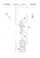
- a silicon substrate 20includes a source region 22, a gate electrode 24, and a drain region 26.
- a non-conductive blanket layer 30comprised of a low temperature oxide/borophosphosilicate glass is conformally deposited on substrate 20.
- a viais etched through the blanket layer 30, thereby exposing a portion of the source region 22. It should be noted that in actual processes, vias are simultaneously formed over gates, drain regions, source regions, and well regions. To simplify illustration, however, only the source region via will be shown.
- a titanium (Ti) layer 32is conformally deposited over the structure. Thereafter, a titanium nitride (TiN) layer 33 is conformally deposited over Ti layer 32.
- the MOS deviceis subjected to a rapid thermal anneal (RTA) step to cause some Ti from the Ti layer to diffuse into source region 22 and form a titanium silicide ohmic contact 31.
- RTArapid thermal anneal
- a blanket layer of Tungsten (W)is deposited over the partially fabricated chip at a temperature typically about 450° C. followed by an etchback process removing all the blanket W layer except a plug 34.
- a second TiN barrier layer 36is deposited over the tungsten filled via 34.
- the upper surface of the structureis relatively flat and contains no unfilled vias.
- an aluminum metallization layer 38is now deposited, overlying the second barrier layer 36.
- the temperature of this deposition stepis conventionally about 275°-300° C. As explained below, at this temperature, the aluminum metallization layer is unable to conformally fill the vias.
- tungstenis used to conformally fill the vias and provide a relatively flat surface for metallization.
- an anti-reflective TiN layer 40is deposited over the metallization layer 38 to facilitate subsequent photolithographic patterning of layer 38 to form lines.
- the processing temperatureis maintained below about 600°-650° C. Beyond this temperature range, the barrier properties of TiN degrade and diffusion between the substrate 20 and the W plug 34 begin to become significant.
- the aluminum metallization layeris deposited at the relatively low temperature of 275°-300° C. As noted, this is too low to allow the aluminum metallization to conformally fill the vias. In addition, aluminum deposited at this temperature cannot form a planer upper surface, thus requiring a subsequent polishing or other planarization step.
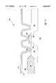
- FIG. 2provides a cross-sectional illustration of a contact produced by depositing a metallization layer in a via and will serve as an example for explaining the term minimum step coverage.
- the substrate 10is covered by a non-conductive passivation layer 12, a diffusion barrier layer 16, and a metallization layer 18.
- the metallization layer 18fails to completely fill the via. Instead, the metallization layer 18 covers the barrier layer 16 but leaves an empty pocket 19 within the via.
- the step coverage for this exampleis found by first dividing a lateral dimension ⁇ (which is the thickness of the metallization layer within the via) by a longitudinal dimension ⁇ (which is the thickness of the metallization layer outside of the via). This factor, ⁇ / ⁇ , is then multiplied by 100 to yield a number which is by definition the step coverage. If the step coverage for the contact is less than the predetermined minimum step coverage, then this contact is defective. That is, the contact will almost certainly fail, even if it conducts initially. This problem is now addressed by using tungsten plugs which conformally deposit in smaller vias at low temperatures.
- the present inventionmeets the aforementioned requirements by providing a process employing a tantalum silicon nitride barrier layer.
- This materialeffectively blocks diffusion between the semiconductor substrate and the metallization layer at significantly higher temperatures than titanium nitride.
- the metallization layercan be deposited at temperatures high enough that the metal conformally fills the vias.
- the inventionproduces stable, uniform contacts in fewer process steps and with fewer pieces of machinery. Specifically, the contacts can be formed without depositing a layer of tungsten. Further, the invention allows formation of ohmic contacts in smaller vias than is permitted with conventional processes.
- Another aspect of the present inventionprovides a method for manufacturing a semiconductor device as described above.
- This methodbegins with a substrate having at least one device element to which electrical contact is to be made, and a non-conductive layer covering the device element. Initially, a via is etched extending through the non-conductive layer thereby exposing a region of the device element found in the substrate. Next, two layers, an ohmic contact layer including tantalum and silicon and a barrier layer including a tantalum silicon nitride, are deposited upon the semiconductor device such that each layer is formed over and in electrical contact with the exposed region of the device element.
- the aforementioned ohmic contact layer, barrier layer, metallization layer, and an additional, anti-reflective, layerare all generated in a single metal deposition system employing the same processing equipment.
- the cycle time for manufacturing the semiconductor deviceis reduced.
- the processing equipmentis less expensive.
- the present inventionis a simple, inexpensive, and effective method of forming ohmic contacts to semiconductor devices.
- FIG. 1is a cross-sectional view of the prior art multi-step contact metallization using a silicide layer, a titanium layer, a tungsten blanket, and multiple titanium nitride layers;
- FIG. 2is a cross-sectional view of a potentially unstable contact of the prior art in which the minimum step coverage is a critical factor;
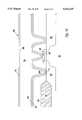
- FIG. 3ais a cross-sectional view of a semiconductor device of the present invention prior to the contact etch
- FIG. 3cis a cross-sectional view of a semiconductor device of the present invention after deposition of the tantalum silicide ohmic contact layer and the tantalum silicon nitride barrier layer prior to metallization;
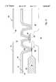
- FIG. 3eis a cross-sectional view of a semiconductor device of another embodiment of the present invention including deposition of a wetting layer.
- the processbegins with a partially fabricated semiconductor device (an MOS device in an integrated circuit in this example) as shown in FIG. 3a.
- the partially fabricated deviceincludes a semiconductor substrate 52 on which are formed a source 58 and a drain 62.
- the region of the semiconductor substrate in which the source and drain are formedis typically lightly doped and known as a well.
- a field oxide layer 56is grown on the substrate 52 to electrically isolate adjacent devices on the integrated circuit.
- the partially fabricated devicealso includes a gate electrode 60 and a gate oxide 59 which are straddled by spacers 61a and 61b.
- FIG. 3cis a cross-sectional view of the semiconductor device of the present invention after a step involving deposition of ohmic contact and barrier layers.
- an ohmic contact layer 70is deposited overlying the exposed region of the source.
- the ohmic contact layer 70includes tantalum and silicon and may form a tantalum silicide having a thickness between about 200-1500 ⁇ , and more preferably between about 500-800 ⁇ .
- a barrier layer 72is deposited overlying the ohmic contact layer 70.
- the barrier layer 72includes a tantalum silicon nitride having a thickness between about 200-1500 ⁇ , and more preferably between about 500-800 ⁇ . Both the ohmic contact layer 70 and the barrier layer 72 are formed over and in electrical contact with the exposed region 66.
- the exact stoichiometry of the ohmic contact and barrier layersmay vary. It appears that suitable layers will have the following stoichiometric ratios: (1) in the range of Ta 74 Si 26 for the ohmic contact layer 70, and (2) in the range of Ta 36 Si 14 N 50 for the barrier layer 72. Particularly preferred barrier layers will have highly amorphous structures.
- FIG. 3dis a cross-sectional view of the semiconductor device of the present invention following the metallization step.
- a metallization layer 74is conformally deposited directly on top of the barrier layer 72. Because the metallization layer must fill the vias (in place of the tungsten plugs employed in conventional processes), it is formed under conditions which completely fill the via and thereby provide good electrical contact with the underlying device component.
- the metallization layer 74includes aluminum or an aluminum alloy (such as those containing copper) and has a thickness between about 0.5-1 microns. Of course, as device sizes shrink, thinner layers may be appropriate.
- the process temperature employed to deposit an aluminum alloy metallization layeris at least about 550° C., and preferably at least about 650° C. Because such temperatures are close to the melting point of aluminum (673° C.), the metallization layer 74 tends to flow somewhat during deposition and, as a result, the device 50 has two important characteristics.
- the metallization layerconformally fills the via 64, thereby producing a stable, uniform contact. More specifically, the via may be as small as 0.2 microns, a fifty percent reduction in size when compared to current manufacturing practices.
- the metallization process for the present inventioncan be performed at even higher temperatures (theoretically up to 900° C.) because the tantalum silicon nitride barrier layer effectively limits diffusion at higher temperatures. This is in contrast to a titanium nitride layer which begins to allow significant diffusion at temperatures of about 650° C.
- FIG. 3eAn alternative embodiment of the present invention is shown in FIG. 3e.
- a "wetting" layer 78is deposited to ensure good contact (i.e., effective wetting) between metallization layer 74 and the walls of the vias.
- wetting layer 78is deposited overlying the barrier layer 72 prior to deposition of the metallization layer 74.
- the wetting layer 78may be necessary in processes where the metal deposition conditions do not ensure that the metallization layer will adequately fill the vias (i.e., where gaps such as those shown in FIG. 2 are a possibility).
Landscapes
- Engineering & Computer Science (AREA)
- Physics & Mathematics (AREA)
- Condensed Matter Physics & Semiconductors (AREA)
- General Physics & Mathematics (AREA)
- Computer Hardware Design (AREA)
- Microelectronics & Electronic Packaging (AREA)
- Power Engineering (AREA)
- Manufacturing & Machinery (AREA)
- Internal Circuitry In Semiconductor Integrated Circuit Devices (AREA)
Abstract
Description
Claims (19)
Priority Applications (2)
| Application Number | Priority Date | Filing Date | Title |
|---|---|---|---|
| US08/378,750US5614437A (en) | 1995-01-26 | 1995-01-26 | Method for fabricating reliable metallization with Ta-Si-N barrier for semiconductors |
| US08/463,064US5525837A (en) | 1995-01-26 | 1995-06-05 | Reliable metallization with barrier for semiconductors |
Applications Claiming Priority (1)
| Application Number | Priority Date | Filing Date | Title |
|---|---|---|---|
| US08/378,750US5614437A (en) | 1995-01-26 | 1995-01-26 | Method for fabricating reliable metallization with Ta-Si-N barrier for semiconductors |
Related Child Applications (1)
| Application Number | Title | Priority Date | Filing Date |
|---|---|---|---|
| US08/463,064DivisionUS5525837A (en) | 1995-01-26 | 1995-06-05 | Reliable metallization with barrier for semiconductors |
Publications (1)
| Publication Number | Publication Date |
|---|---|
| US5614437Atrue US5614437A (en) | 1997-03-25 |
Family
ID=23494400
Family Applications (2)
| Application Number | Title | Priority Date | Filing Date |
|---|---|---|---|
| US08/378,750Expired - LifetimeUS5614437A (en) | 1995-01-26 | 1995-01-26 | Method for fabricating reliable metallization with Ta-Si-N barrier for semiconductors |
| US08/463,064Expired - LifetimeUS5525837A (en) | 1995-01-26 | 1995-06-05 | Reliable metallization with barrier for semiconductors |
Family Applications After (1)
| Application Number | Title | Priority Date | Filing Date |
|---|---|---|---|
| US08/463,064Expired - LifetimeUS5525837A (en) | 1995-01-26 | 1995-06-05 | Reliable metallization with barrier for semiconductors |
Country Status (1)
| Country | Link |
|---|---|
| US (2) | US5614437A (en) |
Cited By (25)
| Publication number | Priority date | Publication date | Assignee | Title |
|---|---|---|---|---|
| US5893752A (en)* | 1997-12-22 | 1999-04-13 | Motorola, Inc. | Process for forming a semiconductor device |
| US5961791A (en)* | 1997-02-26 | 1999-10-05 | Motorola, Inc. | Process for fabricating a semiconductor device |
| US6027998A (en)* | 1997-12-17 | 2000-02-22 | Advanced Micro Devices, Inc. | Method for fully planarized conductive line for a stack gate |
| US6037013A (en)* | 1997-03-06 | 2000-03-14 | Texas Instruments Incorporated | Barrier/liner with a SiNx-enriched surface layer on MOCVD prepared films |
| US6051490A (en)* | 1991-11-29 | 2000-04-18 | Sony Corporation | Method of forming wirings |
| US6090699A (en)* | 1993-10-29 | 2000-07-18 | Kabushiki Kaisha Toshiba | Method of making a semiconductor device |
| US6093966A (en)* | 1998-03-20 | 2000-07-25 | Motorola, Inc. | Semiconductor device with a copper barrier layer and formation thereof |
| US6120915A (en)* | 1997-08-13 | 2000-09-19 | Micron Technology, Inc. | Methods of forming refractory metal silicide components and methods of restricting silicon surface migration of a silicon structure |
| US6313033B1 (en) | 1999-07-27 | 2001-11-06 | Applied Materials, Inc. | Ionized metal plasma Ta, TaNx, W, and WNx liners for gate electrode applications |
| US20010051427A1 (en)* | 1997-08-13 | 2001-12-13 | Yongjun Hu | Methods of forming refractory metal silicide components and methods of restricting silicon surface migration of a silicon structure |
| US6339258B1 (en) | 1999-07-02 | 2002-01-15 | International Business Machines Corporation | Low resistivity tantalum |
| US6365511B1 (en)* | 1999-06-03 | 2002-04-02 | Agere Systems Guardian Corp. | Tungsten silicide nitride as a barrier for high temperature anneals to improve hot carrier reliability |
| US6368969B1 (en) | 2000-06-30 | 2002-04-09 | International Business Machines Corporation | Chemical-mechanical polishing methods |
| US6436825B1 (en) | 2000-04-03 | 2002-08-20 | Taiwan Semiconductor Manufacturing Company | Method of copper barrier layer formation |
| WO2002072002A2 (en) | 2001-03-12 | 2002-09-19 | Biotools Biotechnological & Medical Laboratories, S.A. | Method for preparing stabilised reaction mixtures, which are totally or partially dried, comprising at least one enzyme, reaction mixtures and kits containing said mixtures |
| US6454994B1 (en) | 2000-08-28 | 2002-09-24 | Honeywell International Inc. | Solids comprising tantalum, strontium and silicon |
| US20020192950A1 (en)* | 1999-08-27 | 2002-12-19 | Jiong-Ping Lu | Si-rich surface layer capped diffusion barriers |
| EP1075019A4 (en)* | 1999-02-15 | 2003-01-29 | Asahi Glass Co Ltd | INTEGRATED CIRCUIT DEVICE AND MANUFACTURING METHOD |
| US6566259B1 (en) | 1997-12-02 | 2003-05-20 | Applied Materials, Inc. | Integrated deposition process for copper metallization |
| US6627542B1 (en) | 1999-07-12 | 2003-09-30 | Applied Materials, Inc. | Continuous, non-agglomerated adhesion of a seed layer to a barrier layer |
| US6958290B2 (en) | 2002-05-03 | 2005-10-25 | Texas Instruments Incorporated | Method and apparatus for improving adhesion between layers in integrated devices |
| EP0869544B1 (en)* | 1997-03-31 | 2006-01-11 | Freescale Semiconductor, Inc. | Method for depositing a diffusion barrier |
| US7205665B1 (en)* | 2005-10-03 | 2007-04-17 | Neah Power Systems, Inc. | Porous silicon undercut etching deterrent masks and related methods |
| US7372160B2 (en)* | 2001-05-31 | 2008-05-13 | Stmicroelectronics, Inc. | Barrier film deposition over metal for reduction in metal dishing after CMP |
| US20080138980A1 (en)* | 2006-12-12 | 2008-06-12 | Kyeong-Sik Lee | Method for manufacturing a metal pattern of a semiconductor device |
Families Citing this family (18)
| Publication number | Priority date | Publication date | Assignee | Title |
|---|---|---|---|---|
| JP3294041B2 (en)* | 1994-02-21 | 2002-06-17 | 株式会社東芝 | Semiconductor device |
| US5965942A (en)* | 1994-09-28 | 1999-10-12 | Sharp Kabushiki Kaisha | Semiconductor memory device with amorphous diffusion barrier between capacitor and plug |
| US5962923A (en) | 1995-08-07 | 1999-10-05 | Applied Materials, Inc. | Semiconductor device having a low thermal budget metal filling and planarization of contacts, vias and trenches |
| US5933753A (en)* | 1996-12-16 | 1999-08-03 | International Business Machines Corporation | Open-bottomed via liner structure and method for fabricating same |
| EP0867940A3 (en) | 1997-03-27 | 1999-10-13 | Applied Materials, Inc. | An underlayer for an aluminum interconnect |
| US5895267A (en)* | 1997-07-09 | 1999-04-20 | Lsi Logic Corporation | Method to obtain a low resistivity and conformity chemical vapor deposition titanium film |
| US5882399A (en)* | 1997-08-23 | 1999-03-16 | Applied Materials, Inc. | Method of forming a barrier layer which enables a consistently highly oriented crystalline structure in a metallic interconnect |
| US7253109B2 (en)* | 1997-11-26 | 2007-08-07 | Applied Materials, Inc. | Method of depositing a tantalum nitride/tantalum diffusion barrier layer system |
| US20050272254A1 (en)* | 1997-11-26 | 2005-12-08 | Applied Materials, Inc. | Method of depositing low resistivity barrier layers for copper interconnects |
| WO1999027579A1 (en)* | 1997-11-26 | 1999-06-03 | Applied Materials, Inc. | Damage-free sculptured coating deposition |
| KR100280429B1 (en)* | 1998-01-20 | 2001-02-01 | 김영환 | Layer for preventing diffusion of semiconductor device and fabrication method thereof |
| US6346745B1 (en)* | 1998-12-04 | 2002-02-12 | Advanced Micro Devices, Inc. | Cu-A1 combined interconnect system |
| US6380625B2 (en) | 1999-01-13 | 2002-04-30 | Advanced Micro Devices, Inc. | Semiconductor interconnect barrier and manufacturing method thereof |
| US6413858B1 (en) | 1999-08-27 | 2002-07-02 | Micron Technology, Inc. | Barrier and electroplating seed layer |
| US6555457B1 (en)* | 2000-04-07 | 2003-04-29 | Triquint Technology Holding Co. | Method of forming a laser circuit having low penetration ohmic contact providing impurity gettering and the resultant laser circuit |
| US6294463B1 (en)* | 2000-09-13 | 2001-09-25 | Vanguard International Semiconductor Corp. | Method for manufacturing diffusion barrier layer |
| US6794705B2 (en)* | 2000-12-28 | 2004-09-21 | Infineon Technologies Ag | Multi-layer Pt electrode for DRAM and FRAM with high K dielectric materials |
| US20080124833A1 (en)* | 2006-11-03 | 2008-05-29 | International Business Machines Corporation | Method for filling holes with metal chalcogenide material |
Citations (19)
| Publication number | Priority date | Publication date | Assignee | Title |
|---|---|---|---|---|
| US4502209A (en)* | 1983-08-31 | 1985-03-05 | At&T Bell Laboratories | Forming low-resistance contact to silicon |
| US4640004A (en)* | 1984-04-13 | 1987-02-03 | Fairchild Camera & Instrument Corp. | Method and structure for inhibiting dopant out-diffusion |
| US4782380A (en)* | 1987-01-22 | 1988-11-01 | Advanced Micro Devices, Inc. | Multilayer interconnection for integrated circuit structure having two or more conductive metal layers |
| US4804636A (en)* | 1985-05-01 | 1989-02-14 | Texas Instruments Incorporated | Process for making integrated circuits having titanium nitride triple interconnect |
| US4888297A (en)* | 1982-09-20 | 1989-12-19 | International Business Machines Corporation | Process for making a contact structure including polysilicon and metal alloys |
| US4912543A (en)* | 1983-07-20 | 1990-03-27 | Siemens Aktiengesellschaft | Integrated semiconductor circuit having an external contacting track level consisting of aluminum or of an aluminum alloy |
| US4981550A (en)* | 1987-09-25 | 1991-01-01 | At&T Bell Laboratories | Semiconductor device having tungsten plugs |
| US5066615A (en)* | 1989-10-23 | 1991-11-19 | At&T Bell Laboratories | Photolithographic processes using thin coatings of refractory metal silicon nitrides as antireflection layers |
| US5135878A (en)* | 1990-08-28 | 1992-08-04 | Solid State Devices, Inc. | Schottky diode |
| US5142438A (en)* | 1991-11-15 | 1992-08-25 | Micron Technology, Inc. | Dram cell having a stacked capacitor with a tantalum lower plate, a tantalum oxide dielectric layer, and a silicide buried contact |
| US5231055A (en)* | 1989-01-13 | 1993-07-27 | Texas Instruments Incorporated | Method of forming composite interconnect system |
| US5240880A (en)* | 1992-05-05 | 1993-08-31 | Zilog, Inc. | Ti/TiN/Ti contact metallization |
| US5275715A (en)* | 1992-01-23 | 1994-01-04 | Micron Technology Inc. | Electroplating process for enhancing the conformality of titanium and titanium nitride films in the manufacture of integrated circuits and structures produced thereby |
| US5278099A (en)* | 1985-05-13 | 1994-01-11 | Kabushiki Kaisha Toshiba | Method for manufacturing a semiconductor device having wiring electrodes |
| US5281838A (en)* | 1990-03-13 | 1994-01-25 | Mitsubishi Denki Kabushiki Kaisha | Semiconductor device having contact between wiring layer and impurity region |
| US5312772A (en)* | 1988-08-06 | 1994-05-17 | Seiko Epson Corporation | Method of manufacturing interconnect metallization comprising metal nitride and silicide |
| US5341016A (en)* | 1993-06-16 | 1994-08-23 | Micron Semiconductor, Inc. | Low resistance device element and interconnection structure |
| US5489548A (en)* | 1994-08-01 | 1996-02-06 | Texas Instruments Incorporated | Method of forming high-dielectric-constant material electrodes comprising sidewall spacers |
| US5504041A (en)* | 1994-08-01 | 1996-04-02 | Texas Instruments Incorporated | Conductive exotic-nitride barrier layer for high-dielectric-constant materials |
Family Cites Families (3)
| Publication number | Priority date | Publication date | Assignee | Title |
|---|---|---|---|---|
| JPS6373660A (en)* | 1986-09-17 | 1988-04-04 | Fujitsu Ltd | Semiconductor device |
| US4926237A (en)* | 1988-04-04 | 1990-05-15 | Motorola, Inc. | Device metallization, device and method |
| JPH0795539B2 (en)* | 1989-12-04 | 1995-10-11 | 日鉄セミコンダクター株式会社 | Integrated circuit and manufacturing method thereof |
- 1995
- 1995-01-26USUS08/378,750patent/US5614437A/ennot_activeExpired - Lifetime
- 1995-06-05USUS08/463,064patent/US5525837A/ennot_activeExpired - Lifetime
Patent Citations (19)
| Publication number | Priority date | Publication date | Assignee | Title |
|---|---|---|---|---|
| US4888297A (en)* | 1982-09-20 | 1989-12-19 | International Business Machines Corporation | Process for making a contact structure including polysilicon and metal alloys |
| US4912543A (en)* | 1983-07-20 | 1990-03-27 | Siemens Aktiengesellschaft | Integrated semiconductor circuit having an external contacting track level consisting of aluminum or of an aluminum alloy |
| US4502209A (en)* | 1983-08-31 | 1985-03-05 | At&T Bell Laboratories | Forming low-resistance contact to silicon |
| US4640004A (en)* | 1984-04-13 | 1987-02-03 | Fairchild Camera & Instrument Corp. | Method and structure for inhibiting dopant out-diffusion |
| US4804636A (en)* | 1985-05-01 | 1989-02-14 | Texas Instruments Incorporated | Process for making integrated circuits having titanium nitride triple interconnect |
| US5278099A (en)* | 1985-05-13 | 1994-01-11 | Kabushiki Kaisha Toshiba | Method for manufacturing a semiconductor device having wiring electrodes |
| US4782380A (en)* | 1987-01-22 | 1988-11-01 | Advanced Micro Devices, Inc. | Multilayer interconnection for integrated circuit structure having two or more conductive metal layers |
| US4981550A (en)* | 1987-09-25 | 1991-01-01 | At&T Bell Laboratories | Semiconductor device having tungsten plugs |
| US5312772A (en)* | 1988-08-06 | 1994-05-17 | Seiko Epson Corporation | Method of manufacturing interconnect metallization comprising metal nitride and silicide |
| US5231055A (en)* | 1989-01-13 | 1993-07-27 | Texas Instruments Incorporated | Method of forming composite interconnect system |
| US5066615A (en)* | 1989-10-23 | 1991-11-19 | At&T Bell Laboratories | Photolithographic processes using thin coatings of refractory metal silicon nitrides as antireflection layers |
| US5281838A (en)* | 1990-03-13 | 1994-01-25 | Mitsubishi Denki Kabushiki Kaisha | Semiconductor device having contact between wiring layer and impurity region |
| US5135878A (en)* | 1990-08-28 | 1992-08-04 | Solid State Devices, Inc. | Schottky diode |
| US5142438A (en)* | 1991-11-15 | 1992-08-25 | Micron Technology, Inc. | Dram cell having a stacked capacitor with a tantalum lower plate, a tantalum oxide dielectric layer, and a silicide buried contact |
| US5275715A (en)* | 1992-01-23 | 1994-01-04 | Micron Technology Inc. | Electroplating process for enhancing the conformality of titanium and titanium nitride films in the manufacture of integrated circuits and structures produced thereby |
| US5240880A (en)* | 1992-05-05 | 1993-08-31 | Zilog, Inc. | Ti/TiN/Ti contact metallization |
| US5341016A (en)* | 1993-06-16 | 1994-08-23 | Micron Semiconductor, Inc. | Low resistance device element and interconnection structure |
| US5489548A (en)* | 1994-08-01 | 1996-02-06 | Texas Instruments Incorporated | Method of forming high-dielectric-constant material electrodes comprising sidewall spacers |
| US5504041A (en)* | 1994-08-01 | 1996-04-02 | Texas Instruments Incorporated | Conductive exotic-nitride barrier layer for high-dielectric-constant materials |
Non-Patent Citations (10)
| Title |
|---|
| Kolawa, E., Molarius, a ) C.W. Nieh, M. A. Nicolet, Amorphous Ta Si N thin film alloys as diffusion barrier in Al/Si metallizations; pp. 3006 3010, J. Vac. Sci. Technol. A8 (3); American Vacuum Society; May/Jun. 1990.* |
| Kolawa, E., Molarius, a) C.W. Nieh, M.-A. Nicolet, "Amorphous Ta-Si-N thin-film alloys as diffusion barrier in Al/Si metallizations;" pp. 3006-3010, J. Vac. Sci. Technol. A8 (3); American Vacuum Society; May/Jun. 1990. |
| Kolawa, Elzbieta; Halperin, Louis W., Vu, Quat; Nicolet, Marc A; Amorphous Ternary Thin Film Alloys as Diffusion Barriers in Silicon Metallizations, pp. 243 247; California Institute of Technology; 1990.* |
| Kolawa, Elzbieta; Halperin, Louis W., Vu, Quat; Nicolet, Marc-A; "Amorphous Ternary Thin-Film Alloys as Diffusion Barriers in Silicon Metallizations," pp. 243-247; California Institute of Technology; 1990. |
| Kwok, C. K., Kolawa, E., Nicolet, M A., Lee, Ray L.; Stress and Resistivity in Reactively Supttered Amorphous Metallic Ta Si N Films ; California Institute of Technology.* |
| Kwok, C.-K., Kolawa, E., Nicolet, M-A., Lee, Ray L.; "Stress and Resistivity in Reactively Supttered Amorphous Metallic Ta-Si-N Films"; California Institute of Technology. |
| Wolf et al., Silicon Processing for the VLSI Era, vol. I, Lattice Press, 1986, pp. 384 400.* |
| Wolf et al., Silicon Processing for the VLSI Era, vol. I, Lattice Press, 1986, pp. 384-400. |
| Wolf et al., Silicon Processing for the VLSI Era, vol. II, Lattice Press, 1990, pp. 132 133.* |
| Wolf et al., Silicon Processing for the VLSI Era, vol. II, Lattice Press, 1990, pp. 132-133. |
Cited By (36)
| Publication number | Priority date | Publication date | Assignee | Title |
|---|---|---|---|---|
| US6051490A (en)* | 1991-11-29 | 2000-04-18 | Sony Corporation | Method of forming wirings |
| US6794286B2 (en)* | 1993-10-29 | 2004-09-21 | Kabushiki Kaisha Toshiba | Process for fabricating a metal wiring and metal contact in a semicondutor device |
| US6090699A (en)* | 1993-10-29 | 2000-07-18 | Kabushiki Kaisha Toshiba | Method of making a semiconductor device |
| US5961791A (en)* | 1997-02-26 | 1999-10-05 | Motorola, Inc. | Process for fabricating a semiconductor device |
| US6037013A (en)* | 1997-03-06 | 2000-03-14 | Texas Instruments Incorporated | Barrier/liner with a SiNx-enriched surface layer on MOCVD prepared films |
| EP0869544B1 (en)* | 1997-03-31 | 2006-01-11 | Freescale Semiconductor, Inc. | Method for depositing a diffusion barrier |
| US20010051427A1 (en)* | 1997-08-13 | 2001-12-13 | Yongjun Hu | Methods of forming refractory metal silicide components and methods of restricting silicon surface migration of a silicon structure |
| US6127270A (en)* | 1997-08-13 | 2000-10-03 | Micron Technology, Inc. | Methods of forming refractory metal silicide components and methods of restricting silicon surface migration of a silicon structure |
| US20040132286A9 (en)* | 1997-08-13 | 2004-07-08 | Yongjun Hu | Methods of forming refractory metal silicide components and methods of restricting silicon surface migration of a silicon structure |
| US6468905B1 (en) | 1997-08-13 | 2002-10-22 | Micron Technology, Inc. | Methods of restricting silicon migration |
| US6120915A (en)* | 1997-08-13 | 2000-09-19 | Micron Technology, Inc. | Methods of forming refractory metal silicide components and methods of restricting silicon surface migration of a silicon structure |
| US6953749B2 (en) | 1997-08-13 | 2005-10-11 | Micron Technology, Inc. | Methods of forming refractory metal silicide components and methods of restricting silicon surface migration of a silicon structure |
| US6881673B2 (en) | 1997-12-02 | 2005-04-19 | Applied Materials, Inc. | Integrated deposition process for copper metallization |
| US6566259B1 (en) | 1997-12-02 | 2003-05-20 | Applied Materials, Inc. | Integrated deposition process for copper metallization |
| US20030194863A1 (en)* | 1997-12-02 | 2003-10-16 | Applied Materials, Inc. | Integrated deposition process for copper metallization |
| US6027998A (en)* | 1997-12-17 | 2000-02-22 | Advanced Micro Devices, Inc. | Method for fully planarized conductive line for a stack gate |
| US5893752A (en)* | 1997-12-22 | 1999-04-13 | Motorola, Inc. | Process for forming a semiconductor device |
| US6093966A (en)* | 1998-03-20 | 2000-07-25 | Motorola, Inc. | Semiconductor device with a copper barrier layer and formation thereof |
| EP1075019A4 (en)* | 1999-02-15 | 2003-01-29 | Asahi Glass Co Ltd | INTEGRATED CIRCUIT DEVICE AND MANUFACTURING METHOD |
| US6365511B1 (en)* | 1999-06-03 | 2002-04-02 | Agere Systems Guardian Corp. | Tungsten silicide nitride as a barrier for high temperature anneals to improve hot carrier reliability |
| US6339258B1 (en) | 1999-07-02 | 2002-01-15 | International Business Machines Corporation | Low resistivity tantalum |
| US6627542B1 (en) | 1999-07-12 | 2003-09-30 | Applied Materials, Inc. | Continuous, non-agglomerated adhesion of a seed layer to a barrier layer |
| US6313033B1 (en) | 1999-07-27 | 2001-11-06 | Applied Materials, Inc. | Ionized metal plasma Ta, TaNx, W, and WNx liners for gate electrode applications |
| US20020192950A1 (en)* | 1999-08-27 | 2002-12-19 | Jiong-Ping Lu | Si-rich surface layer capped diffusion barriers |
| US6680249B2 (en)* | 1999-08-27 | 2004-01-20 | Texas Instruments Incorporated | Si-rich surface layer capped diffusion barriers |
| US6436825B1 (en) | 2000-04-03 | 2002-08-20 | Taiwan Semiconductor Manufacturing Company | Method of copper barrier layer formation |
| US6368969B1 (en) | 2000-06-30 | 2002-04-09 | International Business Machines Corporation | Chemical-mechanical polishing methods |
| US6454994B1 (en) | 2000-08-28 | 2002-09-24 | Honeywell International Inc. | Solids comprising tantalum, strontium and silicon |
| WO2002072002A2 (en) | 2001-03-12 | 2002-09-19 | Biotools Biotechnological & Medical Laboratories, S.A. | Method for preparing stabilised reaction mixtures, which are totally or partially dried, comprising at least one enzyme, reaction mixtures and kits containing said mixtures |
| US7372160B2 (en)* | 2001-05-31 | 2008-05-13 | Stmicroelectronics, Inc. | Barrier film deposition over metal for reduction in metal dishing after CMP |
| US20080188077A1 (en)* | 2001-05-31 | 2008-08-07 | Stmicroelectronics, Inc. | Barrier film deposition over metal for reduction in metal dishing after CMP |
| US7534719B2 (en) | 2001-05-31 | 2009-05-19 | Stmicroelectronics, Inc. | Method for reduction in metal dishing after CMP |
| US6958290B2 (en) | 2002-05-03 | 2005-10-25 | Texas Instruments Incorporated | Method and apparatus for improving adhesion between layers in integrated devices |
| US7205665B1 (en)* | 2005-10-03 | 2007-04-17 | Neah Power Systems, Inc. | Porous silicon undercut etching deterrent masks and related methods |
| US20070090530A1 (en)* | 2005-10-03 | 2007-04-26 | Vinh Chung | Porous silicon undercut etching deterrent masks and related methods |
| US20080138980A1 (en)* | 2006-12-12 | 2008-06-12 | Kyeong-Sik Lee | Method for manufacturing a metal pattern of a semiconductor device |
Also Published As
| Publication number | Publication date |
|---|---|
| US5525837A (en) | 1996-06-11 |
Similar Documents
| Publication | Publication Date | Title |
|---|---|---|
| US5614437A (en) | Method for fabricating reliable metallization with Ta-Si-N barrier for semiconductors | |
| US6015749A (en) | Method to improve adhesion between copper and titanium nitride, for copper interconnect structures, via the use of an ion implantation procedure | |
| US5674781A (en) | Landing pad technology doubled up as a local interconnect and borderless contact for deep sub-half micrometer IC application | |
| US6124203A (en) | Method for forming conformal barrier layers | |
| EP0506426B1 (en) | Integrated circuit metallization with zero contact enclosure requirements and method of making the same | |
| US6913997B2 (en) | Method of using tantalum-aluminum-nitrogen material as diffusion barrier and adhesion layer in semiconductor devices | |
| US20100230815A1 (en) | Semiconductor device | |
| US7186642B2 (en) | Low temperature nitride used as Cu barrier layer | |
| US20070197015A1 (en) | Methods for forming a metal contact in a semiconductor device in which an ohmic layer is formed while forming a barrier metal layer | |
| US7635644B2 (en) | Semiconductor device including metal interconnection and method for forming metal interconnection | |
| US6362526B1 (en) | Alloy barrier layers for semiconductors | |
| US6849541B1 (en) | Method of fabricating a dual damascene copper wire | |
| US5950108A (en) | Method of fabricating a conductive plug | |
| US5625231A (en) | Low cost solution to high aspect ratio contact/via adhesion layer application for deep sub-half micrometer back-end-of line technology | |
| US6150268A (en) | Barrier materials for metal interconnect | |
| US9812391B2 (en) | Advanced metallization for damage repair | |
| US6239015B1 (en) | Semiconductor device having polysilicon interconnections and method of making same | |
| US7875978B2 (en) | Metal line having a multi-layered diffusion layer in a semiconductor device and method for forming the same | |
| KR100373193B1 (en) | Method for the fabrication of contacts in an integrated circuit device | |
| KR100197992B1 (en) | Metal wiring formation method of semiconductor device | |
| KR20020027996A (en) | method for manufacturing of semiconductor device | |
| JPH10135326A (en) | BPSG reflow and method for suppressing pattern distortion associated with integrated circuit chips formed thereby | |
| KR20020052566A (en) | Method of fabricating conductive lines and interconnections in semiconductor devices | |
| KR19980047201A (en) | Wiring Formation Method | |
| KR20000041322A (en) | Via contact forming method of semiconductor device |
Legal Events
| Date | Code | Title | Description |
|---|---|---|---|
| AS | Assignment | Owner name:LSI LOGIC CORPORATION, CALIFORNIA Free format text:ASSIGNMENT OF ASSIGNORS INTEREST;ASSIGNOR:CHOUDHURY, RATAN K.;REEL/FRAME:007348/0380 Effective date:19950125 | |
| STCF | Information on status: patent grant | Free format text:PATENTED CASE | |
| FEPP | Fee payment procedure | Free format text:PAYOR NUMBER ASSIGNED (ORIGINAL EVENT CODE: ASPN); ENTITY STATUS OF PATENT OWNER: LARGE ENTITY | |
| FPAY | Fee payment | Year of fee payment:4 | |
| REMI | Maintenance fee reminder mailed | ||
| FPAY | Fee payment | Year of fee payment:8 | |
| SULP | Surcharge for late payment | Year of fee payment:7 | |
| FEPP | Fee payment procedure | Free format text:PAYER NUMBER DE-ASSIGNED (ORIGINAL EVENT CODE: RMPN); ENTITY STATUS OF PATENT OWNER: LARGE ENTITY Free format text:PAYOR NUMBER ASSIGNED (ORIGINAL EVENT CODE: ASPN); ENTITY STATUS OF PATENT OWNER: LARGE ENTITY | |
| FPAY | Fee payment | Year of fee payment:12 | |
| AS | Assignment | Owner name:DEUTSCHE BANK AG NEW YORK BRANCH, AS COLLATERAL AG Free format text:PATENT SECURITY AGREEMENT;ASSIGNORS:LSI CORPORATION;AGERE SYSTEMS LLC;REEL/FRAME:032856/0031 Effective date:20140506 | |
| AS | Assignment | Owner name:LSI CORPORATION, CALIFORNIA Free format text:CHANGE OF NAME;ASSIGNOR:LSI LOGIC CORPORATION;REEL/FRAME:033102/0270 Effective date:20070406 | |
| AS | Assignment | Owner name:AVAGO TECHNOLOGIES GENERAL IP (SINGAPORE) PTE. LTD Free format text:ASSIGNMENT OF ASSIGNORS INTEREST;ASSIGNOR:LSI CORPORATION;REEL/FRAME:035390/0388 Effective date:20140814 | |
| AS | Assignment | Owner name:AGERE SYSTEMS LLC, PENNSYLVANIA Free format text:TERMINATION AND RELEASE OF SECURITY INTEREST IN PATENT RIGHTS (RELEASES RF 032856-0031);ASSIGNOR:DEUTSCHE BANK AG NEW YORK BRANCH, AS COLLATERAL AGENT;REEL/FRAME:037684/0039 Effective date:20160201 Owner name:LSI CORPORATION, CALIFORNIA Free format text:TERMINATION AND RELEASE OF SECURITY INTEREST IN PATENT RIGHTS (RELEASES RF 032856-0031);ASSIGNOR:DEUTSCHE BANK AG NEW YORK BRANCH, AS COLLATERAL AGENT;REEL/FRAME:037684/0039 Effective date:20160201 | |
| AS | Assignment | Owner name:BELL SEMICONDUCTOR, LLC, ILLINOIS Free format text:ASSIGNMENT OF ASSIGNORS INTEREST;ASSIGNORS:AVAGO TECHNOLOGIES GENERAL IP (SINGAPORE) PTE. LTD.;BROADCOM CORPORATION;REEL/FRAME:044886/0608 Effective date:20171208 | |
| AS | Assignment | Owner name:CORTLAND CAPITAL MARKET SERVICES LLC, AS COLLATERA Free format text:SECURITY INTEREST;ASSIGNORS:HILCO PATENT ACQUISITION 56, LLC;BELL SEMICONDUCTOR, LLC;BELL NORTHERN RESEARCH, LLC;REEL/FRAME:045216/0020 Effective date:20180124 | |
| AS | Assignment | Owner name:BELL NORTHERN RESEARCH, LLC, ILLINOIS Free format text:RELEASE BY SECURED PARTY;ASSIGNOR:CORTLAND CAPITAL MARKET SERVICES LLC;REEL/FRAME:059720/0719 Effective date:20220401 Owner name:BELL SEMICONDUCTOR, LLC, ILLINOIS Free format text:RELEASE BY SECURED PARTY;ASSIGNOR:CORTLAND CAPITAL MARKET SERVICES LLC;REEL/FRAME:059720/0719 Effective date:20220401 Owner name:HILCO PATENT ACQUISITION 56, LLC, ILLINOIS Free format text:RELEASE BY SECURED PARTY;ASSIGNOR:CORTLAND CAPITAL MARKET SERVICES LLC;REEL/FRAME:059720/0719 Effective date:20220401 |