US5613293A - Method of making a smooth topography head/disk interface surface on a head with patterned pole - Google Patents
Method of making a smooth topography head/disk interface surface on a head with patterned poleDownload PDFInfo
- Publication number
- US5613293A US5613293AUS08/476,899US47689995AUS5613293AUS 5613293 AUS5613293 AUS 5613293AUS 47689995 AUS47689995 AUS 47689995AUS 5613293 AUS5613293 AUS 5613293A
- Authority
- US
- United States
- Prior art keywords
- photoresist
- working surface
- thin
- fill material
- head
- Prior art date
- Legal status (The legal status is an assumption and is not a legal conclusion. Google has not performed a legal analysis and makes no representation as to the accuracy of the status listed.)
- Expired - Lifetime
Links
Images


Classifications
- G—PHYSICS
- G11—INFORMATION STORAGE
- G11B—INFORMATION STORAGE BASED ON RELATIVE MOVEMENT BETWEEN RECORD CARRIER AND TRANSDUCER
- G11B5/00—Recording by magnetisation or demagnetisation of a record carrier; Reproducing by magnetic means; Record carriers therefor
- G11B5/127—Structure or manufacture of heads, e.g. inductive
- G11B5/31—Structure or manufacture of heads, e.g. inductive using thin films
- G11B5/3163—Fabrication methods or processes specially adapted for a particular head structure, e.g. using base layers for electroplating, using functional layers for masking, using energy or particle beams for shaping the structure or modifying the properties of the basic layers
- G—PHYSICS
- G11—INFORMATION STORAGE
- G11B—INFORMATION STORAGE BASED ON RELATIVE MOVEMENT BETWEEN RECORD CARRIER AND TRANSDUCER
- G11B5/00—Recording by magnetisation or demagnetisation of a record carrier; Reproducing by magnetic means; Record carriers therefor
- G11B5/127—Structure or manufacture of heads, e.g. inductive
- G11B5/31—Structure or manufacture of heads, e.g. inductive using thin films
- G11B5/3103—Structure or manufacture of integrated heads or heads mechanically assembled and electrically connected to a support or housing
- G11B5/3106—Structure or manufacture of integrated heads or heads mechanically assembled and electrically connected to a support or housing where the integrated or assembled structure comprises means for conditioning against physical detrimental influence, e.g. wear, contamination
- G—PHYSICS
- G11—INFORMATION STORAGE
- G11B—INFORMATION STORAGE BASED ON RELATIVE MOVEMENT BETWEEN RECORD CARRIER AND TRANSDUCER
- G11B5/00—Recording by magnetisation or demagnetisation of a record carrier; Reproducing by magnetic means; Record carriers therefor
- G11B5/127—Structure or manufacture of heads, e.g. inductive
- G11B5/31—Structure or manufacture of heads, e.g. inductive using thin films
- G11B5/3109—Details
- G11B5/3116—Shaping of layers, poles or gaps for improving the form of the electrical signal transduced, e.g. for shielding, contour effect, equalizing, side flux fringing, cross talk reduction between heads or between heads and information tracks
- G—PHYSICS
- G11—INFORMATION STORAGE
- G11B—INFORMATION STORAGE BASED ON RELATIVE MOVEMENT BETWEEN RECORD CARRIER AND TRANSDUCER
- G11B5/00—Recording by magnetisation or demagnetisation of a record carrier; Reproducing by magnetic means; Record carriers therefor
- G11B5/127—Structure or manufacture of heads, e.g. inductive
- G11B5/33—Structure or manufacture of flux-sensitive heads, i.e. for reproduction only; Combination of such heads with means for recording or erasing only
- G11B5/39—Structure or manufacture of flux-sensitive heads, i.e. for reproduction only; Combination of such heads with means for recording or erasing only using magneto-resistive devices or effects
- G11B5/3903—Structure or manufacture of flux-sensitive heads, i.e. for reproduction only; Combination of such heads with means for recording or erasing only using magneto-resistive devices or effects using magnetic thin film layers or their effects, the films being part of integrated structures
- G11B5/3967—Composite structural arrangements of transducers, e.g. inductive write and magnetoresistive read
- Y—GENERAL TAGGING OF NEW TECHNOLOGICAL DEVELOPMENTS; GENERAL TAGGING OF CROSS-SECTIONAL TECHNOLOGIES SPANNING OVER SEVERAL SECTIONS OF THE IPC; TECHNICAL SUBJECTS COVERED BY FORMER USPC CROSS-REFERENCE ART COLLECTIONS [XRACs] AND DIGESTS
- Y10—TECHNICAL SUBJECTS COVERED BY FORMER USPC
- Y10T—TECHNICAL SUBJECTS COVERED BY FORMER US CLASSIFICATION
- Y10T29/00—Metal working
- Y10T29/49—Method of mechanical manufacture
- Y10T29/49002—Electrical device making
- Y10T29/4902—Electromagnet, transformer or inductor
- Y10T29/49021—Magnetic recording reproducing transducer [e.g., tape head, core, etc.]
- Y10T29/49032—Fabricating head structure or component thereof
- Y10T29/49036—Fabricating head structure or component thereof including measuring or testing
- Y10T29/49041—Fabricating head structure or component thereof including measuring or testing with significant slider/housing shaping or treating
- Y—GENERAL TAGGING OF NEW TECHNOLOGICAL DEVELOPMENTS; GENERAL TAGGING OF CROSS-SECTIONAL TECHNOLOGIES SPANNING OVER SEVERAL SECTIONS OF THE IPC; TECHNICAL SUBJECTS COVERED BY FORMER USPC CROSS-REFERENCE ART COLLECTIONS [XRACs] AND DIGESTS
- Y10—TECHNICAL SUBJECTS COVERED BY FORMER USPC
- Y10T—TECHNICAL SUBJECTS COVERED BY FORMER US CLASSIFICATION
- Y10T29/00—Metal working
- Y10T29/49—Method of mechanical manufacture
- Y10T29/49002—Electrical device making
- Y10T29/4902—Electromagnet, transformer or inductor
- Y10T29/49021—Magnetic recording reproducing transducer [e.g., tape head, core, etc.]
- Y10T29/49032—Fabricating head structure or component thereof
- Y10T29/49036—Fabricating head structure or component thereof including measuring or testing
- Y10T29/49043—Depositing magnetic layer or coating
- Y10T29/49046—Depositing magnetic layer or coating with etching or machining of magnetic material
Definitions
- the present inventionrelates to the surface of a thin-film magnetic head serving as the interface between the head and a recording medium. More particularly, it relates to a thin-film head with a smooth topography interface surface which has patterned magnetic poles.
- thin-film magnetic headsretrieve (“read”) and store (“write”) information to magnetic media by magneto-resistively or inductively sensing the magnetization of and creating respectively, localized magnetic domains in the media.
- a thin-film head's interface surfacemoves over the medium at a short distance from the medium so that magnetic flux from the localized domains enters permeable material pole tips in the interface surface.
- This fluxextends over a selected permeable material path from the surface of the pole tips at the interface surface to an electromagnetic transducer which converts the magnetic flux in the path into an electric read current.
- the electric read currentis used by the recording device in which the head is mounted to create an electric read signal.
- Thin-film headsare usually constructed using material deposition and etching techniques similar to those used in monolithic integrated circuit construction.
- large numbers of headsare constructed on a large substrate, usually a wafer, by material deposition and etching techniques which construct the thin-film heads by layers.
- the headsare built up in a direction parallel to the plane of the eventual interface surface which is perpendicular to the plane of the substrate surface. This means that the basis for the eventual interface surface is located within the wafer when the deposition and etching process on the wafer is finished.
- the waferis sliced into rows near the ends of the pole tips. For each thin-film head, this creates a working surface that includes the surfaces of the pole tips.
- the individual thin-film headsare simply cut from these rows and placed, as is, into magnetic recording devices with the working surfaces serving as the interface surfaces.
- the shape of the pole tipsis determined by the wafer-level etching and deposition procedures.
- the ends of the pole tips near the working surfaceare reshaped after the thin-film heads are cut into rows.
- the rows of thin-film headsare rotated to place the working surfaces in a common plane.
- Portions of the working surfacesare then masked with a layer of photoresist using known photoresist technology.
- a removal agentsuch as an etching substance or ion milling beam, is then directed towards the masked and unmasked portions of the working surfaces. The removal agent removes material from the unmasked portions without affecting the masked portions, creating a depression around the masked portions and reshaping the ends of the pole tips near the pole tip surfaces.
- the present inventionis a thin-film head with patterned poles and a smooth interface surface topography.
- the polesare patterned after the wafer has been cut into rows by etching around a masked portion of the pole tips.
- the depression in the interface surface created by this etchingis removed by depositing a fill material over the entire interface surface. This fill material is then selectively removed until the pole tips are once again exposed and the interface surface has a smooth topography.
- the pole tipsare masked with a photoresist which bonds to the areas of the interface surface which are to remain intact through the etching process. After the etching or milling is finished, the photoresist is not removed. Instead, fill material is deposited directly over both the areas covered by the photoresist and the areas not covered by the photoresist.
- the fill material on top of the photoresistis removed by either a purely mechanical process or the combination of a mechanical process and a heating process involving a laser beam.
- the fill materialis repeatedly struck causing the photoresist to fracture from the interface surface. This fracturing causes the photoresist and the fill material covering the photoresist to break off from the interface surface.
- a laserheats the photoresist indirectly by heating the fill material. The heat causes the photoresist to craze and the small cracks formed in the photoresist when it crazes reduce the strength of its bond to the interface surface.
- a low intensity mechanical processthen fractures the photoresist from the pole tip surface causing the photoresist and the fill material covering it to fall away from the pole tips.
- the fill material which does not cover the photoresistis reduced to the level of the shaped pole tips by lapping the fill material.
- the lapped materialcreates a smooth topography with the pole tip surfaces and thus removes the depressions around the pole tips which accumulate foreign material.
- the present inventioncreates a smooth topography interface surface with patterned poles.
- This smooth topographyeliminates depressions in the interface surface which can accumulate foreign material. Because it does not accumulate foreign material, the thin-film head of the present invention suffers from less mechanical damage than many thin-film heads of the past.
- FIG. 1is a portion of a wafer of partially constructed thin-film heads
- FIG. 2is a cross-sectional side view of an inductive partially constructed thin-film head
- FIG. 3Ais an isometric view of the working surface of a partially constructed thin-film head after being cut from the wafer of FIG. 1;
- FIG. 3Bis an isometric view of the partially constructed thin-film head of FIG. 3A with a film of photoresist applied to the working surface;
- FIG. 3Cis an isometric view of the partially constructed thin-film head with the unmasked portions of the photoresist removed;
- FIG. 3Dis an isometric view of the partially constructed thin-film head after unmasked material has been removed
- FIG. 3Eis an isometric view of the partially constructed thin-film head after fill material has been added to the depression
- FIG. 3Fis an isometric view of the partially constructed thin-film head after the photoresist of the masked portions has been removed.
- FIG. 3Gis an isometric view of the thin-film head after the fill material has been lapped so that it is level with the shaped pole tips.
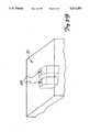
- FIG. 1is a portion of a wafer 20 containing a plurality of partially constructed inductive thin-film heads 22 formed through appropriate material depositions and etchings on a substrate 24 in a well known manner. To avoid obscuring the view of the remainder of the heads, FIG. 1 does not show a final insulation layer which lies over the top of thin-film heads 22. Thin-film heads 22 are constructed in rows and are cut from wafer 20 along cut lines 26 which intersect top pole tips 28 and bottom pole tips 30 (not shown).
- FIG. 2is a cross-sectional side view of an inductive thin-film head 22 broken away from wafer 20.
- Working surface 50 shown on the right side of thin-film inductive head 22,is the surface produced by cut lines 26 of FIG. 1.
- Thin-film head 22is constructed in wafer 20 by depositing and etching layers of material onto substrate 24.
- a bottom insulating layer 32 of nonmagnetic materialsuch as Al 2 O 3 is first deposited on substrate 24.
- a bottom core leg 34 forming a bottom pole tip 30 near working surface 50is deposited on top of bottom insulating layer 32.
- a top core leg 38is formed above bottom core leg 34 and forms top pole tip 28 near working surface 50.
- the two core legsare typically constructed out of a nickel-iron alloy chosen for its magnetic properties.
- top core leg 38 and bottom core leg 34Between top core leg 38 and bottom core leg 34 is an insulating material 42 which houses conductive coils 44 and 46. Top pole tip 28 and bottom pole tip 30 form a gap 48 between them which is typically filled with a nonmagnetic material such as Al 2 O 3 . Above top core leg 38 is top insulating layer 52 which is also preferably Al 2 O 3 . Cut line 26 cuts through top insulating layer 52, top pole tip 28, gap 48, bottom pole tip 30 and bottom insulating layer 32 to form working surface 50 which is perpendicular to the plane of substrate 24.
- working surface 50is placed proximate to a magnetic media containing localized magnetic domains.
- magnetic flux from the domainsextends through top core leg 38 and bottom core leg 34.
- an inductive headsuch as the one shown in FIG. 2
- the changing magnetic fluxinduces current to flow through conductive coils 44 and 46.
- the direction of the current flowis indicative of the direction of the magnetic fields of the localized domains.
- the current through conductive coils 44 and 46represents the magnetic signal stored as the magnetization of the magnetic medium's local domains.
- an inductive headis shown in FIG. 2, those skilled in the art will recognize that the smooth topography interface surface with patterned poles described below may be used with other types of heads including magneto-resistive heads.
- FIG. 3Ais an isometric view of working surface 50 just after partially constructed thin-film head 22 has been cut from wafer 20 along cut line 26 of FIG. 1. Portions of bottom pole tip 30 and top pole tip 28 below working surface 50 are shown in dashed line form while the cross-sectional surfaces of the pole tips at working surface 50 are shown in solid line form. Pole tips 28 and 30 have a cross-sectional trapezoidal shape resulting from the material depositions and etchings performed to construct thin-film head 22 on top of substrate 24. Bottom insulating layer 32, gap 48 and top insulating layer 52 are typically constructed of the same nonmagnetic material. Together, they surround pole tips 28 and 30 at working surface 50 to form an integral unit.
- the rows of thin-film headsare broken off wafer 20 and rotated to substantially place all of the working surfaces 50 of all the rows in a common plane.
- the rotated rowsare then composed into a single unit by means of an adhesive which allows further deposition and etching techniques to be performed in a batch process at or near working surfaces 50 to reshape the ends of top pole tip 28 and bottom pole tip 30 near working surfaces 50.
- an interface surfaceis created which has a smooth topography.
- Photoresist 54is deposited over the entirety of working surface 50 in a well known manner, as shown in FIG. 3B.
- Photoresist 54can be one of many well known materials sensitive to electromagnetic radiation of certain wavelengths whose etching characteristics change when exposed to such radiation. Photoresist 54 is exposed to a pattern of such radiation by passing the radiation through a photomask which spatially filters the radiation allowing radiation to impinge only certain areas of photoresist 54. Those selected portions of photoresist 54 impinged upon by the radiation are altered with respect to those portions which are not impinged upon.
- the pole tip reshaping processcontinues with the removal of head material near working surface 50 not covered by pole tip mask 58.
- This materialmay be removed to a selected depth through chemical etching or ion milling, both well known methods for removing material from thin-film heads. As shown in FIG. 3D, the removal of this material creates two depressions 60 and 61, each approximately 0.05 to 0.5 ⁇ m deep. Between depressions 60 and 61, and pole tip mask 58 are canted walls 62 and 63 respectively. Canted walls 62 and 63 are a result of limitations in the material removal process.
- a fill material 64is deposited in a well known manner over depressions 60 and 61, and pole tip mask 58, as shown in FIG. 3E.
- Fill material 64is deposited to a height such that the fill material covering depression 60 is the same height or higher than the remainder of working surface 50.
- Fill material 64is preferably the same material, typically Al 2 O 3 , found in top insulating layer 52, gap 48 and bottom insulating layer 32. Having the same material in all of these areas is helpful in producing a level interface surface as discussed below.
- pole tip mask 58is removed from the remainder of working surface 50.
- fill material 64which covers this area fractures from the remaining portions of fill material 64 covering depressions 60 and 61. This leaves two areas of excess fill 66 and 67 as shown in FIG. 3F. With the removal of pole tip mask 58, shaped pole tips 68 are exposed.
- Pole tip mask 58may be removed using one of two methods. The first is a purely mechanical method in which the surface of fill material 64 is repeatedly struck to create fractures in the photoresist of pole tip mask 58. These fractures cause pole tip mask 58 to separate from the remaining portions of working surface 50. As discussed above, the removal of pole tip mask 58 causes the fill material covering this area to fracture from the remainder of the fill material.
- the second method for removing the photoresist of pole tip mask 58uses a laser to heat fill material 64 which, in turn, heats pole tip mask 58.
- heat fill material 64which, in turn, heats pole tip mask 58.
- the photoresist material of pole tip mask 58is heated, it crazes, forming minute cracks throughout. These minute cracks weaken the photoresist's bond to the remaining portions of working surface 50 and a low intensity mechanical process may be used to separate pole tip mask 58 from those remaining portions.
- the final step to forming a smooth topography interface surface with patterned polesis the lapping of excess fill 66 and 67.
- Lappingconsists of a controlled rubbing against an abrasive such as a diamond slurry. Since excess fill 66 and 67, top insulating layer 52, gap 48 and bottom insulating layer 32 are all preferably the same material, the lapping process erodes the material at the same rate in all four areas. This makes it much easier to produce a smooth topography interface surface 70 such as shown in FIG. 3G. After the lapping is completed, interface surface 70 is completely smooth.
- the present inventioneliminates the depressions and provides a smooth topography interface surface. This smooth topography is less likely to suffer damage from accumulated foreign material.
Landscapes
- Engineering & Computer Science (AREA)
- Manufacturing & Machinery (AREA)
- Magnetic Heads (AREA)
Abstract
Description
Claims (7)
Priority Applications (6)
| Application Number | Priority Date | Filing Date | Title |
|---|---|---|---|
| US08/476,899US5613293A (en) | 1995-06-07 | 1995-06-07 | Method of making a smooth topography head/disk interface surface on a head with patterned pole |
| PCT/US1996/008348WO1996041336A1 (en) | 1995-06-07 | 1996-06-03 | Smooth topography head surface on a head with patterned pole |
| EP96916961AEP0830670A1 (en) | 1995-06-07 | 1996-06-03 | Smooth topography head surface on a head with patterned pole |
| US08/809,430US5999380A (en) | 1995-06-07 | 1996-06-03 | Smooth topography head surface on a head with patterned pole |
| KR1019970708750AKR19990022271A (en) | 1995-06-07 | 1996-06-03 | Thin film head with patterned poles and flat top surface |
| JP9500976AJPH11507162A (en) | 1995-06-07 | 1996-06-03 | Smooth topography head surface on head with patterned poles |
Applications Claiming Priority (1)
| Application Number | Priority Date | Filing Date | Title |
|---|---|---|---|
| US08/476,899US5613293A (en) | 1995-06-07 | 1995-06-07 | Method of making a smooth topography head/disk interface surface on a head with patterned pole |
Related Child Applications (1)
| Application Number | Title | Priority Date | Filing Date |
|---|---|---|---|
| US08/809,430Continuation-In-PartUS5999380A (en) | 1995-06-07 | 1996-06-03 | Smooth topography head surface on a head with patterned pole |
Publications (1)
| Publication Number | Publication Date |
|---|---|
| US5613293Atrue US5613293A (en) | 1997-03-25 |
Family
ID=23893707
Family Applications (1)
| Application Number | Title | Priority Date | Filing Date |
|---|---|---|---|
| US08/476,899Expired - LifetimeUS5613293A (en) | 1995-06-07 | 1995-06-07 | Method of making a smooth topography head/disk interface surface on a head with patterned pole |
Country Status (1)
| Country | Link |
|---|---|
| US (1) | US5613293A (en) |
Cited By (8)
| Publication number | Priority date | Publication date | Assignee | Title |
|---|---|---|---|---|
| US5932113A (en)* | 1997-09-04 | 1999-08-03 | International Business Machines Corporation | Low temperature encapsulation system |
| US5999380A (en)* | 1995-06-07 | 1999-12-07 | Seagate Technology, Inc. | Smooth topography head surface on a head with patterned pole |
| US6106736A (en)* | 1997-09-04 | 2000-08-22 | International Business Machines Corporation | Planarization process and apparatus for the etch definition of magnetic head air bearing surfaces |
| US6628484B2 (en) | 2001-06-05 | 2003-09-30 | International Business Machines Corporation | Planar gap pre-fill process for read heads |
| US6651313B1 (en)* | 2000-10-06 | 2003-11-25 | International Business Machines Corporation | Method for manufacturing a magnetic head |
| US20040250416A1 (en)* | 2003-06-04 | 2004-12-16 | Pfeiffer Michael W. | Merge comb inspection apparatus |
| US20070089761A1 (en)* | 2005-10-21 | 2007-04-26 | Souvik Banerjee | Non-plasma method of removing photoresist from a substrate |
| US20090126760A1 (en)* | 2005-01-12 | 2009-05-21 | Boc, Inc. | System for cleaning a surface using crogenic aerosol and fluid reactant |
Citations (8)
| Publication number | Priority date | Publication date | Assignee | Title |
|---|---|---|---|---|
| FR1530906A (en)* | 1967-07-10 | 1968-06-28 | Ncr Co | Magnetic transducer head |
| US4143458A (en)* | 1977-06-24 | 1979-03-13 | Applied Magnetics Corporation | Method of making a thin film magnetic head assembly |
| US4188247A (en)* | 1977-03-15 | 1980-02-12 | Data Recording Instrument Company Limited | Manufacture of magnetic transducing heads |
| US4295173A (en)* | 1979-10-18 | 1981-10-13 | International Business Machines Corporation | Thin film inductive transducer |
| US4732600A (en)* | 1983-02-08 | 1988-03-22 | Ampex Corporation | Apparatus for filling notches provided in a workpiece with a soft filler material |
| EP0407244A1 (en)* | 1989-07-04 | 1991-01-09 | Thomson-Csf | Process for producing planar magnetic heads by making cells in a non-magnetic board, and magnetic heads obtained by such a process |
| EP0517137A2 (en)* | 1991-06-03 | 1992-12-09 | Hitachi, Ltd. | Magnetic recording head capable of defining narrow track width and magnetic recording apparatus using the same |
| US5321882A (en)* | 1992-09-22 | 1994-06-21 | Dastek Corporation | Slider fabrication |
- 1995
- 1995-06-07USUS08/476,899patent/US5613293A/ennot_activeExpired - Lifetime
Patent Citations (8)
| Publication number | Priority date | Publication date | Assignee | Title |
|---|---|---|---|---|
| FR1530906A (en)* | 1967-07-10 | 1968-06-28 | Ncr Co | Magnetic transducer head |
| US4188247A (en)* | 1977-03-15 | 1980-02-12 | Data Recording Instrument Company Limited | Manufacture of magnetic transducing heads |
| US4143458A (en)* | 1977-06-24 | 1979-03-13 | Applied Magnetics Corporation | Method of making a thin film magnetic head assembly |
| US4295173A (en)* | 1979-10-18 | 1981-10-13 | International Business Machines Corporation | Thin film inductive transducer |
| US4732600A (en)* | 1983-02-08 | 1988-03-22 | Ampex Corporation | Apparatus for filling notches provided in a workpiece with a soft filler material |
| EP0407244A1 (en)* | 1989-07-04 | 1991-01-09 | Thomson-Csf | Process for producing planar magnetic heads by making cells in a non-magnetic board, and magnetic heads obtained by such a process |
| EP0517137A2 (en)* | 1991-06-03 | 1992-12-09 | Hitachi, Ltd. | Magnetic recording head capable of defining narrow track width and magnetic recording apparatus using the same |
| US5321882A (en)* | 1992-09-22 | 1994-06-21 | Dastek Corporation | Slider fabrication |
Non-Patent Citations (6)
| Title |
|---|
| "Development of Technologies for 2-Gb/in2 Areal Density Recording", Masaaki Futamoto and Fumio Kugiya, Electronics and Communications in Japan, Mar., 1993, pp. 94-103. |
| Development of Technologies for 2 Gb/in 2 Areal Density Recording , Masaaki Futamoto and Fumio Kugiya, Electronics and Communications in Japan , Mar., 1993, pp. 94 103.* |
| K. Fukuda et al., Off Track Capabiltiy of a Pole Trimmed Thin Film Head, Journal of the Magnetics Society of Japan, vol. 18, Supplement, No. S1 (1994).* |
| K. Fukuda et al., Off-Track Capabiltiy of a Pole Trimmed Thin Film Head, Journal of the Magnetics Society of Japan, vol. 18, Supplement, No. S1 (1994). |
| M. Yoshida et al., Edge Eliminated Head, IEEE Transactions on Magnetics, vol. 29, No. 6, Nov. 1993, pp. 3837 3839.* |
| M. Yoshida et al., Edge Eliminated Head, IEEE Transactions on Magnetics, vol. 29, No. 6, Nov. 1993, pp. 3837-3839. |
Cited By (14)
| Publication number | Priority date | Publication date | Assignee | Title |
|---|---|---|---|---|
| US5999380A (en)* | 1995-06-07 | 1999-12-07 | Seagate Technology, Inc. | Smooth topography head surface on a head with patterned pole |
| US6106736A (en)* | 1997-09-04 | 2000-08-22 | International Business Machines Corporation | Planarization process and apparatus for the etch definition of magnetic head air bearing surfaces |
| US5932113A (en)* | 1997-09-04 | 1999-08-03 | International Business Machines Corporation | Low temperature encapsulation system |
| US20050073775A1 (en)* | 2000-10-06 | 2005-04-07 | Chang Thomas Young | Pole tip trimmed magnetic recording head with minimal edge rounding |
| US7259934B2 (en)* | 2000-10-06 | 2007-08-21 | International Business Machines Corporation | Pole tip trimmed magnetic recording head with minimal edge rounding |
| US6651313B1 (en)* | 2000-10-06 | 2003-11-25 | International Business Machines Corporation | Method for manufacturing a magnetic head |
| US7152305B2 (en) | 2001-06-05 | 2006-12-26 | Hitachi Global Storage Technologies Netherlands B.V. | Method for fabricating a magnetoresistive (MR) read head |
| US20040085680A1 (en)* | 2001-06-05 | 2004-05-06 | Douglas Werner | Planar gap pre-fill method for read heads |
| US6628484B2 (en) | 2001-06-05 | 2003-09-30 | International Business Machines Corporation | Planar gap pre-fill process for read heads |
| US20040250416A1 (en)* | 2003-06-04 | 2004-12-16 | Pfeiffer Michael W. | Merge comb inspection apparatus |
| US6959487B2 (en) | 2003-06-04 | 2005-11-01 | Seagate Technology Llc | Head disc merge assembly for use at a merging station |
| US20090126760A1 (en)* | 2005-01-12 | 2009-05-21 | Boc, Inc. | System for cleaning a surface using crogenic aerosol and fluid reactant |
| US20070089761A1 (en)* | 2005-10-21 | 2007-04-26 | Souvik Banerjee | Non-plasma method of removing photoresist from a substrate |
| WO2007046835A1 (en)* | 2005-10-21 | 2007-04-26 | Boc Llc | Non-plasma method of removing photoresist from a substrate |
Similar Documents
| Publication | Publication Date | Title |
|---|---|---|
| US7367112B2 (en) | Method of fabricating a head for perpendicular magnetic recording with a self-aligning side shield structure | |
| EP0874355B1 (en) | Magnetic head and method for production thereof | |
| JP2002538565A5 (en) | ||
| US5890278A (en) | Method of manufacturing a magnetic head having a structure of layers | |
| JPH0247005B2 (en) | ||
| JPH0766499B2 (en) | Method of manufacturing thin film magnetic head | |
| US7377024B2 (en) | Method of making a magnetic write head with trailing shield throat pad | |
| US5613293A (en) | Method of making a smooth topography head/disk interface surface on a head with patterned pole | |
| US5999380A (en) | Smooth topography head surface on a head with patterned pole | |
| US6477765B1 (en) | Method of fabricating a magnetic write transducer | |
| US5084957A (en) | Method for aligning thin film head pole tips | |
| JPH0785289B2 (en) | Method of manufacturing magnetic head | |
| US7526856B2 (en) | Method for fabricating a magnetic head using a ferrofluid mask | |
| US5894389A (en) | Thin-film Magnetic head having a narrow core width and process for its production | |
| US6563669B1 (en) | Inverted write head with high-precision track width definition | |
| JP2596070B2 (en) | Manufacturing method of magnetic head | |
| US6099699A (en) | Thin encapsulation process for making thin film read/write heads | |
| JPH05303719A (en) | Thin-film magnetic head and its production | |
| JP2003022638A (en) | Thin-film magnetic head and method of manufacturing the same | |
| JP2003187405A (en) | Magnetic head and method of manufacturing the same | |
| JP3217008B2 (en) | Method of manufacturing magnetoresistive head | |
| JP3469731B2 (en) | Manufacturing method of magnetic head | |
| JPH03173908A (en) | magnetic head | |
| JPH07220232A (en) | Production of composite type magnetic head | |
| JPH08273120A (en) | Production of thin-film magnetic head |
Legal Events
| Date | Code | Title | Description |
|---|---|---|---|
| AS | Assignment | Owner name:SEAGATE TECHNOLOGY, INC., CALIFORNIA Free format text:ASSIGNMENT OF ASSIGNORS INTEREST;ASSIGNORS:SLADE, STEVEN B.;BURBANK, DANIEL P.;NUNNE, WILLIAM H.;REEL/FRAME:007554/0592;SIGNING DATES FROM 19950606 TO 19950607 | |
| STCF | Information on status: patent grant | Free format text:PATENTED CASE | |
| FEPP | Fee payment procedure | Free format text:PAYOR NUMBER ASSIGNED (ORIGINAL EVENT CODE: ASPN); ENTITY STATUS OF PATENT OWNER: LARGE ENTITY | |
| FPAY | Fee payment | Year of fee payment:4 | |
| AS | Assignment | Owner name:SEAGATE TECHNOLOGY LLC, CALIFORNIA Free format text:ASSIGNMENT OF ASSIGNORS INTEREST;ASSIGNOR:SEAGATE TECHNOLOGY, INC.;REEL/FRAME:011077/0319 Effective date:20000728 | |
| AS | Assignment | Owner name:THE CHASE MANHATTAN BANK, AS COLLATERAL AGENT, NEW Free format text:SECURITY AGREEMENT;ASSIGNOR:SEAGATE TECHNOLOGY LLC;REEL/FRAME:011461/0001 Effective date:20001122 | |
| AS | Assignment | Owner name:JPMORGAN CHASE BANK, AS COLLATERAL AGENT, NEW YORK Free format text:SECURITY AGREEMENT;ASSIGNOR:SEAGATE TECHNOLOGY LLC;REEL/FRAME:013177/0001 Effective date:20020513 Owner name:JPMORGAN CHASE BANK, AS COLLATERAL AGENT,NEW YORK Free format text:SECURITY AGREEMENT;ASSIGNOR:SEAGATE TECHNOLOGY LLC;REEL/FRAME:013177/0001 Effective date:20020513 | |
| FPAY | Fee payment | Year of fee payment:8 | |
| AS | Assignment | Owner name:SEAGATE TECHNOLOGY LLC, CALIFORNIA Free format text:RELEASE OF SECURITY INTERESTS IN PATENT RIGHTS;ASSIGNOR:JPMORGAN CHASE BANK, N.A. (FORMERLY KNOWN AS THE CHASE MANHATTAN BANK AND JPMORGAN CHASE BANK), AS ADMINISTRATIVE AGENT;REEL/FRAME:016937/0554 Effective date:20051130 | |
| FPAY | Fee payment | Year of fee payment:12 | |
| REMI | Maintenance fee reminder mailed | ||
| AS | Assignment | Owner name:WELLS FARGO BANK, NATIONAL ASSOCIATION, AS COLLATERAL AGENT AND SECOND PRIORITY REPRESENTATIVE, CALIFORNIA Free format text:SECURITY AGREEMENT;ASSIGNORS:MAXTOR CORPORATION;SEAGATE TECHNOLOGY LLC;SEAGATE TECHNOLOGY INTERNATIONAL;REEL/FRAME:022757/0017 Effective date:20090507 Owner name:JPMORGAN CHASE BANK, N.A., AS ADMINISTRATIVE AGENT AND FIRST PRIORITY REPRESENTATIVE, NEW YORK Free format text:SECURITY AGREEMENT;ASSIGNORS:MAXTOR CORPORATION;SEAGATE TECHNOLOGY LLC;SEAGATE TECHNOLOGY INTERNATIONAL;REEL/FRAME:022757/0017 Effective date:20090507 Owner name:JPMORGAN CHASE BANK, N.A., AS ADMINISTRATIVE AGENT Free format text:SECURITY AGREEMENT;ASSIGNORS:MAXTOR CORPORATION;SEAGATE TECHNOLOGY LLC;SEAGATE TECHNOLOGY INTERNATIONAL;REEL/FRAME:022757/0017 Effective date:20090507 Owner name:WELLS FARGO BANK, NATIONAL ASSOCIATION, AS COLLATE Free format text:SECURITY AGREEMENT;ASSIGNORS:MAXTOR CORPORATION;SEAGATE TECHNOLOGY LLC;SEAGATE TECHNOLOGY INTERNATIONAL;REEL/FRAME:022757/0017 Effective date:20090507 | |
| AS | Assignment | Owner name:SEAGATE TECHNOLOGY HDD HOLDINGS, CALIFORNIA Free format text:RELEASE;ASSIGNOR:JPMORGAN CHASE BANK, N.A., AS ADMINISTRATIVE AGENT;REEL/FRAME:025662/0001 Effective date:20110114 Owner name:SEAGATE TECHNOLOGY LLC, CALIFORNIA Free format text:RELEASE;ASSIGNOR:JPMORGAN CHASE BANK, N.A., AS ADMINISTRATIVE AGENT;REEL/FRAME:025662/0001 Effective date:20110114 Owner name:SEAGATE TECHNOLOGY INTERNATIONAL, CALIFORNIA Free format text:RELEASE;ASSIGNOR:JPMORGAN CHASE BANK, N.A., AS ADMINISTRATIVE AGENT;REEL/FRAME:025662/0001 Effective date:20110114 Owner name:MAXTOR CORPORATION, CALIFORNIA Free format text:RELEASE;ASSIGNOR:JPMORGAN CHASE BANK, N.A., AS ADMINISTRATIVE AGENT;REEL/FRAME:025662/0001 Effective date:20110114 | |
| AS | Assignment | Owner name:THE BANK OF NOVA SCOTIA, AS ADMINISTRATIVE AGENT, CANADA Free format text:SECURITY AGREEMENT;ASSIGNOR:SEAGATE TECHNOLOGY LLC;REEL/FRAME:026010/0350 Effective date:20110118 Owner name:THE BANK OF NOVA SCOTIA, AS ADMINISTRATIVE AGENT, Free format text:SECURITY AGREEMENT;ASSIGNOR:SEAGATE TECHNOLOGY LLC;REEL/FRAME:026010/0350 Effective date:20110118 | |
| AS | Assignment | Owner name:EVAULT INC. (F/K/A I365 INC.), CALIFORNIA Free format text:TERMINATION AND RELEASE OF SECURITY INTEREST IN PATENT RIGHTS;ASSIGNOR:WELLS FARGO BANK, NATIONAL ASSOCIATION, AS COLLATERAL AGENT AND SECOND PRIORITY REPRESENTATIVE;REEL/FRAME:030833/0001 Effective date:20130312 Owner name:SEAGATE TECHNOLOGY INTERNATIONAL, CAYMAN ISLANDS Free format text:TERMINATION AND RELEASE OF SECURITY INTEREST IN PATENT RIGHTS;ASSIGNOR:WELLS FARGO BANK, NATIONAL ASSOCIATION, AS COLLATERAL AGENT AND SECOND PRIORITY REPRESENTATIVE;REEL/FRAME:030833/0001 Effective date:20130312 Owner name:SEAGATE TECHNOLOGY US HOLDINGS, INC., CALIFORNIA Free format text:TERMINATION AND RELEASE OF SECURITY INTEREST IN PATENT RIGHTS;ASSIGNOR:WELLS FARGO BANK, NATIONAL ASSOCIATION, AS COLLATERAL AGENT AND SECOND PRIORITY REPRESENTATIVE;REEL/FRAME:030833/0001 Effective date:20130312 Owner name:SEAGATE TECHNOLOGY LLC, CALIFORNIA Free format text:TERMINATION AND RELEASE OF SECURITY INTEREST IN PATENT RIGHTS;ASSIGNOR:WELLS FARGO BANK, NATIONAL ASSOCIATION, AS COLLATERAL AGENT AND SECOND PRIORITY REPRESENTATIVE;REEL/FRAME:030833/0001 Effective date:20130312 | |
| AS | Assignment | Owner name:SEAGATE TECHNOLOGY PUBLIC LIMITED COMPANY, CALIFORNIA Free format text:RELEASE BY SECURED PARTY;ASSIGNOR:THE BANK OF NOVA SCOTIA;REEL/FRAME:072193/0001 Effective date:20250303 Owner name:SEAGATE TECHNOLOGY, CALIFORNIA Free format text:RELEASE BY SECURED PARTY;ASSIGNOR:THE BANK OF NOVA SCOTIA;REEL/FRAME:072193/0001 Effective date:20250303 Owner name:SEAGATE TECHNOLOGY HDD HOLDINGS, CALIFORNIA Free format text:RELEASE BY SECURED PARTY;ASSIGNOR:THE BANK OF NOVA SCOTIA;REEL/FRAME:072193/0001 Effective date:20250303 Owner name:I365 INC., CALIFORNIA Free format text:RELEASE BY SECURED PARTY;ASSIGNOR:THE BANK OF NOVA SCOTIA;REEL/FRAME:072193/0001 Effective date:20250303 Owner name:SEAGATE TECHNOLOGY LLC, CALIFORNIA Free format text:RELEASE BY SECURED PARTY;ASSIGNOR:THE BANK OF NOVA SCOTIA;REEL/FRAME:072193/0001 Effective date:20250303 Owner name:SEAGATE TECHNOLOGY INTERNATIONAL, CAYMAN ISLANDS Free format text:RELEASE BY SECURED PARTY;ASSIGNOR:THE BANK OF NOVA SCOTIA;REEL/FRAME:072193/0001 Effective date:20250303 Owner name:SEAGATE HDD CAYMAN, CAYMAN ISLANDS Free format text:RELEASE BY SECURED PARTY;ASSIGNOR:THE BANK OF NOVA SCOTIA;REEL/FRAME:072193/0001 Effective date:20250303 Owner name:SEAGATE TECHNOLOGY (US) HOLDINGS, INC., CALIFORNIA Free format text:RELEASE BY SECURED PARTY;ASSIGNOR:THE BANK OF NOVA SCOTIA;REEL/FRAME:072193/0001 Effective date:20250303 |