US5611863A - Semiconductor processing apparatus and cleaning method thereof - Google Patents
Semiconductor processing apparatus and cleaning method thereofDownload PDFInfo
- Publication number
- US5611863A US5611863AUS08/517,286US51728695AUS5611863AUS 5611863 AUS5611863 AUS 5611863AUS 51728695 AUS51728695 AUS 51728695AUS 5611863 AUS5611863 AUS 5611863A
- Authority
- US
- United States
- Prior art keywords
- plasma
- pump
- reaction chamber
- chamber
- leakage
- Prior art date
- Legal status (The legal status is an assumption and is not a legal conclusion. Google has not performed a legal analysis and makes no representation as to the accuracy of the status listed.)
- Expired - Fee Related
Links
Images

Classifications
- H—ELECTRICITY
- H01—ELECTRIC ELEMENTS
- H01J—ELECTRIC DISCHARGE TUBES OR DISCHARGE LAMPS
- H01J37/00—Discharge tubes with provision for introducing objects or material to be exposed to the discharge, e.g. for the purpose of examination or processing thereof
- H01J37/32—Gas-filled discharge tubes
- H01J37/32431—Constructional details of the reactor
- H01J37/32798—Further details of plasma apparatus not provided for in groups H01J37/3244 - H01J37/32788; special provisions for cleaning or maintenance of the apparatus
- H01J37/32816—Pressure
- H01J37/32834—Exhausting
- H—ELECTRICITY
- H01—ELECTRIC ELEMENTS
- H01L—SEMICONDUCTOR DEVICES NOT COVERED BY CLASS H10
- H01L21/00—Processes or apparatus adapted for the manufacture or treatment of semiconductor or solid state devices or of parts thereof
- C—CHEMISTRY; METALLURGY
- C23—COATING METALLIC MATERIAL; COATING MATERIAL WITH METALLIC MATERIAL; CHEMICAL SURFACE TREATMENT; DIFFUSION TREATMENT OF METALLIC MATERIAL; COATING BY VACUUM EVAPORATION, BY SPUTTERING, BY ION IMPLANTATION OR BY CHEMICAL VAPOUR DEPOSITION, IN GENERAL; INHIBITING CORROSION OF METALLIC MATERIAL OR INCRUSTATION IN GENERAL
- C23C—COATING METALLIC MATERIAL; COATING MATERIAL WITH METALLIC MATERIAL; SURFACE TREATMENT OF METALLIC MATERIAL BY DIFFUSION INTO THE SURFACE, BY CHEMICAL CONVERSION OR SUBSTITUTION; COATING BY VACUUM EVAPORATION, BY SPUTTERING, BY ION IMPLANTATION OR BY CHEMICAL VAPOUR DEPOSITION, IN GENERAL
- C23C16/00—Chemical coating by decomposition of gaseous compounds, without leaving reaction products of surface material in the coating, i.e. chemical vapour deposition [CVD] processes
- C23C16/44—Chemical coating by decomposition of gaseous compounds, without leaving reaction products of surface material in the coating, i.e. chemical vapour deposition [CVD] processes characterised by the method of coating
- C23C16/4401—Means for minimising impurities, e.g. dust, moisture or residual gas, in the reaction chamber
- C23C16/4405—Cleaning of reactor or parts inside the reactor by using reactive gases
- C—CHEMISTRY; METALLURGY
- C23—COATING METALLIC MATERIAL; COATING MATERIAL WITH METALLIC MATERIAL; CHEMICAL SURFACE TREATMENT; DIFFUSION TREATMENT OF METALLIC MATERIAL; COATING BY VACUUM EVAPORATION, BY SPUTTERING, BY ION IMPLANTATION OR BY CHEMICAL VAPOUR DEPOSITION, IN GENERAL; INHIBITING CORROSION OF METALLIC MATERIAL OR INCRUSTATION IN GENERAL
- C23C—COATING METALLIC MATERIAL; COATING MATERIAL WITH METALLIC MATERIAL; SURFACE TREATMENT OF METALLIC MATERIAL BY DIFFUSION INTO THE SURFACE, BY CHEMICAL CONVERSION OR SUBSTITUTION; COATING BY VACUUM EVAPORATION, BY SPUTTERING, BY ION IMPLANTATION OR BY CHEMICAL VAPOUR DEPOSITION, IN GENERAL
- C23C16/00—Chemical coating by decomposition of gaseous compounds, without leaving reaction products of surface material in the coating, i.e. chemical vapour deposition [CVD] processes
- C23C16/44—Chemical coating by decomposition of gaseous compounds, without leaving reaction products of surface material in the coating, i.e. chemical vapour deposition [CVD] processes characterised by the method of coating
- C23C16/4412—Details relating to the exhausts, e.g. pumps, filters, scrubbers, particle traps
- C—CHEMISTRY; METALLURGY
- C23—COATING METALLIC MATERIAL; COATING MATERIAL WITH METALLIC MATERIAL; CHEMICAL SURFACE TREATMENT; DIFFUSION TREATMENT OF METALLIC MATERIAL; COATING BY VACUUM EVAPORATION, BY SPUTTERING, BY ION IMPLANTATION OR BY CHEMICAL VAPOUR DEPOSITION, IN GENERAL; INHIBITING CORROSION OF METALLIC MATERIAL OR INCRUSTATION IN GENERAL
- C23C—COATING METALLIC MATERIAL; COATING MATERIAL WITH METALLIC MATERIAL; SURFACE TREATMENT OF METALLIC MATERIAL BY DIFFUSION INTO THE SURFACE, BY CHEMICAL CONVERSION OR SUBSTITUTION; COATING BY VACUUM EVAPORATION, BY SPUTTERING, BY ION IMPLANTATION OR BY CHEMICAL VAPOUR DEPOSITION, IN GENERAL
- C23C16/00—Chemical coating by decomposition of gaseous compounds, without leaving reaction products of surface material in the coating, i.e. chemical vapour deposition [CVD] processes
- C23C16/44—Chemical coating by decomposition of gaseous compounds, without leaving reaction products of surface material in the coating, i.e. chemical vapour deposition [CVD] processes characterised by the method of coating
- C23C16/50—Chemical coating by decomposition of gaseous compounds, without leaving reaction products of surface material in the coating, i.e. chemical vapour deposition [CVD] processes characterised by the method of coating using electric discharges
- C23C16/511—Chemical coating by decomposition of gaseous compounds, without leaving reaction products of surface material in the coating, i.e. chemical vapour deposition [CVD] processes characterised by the method of coating using electric discharges using microwave discharges
- H—ELECTRICITY
- H01—ELECTRIC ELEMENTS
- H01J—ELECTRIC DISCHARGE TUBES OR DISCHARGE LAMPS
- H01J37/00—Discharge tubes with provision for introducing objects or material to be exposed to the discharge, e.g. for the purpose of examination or processing thereof
- H01J37/32—Gas-filled discharge tubes
- H01J37/32009—Arrangements for generation of plasma specially adapted for examination or treatment of objects, e.g. plasma sources
- H01J37/32192—Microwave generated discharge
- H—ELECTRICITY
- H01—ELECTRIC ELEMENTS
- H01J—ELECTRIC DISCHARGE TUBES OR DISCHARGE LAMPS
- H01J37/00—Discharge tubes with provision for introducing objects or material to be exposed to the discharge, e.g. for the purpose of examination or processing thereof
- H01J37/32—Gas-filled discharge tubes
- H01J37/32431—Constructional details of the reactor
- H01J37/3266—Magnetic control means
- H01J37/32678—Electron cyclotron resonance
Definitions
- the present inventionrelates to a semiconductor processing apparatus and, more particularly, to an electron cyclotron resonance plasma CVD (to be referred to as an ECR plasma CVD hereinafter).
- the present inventionfurther relates to a method of cleaning a semiconductor processing apparatus.
- a silicon oxide filmis formed as, e.g., an insulating interlayer in a manufacturing process for a semiconductor device.
- a silicon oxide filmis required for various properties such as feasibility of low-temperature film deposition, a small internal stress of the film, a low etching rate, a good film thickness distribution, good step coverage, and an excellent water permeability resistance.
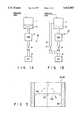
- FIG. 1Ais a schematic view showing a conventional ECR plasma CVD apparatus 10.
- reference numeral 11denotes a plasma processing chamber constituted by an airtight vessel.
- a turbo molecular pump 13is connected to this plasma processing chamber 11 via a gate valve 12.
- a dry pump 15is connected to this turbo molecular pump 13 via a valve 14.
- a molecular drag pumpmay be used instead of the turbo molecular pump 13.
- the film deposition process according to the ECR plasma CVD methodis performed as follows. First, the gate valve 12 are opened. In this condition, the turbo molecular pump 13 and the dry pump 15 are driven to keep the interior of the plasma processing chamber 11 in a high vacuum condition.
- the high vacuum conditionis, for example, pressure of several mTorr.
- a target objectis placed, and a process gas is introduced to perform a film deposition process.
- reaction productsare deposited not only on the target object but also on any surface of the inside of the plasma processing chamber 11.
- in situ cleaningis regularly performed inside the plasma processing chamber 11.
- a plasma for cleaningis generated in the plasma processing chamber 11 to remove reaction products deposited inside the plasma processing chamber 11 by etching.
- Such a cleaning processis normally performed in an atmosphere of a higher pressure than the pressure of a normal film deposition process.
- the pressure for the cleaning processis, for example, several Torr.
- the pressure for the cleaning processis higher than an maximum pressure 0.5 m Torr in which the turbo molecular pump 13 can operate. Therefore, the turbo molecular pump 13 must be temporarily stopped in the above in situ cleaning. However, if the turbo molecular pump 13 is stopped every cleaning process, the production efficiency is greatly decreased because the start and stop of the normal turbo molecular pump 13 require 15 minutes and 10 minutes, respectively.
- a bypass exhaust pipe 16is connected to between a plasma processing chamber 11 to a pipe which couples a valve 14 to a dry pump 15, as shown in FIG. 1B.
- a valve 17is provided on the bypass exhaust pipe 16.
- an ECR plasma CVD apparatus 10' having such a bypassin a cleaning process, the gate valve 12 is closed, and the valve 17 is opened to perform an exhaust operation by the bypass exhaust pipe 16 and the dry pump 15 while a turbo molecular pump 13 is activated. With this operation, the internal pressure of the turbo molecular pump 13 is kept at a high vacuum degree, so that the normal operation of the turbo molecular pump is ensured. Accordingly, the cleaning process can be executed without stopping the turbo molecular pump 13.
- bypass exhaust pipe 16 and the valve 17(to be referred to as a bypass line hereinafter) are provided like in the above ECR plasma CVD apparatus 10', however, generation source, and a target object is more likely the apparatus is bulky and complicated due to the bypass line.
- the turbo molecular pump 13To set the interior of the plasma processing chamber 11 to the high vacuum condition, it is preferable to arrange the turbo molecular pump 13 near the plasma processing chamber 11 as close as possible. Therefore, the gate valve 12 is arranged very near the plasma processing chamber 11. Owing to this arrangement, reaction products tend to attach to the inside of the gate valve 12 to cause generation of particles, resulting in a decrease in yield. Moreover, since the gate valve 12 is near the plasma processing chamber 11, an O-ring, a bearing, and the like of the gate valve 12 may be damaged by a plasma generated in the plasma processing chamber 11 in film deposition, decreasing the reliability and the production efficiency.
- the present inventionprovides a semiconductor processing apparatus for ECR plasma CVD, comprising:
- a plasma generation chamberto which a microwave and a plasma source gas are introduced
- an excitation solenoidsurrounding the plasma generation chamber, for forming an electron cyclotron resonance magnetic field with the microwave in the plasma generation chamber;
- a plasma reaction chamberwhich is provided in communication with the plasma generation chamber and to which a reactive gas is introduced;
- a leakage-type valvewhich is provided in communication with the plasma reaction chamber and whose opening degree can be freely controlled;
- a high-vacuum pumpcoupled to an outlet of the leakage-type valve
- cleaning gas supply meansfor supplying a cleaning gas into the plasma reaction chamber
- a sub-pumpcoupled to an outlet of the high-vacuum pump.
- the present inventionprovides a method of cleaning a semiconductor processing apparatus for ECR plasma CVD which comprises: a plasma generation chamber to which a microwave and a plasma source gas are introduced; an excitation solenoid, surrounding the plasma generation chamber, for forming an electron cyclotron resonance magnetic field with the microwave in the plasma generation chamber; a plasma reaction chamber which is provided in communication with the plasma generation chamber and to which a reactive gas is introduced; holding means, set in the plasma reaction chamber, for holding a target object; a leakage-type valve which is provided in communication with the plasma reaction chamber and whose opening degree can be freely controlled; a high-vacuum pump coupled to an outlet of the leakage-type valve; and a sub-pump coupled to an outlet of the high-vacuum pump, comprising the steps of:
- FIGS. 1A and 1Bare schematic views showing conventional ECR plasma CVD apparatuses, respectively;
- FIG. 2is a schematic view showing an example of an ECR plasma CVD apparatus according to the present invention.
- FIG. 3is a sectional view showing a butterfly valve of the ECR plasma CVD apparatus shown in FIG. 2.
- FIG. 2shows an example of an ECR plasma CVD apparatus according to the present invention.
- a waveguide 21is connected to a microwave power supply 19.
- the waveguide 21is connected to a plasma generation chamber 23.
- a waveguide window 22is set between the waveguide 21 and the plasma generation chamber 23.
- An excitation solenoid 24is set around the plasma generation chamber 23.
- a first gas feed system 25 for introducing a gas into the plasma generation chamber 23is connected to the plasma generation chamber 23.
- the first gas feed system 25is connected to a cleaning gas supply source 18, a nitrogen gas supply source 44, F doping gas supply source 46, and, an oxygen gas supply source 47.
- a plasma reaction chamber 26is continuously arranged under the plasma generation chamber 23.
- a plasma extraction window 27is set between the plasma generation chamber 23 and the plasma reaction chamber 26.
- a plasma flowis extracted to the plasma reaction chamber 26 via the plasma extraction window 27.
- a second gas feed system 28 and a third gas feed system 45are connected to the plasma reaction chamber 26.
- a substrate holder 29is set in the plasma reaction chamber 26 at a downstream position from the inlet port of the second gas feed system 28.
- the second gas feed system 28is connected to a silane gas supply source 43 while the third gas feed system 45 is connected to a F doping gas supply source 46.
- a sub-solenoid 30is arranged on the lower surface side of the substrate holder 29 so as to be coaxial with the excitation solenoid 24.
- the sub-solenoid 30generates a magnetic field having a reverse direction to that of the excitation solenoid 24, thereby forming a mirror or cusped magnetic field around a substrate W.
- An RF power supply 31is connected to the substrate holder 29.
- Two exhaust ports 32 and 33are formed in the side wall surface of the plasma reaction chamber 26 at positions symmetrical about the center of the plasma reaction chamber 26.
- Leakage-type butterfly valves 34 and 35are provided at the lower portions of the exhaust ports 32 and 33, respectively.
- turbo molecular pumps 36 and 37are connected on the downstream sides of the butterfly valves 34 and 35, respectively. These turbo molecular pumps 36 and 37 are used for setting the interior of the plasma reaction chamber 26 to a high vacuum atmosphere.
- a high vacuummeans a pressure of, e.g., several mTorr, and more particularly, a pressure within the range from 0.5 to 5 mTorr. Formation of such a high vacuum atmosphere needs a pump having a large discharge amount and an ability of accomplishing the high vacuum.
- a pumpis required for a discharge amount of 1000 to 3000 l/sec and a pressure which the pump can generate (to be referred to as generatable-pressure hereinafter), of 10 -6 to 10 -8 mTorr.
- the pump to be used in this apparatusis not limited to the turbo molecular pumps 36 and 37, and any pump can be used, provided that it has the equal discharge amount and generatable-pressure to those of the turbo molecular pumps 36 and 37. Note that such a pump is called a high-vacuum pump.
- Exhaust pipes 38 and 39are connected to the turbo molecular pumps 36 and 37, respectively.
- the exhaust pipes 38 and 39are coupled together to one pipe, which is connected to a dry pump 41 via a control valve 40.
- This dry pump 41is used to reduce the pressure in the plasma reaction chamber 26 to a pressure at which the turbo molecular pumps 36 and 37 can be driven before driving the turbo molecular pumps 36 and 37.
- a pump(to be referred to as a sub-pump hereinafter) used for this preliminary pressure reduction need not have a large discharge amount and a high generatable-pressure, unlike the turbo molecular pumps 36 and 37.
- Any sub-pumpcan be used, provided that it has a discharge amount of, for example, 20 to 80 l/sec and a generatable-pressure of, for example, 1 to 5 mTorr.
- FIG. 3shows an example of the butterfly valve 34, 35.
- the butterfly valve 34, 35is constituted by a rotary shaft 50, a flapper 51 constituted to be rotatable about the rotary shaft 50, a driving mechanism (not shown in the figure), and an inner pipe wall 52.
- the angle of the flapper 51is changed by rotating the rotary shaft 50 by the driving mechanism to adjust the opening degree of a gap between the flapper 51 and the inner pipe wall 52.
- the size of the flapper 51is designed to have a slight gap (e.g., a gap of about 0.1 mm) between the flapper 51 and the inner pipe wall 52 in a condition wherein the flapper 51 is completely closed, i.e., in a condition wherein the flapper 51 is substantially horizontal (to be referred to as a full closed condition hereinafter), as represented by a solid line in FIG. 3.
- a slight gape.g., a gap of about 0.1 mm
- the present inventioncan use the valve which allows a slight air flow to generate even in the complete closed condition.
- a valveis called a leakage-type valve.
- the silicon wafer Wis placed on the substrate holder 29.
- the butterfly valves 34 and 35are set in a full open condition, and at the same time the control valve 40 is also in a full open condition.
- the dry pump 41is activated to reduce the pressure in the plasma reaction chamber 26 to the range of 0.1 to 1 Torr.
- the two turbo molecular pumps 36 and 37are operated to decrease the pressure in the plasma reaction chamber 26 to a predetermined high vacuum of, e.g., several mTorr, and more particularly, to the range of 0.5 to 5 mTorr. This internal condition is kept.
- a microwave generated by the microwave power supply 19is introduced into the plasma generation chamber 23 via the waveguide 21 and the waveguide window 22.
- the oxygen gas as a plasma source gasis introduced from the first gas feed system 25 to the plasma generation chamber 23 to generate a plasma.
- the generated plasmais extracted to the plasma reaction chamber 26 due to an electron cyclotron resonance magnetic field formed by the excitation solenoid 24.
- the silane gas as reactive gasesare introduced into the plasma reaction chamber 26 via the second gas feed system 28.
- the introduced silane gasis decomposed by the energy of the plasma.
- the decomposition products of the silane gasare deposited on the surface of the wafer W placed on the substrate holder 29 due to a mirror magnetic field area formed around the substrate holder 29 by the excitation solenoid 24 and the sub-solenoid 30, thereby forming a silicon oxide film.
- the following cleaning processis performed to remove the silicon oxide film attached to the inner wall surface of the plasma reaction chamber 26 and the two surfaces 51a and 51b of the flappers 51 of the butterfly valves 34 and 35.
- the two butterfly valves 34 and 35are set in the full closed condition with the two turbo molecular pumps 36 and 37 and the dry pump 41 being kept operating. Simultaneously, the control valve 40 can be closed to a certain degree to limit evacuation. With this operation, the pressure in the plasma reaction chamber 26 is set to a low vacuum atmosphere in which the turbo molecular pumps 36 and 37 can be driven, e.g., to several Torr, and more particularly, within the range of 0.1 to 2 Torr. Note that another means for increasing the pressure in the plasma reaction chamber 26 is to decrease the rotational speeds of the turbo molecular pumps 36 and 37.
- a cleaning gas(e.g., NF 3 ) is supplied via the first gas feed system 25 to the plasma reaction chamber 26 in such a low vacuum atmosphere.
- a plasmais generated. This removes the silicon oxide films deposited in the plasma generation chamber 23, the plasma reaction chamber 26 and on the exhaust ports 32 and 33 and the surfaces of the butterfly valves 34 and 35.
- the butterfly valves 34 and 35are in the full closed condition, one surface of each of the flappers 51 of the butterfly valves 34 and 35 faces upward, i.e., to the direction of the plasma reaction chamber 26. With this arrangement, the plasma generated in the plasma reaction chamber 26 cleans one surface of each flapper 51.
- each flapper 51In the film deposition process, however, the flappers 51 are in the substantially vertical condition, so that the silicon oxide film is deposited on two surfaces 51a and 51b of each flapper 51. Accordingly, it is preferable that the flappers 51 of the butterfly valves 34 and 35 used in the present invention be rotatable substantially through 180° on the basis of the horizontal direction. In this case, each flapper 51 can rotate from a full closed condition wherein one surface 51a faces upward to a full closed condition wherein the other surface 51b faces upward, as indicated by arrows A in FIG. 3. With this arrangement, the two surfaces 51a and 51b of the flapper 51 can be faced upward, i.e., to the direction of the plasma reaction chamber 26.
- the plasma generated in the plasma reaction chamber 26can clean the two surfaces 51a and 51b of the flapper 51.
- the silicon oxide film deposited on one surface 51a of the flapper 51is removed.
- the silicon oxide film on the other surface 51b of the flapper 51is removed. As a result, it can be avoided that any one surface of the flapper 51 is not cleaned, and that the silicon oxide film is left uncleaned on the surface.
- the butterfly valves 34 and 35are of the leakage type. Therefore, a slight gas flow is formed even in the full closed condition. For this reason, the present invention has an advantage the cleaning process can be performed while the turbo molecular pumps 36 and 37 drive.
- the butterfly valves 34 and 35do not use an O-ring having a large bore diameter and the like, unlike a gate valve. Accordingly, for example, the butterfly valves 34 and 35 are free from degradation caused by the influence of a cleaning plasma to avoid a decrease in service life. Further, maintenance need not be frequently performed.
- the turbo molecular pumps 36 and 37need not be stopped every cleaning process. For this reason, the stop and start operations of the turbo molecular pumps 36 and 37 can be omitted to shorten a time required for a cleaning process.
- the ECR plasma CVD apparatus 20 of this embodimentdoes not require a bypass line, unlike in FIG. 1B. For this reason, a smaller and simpler apparatus can be realized. Also, maintenance of a bypass line is not required.
- an air flow from the plasma reaction chamber 26 to the turbo molecular pumps 36 and 37depends on a viscous flow when a pressure in the plasma reaction chamber 26 becomes a low vacuum.
- the turbo molecular pumps 36 and 37are preferably attached to positions symmetrical about the center of the plasma reaction chamber 26, as described above.
- the turbo molecular pumps 36 and 37are preferably attached to positions near the plasma reaction chamber 26 as close as possible.
Landscapes
- Chemical & Material Sciences (AREA)
- Engineering & Computer Science (AREA)
- Physics & Mathematics (AREA)
- Plasma & Fusion (AREA)
- Metallurgy (AREA)
- Mechanical Engineering (AREA)
- Organic Chemistry (AREA)
- Materials Engineering (AREA)
- Chemical Kinetics & Catalysis (AREA)
- General Chemical & Material Sciences (AREA)
- Analytical Chemistry (AREA)
- General Physics & Mathematics (AREA)
- Manufacturing & Machinery (AREA)
- Power Engineering (AREA)
- Computer Hardware Design (AREA)
- Condensed Matter Physics & Semiconductors (AREA)
- Microelectronics & Electronic Packaging (AREA)
- Chemical Vapour Deposition (AREA)
- Drying Of Semiconductors (AREA)
- Cleaning Or Drying Semiconductors (AREA)
Abstract
Description
Claims (9)
Applications Claiming Priority (2)
| Application Number | Priority Date | Filing Date | Title |
|---|---|---|---|
| JP06196535AJP3107275B2 (en) | 1994-08-22 | 1994-08-22 | Semiconductor manufacturing apparatus and semiconductor manufacturing apparatus cleaning method |
| JP6-196535 | 1994-08-22 |
Publications (1)
| Publication Number | Publication Date |
|---|---|
| US5611863Atrue US5611863A (en) | 1997-03-18 |
Family
ID=16359362
Family Applications (1)
| Application Number | Title | Priority Date | Filing Date |
|---|---|---|---|
| US08/517,286Expired - Fee RelatedUS5611863A (en) | 1994-08-22 | 1995-08-21 | Semiconductor processing apparatus and cleaning method thereof |
Country Status (4)
| Country | Link |
|---|---|
| US (1) | US5611863A (en) |
| JP (1) | JP3107275B2 (en) |
| KR (1) | KR100316300B1 (en) |
| TW (1) | TW353763B (en) |
Cited By (27)
| Publication number | Priority date | Publication date | Assignee | Title |
|---|---|---|---|---|
| US6125859A (en)* | 1997-03-05 | 2000-10-03 | Applied Materials, Inc. | Method for improved cleaning of substrate processing systems |
| EP0794267A3 (en)* | 1996-03-08 | 2000-10-04 | Applied Materials, Inc. | A restrictor shield for a wafer processing apparatus |
| US6248206B1 (en)* | 1996-10-01 | 2001-06-19 | Applied Materials Inc. | Apparatus for sidewall profile control during an etch process |
| US6274058B1 (en) | 1997-07-11 | 2001-08-14 | Applied Materials, Inc. | Remote plasma cleaning method for processing chambers |
| SG87109A1 (en)* | 1999-05-10 | 2002-03-19 | Eaton Corp | System and method for cleaning silicon-coated surfaces in an ion implanter |
| US6410408B1 (en)* | 2000-08-31 | 2002-06-25 | Matsushita Electric Industrial Co., Ltd. | CVD film formation method |
| US20030170403A1 (en)* | 2002-03-11 | 2003-09-11 | Doan Trung Tri | Atomic layer deposition apparatus and method |
| US6641698B2 (en)* | 2000-12-22 | 2003-11-04 | Lsi Logic Corporation | Integrated circuit fabrication dual plasma process with separate introduction of different gases into gas flow |
| WO2004001230A1 (en)* | 2002-06-20 | 2003-12-31 | The Boc Group Plc | Apparatus for controlling the pressure in a process chamber and method of operating same |
| EP1150332A3 (en)* | 2000-04-28 | 2005-03-23 | Applied Materials, Inc. | Integration of remote plasma generator with semiconductor processing chamber |
| US20050120955A1 (en)* | 2002-07-10 | 2005-06-09 | Tokyo Electron Limited | Film forming apparatus |
| WO2005071268A1 (en)* | 2004-01-23 | 2005-08-04 | The Boc Group Plc | Screw vacuum pump |
| SG116411A1 (en)* | 2000-01-28 | 2005-11-28 | Applied Materials Inc | Method and apparatus for cleaning a semiconductor wafer processing system. |
| US20060162656A1 (en)* | 2002-07-31 | 2006-07-27 | Tokyo Electron Limited | Reduced volume, high conductance process chamber |
| SG156522A1 (en)* | 2002-12-18 | 2009-11-26 | Taiwan Semiconductor Mfg | Multi-phase pressure control valve for process chamber |
| US8075789B1 (en) | 1997-07-11 | 2011-12-13 | Applied Materials, Inc. | Remote plasma cleaning source having reduced reactivity with a substrate processing chamber |
| FR2965888A1 (en)* | 2010-10-08 | 2012-04-13 | Alcatel Lucent | GAS DRAIN PIPING AND ASSOCIATED DRAINAGE METHOD |
| US20120111427A1 (en)* | 2008-08-28 | 2012-05-10 | Tokyo Electron Limited | Plasma processing apparatus, plasma processing method, method for cleaning plasma processing apparatus and pressure control valve for plasma processing apparatus |
| US20130001194A1 (en)* | 2011-06-30 | 2013-01-03 | Jaemin Roh | Apparatuses and methods for treating substrate |
| US20130239663A1 (en)* | 2006-12-27 | 2013-09-19 | Hitachi High-Technologies Corporation | Apparatus for evaluating lubrican |
| US20130239889A1 (en)* | 2012-03-14 | 2013-09-19 | Taiwan Semiconductor Manufacturing Co., Ltd. | Valve purge assembly for semiconductor manufacturing tools |
| US20150211114A1 (en)* | 2014-01-30 | 2015-07-30 | Applied Materials, Inc. | Bottom pump and purge and bottom ozone clean hardware to reduce fall-on particle defects |
| CN104701121B (en)* | 2013-12-04 | 2017-01-04 | 中微半导体设备(上海)有限公司 | It is provided with pump and the plasma treatment appts that can improve symmetric gas operated device |
| EP3066369A4 (en)* | 2013-11-08 | 2017-05-17 | MKS Instruments, Inc. | Powder and deposition control in throttle valve |
| US20180111171A1 (en)* | 2016-10-26 | 2018-04-26 | Varian Semiconductor Equipment Associates, Inc. | Apparatus And Method For Differential In Situ Cleaning |
| US10287707B2 (en) | 2016-09-26 | 2019-05-14 | Nuflare Technology, Inc. | Film growth apparatus, film growth method and maintenance method of film growth apparatus |
| US11306824B2 (en)* | 2017-09-29 | 2022-04-19 | Applied Materials, Inc. | Dual port remote plasma clean isolation valve |
Families Citing this family (7)
| Publication number | Priority date | Publication date | Assignee | Title |
|---|---|---|---|---|
| US6357385B1 (en)* | 1997-01-29 | 2002-03-19 | Tadahiro Ohmi | Plasma device |
| JP3563565B2 (en)* | 1997-06-09 | 2004-09-08 | 東京エレクトロン株式会社 | Exhaust device and exhaust method |
| US7428915B2 (en)* | 2005-04-26 | 2008-09-30 | Applied Materials, Inc. | O-ringless tandem throttle valve for a plasma reactor chamber |
| JP4870536B2 (en)* | 2006-12-06 | 2012-02-08 | 株式会社ニューフレアテクノロジー | Vapor growth method |
| KR101586237B1 (en)* | 2015-07-24 | 2016-01-19 | 주식회사 애니테이프 | Lubricants removal apparatus using atomospheric plasma |
| JP7684219B2 (en)* | 2019-09-25 | 2025-05-27 | 芝浦機械株式会社 | Flow control valve, pump unit and surface treatment device |
| JPWO2024057588A1 (en)* | 2022-09-14 | 2024-03-21 |
Citations (9)
| Publication number | Priority date | Publication date | Assignee | Title |
|---|---|---|---|---|
| JPS6179747A (en)* | 1984-09-28 | 1986-04-23 | Santoku Kinzoku Kogyo Kk | Permanent magnet alloy |
| JPS61101029A (en)* | 1984-10-24 | 1986-05-19 | Hitachi Ltd | Coating device |
| JPS61174623A (en)* | 1985-01-29 | 1986-08-06 | Toshiba Corp | Sample processing equipment |
| US4816113A (en)* | 1987-02-24 | 1989-03-28 | Semiconductor Energy Laboratory Co., Ltd. | Method of eliminating undesirable carbon product deposited on the inside of a reaction chamber |
| US4971667A (en)* | 1988-02-05 | 1990-11-20 | Semiconductor Energy Laboratory Co., Ltd. | Plasma processing method and apparatus |
| JPH0533138A (en)* | 1991-07-30 | 1993-02-09 | Fuji Electric Co Ltd | Method of manufacturing oxide film |
| JPH05117867A (en)* | 1991-09-02 | 1993-05-14 | Fuji Electric Co Ltd | Method and apparatus for producing silicon oxide film |
| US5368685A (en)* | 1992-03-24 | 1994-11-29 | Hitachi, Ltd. | Dry etching apparatus and method |
| US5512102A (en)* | 1985-10-14 | 1996-04-30 | Semiconductor Energy Laboratory Co., Ltd. | Microwave enhanced CVD system under magnetic field |
Family Cites Families (7)
| Publication number | Priority date | Publication date | Assignee | Title |
|---|---|---|---|---|
| JPS5987134U (en)* | 1982-12-03 | 1984-06-13 | 株式会社日立製作所 | semiconductor manufacturing equipment |
| JPS60176544U (en)* | 1984-04-28 | 1985-11-22 | 沖電気工業株式会社 | Thin film forming equipment |
| JPS63205914A (en)* | 1987-02-23 | 1988-08-25 | Hitachi Ltd | semiconductor manufacturing equipment |
| JPH01161836A (en)* | 1987-12-18 | 1989-06-26 | Nec Corp | Vacuum treatment device |
| JPH0252428A (en)* | 1988-08-16 | 1990-02-22 | Tokyo Electron Ltd | Treatment apparatus |
| JPH0294522A (en)* | 1988-09-30 | 1990-04-05 | Toshiba Corp | Dry etching method |
| JPH03245526A (en)* | 1990-02-22 | 1991-11-01 | Mitsubishi Electric Corp | plasma processing equipment |
- 1994
- 1994-08-22JPJP06196535Apatent/JP3107275B2/ennot_activeExpired - Fee Related
- 1995
- 1995-08-21USUS08/517,286patent/US5611863A/ennot_activeExpired - Fee Related
- 1995-08-22KRKR1019950025954Apatent/KR100316300B1/ennot_activeExpired - Fee Related
- 1995-08-22TWTW084108765Apatent/TW353763B/enactive
Patent Citations (9)
| Publication number | Priority date | Publication date | Assignee | Title |
|---|---|---|---|---|
| JPS6179747A (en)* | 1984-09-28 | 1986-04-23 | Santoku Kinzoku Kogyo Kk | Permanent magnet alloy |
| JPS61101029A (en)* | 1984-10-24 | 1986-05-19 | Hitachi Ltd | Coating device |
| JPS61174623A (en)* | 1985-01-29 | 1986-08-06 | Toshiba Corp | Sample processing equipment |
| US5512102A (en)* | 1985-10-14 | 1996-04-30 | Semiconductor Energy Laboratory Co., Ltd. | Microwave enhanced CVD system under magnetic field |
| US4816113A (en)* | 1987-02-24 | 1989-03-28 | Semiconductor Energy Laboratory Co., Ltd. | Method of eliminating undesirable carbon product deposited on the inside of a reaction chamber |
| US4971667A (en)* | 1988-02-05 | 1990-11-20 | Semiconductor Energy Laboratory Co., Ltd. | Plasma processing method and apparatus |
| JPH0533138A (en)* | 1991-07-30 | 1993-02-09 | Fuji Electric Co Ltd | Method of manufacturing oxide film |
| JPH05117867A (en)* | 1991-09-02 | 1993-05-14 | Fuji Electric Co Ltd | Method and apparatus for producing silicon oxide film |
| US5368685A (en)* | 1992-03-24 | 1994-11-29 | Hitachi, Ltd. | Dry etching apparatus and method |
Cited By (44)
| Publication number | Priority date | Publication date | Assignee | Title |
|---|---|---|---|---|
| EP0794267A3 (en)* | 1996-03-08 | 2000-10-04 | Applied Materials, Inc. | A restrictor shield for a wafer processing apparatus |
| US6248206B1 (en)* | 1996-10-01 | 2001-06-19 | Applied Materials Inc. | Apparatus for sidewall profile control during an etch process |
| US6125859A (en)* | 1997-03-05 | 2000-10-03 | Applied Materials, Inc. | Method for improved cleaning of substrate processing systems |
| US6274058B1 (en) | 1997-07-11 | 2001-08-14 | Applied Materials, Inc. | Remote plasma cleaning method for processing chambers |
| US8075789B1 (en) | 1997-07-11 | 2011-12-13 | Applied Materials, Inc. | Remote plasma cleaning source having reduced reactivity with a substrate processing chamber |
| SG87109A1 (en)* | 1999-05-10 | 2002-03-19 | Eaton Corp | System and method for cleaning silicon-coated surfaces in an ion implanter |
| EP1120814A3 (en)* | 2000-01-28 | 2008-07-30 | Applied Materials, Inc. | Method and apparatus for cleaning a semiconductor wafer processing system |
| SG116411A1 (en)* | 2000-01-28 | 2005-11-28 | Applied Materials Inc | Method and apparatus for cleaning a semiconductor wafer processing system. |
| EP1150332A3 (en)* | 2000-04-28 | 2005-03-23 | Applied Materials, Inc. | Integration of remote plasma generator with semiconductor processing chamber |
| US6410408B1 (en)* | 2000-08-31 | 2002-06-25 | Matsushita Electric Industrial Co., Ltd. | CVD film formation method |
| US6641698B2 (en)* | 2000-12-22 | 2003-11-04 | Lsi Logic Corporation | Integrated circuit fabrication dual plasma process with separate introduction of different gases into gas flow |
| US6893506B2 (en)* | 2002-03-11 | 2005-05-17 | Micron Technology, Inc. | Atomic layer deposition apparatus and method |
| US20050142890A1 (en)* | 2002-03-11 | 2005-06-30 | Doan Trung T. | Atomic layer deposition apparatus and method |
| US20030170403A1 (en)* | 2002-03-11 | 2003-09-11 | Doan Trung Tri | Atomic layer deposition apparatus and method |
| US7030037B2 (en) | 2002-03-11 | 2006-04-18 | Micron Technology, Inc. | Atomic layer deposition apparatus and method |
| US20060144333A1 (en)* | 2002-03-11 | 2006-07-06 | Doan Trung T | Atomic layer deposition apparatus and method |
| US7431773B2 (en) | 2002-03-11 | 2008-10-07 | Micron Technology, Inc. | Atomic layer deposition apparatus and method |
| WO2004001230A1 (en)* | 2002-06-20 | 2003-12-31 | The Boc Group Plc | Apparatus for controlling the pressure in a process chamber and method of operating same |
| US20050217732A1 (en)* | 2002-06-20 | 2005-10-06 | Tollner Martin E | Apparatus for controlling the pressure in a process chamber and method of operating same |
| US7814922B2 (en) | 2002-06-20 | 2010-10-19 | Edwards Limited | Apparatus for controlling the pressure in a process chamber and method of operating same |
| CN100385123C (en)* | 2002-06-20 | 2008-04-30 | 爱德华兹有限公司 | Apparatus for controlling pressure in a processing chamber and method of operation thereof |
| US20050120955A1 (en)* | 2002-07-10 | 2005-06-09 | Tokyo Electron Limited | Film forming apparatus |
| US20060162656A1 (en)* | 2002-07-31 | 2006-07-27 | Tokyo Electron Limited | Reduced volume, high conductance process chamber |
| SG156522A1 (en)* | 2002-12-18 | 2009-11-26 | Taiwan Semiconductor Mfg | Multi-phase pressure control valve for process chamber |
| US8075288B2 (en) | 2004-01-23 | 2011-12-13 | Edwards Limited | Screw pump and pumping arrangement |
| WO2005071268A1 (en)* | 2004-01-23 | 2005-08-04 | The Boc Group Plc | Screw vacuum pump |
| US20080226481A1 (en)* | 2004-01-23 | 2008-09-18 | Nigel Paul Schofield | Screw Vacuum Pump |
| US20130239663A1 (en)* | 2006-12-27 | 2013-09-19 | Hitachi High-Technologies Corporation | Apparatus for evaluating lubrican |
| US9574267B2 (en)* | 2008-08-28 | 2017-02-21 | Tokyo Electron Limited | Plasma processing apparatus |
| US9631274B2 (en)* | 2008-08-28 | 2017-04-25 | Tokyo Electron Limited | Plasma processing apparatus |
| US20120111427A1 (en)* | 2008-08-28 | 2012-05-10 | Tokyo Electron Limited | Plasma processing apparatus, plasma processing method, method for cleaning plasma processing apparatus and pressure control valve for plasma processing apparatus |
| US20150159269A1 (en)* | 2008-08-28 | 2015-06-11 | Tokyo Electron Limited | Plasma processing apparatus |
| US8973527B2 (en)* | 2008-08-28 | 2015-03-10 | Tokyo Electron Limited | Plasma processing apparatus, plasma processing method, method for cleaning plasma processing apparatus and pressure control valve for plasma processing apparatus |
| FR2965888A1 (en)* | 2010-10-08 | 2012-04-13 | Alcatel Lucent | GAS DRAIN PIPING AND ASSOCIATED DRAINAGE METHOD |
| US9418880B2 (en)* | 2011-06-30 | 2016-08-16 | Semes Co., Ltd. | Apparatuses and methods for treating substrate |
| US20130001194A1 (en)* | 2011-06-30 | 2013-01-03 | Jaemin Roh | Apparatuses and methods for treating substrate |
| US20130239889A1 (en)* | 2012-03-14 | 2013-09-19 | Taiwan Semiconductor Manufacturing Co., Ltd. | Valve purge assembly for semiconductor manufacturing tools |
| EP3066369A4 (en)* | 2013-11-08 | 2017-05-17 | MKS Instruments, Inc. | Powder and deposition control in throttle valve |
| CN104701121B (en)* | 2013-12-04 | 2017-01-04 | 中微半导体设备(上海)有限公司 | It is provided with pump and the plasma treatment appts that can improve symmetric gas operated device |
| US20150211114A1 (en)* | 2014-01-30 | 2015-07-30 | Applied Materials, Inc. | Bottom pump and purge and bottom ozone clean hardware to reduce fall-on particle defects |
| US10287707B2 (en) | 2016-09-26 | 2019-05-14 | Nuflare Technology, Inc. | Film growth apparatus, film growth method and maintenance method of film growth apparatus |
| US20180111171A1 (en)* | 2016-10-26 | 2018-04-26 | Varian Semiconductor Equipment Associates, Inc. | Apparatus And Method For Differential In Situ Cleaning |
| US10730082B2 (en)* | 2016-10-26 | 2020-08-04 | Varian Semiconductor Equipment Associates, Inc. | Apparatus and method for differential in situ cleaning |
| US11306824B2 (en)* | 2017-09-29 | 2022-04-19 | Applied Materials, Inc. | Dual port remote plasma clean isolation valve |
Also Published As
| Publication number | Publication date |
|---|---|
| TW353763B (en) | 1999-03-01 |
| KR960008971A (en) | 1996-03-22 |
| JPH0864578A (en) | 1996-03-08 |
| KR100316300B1 (en) | 2002-04-24 |
| JP3107275B2 (en) | 2000-11-06 |
Similar Documents
| Publication | Publication Date | Title |
|---|---|---|
| US5611863A (en) | Semiconductor processing apparatus and cleaning method thereof | |
| US11986868B2 (en) | System dedicated for parts cleaning | |
| JP3501524B2 (en) | Vacuum exhaust system for processing equipment | |
| US7964040B2 (en) | Multi-port pumping system for substrate processing chambers | |
| US7077159B1 (en) | Processing apparatus having integrated pumping system | |
| JP3667202B2 (en) | Substrate processing equipment | |
| US20030119328A1 (en) | Plasma processing apparatus, and cleaning method therefor | |
| CN100539029C (en) | Plasma doping method and plasma processing apparatus | |
| US20250197993A1 (en) | Vacuuming ststem, semiconductor process device and vacuuming method thereof | |
| US20130239889A1 (en) | Valve purge assembly for semiconductor manufacturing tools | |
| JP4244674B2 (en) | Processing apparatus and processing method | |
| US20060065194A1 (en) | Diffuser and semiconductor device manufacturing equipment having the same | |
| WO2022086788A1 (en) | Methods of seasoning process chambers | |
| JP3595508B2 (en) | Semiconductor manufacturing equipment | |
| JP3173681B2 (en) | Evacuation apparatus and method | |
| JPH0982594A (en) | Indoor decompression method for semiconductor manufacturing equipment | |
| KR102612086B1 (en) | Particle free remote plasma source isolation valve | |
| JP2003229417A (en) | Vacuum processing apparatus and method of controlling the same | |
| KR20250096354A (en) | Semiconductor manufacturing equipment | |
| JP2001338891A (en) | Apparatus for manufacturing semiconductor device | |
| JPH0310072A (en) | Magnetron sputtering equipment | |
| KR100222960B1 (en) | Pumping Line for Low Pressure Process | |
| KR20210052849A (en) | Gas valve assembly and substrate processing apparatus having the same | |
| JPH11222678A (en) | Film forming device | |
| KR19990074646A (en) | Dry etching equipment of semiconductor device manufacturing equipment |
Legal Events
| Date | Code | Title | Description |
|---|---|---|---|
| AS | Assignment | Owner name:TOKYO ELECTRON TOHOKU LIMITED, JAPAN Free format text:ASSIGNMENT OF ASSIGNORS INTEREST;ASSIGNOR:MIYAGI, KATSUSHIN;REEL/FRAME:007623/0562 Effective date:19950804 Owner name:TOKYO ELECTRON LIMITED, JAPAN Free format text:ASSIGNMENT OF ASSIGNORS INTEREST;ASSIGNOR:MIYAGI, KATSUSHIN;REEL/FRAME:007623/0562 Effective date:19950804 | |
| AS | Assignment | Owner name:TOKYO ELECTRON LIMITED, JAPAN Free format text:ASSIGNMENT OF ASSIGNORS INTEREST;ASSIGNOR:TOKYO ELECTRON TOHOKU LIMITED;REEL/FRAME:008595/0021 Effective date:19961127 | |
| FEPP | Fee payment procedure | Free format text:PAYOR NUMBER ASSIGNED (ORIGINAL EVENT CODE: ASPN); ENTITY STATUS OF PATENT OWNER: LARGE ENTITY | |
| FPAY | Fee payment | Year of fee payment:4 | |
| FEPP | Fee payment procedure | Free format text:PAYER NUMBER DE-ASSIGNED (ORIGINAL EVENT CODE: RMPN); ENTITY STATUS OF PATENT OWNER: LARGE ENTITY Free format text:PAYOR NUMBER ASSIGNED (ORIGINAL EVENT CODE: ASPN); ENTITY STATUS OF PATENT OWNER: LARGE ENTITY | |
| REMI | Maintenance fee reminder mailed | ||
| LAPS | Lapse for failure to pay maintenance fees | ||
| STCH | Information on status: patent discontinuation | Free format text:PATENT EXPIRED DUE TO NONPAYMENT OF MAINTENANCE FEES UNDER 37 CFR 1.362 | |
| FP | Lapsed due to failure to pay maintenance fee | Effective date:20050318 |