US5610442A - Semiconductor device package fabrication method and apparatus - Google Patents
Semiconductor device package fabrication method and apparatusDownload PDFInfo
- Publication number
- US5610442A US5610442AUS08/412,087US41208795AUS5610442AUS 5610442 AUS5610442 AUS 5610442AUS 41208795 AUS41208795 AUS 41208795AUS 5610442 AUS5610442 AUS 5610442A
- Authority
- US
- United States
- Prior art keywords
- package
- planar substrate
- semiconductor device
- wiring board
- printed wiring
- Prior art date
- Legal status (The legal status is an assumption and is not a legal conclusion. Google has not performed a legal analysis and makes no representation as to the accuracy of the status listed.)
- Expired - Lifetime
Links
Images


Classifications
- H—ELECTRICITY
- H01—ELECTRIC ELEMENTS
- H01L—SEMICONDUCTOR DEVICES NOT COVERED BY CLASS H10
- H01L24/00—Arrangements for connecting or disconnecting semiconductor or solid-state bodies; Methods or apparatus related thereto
- H01L24/01—Means for bonding being attached to, or being formed on, the surface to be connected, e.g. chip-to-package, die-attach, "first-level" interconnects; Manufacturing methods related thereto
- H01L24/26—Layer connectors, e.g. plate connectors, solder or adhesive layers; Manufacturing methods related thereto
- H01L24/31—Structure, shape, material or disposition of the layer connectors after the connecting process
- H01L24/32—Structure, shape, material or disposition of the layer connectors after the connecting process of an individual layer connector
- H—ELECTRICITY
- H01—ELECTRIC ELEMENTS
- H01L—SEMICONDUCTOR DEVICES NOT COVERED BY CLASS H10
- H01L23/00—Details of semiconductor or other solid state devices
- H01L23/28—Encapsulations, e.g. encapsulating layers, coatings, e.g. for protection
- H01L23/31—Encapsulations, e.g. encapsulating layers, coatings, e.g. for protection characterised by the arrangement or shape
- H01L23/3107—Encapsulations, e.g. encapsulating layers, coatings, e.g. for protection characterised by the arrangement or shape the device being completely enclosed
- H01L23/3121—Encapsulations, e.g. encapsulating layers, coatings, e.g. for protection characterised by the arrangement or shape the device being completely enclosed a substrate forming part of the encapsulation
- H01L23/3128—Encapsulations, e.g. encapsulating layers, coatings, e.g. for protection characterised by the arrangement or shape the device being completely enclosed a substrate forming part of the encapsulation the substrate having spherical bumps for external connection
- H—ELECTRICITY
- H01—ELECTRIC ELEMENTS
- H01L—SEMICONDUCTOR DEVICES NOT COVERED BY CLASS H10
- H01L23/00—Details of semiconductor or other solid state devices
- H01L23/34—Arrangements for cooling, heating, ventilating or temperature compensation ; Temperature sensing arrangements
- H01L23/42—Fillings or auxiliary members in containers or encapsulations selected or arranged to facilitate heating or cooling
- H01L23/433—Auxiliary members in containers characterised by their shape, e.g. pistons
- H01L23/4334—Auxiliary members in encapsulations
- H—ELECTRICITY
- H01—ELECTRIC ELEMENTS
- H01L—SEMICONDUCTOR DEVICES NOT COVERED BY CLASS H10
- H01L2224/00—Indexing scheme for arrangements for connecting or disconnecting semiconductor or solid-state bodies and methods related thereto as covered by H01L24/00
- H01L2224/01—Means for bonding being attached to, or being formed on, the surface to be connected, e.g. chip-to-package, die-attach, "first-level" interconnects; Manufacturing methods related thereto
- H01L2224/10—Bump connectors; Manufacturing methods related thereto
- H01L2224/15—Structure, shape, material or disposition of the bump connectors after the connecting process
- H01L2224/16—Structure, shape, material or disposition of the bump connectors after the connecting process of an individual bump connector
- H01L2224/161—Disposition
- H01L2224/16151—Disposition the bump connector connecting between a semiconductor or solid-state body and an item not being a semiconductor or solid-state body, e.g. chip-to-substrate, chip-to-passive
- H01L2224/16221—Disposition the bump connector connecting between a semiconductor or solid-state body and an item not being a semiconductor or solid-state body, e.g. chip-to-substrate, chip-to-passive the body and the item being stacked
- H01L2224/16225—Disposition the bump connector connecting between a semiconductor or solid-state body and an item not being a semiconductor or solid-state body, e.g. chip-to-substrate, chip-to-passive the body and the item being stacked the item being non-metallic, e.g. insulating substrate with or without metallisation
- H01L2224/16227—Disposition the bump connector connecting between a semiconductor or solid-state body and an item not being a semiconductor or solid-state body, e.g. chip-to-substrate, chip-to-passive the body and the item being stacked the item being non-metallic, e.g. insulating substrate with or without metallisation the bump connector connecting to a bond pad of the item
- H—ELECTRICITY
- H01—ELECTRIC ELEMENTS
- H01L—SEMICONDUCTOR DEVICES NOT COVERED BY CLASS H10
- H01L2224/00—Indexing scheme for arrangements for connecting or disconnecting semiconductor or solid-state bodies and methods related thereto as covered by H01L24/00
- H01L2224/01—Means for bonding being attached to, or being formed on, the surface to be connected, e.g. chip-to-package, die-attach, "first-level" interconnects; Manufacturing methods related thereto
- H01L2224/26—Layer connectors, e.g. plate connectors, solder or adhesive layers; Manufacturing methods related thereto
- H01L2224/2612—Auxiliary members for layer connectors, e.g. spacers
- H—ELECTRICITY
- H01—ELECTRIC ELEMENTS
- H01L—SEMICONDUCTOR DEVICES NOT COVERED BY CLASS H10
- H01L2224/00—Indexing scheme for arrangements for connecting or disconnecting semiconductor or solid-state bodies and methods related thereto as covered by H01L24/00
- H01L2224/01—Means for bonding being attached to, or being formed on, the surface to be connected, e.g. chip-to-package, die-attach, "first-level" interconnects; Manufacturing methods related thereto
- H01L2224/42—Wire connectors; Manufacturing methods related thereto
- H01L2224/47—Structure, shape, material or disposition of the wire connectors after the connecting process
- H01L2224/48—Structure, shape, material or disposition of the wire connectors after the connecting process of an individual wire connector
- H01L2224/4805—Shape
- H01L2224/4809—Loop shape
- H01L2224/48091—Arched
- H—ELECTRICITY
- H01—ELECTRIC ELEMENTS
- H01L—SEMICONDUCTOR DEVICES NOT COVERED BY CLASS H10
- H01L2224/00—Indexing scheme for arrangements for connecting or disconnecting semiconductor or solid-state bodies and methods related thereto as covered by H01L24/00
- H01L2224/01—Means for bonding being attached to, or being formed on, the surface to be connected, e.g. chip-to-package, die-attach, "first-level" interconnects; Manufacturing methods related thereto
- H01L2224/42—Wire connectors; Manufacturing methods related thereto
- H01L2224/47—Structure, shape, material or disposition of the wire connectors after the connecting process
- H01L2224/48—Structure, shape, material or disposition of the wire connectors after the connecting process of an individual wire connector
- H01L2224/481—Disposition
- H01L2224/48151—Connecting between a semiconductor or solid-state body and an item not being a semiconductor or solid-state body, e.g. chip-to-substrate, chip-to-passive
- H01L2224/48221—Connecting between a semiconductor or solid-state body and an item not being a semiconductor or solid-state body, e.g. chip-to-substrate, chip-to-passive the body and the item being stacked
- H01L2224/48225—Connecting between a semiconductor or solid-state body and an item not being a semiconductor or solid-state body, e.g. chip-to-substrate, chip-to-passive the body and the item being stacked the item being non-metallic, e.g. insulating substrate with or without metallisation
- H01L2224/48227—Connecting between a semiconductor or solid-state body and an item not being a semiconductor or solid-state body, e.g. chip-to-substrate, chip-to-passive the body and the item being stacked the item being non-metallic, e.g. insulating substrate with or without metallisation connecting the wire to a bond pad of the item
- H—ELECTRICITY
- H01—ELECTRIC ELEMENTS
- H01L—SEMICONDUCTOR DEVICES NOT COVERED BY CLASS H10
- H01L24/00—Arrangements for connecting or disconnecting semiconductor or solid-state bodies; Methods or apparatus related thereto
- H01L24/01—Means for bonding being attached to, or being formed on, the surface to be connected, e.g. chip-to-package, die-attach, "first-level" interconnects; Manufacturing methods related thereto
- H01L24/42—Wire connectors; Manufacturing methods related thereto
- H01L24/47—Structure, shape, material or disposition of the wire connectors after the connecting process
- H01L24/48—Structure, shape, material or disposition of the wire connectors after the connecting process of an individual wire connector
- H—ELECTRICITY
- H01—ELECTRIC ELEMENTS
- H01L—SEMICONDUCTOR DEVICES NOT COVERED BY CLASS H10
- H01L2924/00—Indexing scheme for arrangements or methods for connecting or disconnecting semiconductor or solid-state bodies as covered by H01L24/00
- H01L2924/0001—Technical content checked by a classifier
- H01L2924/00014—Technical content checked by a classifier the subject-matter covered by the group, the symbol of which is combined with the symbol of this group, being disclosed without further technical details
- H—ELECTRICITY
- H01—ELECTRIC ELEMENTS
- H01L—SEMICONDUCTOR DEVICES NOT COVERED BY CLASS H10
- H01L2924/00—Indexing scheme for arrangements or methods for connecting or disconnecting semiconductor or solid-state bodies as covered by H01L24/00
- H01L2924/01—Chemical elements
- H01L2924/01005—Boron [B]
- H—ELECTRICITY
- H01—ELECTRIC ELEMENTS
- H01L—SEMICONDUCTOR DEVICES NOT COVERED BY CLASS H10
- H01L2924/00—Indexing scheme for arrangements or methods for connecting or disconnecting semiconductor or solid-state bodies as covered by H01L24/00
- H01L2924/01—Chemical elements
- H01L2924/01013—Aluminum [Al]
- H—ELECTRICITY
- H01—ELECTRIC ELEMENTS
- H01L—SEMICONDUCTOR DEVICES NOT COVERED BY CLASS H10
- H01L2924/00—Indexing scheme for arrangements or methods for connecting or disconnecting semiconductor or solid-state bodies as covered by H01L24/00
- H01L2924/01—Chemical elements
- H01L2924/01029—Copper [Cu]
- H—ELECTRICITY
- H01—ELECTRIC ELEMENTS
- H01L—SEMICONDUCTOR DEVICES NOT COVERED BY CLASS H10
- H01L2924/00—Indexing scheme for arrangements or methods for connecting or disconnecting semiconductor or solid-state bodies as covered by H01L24/00
- H01L2924/06—Polymers
- H01L2924/078—Adhesive characteristics other than chemical
- H01L2924/07802—Adhesive characteristics other than chemical not being an ohmic electrical conductor
- H—ELECTRICITY
- H01—ELECTRIC ELEMENTS
- H01L—SEMICONDUCTOR DEVICES NOT COVERED BY CLASS H10
- H01L2924/00—Indexing scheme for arrangements or methods for connecting or disconnecting semiconductor or solid-state bodies as covered by H01L24/00
- H01L2924/10—Details of semiconductor or other solid state devices to be connected
- H01L2924/102—Material of the semiconductor or solid state bodies
- H01L2924/1025—Semiconducting materials
- H01L2924/10251—Elemental semiconductors, i.e. Group IV
- H01L2924/10253—Silicon [Si]
- H—ELECTRICITY
- H01—ELECTRIC ELEMENTS
- H01L—SEMICONDUCTOR DEVICES NOT COVERED BY CLASS H10
- H01L2924/00—Indexing scheme for arrangements or methods for connecting or disconnecting semiconductor or solid-state bodies as covered by H01L24/00
- H01L2924/10—Details of semiconductor or other solid state devices to be connected
- H01L2924/11—Device type
- H01L2924/14—Integrated circuits
- H—ELECTRICITY
- H01—ELECTRIC ELEMENTS
- H01L—SEMICONDUCTOR DEVICES NOT COVERED BY CLASS H10
- H01L2924/00—Indexing scheme for arrangements or methods for connecting or disconnecting semiconductor or solid-state bodies as covered by H01L24/00
- H01L2924/15—Details of package parts other than the semiconductor or other solid state devices to be connected
- H01L2924/151—Die mounting substrate
- H01L2924/153—Connection portion
- H01L2924/1531—Connection portion the connection portion being formed only on the surface of the substrate opposite to the die mounting surface
- H01L2924/15311—Connection portion the connection portion being formed only on the surface of the substrate opposite to the die mounting surface being a ball array, e.g. BGA
- H—ELECTRICITY
- H01—ELECTRIC ELEMENTS
- H01L—SEMICONDUCTOR DEVICES NOT COVERED BY CLASS H10
- H01L2924/00—Indexing scheme for arrangements or methods for connecting or disconnecting semiconductor or solid-state bodies as covered by H01L24/00
- H01L2924/15—Details of package parts other than the semiconductor or other solid state devices to be connected
- H01L2924/151—Die mounting substrate
- H01L2924/153—Connection portion
- H01L2924/1531—Connection portion the connection portion being formed only on the surface of the substrate opposite to the die mounting surface
- H01L2924/15312—Connection portion the connection portion being formed only on the surface of the substrate opposite to the die mounting surface being a pin array, e.g. PGA
- H—ELECTRICITY
- H01—ELECTRIC ELEMENTS
- H01L—SEMICONDUCTOR DEVICES NOT COVERED BY CLASS H10
- H01L2924/00—Indexing scheme for arrangements or methods for connecting or disconnecting semiconductor or solid-state bodies as covered by H01L24/00
- H01L2924/15—Details of package parts other than the semiconductor or other solid state devices to be connected
- H01L2924/181—Encapsulation
- H01L2924/1815—Shape
- H01L2924/1816—Exposing the passive side of the semiconductor or solid-state body
- H01L2924/18161—Exposing the passive side of the semiconductor or solid-state body of a flip chip
Definitions
- This inventionrelates to a method and apparatus for fabricating semiconductor device packages, more particularly, to attaching a thermally conductive stiffener proximate to a face of the semiconductor device for reducing warpage of the semiconductor package, and for improved thermal transfer of heat from the semiconductor device in the package.
- Packaging techniques for integrated circuitshave been developed in an attempt to satisfy demands for miniaturization in the semiconductor industry. Improved methods for miniaturization of integrated circuits enabling the integration of millions of transistor circuit elements onto a single integrated circuit semiconductor die, have resulted in increased emphasis on methods to package the semiconductor die in a reliable and mass producible package.
- PPGAplastic pin grid array
- PBGAplastic ball grid array
- the PPGA and PBGA packagesare particularly adapted to have a large number of external connections through either metal pins or solder balls, respectively.
- the PPGA and PBGA packagesare fabricated from printed wiring boards ("PWB") that may have one or more layers of conductive traces or leads arranged in patterns that facilitate interconnection of the semiconductor die circuit connection pads to the external connection pins or solder balls.
- PPGA and PBGA packagesare more fully illustrated in commonly owned U.S. Pat. No. 5,357,672, by Newman, issued Oct. 25, 1994; and U.S. patent application Ser. No. 08/142,251, by Barber, filed Oct. 22, 1993, both incorporated by reference herein for all purposes.
- the semiconductor dieis placed onto a face of the PWB and connections, for example wirebonds, are made between the die connection pads and the conductive traces of the PWB.
- a dam ringis typically placed around the semiconductor die, and encapsulation material, for example "HYSOL” (trademark of Dexter Electronics, Inc.), in its uncured liquid state is poured over the semiconductor die and connections within the dam ring.
- the encapsulation materialis cured, and an aluminum or other type of metal lid is placed over the cured encapsulation and dam ring to form a cover and flat surface.
- the flat surfaced lidis necessary for the package to be compatible with the pick and place automatic insertion equipment that is used to assemble integrated circuit packages onto electronic system printed circuit boards.
- the metal lidprovides thermal heat transfer from the active circuit heat generating semiconductor die to the air surrounding the package or to a heat sink attached to the lid.
- a sufficient volume and quantity of encapsulation material poured onto the PWBmust be used to fully cover the bond wires, semiconductor die, and to occupy the space between the dam ring and under the lid.
- the encapsulation material while curingtends to shrink. This curing shrinkage, because of the amount of encapsulation material on the PWB, may cause the PWB to warp excessively. Excessive warpage of the PWB renders the package difficult or unfit for assembly, especially for automatic assembly with a planar system printed circuit board.
- Yet another object of the present inventionis to utilize the heretofore electrically defective semiconductor scrap wafers as package stiffeners and flat surfaces for pick and place equipment.
- a further object of the present inventionis to utilize an inexpensive package stiffener having substantially the same thermal coefficient of expansion as a semiconductor die.
- Still another object of the present inventionis an efficient means of transferring heat from an encapsulated semiconductor die mounted on a PWB package.
- Yet another object of the present inventionis to utilize a thermally conductive material in close thermal communication with a semiconductor die and adapted for attachment to a heat sink for improved thermal heat dissipation.
- a semiconductor dieis electrically connected to a PWB, and a planar silicon substrate is attached to a face of the die opposite the PWB.
- the planar silicon substrateis proximate to the active face of the die and is in thermal communication therewith.
- the planar silicon substratemay be attached to the die with any type of adhesive that is electrically non-conductive and thermally conductive.
- This adhesivemay be the same encapsulation material used for encapsulating the semiconductor die and planar silicon substrate on the PWB.
- the adhesivemay also be any type of adhesive, such as epoxy, that is used in fabricating semiconductor devices.
- a planar substrate made of ceramic or metalmay also be utilized.
- a compliant adhesivemay be used to relieve shear stress caused by dissimilar thermal expansion of the semiconductor die and the planar substrate.
- the adhesive between the die and substratemay be filled with a thermally conductive and electrically insulated material such as, for example, fused quartz (silica).
- a thermally filled adhesiveneed not be extremely thin for good thermal conduction.
- the present inventioneliminates the need to use excessive amounts of encapsulation material, thus substantially eliminating the problem of PWB warpage during curing of the encapsulation material.
- the dam ring and planar metal lidare eliminated.
- a planar silicon substrateis attached to the face of an active semiconductor die with "HYSOL" encapsulant.
- the die and substrateare placed onto a PWB where the die bond pads are wirebonded to the PWB conductive traces.
- Tape automated bonding (“TAB”) and flip-chip solder ball connectionsare also contemplated and encompassed in the scope of the present invention.
- the silicon planar substratesubstantially matches the TCE of the semiconductor die, thus "bowing" of the die (and PWB) is held to a minimum during temperature extremes. Utilization of "scrap" semiconductor wafers for the silicon planar substrates may be easily accomplished by cutting desired size substrates from the defective silicon wafers. This aids in recycling otherwise unusable semiconductor wafer scrap that is not biodegradable.
- the planar substratemay also be made of ceramic, metal or other rigid materials. If the TCE of the planar substrate is different from the semiconductor die, then a compliant adhesive, as mentioned above, may be utilized. The adhesive would electrically insulate the metal planar substrate from the active circuit face of the semiconductor device. Heat transfer would not be significantly affected when an adhesive having good thermal conductivity is used.
- the planar substratehelps maintain a planar surface of the PPGA or PBGA package and the substrate has a planar face exposed on the PPGA or PBGA package.
- This planar facemay be utilized by automatic assembly pick and place equipment.
- a vacuum chuckmay attach to and pick up the package, then place the package in its proper orientation onto a system printed circuit board.
- a socket or plated through holesare utilized for a PPGA package.
- the solder balls of the packageare aligned with corresponding solder pads covered with solder flux.
- the pins of the PPGA package or solder balls of the PBGA packageare heated so that solder flows/reflows to make electrical and mechanical connections between the package pins or balls and the system printed circuit board circuit conductors.
- the present inventionis readily applicable to a PBGA package utilizing conductive epoxy balls as external electrical connections to a system printed circuit board.
- An epoxy ball grid array packageis illustrated in commonly owned U.S. patent application Ser. No. 08/121,678, by Schneider, filed Sep. 15, 1993, and incorporated by reference herein for all purposes.
- the planar substratewhether silicon, ceramic or metal, has a planar face exposed on the PPGA or PBGA package.
- This exposed facemay be utilized to remove heat from the active heat generating circuits on the semiconductor die. This heat may be removed by convective air cooling, gas or liquid cooling, or by thermal conduction to an external metal heat sink having greater thermal mass and/or heat dissipating surface area.
- a semiconductor dieis attached to the conductors on the face of the PWB by collapsible solder balls wherein the active circuit face of the die is proximate to the face of the PWB.
- This "flip-chip" arrangementexposes an inactive face of the die which is substantially flat.
- the peripheral edges of the flip-chip dieare encapsulated along with the collapsible solder ball connections and face of the PWB proximate to the periphery of the flip chip die.
- the inactive face of the dieremains exposed after encapsulation, and may be utilized to attach an external heat sink thereto.
- pick and place automatic assembly equipmentmay utilize the exposed planar face of the die. Thus, no additional planar substrate is required for this embodiment.
- the present inventionis well adapted to the attachment of an external heat sink or other heat conductive means to the exposed face of the planar substrate.
- the external heat sinkmay be attached to the exposed face of the planar substrate, but need only be in thermal communication therewith.
- heat conductive fingers, group heat sink arrays, etc.may be utilized with an embodiment of the present invention.
- a feature of the present inventionis the reduction of the amount of encapsulation material necessary to encapsulate the semiconductor die and bond wires. This reduction in encapsulation material substantially prevents the semiconductor die and PWB from warping during the curing of the encapsulation material. Thus, the packages being processed maintain their planarity more easily and more uniformly from one production batch to the next.
- Another feature of the present inventionis an exposed planar surface for utilization by pick and place automatic assembly equipment and/or ease in efficiently interfacing to heat dissipation systems.
- Still another feature of the present inventionis an exposed planar surface having good thermal transfer characteristics and being adapted for attachment to an external heat sink.
- An advantage of the present inventionis the economical production of more uniform and co-planar integrated circuit packages.
- Still another advantage of the present inventionis a reduction in the amount of encapsulation material required to seal a semiconductor die and the associated bond wires in PPGA and PBGA packages.
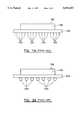
- FIG. 1Ais a schematic elevational view of a prior art Plastic Pin Grid Array integrated circuit package
- FIG. 1Bis a schematic plan view of the bottom of the package illustrated in FIG. 1A;
- FIG. 2Ais a schematic elevational view of a prior art Plastic Ball Grid Array integrated circuit package
- FIG. 2Bis a schematic plan view of the bottom of the package illustrated in FIG. 2A;
- FIG. 3is a schematic elevation sectional view of the packages of FIGS. 1A and 2A;
- FIG. 4is a schematic elevation sectional view of a preferred embodiment of the present invention.
- FIGS. 5A and 5Bare more detailed partial schematic elevational views of the invention of FIG. 4.
- FIG. 6is a schematic elevational view of another embodiment of the present invention.
- FIGS. 1A and 1Billustrate a prior art plastic pin grid array (PPGA) integrated circuit package.
- the PPGA package of FIGS. 1A and 1Bis comprised of a printed wiring board (PWB) 102, external connection pins 104, encapsulation 106, and lid 108.
- the pins 104may be mechanically connected to a system printed circuit board socket or soldered to plated through holes in the printed circuit board.
- the PWB 102has conductive traces (not illustrated) that connect the pins 104 to the electrical circuits on a semiconductor die (not illustrated) housed inside of the encapsulation 106.
- the lid 108covers the top of the encapsulation 106, and may be utilized as a planar surface for pick and place automatic assembly equipment.
- FIGS. 2A and 2Billustrate a prior art plastic ball grid array (PBGA) integrated circuit package.
- the PBGA package of FIGS. 2A and 2Bis comprised of a printed wiring board (PWB) 202, external connection solder balls 204, encapsulation 106, and lid 108.
- the solder balls 204are aligned with corresponding solder flux covered connection pads on a system printed circuit board, and when heated together, the solder balls 204 reflow to the connection pads on the printed circuit board (not illustrated).
- the PWB 202has conductive traces (not illustrated) that connect the solder balls 204 to the electrical circuits on a semiconductor die (not illustrated) housed inside of the encapsulation 106.
- the lid 108covers the top of the encapsulation 106, and may be utilized as a planar surface for pick and place automatic assembly equipment. The only significant difference between the PPGA and PBGA packages is the external connection pins and solder balls, respectively.
- FIG. 3a schematic elevation sectional view of the prior art packages of FIGS. 1A and 2A is illustrated.
- the pins 104 of FIG. 1A or solder balls 204 of FIG. 2Aare not illustrated for simplification and clarity.
- the encapsulation 106is comprised of a dam ring 302 which holds encapsulation material 304 around a semiconductor die 306 and bond wires 308.
- the encapsulation materialmay be "HYSOL" or any other type of encapsulation material known to those skilled in the art of semiconductor packaging.
- the semiconductor dieis electrically connected to conductive traces (not illustrated) on the PWB 102 by means of the bond wires 308.
- the encapsulation material 304entirely covers the semiconductor die 306, bond wires 308, and part of the surface of PWB 102.
- the encapsulation material 304is poured in a liquid form over the die 306 and the bond wires 308, then the encapsulation material is cured from a liquid to a solid.
- the encapsulation material 304may shrink while curing.
- the encapsulation material 304attaches to the surface of the PWB 102, and if the material 304 shrinks, then the PWB 102 may tend to bow. Bowing is undesirable because the lid 108 will not fit properly over the encapsulation material, or if the lid is placed on the dam ring 302 before the encapsulation material 304 cures, the lid 108 may also bow and lose its planarity. If the lid 108 loses its planarity, then the package may not be suitable for automatic pick and place assembly.
- the integrated circuit packageis comprised of the PWB 102, the semiconductor die 306 connected to conductive lands (not illustrated) on the PWB 102 by bond wires 308 metal pins 418 connect to the conductive lands, a planar substrate 410 is attached to the semiconductor die 306 by adhesive 412, and encapsulation materials 404a and 404b covers the bondwires 308, and connections to the die 306 and PWB 102.
- external heat sink 414may be attached to and in thermal communication with an exterior planar face 416 of the planar substrate 410.
- the adhesive 412may be filled with fused quartz (silica) particles 520 for improved thermal conductivity.
- the fused quartz particles 520allow a thicker adhesive 412 to still be thermally conductive while remaining an electrical insulator.
- a thin or thick layer of adhesive 412may be utilized without substantial degradation of heat transfer from the die 306 to the substrate 410.
- the planar substrate 410may be made of silicon, ceramic, metal or other materials having relative stiffness.
- the planar substrate 410will have substantially the same TCE as the die 306 so that over a large temperature range, the possibility of the planar substrate 410 causing the die 306 to warp is minimized.
- a compliant adhesivemay be utilized.
- the planar substrate 410may be composed of silicon, the same material as the die 306.
- a ready source of silicon planar substratesis from defective silicon wafers that did not pass fabrication testing. Normally these defective silicon wafers are thrown away as scrap, but the present invention may utilize these defective wafers by cutting them up as required for the planar substrates 410.
- the planar substrate 410 and die 306may also be attached together with an insulator 524 having adhesives 522a and 522b on its faces.
- the insulator 524may be, for example, a thin layer of polyimide.
- the adhesives 522a and 522bmay be B-staged epoxy.
- the bond wires 308are attached to bond pads 526 on the active face of the semiconductor die 306.
- the other ends of the bond wires 308are attached to conductive lands (not illustrated) on the PWB 102, as is well known to those skilled in the art of semiconductor package fabrication.
- Other methods for connecting a semiconductor device to a PWBare equally well known to those skilled in the art of semiconductor packaging, such as, for example, TAB, thermal compression bonding (internal leadframe), ball bonding, collapsible solder ball flip-chips, etc.
- the integrated circuit packageis comprised of the PWB 102, a flip-chip semiconductor die 606, collapsible solder balls 608 which connect the electrical circuits of the die 606 to conductive lands (not illustrated) on the PWB 102, solder balls 618 connect to the conductive land (conductive epoxy may be used in place of the solder balls with equally good results), and encapsulation materials 604a and 604b.
- an external heat sink 614may be attached to and in thermal communication with an exterior planar face 616 of the flip-chip die 606.
- the conductive lands of the PWB 102connect to external connection means (not illustrated for clarity) as mentioned above.
- the present inventionintroduces a new system and method of reducing the possibility of warpage in the fabrication of semiconductor integrated circuit packages, and reduces the cost and complexity of fabricating the semiconductor packages.
- a planar exterior surfacefacilitates the use of automatic pick and place assembly machines, and further provides an advantageous place to attach an external heat sink for improved thermal performance.
Landscapes
- Engineering & Computer Science (AREA)
- Microelectronics & Electronic Packaging (AREA)
- Computer Hardware Design (AREA)
- Power Engineering (AREA)
- Physics & Mathematics (AREA)
- Condensed Matter Physics & Semiconductors (AREA)
- General Physics & Mathematics (AREA)
- Cooling Or The Like Of Semiconductors Or Solid State Devices (AREA)
Abstract
Description
Claims (26)
Priority Applications (1)
| Application Number | Priority Date | Filing Date | Title |
|---|---|---|---|
| US08/412,087US5610442A (en) | 1995-03-27 | 1995-03-27 | Semiconductor device package fabrication method and apparatus |
Applications Claiming Priority (1)
| Application Number | Priority Date | Filing Date | Title |
|---|---|---|---|
| US08/412,087US5610442A (en) | 1995-03-27 | 1995-03-27 | Semiconductor device package fabrication method and apparatus |
Publications (1)
| Publication Number | Publication Date |
|---|---|
| US5610442Atrue US5610442A (en) | 1997-03-11 |
Family
ID=23631559
Family Applications (1)
| Application Number | Title | Priority Date | Filing Date |
|---|---|---|---|
| US08/412,087Expired - LifetimeUS5610442A (en) | 1995-03-27 | 1995-03-27 | Semiconductor device package fabrication method and apparatus |
Country Status (1)
| Country | Link |
|---|---|
| US (1) | US5610442A (en) |
Cited By (56)
| Publication number | Priority date | Publication date | Assignee | Title |
|---|---|---|---|---|
| US5789813A (en)* | 1996-09-30 | 1998-08-04 | Lsi Logic Corporation | Ball grid array package with inexpensive threaded secure locking mechanism to allow removal of a threaded heat sink therefrom |
| WO1998050949A3 (en)* | 1997-05-07 | 1999-02-04 | Lsi Logic Corp | Pbga stiffener package and method of manufacturing |
| US5891753A (en)* | 1997-01-24 | 1999-04-06 | Micron Technology, Inc. | Method and apparatus for packaging flip chip bare die on printed circuit boards |
| US5894166A (en)* | 1997-09-17 | 1999-04-13 | Northern Telecom Limited | Chip mounting scheme |
| US5895972A (en)* | 1996-12-31 | 1999-04-20 | Intel Corporation | Method and apparatus for cooling the backside of a semiconductor device using an infrared transparent heat slug |
| US5898571A (en)* | 1997-04-28 | 1999-04-27 | Lsi Logic Corporation | Apparatus and method for clip-on attachment of heat sinks to encapsulated semiconductor packages |
| US5900675A (en)* | 1997-04-21 | 1999-05-04 | International Business Machines Corporation | Organic controlled collapse chip connector (C4) ball grid array (BGA) chip carrier with dual thermal expansion rates |
| US5905301A (en)* | 1996-02-01 | 1999-05-18 | Nec Corporation | Mold package for sealing a chip |
| US5949142A (en)* | 1997-03-27 | 1999-09-07 | Kabushiki Kaisha Toshiba | Chip size package and method of manufacturing the same |
| US5977622A (en)* | 1997-04-25 | 1999-11-02 | Lsi Logic Corporation | Stiffener with slots for clip-on heat sink attachment |
| US6091603A (en)* | 1999-09-30 | 2000-07-18 | International Business Machines Corporation | Customizable lid for improved thermal performance of modules using flip chips |
| US6118177A (en)* | 1998-11-17 | 2000-09-12 | Lucent Technologies, Inc. | Heatspreader for a flip chip device, and method for connecting the heatspreader |
| US6117797A (en)* | 1998-09-03 | 2000-09-12 | Micron Technology, Inc. | Attachment method for heat sinks and devices involving removal of misplaced encapsulant |
| US6131278A (en)* | 1995-01-25 | 2000-10-17 | International Business Machines Corporation | Metal substrate having an IC chip and carrier mounting |
| US6173883B1 (en)* | 1998-11-17 | 2001-01-16 | Motorola, Inc. | Method and apparatus for increasing heat transfer that is restricted in thermally isolated pockets of a medium |
| US6208519B1 (en)* | 1999-08-31 | 2001-03-27 | Micron Technology, Inc. | Thermally enhanced semiconductor package |
| US6236568B1 (en)* | 1999-03-20 | 2001-05-22 | Siliconware Precision Industries, Co., Ltd. | Heat-dissipating structure for integrated circuit package |
| US6292369B1 (en) | 2000-08-07 | 2001-09-18 | International Business Machines Corporation | Methods for customizing lid for improved thermal performance of modules using flip chips |
| US6421248B1 (en)* | 1997-01-15 | 2002-07-16 | Infineon Technologies Ag | Chip card module |
| US6441499B1 (en)* | 2000-08-30 | 2002-08-27 | Lsi Logic Corporation | Thin form factor flip chip ball grid array |
| US6462405B1 (en)* | 2000-09-13 | 2002-10-08 | Siliconware Precision Industries Co., Ltd. | Semiconductor package |
| US6476502B2 (en)* | 1999-07-28 | 2002-11-05 | Mitsubishi Denki Kabushiki Kaisha | Semiconductor device and manufacturing method thereof |
| US6537400B1 (en) | 2000-03-06 | 2003-03-25 | Micron Technology, Inc. | Automated method of attaching flip chip devices to a substrate |
| US6555412B1 (en) | 1999-12-10 | 2003-04-29 | Micron Technology, Inc. | Packaged semiconductor chip and method of making same |
| US6570247B1 (en) | 1997-12-30 | 2003-05-27 | Intel Corporation | Integrated circuit device having an embedded heat slug |
| US6597065B1 (en)* | 2000-11-03 | 2003-07-22 | Texas Instruments Incorporated | Thermally enhanced semiconductor chip having integrated bonds over active circuits |
| US6737755B1 (en)* | 2002-07-19 | 2004-05-18 | Asat, Ltd. | Ball grid array package with improved thermal characteristics |
| US20040124545A1 (en)* | 1996-12-09 | 2004-07-01 | Daniel Wang | High density integrated circuits and the method of packaging the same |
| US20040196635A1 (en)* | 2002-11-20 | 2004-10-07 | Hee-Jin Park | Stacked chip package with heat transfer wires |
| US20040218363A1 (en)* | 2003-04-30 | 2004-11-04 | Wong Marvin Glenn | Application specific heat-dissipating apparatus that provides electrical isolation for components |
| US20040251957A1 (en)* | 2003-06-10 | 2004-12-16 | Do Chang Ho | Internal voltage generator |
| US6867499B1 (en) | 1999-09-30 | 2005-03-15 | Skyworks Solutions, Inc. | Semiconductor packaging |
| US6933176B1 (en) | 2002-07-19 | 2005-08-23 | Asat Ltd. | Ball grid array package and process for manufacturing same |
| US20050189646A1 (en)* | 1996-05-24 | 2005-09-01 | Salman Akram | Packaged die on PCB with heat sink encapsulant and methods |
| US20050224957A1 (en)* | 2004-01-28 | 2005-10-13 | Jeong-Woo Seo | Semiconductor package with heat dissipating structure and method of manufacturing the same |
| US6979594B1 (en) | 2002-07-19 | 2005-12-27 | Asat Ltd. | Process for manufacturing ball grid array package |
| US20060063300A1 (en)* | 2004-09-22 | 2006-03-23 | Tsorng-Dih Yuan | Structural design for flip-chip assembly |
| US7091581B1 (en) | 2004-06-14 | 2006-08-15 | Asat Limited | Integrated circuit package and process for fabricating the same |
| US20070040269A1 (en)* | 2005-08-22 | 2007-02-22 | Taiwan Semiconductor Manufacturing Co., Ltd. | Thermally enhanced cavity down ball grid array package |
| US20070205474A1 (en)* | 2006-03-02 | 2007-09-06 | Alps Electric Co., Ltd. | Pressure sensor having gold-silicon eutectic crystal layer interposed between contact layer and silicon substrate |
| US20070230115A1 (en)* | 2006-02-16 | 2007-10-04 | Stephan Dobritz | Memory module |
| US20080042262A1 (en)* | 2006-08-16 | 2008-02-21 | Crispell Robert B | Plastic overmolded packages with mechanically decoupled lid attach attachment |
| US20080068042A1 (en)* | 2004-11-04 | 2008-03-20 | Steven Teig | Programmable system in package |
| US7372151B1 (en) | 2003-09-12 | 2008-05-13 | Asat Ltd. | Ball grid array package and process for manufacturing same |
| US7411289B1 (en) | 2004-06-14 | 2008-08-12 | Asat Ltd. | Integrated circuit package with partially exposed contact pads and process for fabricating the same |
| US20100136423A1 (en)* | 2008-12-03 | 2010-06-03 | Kyungwon Seo | Secondary battery |
| DE102010041261A1 (en) | 2010-09-23 | 2012-03-29 | Robert Bosch Gmbh | Flip-chip arrangement with a cooling element and method for producing a flip-chip arrangement |
| US8201124B1 (en) | 2005-03-15 | 2012-06-12 | Tabula, Inc. | System in package and method of creating system in package |
| US20130313698A1 (en)* | 2012-05-24 | 2013-11-28 | Mediatek Inc. | Semiconductor package |
| US8610262B1 (en) | 2005-02-18 | 2013-12-17 | Utac Hong Kong Limited | Ball grid array package with improved thermal characteristics |
| US20150137343A1 (en)* | 2000-12-22 | 2015-05-21 | Broadcom Corporation | Enhanced die-up ball grid array and method for making the same |
| US9252068B2 (en) | 2012-05-24 | 2016-02-02 | Mediatek Inc. | Semiconductor package |
| CN110223961A (en)* | 2018-03-02 | 2019-09-10 | 美光科技公司 | Electronic device and associated system, device and method with package level heat regulator mechanism |
| US20200168525A1 (en)* | 2006-04-27 | 2020-05-28 | International Business Machines Corporation | Integrated circuit chip packaging |
| US11322456B2 (en)* | 2017-06-30 | 2022-05-03 | Intel Corporation | Die back side structures for warpage control |
| US12283555B2 (en)* | 2018-03-23 | 2025-04-22 | Analog Devices International Unlimited Company | Semiconductor packages |
Citations (8)
| Publication number | Priority date | Publication date | Assignee | Title |
|---|---|---|---|---|
| US4092697A (en)* | 1976-12-06 | 1978-05-30 | International Business Machines Corporation | Heat transfer mechanism for integrated circuit package |
| JPS62145751A (en)* | 1985-12-19 | 1987-06-29 | Mitsubishi Electric Corp | semiconductor equipment |
| US5157478A (en)* | 1989-04-19 | 1992-10-20 | Mitsubishi Denki Kabushiki Kaisha | Tape automated bonding packaged semiconductor device incorporating a heat sink |
| JPH06132425A (en)* | 1992-10-22 | 1994-05-13 | Kyocera Corp | Semiconductor device |
| US5357672A (en)* | 1993-08-13 | 1994-10-25 | Lsi Logic Corporation | Method and system for fabricating IC packages from laminated boards and heat spreader |
| US5438478A (en)* | 1992-10-20 | 1995-08-01 | Ibiden Co., Ltd. | Electronic component carriers and method of producing the same as well as electronic devices |
| US5455457A (en)* | 1990-11-27 | 1995-10-03 | Nec Corporation | Package for semiconductor elements having thermal dissipation means |
| EP0848180A1 (en)* | 1996-12-16 | 1998-06-17 | Ogura Clutch Co., Ltd. | Electromagnetic coupling device |
- 1995
- 1995-03-27USUS08/412,087patent/US5610442A/ennot_activeExpired - Lifetime
Patent Citations (8)
| Publication number | Priority date | Publication date | Assignee | Title |
|---|---|---|---|---|
| US4092697A (en)* | 1976-12-06 | 1978-05-30 | International Business Machines Corporation | Heat transfer mechanism for integrated circuit package |
| JPS62145751A (en)* | 1985-12-19 | 1987-06-29 | Mitsubishi Electric Corp | semiconductor equipment |
| US5157478A (en)* | 1989-04-19 | 1992-10-20 | Mitsubishi Denki Kabushiki Kaisha | Tape automated bonding packaged semiconductor device incorporating a heat sink |
| US5455457A (en)* | 1990-11-27 | 1995-10-03 | Nec Corporation | Package for semiconductor elements having thermal dissipation means |
| US5438478A (en)* | 1992-10-20 | 1995-08-01 | Ibiden Co., Ltd. | Electronic component carriers and method of producing the same as well as electronic devices |
| JPH06132425A (en)* | 1992-10-22 | 1994-05-13 | Kyocera Corp | Semiconductor device |
| US5357672A (en)* | 1993-08-13 | 1994-10-25 | Lsi Logic Corporation | Method and system for fabricating IC packages from laminated boards and heat spreader |
| EP0848180A1 (en)* | 1996-12-16 | 1998-06-17 | Ogura Clutch Co., Ltd. | Electromagnetic coupling device |
Non-Patent Citations (2)
| Title |
|---|
| "Electronic Packaging & Interconnection Handbook", pp. 7.24-7.27, C. Harper. |
| Electronic Packaging & Interconnection Handbook , pp. 7.24 7.27, C. Harper.* |
Cited By (100)
| Publication number | Priority date | Publication date | Assignee | Title |
|---|---|---|---|---|
| US6131278A (en)* | 1995-01-25 | 2000-10-17 | International Business Machines Corporation | Metal substrate having an IC chip and carrier mounting |
| US6150716A (en)* | 1995-01-25 | 2000-11-21 | International Business Machines Corporation | Metal substrate having an IC chip and carrier mounting |
| US5905301A (en)* | 1996-02-01 | 1999-05-18 | Nec Corporation | Mold package for sealing a chip |
| AU736114B2 (en)* | 1996-02-01 | 2001-07-26 | Renesas Electronics Corporation | Package |
| US20050189646A1 (en)* | 1996-05-24 | 2005-09-01 | Salman Akram | Packaged die on PCB with heat sink encapsulant and methods |
| US20070069372A1 (en)* | 1996-05-24 | 2007-03-29 | Salman Akram | Packaged die on PCB with heat sink encapsulant and methods |
| US5885848A (en)* | 1996-09-30 | 1999-03-23 | Lsi Logic Corporation | Ball grid array with inexpensive threaded secure locking mechanism to allow removal of a threaded heat sink therefrom |
| US5789813A (en)* | 1996-09-30 | 1998-08-04 | Lsi Logic Corporation | Ball grid array package with inexpensive threaded secure locking mechanism to allow removal of a threaded heat sink therefrom |
| US20040124545A1 (en)* | 1996-12-09 | 2004-07-01 | Daniel Wang | High density integrated circuits and the method of packaging the same |
| US5895972A (en)* | 1996-12-31 | 1999-04-20 | Intel Corporation | Method and apparatus for cooling the backside of a semiconductor device using an infrared transparent heat slug |
| US6251706B1 (en) | 1996-12-31 | 2001-06-26 | Intel Corporation | Method for cooling the backside of a semiconductor device using an infrared transparent heat slug |
| US6421248B1 (en)* | 1997-01-15 | 2002-07-16 | Infineon Technologies Ag | Chip card module |
| US6400032B1 (en) | 1997-01-24 | 2002-06-04 | Micron Technology, Inc. | Method and apparatus for packaging flip chip bare die on printed circuit boards |
| US6661103B2 (en) | 1997-01-24 | 2003-12-09 | Micron Technology, Inc. | Apparatus for packaging flip chip bare die on printed circuit boards |
| US5891753A (en)* | 1997-01-24 | 1999-04-06 | Micron Technology, Inc. | Method and apparatus for packaging flip chip bare die on printed circuit boards |
| US5949142A (en)* | 1997-03-27 | 1999-09-07 | Kabushiki Kaisha Toshiba | Chip size package and method of manufacturing the same |
| US5900675A (en)* | 1997-04-21 | 1999-05-04 | International Business Machines Corporation | Organic controlled collapse chip connector (C4) ball grid array (BGA) chip carrier with dual thermal expansion rates |
| US5977622A (en)* | 1997-04-25 | 1999-11-02 | Lsi Logic Corporation | Stiffener with slots for clip-on heat sink attachment |
| US5898571A (en)* | 1997-04-28 | 1999-04-27 | Lsi Logic Corporation | Apparatus and method for clip-on attachment of heat sinks to encapsulated semiconductor packages |
| US5972738A (en)* | 1997-05-07 | 1999-10-26 | Lsi Logic Corporation | PBGA stiffener package |
| WO1998050949A3 (en)* | 1997-05-07 | 1999-02-04 | Lsi Logic Corp | Pbga stiffener package and method of manufacturing |
| US5894166A (en)* | 1997-09-17 | 1999-04-13 | Northern Telecom Limited | Chip mounting scheme |
| US6607928B1 (en) | 1997-12-30 | 2003-08-19 | Intel Corporation | Integrated circuit device having an embedded heat slug |
| US6570247B1 (en) | 1997-12-30 | 2003-05-27 | Intel Corporation | Integrated circuit device having an embedded heat slug |
| US7244637B2 (en) | 1998-09-03 | 2007-07-17 | Micron Technology, Inc. | Chip on board and heat sink attachment methods |
| US6784113B2 (en) | 1998-09-03 | 2004-08-31 | Micron Technology, Inc. | Chip on board and heat sink attachment methods |
| US6432840B1 (en) | 1998-09-03 | 2002-08-13 | Micron Technology, Inc. | Methodology of removing misplaced encapsulant for attachment of heat sinks in a chip on board package |
| US6806567B2 (en)* | 1998-09-03 | 2004-10-19 | Micron Technology, Inc. | Chip on board with heat sink attachment and assembly |
| US6451709B1 (en) | 1998-09-03 | 2002-09-17 | Micron Technology, Inc. | Methodology of removing misplaced encapsulant for attachment of heat sinks in a chip on board package |
| US20040126931A1 (en)* | 1998-09-03 | 2004-07-01 | Hembree David R. | Chip on board and heat sink attachment methods |
| US6229204B1 (en) | 1998-09-03 | 2001-05-08 | Micron Technology, Inc. | Chip on board with heat sink attachment |
| US6630371B2 (en) | 1998-09-03 | 2003-10-07 | Micron Technology, Inc. | Chip on board and heat sink attachment methods |
| US6117797A (en)* | 1998-09-03 | 2000-09-12 | Micron Technology, Inc. | Attachment method for heat sinks and devices involving removal of misplaced encapsulant |
| US6596565B1 (en) | 1998-09-03 | 2003-07-22 | Micron Technology, Inc. | Chip on board and heat sink attachment methods |
| US6681482B1 (en) | 1998-11-17 | 2004-01-27 | Agere Systems, Inc. | Heatspreader for a flip chip device, and method for connecting the heatspreader |
| US6118177A (en)* | 1998-11-17 | 2000-09-12 | Lucent Technologies, Inc. | Heatspreader for a flip chip device, and method for connecting the heatspreader |
| US6173883B1 (en)* | 1998-11-17 | 2001-01-16 | Motorola, Inc. | Method and apparatus for increasing heat transfer that is restricted in thermally isolated pockets of a medium |
| US6236568B1 (en)* | 1999-03-20 | 2001-05-22 | Siliconware Precision Industries, Co., Ltd. | Heat-dissipating structure for integrated circuit package |
| US6476502B2 (en)* | 1999-07-28 | 2002-11-05 | Mitsubishi Denki Kabushiki Kaisha | Semiconductor device and manufacturing method thereof |
| US6601294B1 (en)* | 1999-08-31 | 2003-08-05 | Micron Technology, Inc. | Method for making a packaged semiconductor device |
| US6208519B1 (en)* | 1999-08-31 | 2001-03-27 | Micron Technology, Inc. | Thermally enhanced semiconductor package |
| US20050124232A1 (en)* | 1999-09-30 | 2005-06-09 | Behnam Tabrizi | Semiconductor packaging |
| US6091603A (en)* | 1999-09-30 | 2000-07-18 | International Business Machines Corporation | Customizable lid for improved thermal performance of modules using flip chips |
| US6867499B1 (en) | 1999-09-30 | 2005-03-15 | Skyworks Solutions, Inc. | Semiconductor packaging |
| US7192810B2 (en) | 1999-09-30 | 2007-03-20 | Skyworks Solutions, Inc. | Semiconductor packaging |
| US6555412B1 (en) | 1999-12-10 | 2003-04-29 | Micron Technology, Inc. | Packaged semiconductor chip and method of making same |
| US6773523B2 (en) | 2000-03-06 | 2004-08-10 | Micron Technology, Inc. | Automated method of attaching flip chip devices to a substrate |
| US6793749B2 (en) | 2000-03-06 | 2004-09-21 | Micron Technology, Inc. | Automated method of attaching flip-chip devices to a substrate |
| US6537400B1 (en) | 2000-03-06 | 2003-03-25 | Micron Technology, Inc. | Automated method of attaching flip chip devices to a substrate |
| US6292369B1 (en) | 2000-08-07 | 2001-09-18 | International Business Machines Corporation | Methods for customizing lid for improved thermal performance of modules using flip chips |
| US6441499B1 (en)* | 2000-08-30 | 2002-08-27 | Lsi Logic Corporation | Thin form factor flip chip ball grid array |
| US6462405B1 (en)* | 2000-09-13 | 2002-10-08 | Siliconware Precision Industries Co., Ltd. | Semiconductor package |
| US6784539B2 (en) | 2000-11-03 | 2004-08-31 | Texas Instruments Incorporated | Thermally enhanced semiconductor chip having integrated bonds over active circuits |
| US6597065B1 (en)* | 2000-11-03 | 2003-07-22 | Texas Instruments Incorporated | Thermally enhanced semiconductor chip having integrated bonds over active circuits |
| US20040004282A1 (en)* | 2000-11-03 | 2004-01-08 | Efland Taylor R. | Thermally enhanced semiconductor chip having integrated bonds over active circuits |
| US20150137343A1 (en)* | 2000-12-22 | 2015-05-21 | Broadcom Corporation | Enhanced die-up ball grid array and method for making the same |
| US6800948B1 (en)* | 2002-07-19 | 2004-10-05 | Asat Ltd. | Ball grid array package |
| US20060223229A1 (en)* | 2002-07-19 | 2006-10-05 | Asat Ltd. | Ball grid array package and process for manufacturing same |
| US6933176B1 (en) | 2002-07-19 | 2005-08-23 | Asat Ltd. | Ball grid array package and process for manufacturing same |
| US6737755B1 (en)* | 2002-07-19 | 2004-05-18 | Asat, Ltd. | Ball grid array package with improved thermal characteristics |
| US6818472B1 (en)* | 2002-07-19 | 2004-11-16 | Asat Ltd. | Ball grid array package |
| US6979594B1 (en) | 2002-07-19 | 2005-12-27 | Asat Ltd. | Process for manufacturing ball grid array package |
| US6987032B1 (en) | 2002-07-19 | 2006-01-17 | Asat Ltd. | Ball grid array package and process for manufacturing same |
| US7371610B1 (en) | 2002-07-19 | 2008-05-13 | Asat Ltd. | Process for fabricating an integrated circuit package with reduced mold warping |
| US7315080B1 (en) | 2002-07-19 | 2008-01-01 | Asat Ltd. | Ball grid array package that includes a collapsible spacer for separating die adapter from a heat spreader |
| US6857470B2 (en)* | 2002-11-20 | 2005-02-22 | Samsung Electronics Co., Ltd. | Stacked chip package with heat transfer wires |
| US20040196635A1 (en)* | 2002-11-20 | 2004-10-07 | Hee-Jin Park | Stacked chip package with heat transfer wires |
| US20040218363A1 (en)* | 2003-04-30 | 2004-11-04 | Wong Marvin Glenn | Application specific heat-dissipating apparatus that provides electrical isolation for components |
| US20040251957A1 (en)* | 2003-06-10 | 2004-12-16 | Do Chang Ho | Internal voltage generator |
| US7372151B1 (en) | 2003-09-12 | 2008-05-13 | Asat Ltd. | Ball grid array package and process for manufacturing same |
| US20050224957A1 (en)* | 2004-01-28 | 2005-10-13 | Jeong-Woo Seo | Semiconductor package with heat dissipating structure and method of manufacturing the same |
| US7202561B2 (en)* | 2004-01-28 | 2007-04-10 | Samsung Electronics Co., Ltd. | Semiconductor package with heat dissipating structure and method of manufacturing the same |
| US7091581B1 (en) | 2004-06-14 | 2006-08-15 | Asat Limited | Integrated circuit package and process for fabricating the same |
| US7411289B1 (en) | 2004-06-14 | 2008-08-12 | Asat Ltd. | Integrated circuit package with partially exposed contact pads and process for fabricating the same |
| US20060063300A1 (en)* | 2004-09-22 | 2006-03-23 | Tsorng-Dih Yuan | Structural design for flip-chip assembly |
| US7138300B2 (en) | 2004-09-22 | 2006-11-21 | Taiwan Semiconductor Manufacturing Co., Ltd. | Structural design for flip-chip assembly |
| US8536713B2 (en) | 2004-11-04 | 2013-09-17 | Tabula, Inc. | System in package with heat sink |
| US20080068042A1 (en)* | 2004-11-04 | 2008-03-20 | Steven Teig | Programmable system in package |
| US7936074B2 (en)* | 2004-11-04 | 2011-05-03 | Tabula, Inc. | Programmable system in package |
| US8610262B1 (en) | 2005-02-18 | 2013-12-17 | Utac Hong Kong Limited | Ball grid array package with improved thermal characteristics |
| US8201124B1 (en) | 2005-03-15 | 2012-06-12 | Tabula, Inc. | System in package and method of creating system in package |
| US20070040269A1 (en)* | 2005-08-22 | 2007-02-22 | Taiwan Semiconductor Manufacturing Co., Ltd. | Thermally enhanced cavity down ball grid array package |
| US20070230115A1 (en)* | 2006-02-16 | 2007-10-04 | Stephan Dobritz | Memory module |
| US20070205474A1 (en)* | 2006-03-02 | 2007-09-06 | Alps Electric Co., Ltd. | Pressure sensor having gold-silicon eutectic crystal layer interposed between contact layer and silicon substrate |
| US20200168525A1 (en)* | 2006-04-27 | 2020-05-28 | International Business Machines Corporation | Integrated circuit chip packaging |
| US7423341B2 (en)* | 2006-08-16 | 2008-09-09 | Agere Systems Inc. | Plastic overmolded packages with mechanically decoupled lid attach attachment |
| US20080042262A1 (en)* | 2006-08-16 | 2008-02-21 | Crispell Robert B | Plastic overmolded packages with mechanically decoupled lid attach attachment |
| US8349488B2 (en) | 2008-12-03 | 2013-01-08 | Samsung Sdi Co., Ltd. | Secondary battery including a protective circuit board made of metal |
| EP2197071A1 (en)* | 2008-12-03 | 2010-06-16 | Samsung SDI Co., Ltd. | Secondary battery |
| US20100136423A1 (en)* | 2008-12-03 | 2010-06-03 | Kyungwon Seo | Secondary battery |
| DE102010041261A1 (en) | 2010-09-23 | 2012-03-29 | Robert Bosch Gmbh | Flip-chip arrangement with a cooling element and method for producing a flip-chip arrangement |
| WO2012038121A1 (en) | 2010-09-23 | 2012-03-29 | Robert Bosch Gmbh | Flip-chip assembly having a cooling element and method for producing a flip-chip assembly |
| US20130313698A1 (en)* | 2012-05-24 | 2013-11-28 | Mediatek Inc. | Semiconductor package |
| US9184107B2 (en) | 2012-05-24 | 2015-11-10 | Mediatek Inc. | Semiconductor package |
| US9252068B2 (en) | 2012-05-24 | 2016-02-02 | Mediatek Inc. | Semiconductor package |
| US9000581B2 (en)* | 2012-05-24 | 2015-04-07 | Mediatek Inc. | Semiconductor package |
| US11322456B2 (en)* | 2017-06-30 | 2022-05-03 | Intel Corporation | Die back side structures for warpage control |
| CN110223961A (en)* | 2018-03-02 | 2019-09-10 | 美光科技公司 | Electronic device and associated system, device and method with package level heat regulator mechanism |
| CN110223961B (en)* | 2018-03-02 | 2023-06-06 | 美光科技公司 | Electronic device with package-level thermal regulator mechanism and associated systems, devices, and methods |
| US12283555B2 (en)* | 2018-03-23 | 2025-04-22 | Analog Devices International Unlimited Company | Semiconductor packages |
Similar Documents
| Publication | Publication Date | Title |
|---|---|---|
| US5610442A (en) | Semiconductor device package fabrication method and apparatus | |
| US5397921A (en) | Tab grid array | |
| US8018076B2 (en) | Semiconductor device, semiconductor package for use therein, and manufacturing method thereof | |
| US6518089B2 (en) | Flip chip semiconductor device in a molded chip scale package (CSP) and method of assembly | |
| KR100694739B1 (en) | Ball grid array package with multiple power / ground planes | |
| US7138706B2 (en) | Semiconductor device and method for manufacturing the same | |
| US6791195B2 (en) | Semiconductor device and manufacturing method of the same | |
| KR100268205B1 (en) | Attaching heat sinks directly to flip chips and ceramic chip carriers | |
| KR970002140B1 (en) | Semiconductor device, packaging method and lead tape | |
| KR0169820B1 (en) | Chip scale package with metal wiring substrate | |
| US7605020B2 (en) | Semiconductor chip package | |
| JPH06209055A (en) | Thermally reinforced semiconductor device with its exposed rear and its manufacture | |
| US6894229B1 (en) | Mechanically enhanced package and method of making same | |
| KR19980032206A (en) | High Performance Multichip Module Package | |
| US7365439B2 (en) | Semiconductor device, semiconductor package for use therein, and manufacturing method thereof | |
| US5888849A (en) | Method for fabricating an electronic package | |
| US6373125B1 (en) | Chip scale package with direct attachment of chip to lead frame | |
| US6710434B1 (en) | Window-type semiconductor package and fabrication method thereof | |
| US20030214019A1 (en) | Packaging system for semiconductor devices | |
| JP2769296B2 (en) | Semiconductor die package and method of manufacturing the same | |
| KR100520443B1 (en) | Chip scale package and its manufacturing method | |
| KR0150392B1 (en) | Tab grid array | |
| JPH09275169A (en) | Semiconductor device mounting structure | |
| JPH06163760A (en) | Electronic-component mounting board provided with heat-dissipating slug | |
| JPH09275172A (en) | Semiconductor device and mounting structure thereof |
Legal Events
| Date | Code | Title | Description |
|---|---|---|---|
| AS | Assignment | Owner name:LSI LOGIC CORPORATION, CALIFORNIA Free format text:ASSIGNMENT OF ASSIGNORS INTEREST;ASSIGNORS:SCHNEIDER, MARK R.;TRABUCCO, ROBERT T.;REEL/FRAME:007484/0149 Effective date:19950310 | |
| STCF | Information on status: patent grant | Free format text:PATENTED CASE | |
| FPAY | Fee payment | Year of fee payment:4 | |
| FPAY | Fee payment | Year of fee payment:8 | |
| CC | Certificate of correction | ||
| FEPP | Fee payment procedure | Free format text:PAYER NUMBER DE-ASSIGNED (ORIGINAL EVENT CODE: RMPN); ENTITY STATUS OF PATENT OWNER: LARGE ENTITY Free format text:PAYOR NUMBER ASSIGNED (ORIGINAL EVENT CODE: ASPN); ENTITY STATUS OF PATENT OWNER: LARGE ENTITY | |
| FPAY | Fee payment | Year of fee payment:12 | |
| AS | Assignment | Owner name:DEUTSCHE BANK AG NEW YORK BRANCH, AS COLLATERAL AG Free format text:PATENT SECURITY AGREEMENT;ASSIGNORS:LSI CORPORATION;AGERE SYSTEMS LLC;REEL/FRAME:032856/0031 Effective date:20140506 | |
| AS | Assignment | Owner name:LSI CORPORATION, CALIFORNIA Free format text:CHANGE OF NAME;ASSIGNOR:LSI LOGIC CORPORATION;REEL/FRAME:033102/0270 Effective date:20070406 | |
| AS | Assignment | Owner name:AVAGO TECHNOLOGIES GENERAL IP (SINGAPORE) PTE. LTD Free format text:ASSIGNMENT OF ASSIGNORS INTEREST;ASSIGNOR:LSI CORPORATION;REEL/FRAME:035390/0388 Effective date:20140814 | |
| AS | Assignment | Owner name:LSI CORPORATION, CALIFORNIA Free format text:TERMINATION AND RELEASE OF SECURITY INTEREST IN PATENT RIGHTS (RELEASES RF 032856-0031);ASSIGNOR:DEUTSCHE BANK AG NEW YORK BRANCH, AS COLLATERAL AGENT;REEL/FRAME:037684/0039 Effective date:20160201 Owner name:AGERE SYSTEMS LLC, PENNSYLVANIA Free format text:TERMINATION AND RELEASE OF SECURITY INTEREST IN PATENT RIGHTS (RELEASES RF 032856-0031);ASSIGNOR:DEUTSCHE BANK AG NEW YORK BRANCH, AS COLLATERAL AGENT;REEL/FRAME:037684/0039 Effective date:20160201 | |
| AS | Assignment | Owner name:BELL SEMICONDUCTOR, LLC, ILLINOIS Free format text:ASSIGNMENT OF ASSIGNORS INTEREST;ASSIGNORS:AVAGO TECHNOLOGIES GENERAL IP (SINGAPORE) PTE. LTD.;BROADCOM CORPORATION;REEL/FRAME:044886/0766 Effective date:20171208 | |
| AS | Assignment | Owner name:CORTLAND CAPITAL MARKET SERVICES LLC, AS COLLATERA Free format text:SECURITY INTEREST;ASSIGNORS:HILCO PATENT ACQUISITION 56, LLC;BELL SEMICONDUCTOR, LLC;BELL NORTHERN RESEARCH, LLC;REEL/FRAME:045216/0020 Effective date:20180124 | |
| AS | Assignment | Owner name:BELL NORTHERN RESEARCH, LLC, ILLINOIS Free format text:RELEASE BY SECURED PARTY;ASSIGNOR:CORTLAND CAPITAL MARKET SERVICES LLC;REEL/FRAME:059723/0382 Effective date:20220401 Owner name:BELL SEMICONDUCTOR, LLC, ILLINOIS Free format text:RELEASE BY SECURED PARTY;ASSIGNOR:CORTLAND CAPITAL MARKET SERVICES LLC;REEL/FRAME:059723/0382 Effective date:20220401 Owner name:HILCO PATENT ACQUISITION 56, LLC, ILLINOIS Free format text:RELEASE BY SECURED PARTY;ASSIGNOR:CORTLAND CAPITAL MARKET SERVICES LLC;REEL/FRAME:059723/0382 Effective date:20220401 |