US5608264A - Surface mountable integrated circuit with conductive vias - Google Patents
Surface mountable integrated circuit with conductive viasDownload PDFInfo
- Publication number
- US5608264A US5608264AUS08/461,643US46164395AUS5608264AUS 5608264 AUS5608264 AUS 5608264AUS 46164395 AUS46164395 AUS 46164395AUS 5608264 AUS5608264 AUS 5608264A
- Authority
- US
- United States
- Prior art keywords
- wafer
- layer
- integrated circuit
- metal
- die
- Prior art date
- Legal status (The legal status is an assumption and is not a legal conclusion. Google has not performed a legal analysis and makes no representation as to the accuracy of the status listed.)
- Expired - Lifetime
Links
Images


Classifications
- H—ELECTRICITY
- H01—ELECTRIC ELEMENTS
- H01L—SEMICONDUCTOR DEVICES NOT COVERED BY CLASS H10
- H01L23/00—Details of semiconductor or other solid state devices
- H01L23/52—Arrangements for conducting electric current within the device in operation from one component to another, i.e. interconnections, e.g. wires, lead frames
- H01L23/522—Arrangements for conducting electric current within the device in operation from one component to another, i.e. interconnections, e.g. wires, lead frames including external interconnections consisting of a multilayer structure of conductive and insulating layers inseparably formed on the semiconductor body
- H01L23/532—Arrangements for conducting electric current within the device in operation from one component to another, i.e. interconnections, e.g. wires, lead frames including external interconnections consisting of a multilayer structure of conductive and insulating layers inseparably formed on the semiconductor body characterised by the materials
- H01L23/53204—Conductive materials
- H01L23/53209—Conductive materials based on metals, e.g. alloys, metal silicides
- H01L23/53257—Conductive materials based on metals, e.g. alloys, metal silicides the principal metal being a refractory metal
- H—ELECTRICITY
- H01—ELECTRIC ELEMENTS
- H01L—SEMICONDUCTOR DEVICES NOT COVERED BY CLASS H10
- H01L23/00—Details of semiconductor or other solid state devices
- H01L23/48—Arrangements for conducting electric current to or from the solid state body in operation, e.g. leads, terminal arrangements ; Selection of materials therefor
- H01L23/481—Internal lead connections, e.g. via connections, feedthrough structures
- H—ELECTRICITY
- H01—ELECTRIC ELEMENTS
- H01L—SEMICONDUCTOR DEVICES NOT COVERED BY CLASS H10
- H01L25/00—Assemblies consisting of a plurality of semiconductor or other solid state devices
- H01L25/03—Assemblies consisting of a plurality of semiconductor or other solid state devices all the devices being of a type provided for in a single subclass of subclasses H10B, H10D, H10F, H10H, H10K or H10N, e.g. assemblies of rectifier diodes
- H01L25/04—Assemblies consisting of a plurality of semiconductor or other solid state devices all the devices being of a type provided for in a single subclass of subclasses H10B, H10D, H10F, H10H, H10K or H10N, e.g. assemblies of rectifier diodes the devices not having separate containers
- H01L25/065—Assemblies consisting of a plurality of semiconductor or other solid state devices all the devices being of a type provided for in a single subclass of subclasses H10B, H10D, H10F, H10H, H10K or H10N, e.g. assemblies of rectifier diodes the devices not having separate containers the devices being of a type provided for in group H10D89/00
- H01L25/0657—Stacked arrangements of devices
- H—ELECTRICITY
- H01—ELECTRIC ELEMENTS
- H01L—SEMICONDUCTOR DEVICES NOT COVERED BY CLASS H10
- H01L2224/00—Indexing scheme for arrangements for connecting or disconnecting semiconductor or solid-state bodies and methods related thereto as covered by H01L24/00
- H01L2224/01—Means for bonding being attached to, or being formed on, the surface to be connected, e.g. chip-to-package, die-attach, "first-level" interconnects; Manufacturing methods related thereto
- H01L2224/42—Wire connectors; Manufacturing methods related thereto
- H01L2224/44—Structure, shape, material or disposition of the wire connectors prior to the connecting process
- H01L2224/45—Structure, shape, material or disposition of the wire connectors prior to the connecting process of an individual wire connector
- H01L2224/45001—Core members of the connector
- H01L2224/45099—Material
- H01L2224/451—Material with a principal constituent of the material being a metal or a metalloid, e.g. boron (B), silicon (Si), germanium (Ge), arsenic (As), antimony (Sb), tellurium (Te) and polonium (Po), and alloys thereof
- H—ELECTRICITY
- H01—ELECTRIC ELEMENTS
- H01L—SEMICONDUCTOR DEVICES NOT COVERED BY CLASS H10
- H01L2224/00—Indexing scheme for arrangements for connecting or disconnecting semiconductor or solid-state bodies and methods related thereto as covered by H01L24/00
- H01L2224/01—Means for bonding being attached to, or being formed on, the surface to be connected, e.g. chip-to-package, die-attach, "first-level" interconnects; Manufacturing methods related thereto
- H01L2224/42—Wire connectors; Manufacturing methods related thereto
- H01L2224/47—Structure, shape, material or disposition of the wire connectors after the connecting process
- H01L2224/48—Structure, shape, material or disposition of the wire connectors after the connecting process of an individual wire connector
- H01L2224/4805—Shape
- H01L2224/4809—Loop shape
- H01L2224/48091—Arched
- H—ELECTRICITY
- H01—ELECTRIC ELEMENTS
- H01L—SEMICONDUCTOR DEVICES NOT COVERED BY CLASS H10
- H01L2224/00—Indexing scheme for arrangements for connecting or disconnecting semiconductor or solid-state bodies and methods related thereto as covered by H01L24/00
- H01L2224/01—Means for bonding being attached to, or being formed on, the surface to be connected, e.g. chip-to-package, die-attach, "first-level" interconnects; Manufacturing methods related thereto
- H01L2224/42—Wire connectors; Manufacturing methods related thereto
- H01L2224/47—Structure, shape, material or disposition of the wire connectors after the connecting process
- H01L2224/48—Structure, shape, material or disposition of the wire connectors after the connecting process of an individual wire connector
- H01L2224/481—Disposition
- H01L2224/48151—Connecting between a semiconductor or solid-state body and an item not being a semiconductor or solid-state body, e.g. chip-to-substrate, chip-to-passive
- H01L2224/48221—Connecting between a semiconductor or solid-state body and an item not being a semiconductor or solid-state body, e.g. chip-to-substrate, chip-to-passive the body and the item being stacked
- H01L2224/48225—Connecting between a semiconductor or solid-state body and an item not being a semiconductor or solid-state body, e.g. chip-to-substrate, chip-to-passive the body and the item being stacked the item being non-metallic, e.g. insulating substrate with or without metallisation
- H01L2224/48227—Connecting between a semiconductor or solid-state body and an item not being a semiconductor or solid-state body, e.g. chip-to-substrate, chip-to-passive the body and the item being stacked the item being non-metallic, e.g. insulating substrate with or without metallisation connecting the wire to a bond pad of the item
- H—ELECTRICITY
- H01—ELECTRIC ELEMENTS
- H01L—SEMICONDUCTOR DEVICES NOT COVERED BY CLASS H10
- H01L2225/00—Details relating to assemblies covered by the group H01L25/00 but not provided for in its subgroups
- H01L2225/03—All the devices being of a type provided for in the same main group of the same subclass of class H10, e.g. assemblies of rectifier diodes
- H01L2225/04—All the devices being of a type provided for in the same main group of the same subclass of class H10, e.g. assemblies of rectifier diodes the devices not having separate containers
- H01L2225/065—All the devices being of a type provided for in the same main group of the same subclass of class H10
- H01L2225/06503—Stacked arrangements of devices
- H01L2225/06513—Bump or bump-like direct electrical connections between devices, e.g. flip-chip connection, solder bumps
- H—ELECTRICITY
- H01—ELECTRIC ELEMENTS
- H01L—SEMICONDUCTOR DEVICES NOT COVERED BY CLASS H10
- H01L2225/00—Details relating to assemblies covered by the group H01L25/00 but not provided for in its subgroups
- H01L2225/03—All the devices being of a type provided for in the same main group of the same subclass of class H10, e.g. assemblies of rectifier diodes
- H01L2225/04—All the devices being of a type provided for in the same main group of the same subclass of class H10, e.g. assemblies of rectifier diodes the devices not having separate containers
- H01L2225/065—All the devices being of a type provided for in the same main group of the same subclass of class H10
- H01L2225/06503—Stacked arrangements of devices
- H01L2225/06527—Special adaptation of electrical connections, e.g. rewiring, engineering changes, pressure contacts, layout
- H—ELECTRICITY
- H01—ELECTRIC ELEMENTS
- H01L—SEMICONDUCTOR DEVICES NOT COVERED BY CLASS H10
- H01L2225/00—Details relating to assemblies covered by the group H01L25/00 but not provided for in its subgroups
- H01L2225/03—All the devices being of a type provided for in the same main group of the same subclass of class H10, e.g. assemblies of rectifier diodes
- H01L2225/04—All the devices being of a type provided for in the same main group of the same subclass of class H10, e.g. assemblies of rectifier diodes the devices not having separate containers
- H01L2225/065—All the devices being of a type provided for in the same main group of the same subclass of class H10
- H01L2225/06503—Stacked arrangements of devices
- H01L2225/06541—Conductive via connections through the device, e.g. vertical interconnects, through silicon via [TSV]
- H—ELECTRICITY
- H01—ELECTRIC ELEMENTS
- H01L—SEMICONDUCTOR DEVICES NOT COVERED BY CLASS H10
- H01L2225/00—Details relating to assemblies covered by the group H01L25/00 but not provided for in its subgroups
- H01L2225/03—All the devices being of a type provided for in the same main group of the same subclass of class H10, e.g. assemblies of rectifier diodes
- H01L2225/04—All the devices being of a type provided for in the same main group of the same subclass of class H10, e.g. assemblies of rectifier diodes the devices not having separate containers
- H01L2225/065—All the devices being of a type provided for in the same main group of the same subclass of class H10
- H01L2225/06503—Stacked arrangements of devices
- H01L2225/06551—Conductive connections on the side of the device
- H—ELECTRICITY
- H01—ELECTRIC ELEMENTS
- H01L—SEMICONDUCTOR DEVICES NOT COVERED BY CLASS H10
- H01L2225/00—Details relating to assemblies covered by the group H01L25/00 but not provided for in its subgroups
- H01L2225/03—All the devices being of a type provided for in the same main group of the same subclass of class H10, e.g. assemblies of rectifier diodes
- H01L2225/04—All the devices being of a type provided for in the same main group of the same subclass of class H10, e.g. assemblies of rectifier diodes the devices not having separate containers
- H01L2225/065—All the devices being of a type provided for in the same main group of the same subclass of class H10
- H01L2225/06503—Stacked arrangements of devices
- H01L2225/06589—Thermal management, e.g. cooling
- H—ELECTRICITY
- H01—ELECTRIC ELEMENTS
- H01L—SEMICONDUCTOR DEVICES NOT COVERED BY CLASS H10
- H01L24/00—Arrangements for connecting or disconnecting semiconductor or solid-state bodies; Methods or apparatus related thereto
- H01L24/01—Means for bonding being attached to, or being formed on, the surface to be connected, e.g. chip-to-package, die-attach, "first-level" interconnects; Manufacturing methods related thereto
- H01L24/42—Wire connectors; Manufacturing methods related thereto
- H01L24/44—Structure, shape, material or disposition of the wire connectors prior to the connecting process
- H01L24/45—Structure, shape, material or disposition of the wire connectors prior to the connecting process of an individual wire connector
- H—ELECTRICITY
- H01—ELECTRIC ELEMENTS
- H01L—SEMICONDUCTOR DEVICES NOT COVERED BY CLASS H10
- H01L24/00—Arrangements for connecting or disconnecting semiconductor or solid-state bodies; Methods or apparatus related thereto
- H01L24/01—Means for bonding being attached to, or being formed on, the surface to be connected, e.g. chip-to-package, die-attach, "first-level" interconnects; Manufacturing methods related thereto
- H01L24/42—Wire connectors; Manufacturing methods related thereto
- H01L24/47—Structure, shape, material or disposition of the wire connectors after the connecting process
- H01L24/48—Structure, shape, material or disposition of the wire connectors after the connecting process of an individual wire connector
- H—ELECTRICITY
- H01—ELECTRIC ELEMENTS
- H01L—SEMICONDUCTOR DEVICES NOT COVERED BY CLASS H10
- H01L2924/00—Indexing scheme for arrangements or methods for connecting or disconnecting semiconductor or solid-state bodies as covered by H01L24/00
- H01L2924/01—Chemical elements
- H01L2924/01029—Copper [Cu]
- H—ELECTRICITY
- H01—ELECTRIC ELEMENTS
- H01L—SEMICONDUCTOR DEVICES NOT COVERED BY CLASS H10
- H01L2924/00—Indexing scheme for arrangements or methods for connecting or disconnecting semiconductor or solid-state bodies as covered by H01L24/00
- H01L2924/01—Chemical elements
- H01L2924/01046—Palladium [Pd]
- H—ELECTRICITY
- H01—ELECTRIC ELEMENTS
- H01L—SEMICONDUCTOR DEVICES NOT COVERED BY CLASS H10
- H01L2924/00—Indexing scheme for arrangements or methods for connecting or disconnecting semiconductor or solid-state bodies as covered by H01L24/00
- H01L2924/01—Chemical elements
- H01L2924/01078—Platinum [Pt]
- H—ELECTRICITY
- H01—ELECTRIC ELEMENTS
- H01L—SEMICONDUCTOR DEVICES NOT COVERED BY CLASS H10
- H01L2924/00—Indexing scheme for arrangements or methods for connecting or disconnecting semiconductor or solid-state bodies as covered by H01L24/00
- H01L2924/01—Chemical elements
- H01L2924/01079—Gold [Au]
- H—ELECTRICITY
- H01—ELECTRIC ELEMENTS
- H01L—SEMICONDUCTOR DEVICES NOT COVERED BY CLASS H10
- H01L2924/00—Indexing scheme for arrangements or methods for connecting or disconnecting semiconductor or solid-state bodies as covered by H01L24/00
- H01L2924/049—Nitrides composed of metals from groups of the periodic table
- H01L2924/0494—4th Group
- H01L2924/04941—TiN
- H—ELECTRICITY
- H01—ELECTRIC ELEMENTS
- H01L—SEMICONDUCTOR DEVICES NOT COVERED BY CLASS H10
- H01L2924/00—Indexing scheme for arrangements or methods for connecting or disconnecting semiconductor or solid-state bodies as covered by H01L24/00
- H01L2924/10—Details of semiconductor or other solid state devices to be connected
- H01L2924/102—Material of the semiconductor or solid state bodies
- H01L2924/1025—Semiconducting materials
- H01L2924/10251—Elemental semiconductors, i.e. Group IV
- H01L2924/10253—Silicon [Si]
- H—ELECTRICITY
- H01—ELECTRIC ELEMENTS
- H01L—SEMICONDUCTOR DEVICES NOT COVERED BY CLASS H10
- H01L2924/00—Indexing scheme for arrangements or methods for connecting or disconnecting semiconductor or solid-state bodies as covered by H01L24/00
- H01L2924/10—Details of semiconductor or other solid state devices to be connected
- H01L2924/11—Device type
- H01L2924/12—Passive devices, e.g. 2 terminal devices
- H01L2924/1204—Optical Diode
- H01L2924/12041—LED
- H—ELECTRICITY
- H01—ELECTRIC ELEMENTS
- H01L—SEMICONDUCTOR DEVICES NOT COVERED BY CLASS H10
- H01L2924/00—Indexing scheme for arrangements or methods for connecting or disconnecting semiconductor or solid-state bodies as covered by H01L24/00
- H01L2924/10—Details of semiconductor or other solid state devices to be connected
- H01L2924/11—Device type
- H01L2924/12—Passive devices, e.g. 2 terminal devices
- H01L2924/1204—Optical Diode
- H01L2924/12042—LASER
- H—ELECTRICITY
- H01—ELECTRIC ELEMENTS
- H01L—SEMICONDUCTOR DEVICES NOT COVERED BY CLASS H10
- H01L2924/00—Indexing scheme for arrangements or methods for connecting or disconnecting semiconductor or solid-state bodies as covered by H01L24/00
- H01L2924/10—Details of semiconductor or other solid state devices to be connected
- H01L2924/11—Device type
- H01L2924/12—Passive devices, e.g. 2 terminal devices
- H01L2924/1204—Optical Diode
- H01L2924/12043—Photo diode
- H—ELECTRICITY
- H01—ELECTRIC ELEMENTS
- H01L—SEMICONDUCTOR DEVICES NOT COVERED BY CLASS H10
- H01L2924/00—Indexing scheme for arrangements or methods for connecting or disconnecting semiconductor or solid-state bodies as covered by H01L24/00
- H01L2924/10—Details of semiconductor or other solid state devices to be connected
- H01L2924/11—Device type
- H01L2924/14—Integrated circuits
- H—ELECTRICITY
- H01—ELECTRIC ELEMENTS
- H01L—SEMICONDUCTOR DEVICES NOT COVERED BY CLASS H10
- H01L2924/00—Indexing scheme for arrangements or methods for connecting or disconnecting semiconductor or solid-state bodies as covered by H01L24/00
- H01L2924/15—Details of package parts other than the semiconductor or other solid state devices to be connected
- H01L2924/151—Die mounting substrate
- H01L2924/1517—Multilayer substrate
- H01L2924/15182—Fan-in arrangement of the internal vias
- H01L2924/15184—Fan-in arrangement of the internal vias in different layers of the multilayer substrate
- H—ELECTRICITY
- H01—ELECTRIC ELEMENTS
- H01L—SEMICONDUCTOR DEVICES NOT COVERED BY CLASS H10
- H01L2924/00—Indexing scheme for arrangements or methods for connecting or disconnecting semiconductor or solid-state bodies as covered by H01L24/00
- H01L2924/15—Details of package parts other than the semiconductor or other solid state devices to be connected
- H01L2924/161—Cap
- H01L2924/1615—Shape
- H01L2924/16195—Flat cap [not enclosing an internal cavity]
- H—ELECTRICITY
- H01—ELECTRIC ELEMENTS
- H01L—SEMICONDUCTOR DEVICES NOT COVERED BY CLASS H10
- H01L2924/00—Indexing scheme for arrangements or methods for connecting or disconnecting semiconductor or solid-state bodies as covered by H01L24/00
- H01L2924/30—Technical effects
- H01L2924/301—Electrical effects
- H01L2924/3025—Electromagnetic shielding
Definitions
- Integrated circuitsare formed upon semiconductor substrates known as wafers.
- a waterholds a number of identical integrated circuits, each circuit being a die that is spaced from other identical circuits. Dies are separated from the wafer usually by a dicing operation. In the dicing operation wafers are mounted on an adhesive film and the water is placed in a diamond saw apparatus. The diamond saw apparatus cuts the wafer to separate the dies from each other.
- each dieis removed from the adhesive substrate and placed on a lead frame.
- a lead frameincludes a plurality of finger-like connections that extend from the periphery of the lead frame toward a center die pad.
- the dieis mounted on the center die pad.
- wire bondsare formed between bond pads on the die and the lead fingers of the lead frame.
- the individual dieare encapsulated in plastic during a molding operation.
- the lead frame with the attached diemay be mounted in a ceramic package which is then hermetically sealed.
- Still another alternativeis to directly mount the die onto a printed circuit board that contain other die which are interconnected to form an electronic system, such as a computer.
- solder-bump interconnectionOne technique for surface mounting dies on printed circuit boards uses a solder-bump interconnection. With that technique, the bond pads of the die have solder bumps or other wettable metal terminals deposited on the bond pads of the die. The die is mounted face side down onto a printed circuit board where the solder bumps of the die are aligned to electrical contacts on the board. In a typical application, the electrical contacts are metal lands that are recessed between raised glass walls. The solder-bump forms a collapsible wall of solder. The glass dam material helps retain the solder when the solder is heated.
- Such surface mountable techniquescan be used without packaging the die in protective plastic or ceramic encapsulating material. As such, surface mountable techniques reduce the number of steps in fabrication of electronic systems such as computers. However, one of the drawbacks with current surface mountable techniques is that the printed circuit board receives only a single layer of die.
- the inventionprovides a surface mountable integrated circuit and a method for fabricating surface mountable integrated circuits and for interconnecting surface mountable integrated circuits.
- the method of fabricationbegins with a wafer of semiconductor material having first and second surfaces. Integrated circuits are formed in the first surface of the wafer. Vias are formed in the wafer. The vias extend from an open end adjacent the first surface into the wafer. The vias terminate at a second, closed end that is a controlled distance from the second surface of the wafer. The via is filled with a conductive material. The second surface of the wafer is removed to expose the filling of the via above the reduced second surface.
- the side walls of the viaare coated with an insulating or dielectric material.
- a layer of metalis deposited on top of the insulating or dielectric material.
- the metalmay be deposited in two layers.
- a first layeris a barrier layer that will prevent migration of material into the via.
- a second or adhesion metalis deposited on the barrier metal.
- the adhesion metalsticks to both the barrier metal and to a third metal that fills the via.
- the third metalmay be selectively deposited tungsten.
- the inventionprovides for an integrated circuit die made of semiconductor material.
- the diehas first and second surfaces that are separated from each other by the body of semiconductor material.
- a conductive viaextends from one end at the first surface of the die to its second end that is a controlled distance from the second surface of the die.
- the viahas a layer of insulating or dielectric material on the wall of the via that is formed by the semiconductor material.
- the viais filled with a conductive material.
- the conductive materialmay be either metal or polysilicon.
- the viamay extend a predetermined or controlled length beyond the second surface of the die. As an alternative, the conductive material may terminate inside the via a controlled depth beneath the second surface of the die.
- the surface mountable integrated circuit of the inventionprovides for conductive vias in the form of prongs which extend from the second or back surface of the die as well as conductive vias in the form of receptacles where the conductive material is disposed a predetermined distance from the second surface of the die.
- the conductive material in the viamay be suitably formed to receive a corresponding prong from another die or substrate.
- diesmay be interconnected with each other or may be mounted on PC boards with suitable prongs or receptacles, as the case may be.
- a viamay include a prong, a receptacle, or both, with the prong at one end of the via and the receptacle at the other end of the via.
- the conductive material in the viasmay be metal or may be polysilicon.
- the conductive vias of the inventionmay also be formed in a single, bulk wafer of silicon.
- the conductive viasmay be formed in a bonded wafer that includes a device wafer bonded to a handle wafer by a suitable bonding layer such as a bonding oxide layer.
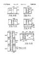
- FIGS. 1-1 to 1-11illustrate section views of an integrated circuit die processed according to a first embodiment of the invention.
- FIGS. 2-1 to 2-4show section views of an integrated circuit die processed according to a second embodiment of the invention.
- FIG. 3illustrates a section view of a third embodiment of the invention where a plurality of through vias are filled with metal which extends from the backside of the integrated circuit die.
- FIGS. 4-1 to 4-6show section views of an integrated circuit die processed according to a fourth embodiment of the invention.
- FIG. 4-7illustrates in perspective view an integrated circuit die which has a plurality of receptacles formed on its back surface. Also shown is a substrate with a plurality of interconnect pins which are spaced so as to plug into corresponding receptacles on the integrated circuit die.
- FIGS. 4-8 and 4-9show section views of two processing variants to the fourth embodiment. These section views correspond roughly to FIG. 4-2.
- FIGS. 4-10 to 4-14show section views of a seventh embodiment of the invention.
- FIG. 4-15illustrates a section view of a variation of the seventh embodiment of the invention.
- FIG. 5shows a section view of an eighth embodiment of the invention where multiple integrated circuit die are interconnected by stacking one die upon the next. Both electrical and optical interconnections are shown.
- FIG. 6illustrates a section view of a ninth embodiment of the invention in which a interposer is provided to furnish the contact metalization for the conductive through vias.
- FIG. 7illustrates a section view of a tenth embodiment of the invention in which a very thin integrated circuit die is stabilized and held rigid by a supportive layer applied to the frontside of the die.
- FIGS. 8-1 and 8-2show section and plan views, respectively, of an eleventh embodiment of the invention.
- FIG. 9-1shows a section view of a prior art multilayer ceramic package.
- FIG. 9-2shows a section view of a twelfth embodiment of the invention.
- FIG. 9-3illustrates a section view of a further embodiment of the stacked die illustrated in FIG. 4-15 and FIG. 5.
- FIGS. 10-1 to 10-11are a combination of section and plan views of integrated circuit dies illustrating a fourteenth embodiment of the invention where die edge connections are fabricated.
- FIGS. 10-12 and 10-13are section views showing alternative processing steps for the fourteenth embodiment.
- FIG. 10-14shows a perspective view of two dies fabricated in accordance with the fourteenth embodiment.
- the diesare connected to a substrate along three edges and connected to each other along the fourth edge.
- FIG. 10-15 and 10-16show perspective views of dies fabricated in accordance with the fourteenth embodiment which are mounted to a substrate in a perpendicular direction.
- a bonded wafer 110having a device wafer 111 bonded to a handle wafer 116 by a bonding layer 115.
- the device wafer 111is a wafer of monocrystalline silicon
- the handle waferis also made of silicon
- the bonding layer 115is a layer of silicon dioxide.
- the device wafer 111has one or more integrated circuit regions 119 formed in a first or upper surface 112.
- a second surface 113is spaced from the first surface 112 by the thickness of the device wafer 111, which may range from several 1000 ⁇ to 10 mils or greater in thickness.
- the handle wafer 116has a first handle surface 117 that faces the oxide bonding layer 115 and the second surface 113 of the device wafer 111.
- the second surface 118 of handle wafer 116is spaced from the first surface 117 by the thickness of the handle wafer 116.
- the integrated circuit regions 119are completed in so far as they are passivated with a surface oxide layer 114. In a preferred embodiment, integrated circuit devices are not yet interconnected with a metalization layer.
- a layer of photoresist 120is uniformly deposited over the oxide layer 114.
- the photoresist layer 120is patterned to define via openings 130.
- the via 130is suitably etched by using a plasma etch with a CF 4 or CHF 3 +O 2 chemistry, for example, to remove the exposed portion of the oxide layer 114 and a plasma etch with a NF 3 , HBr/Cl or SF 6 chemistry, for example, to remove the silicon in the device wafer 111.
- the via 130extends to or through the bond oxide layer 115 by again using an oxide plasma etch process, if necessary.
- the via 130has a first end 132 that is open on the first surface 112 of the device wafer 111.
- the viahas the side wall 131 that defines the length of its opening and has a second end 132.
- the second end 132 of the via 130terminates at a predetermined distance from the second surface 118 of the handle wafer 116.
- the photoresist 120is stripped and the side wall 131 and second end 132 of via 130 is deposited with the oxide layer 134.
- the oxide 134can be thermally grown, provided that the integrated circuit devices are not adversely affected by the additional high temperature processing, or deposited at low temperature using chemical vapor deposition (CVD).
- a barrier metal 135is then deposited on top of the oxide layer 134.
- barrier metal 135comprises titanium nitride (TIN) deposited using CVD to a thickness in the range of 100 to 1000 ⁇ . It may also be possible to deposit other barrier metals such as Cu, Pd, Pt or Ni using sputtering or evaporation provided the deposition method is capable of coating inside the via 130.
- an adhesion layer 136may also be needed.
- Typical adhesion metalsinclude chromium, titanium and titanium tungsten.
- the adhesion layer 136is deposited using sputtering or evaporation within the same constraints as previously discussed for barrier metals other than TiN. Both barrier and adhesion metals are deposited to a thickness of approximately 1000 ⁇ . In the preferred embodiment, a single layer of TiN functions as both a barrier metal and adhesion layer.
- barrier metal 135 and optional adhesion layer 136is followed by a step (see FIGS. 1-4) in which photoresist 140 is uniformly deposited on the surface of the device wafer 111 and fills all of the vias 130.
- the purpose of the photoresist 140 in the via 130is to protect the adhesion metal 135 and optional barrier metal 136 in the bottom of the via 130.
- the photoresistis a positive resist so that exposure to ultraviolet radiation will soften the resist.
- the resist 140is exposed to enough ultraviolet radiation to soften the resist to a predetermined depth D below the first surface 112 of the device wafer 111.
- the softened photoresist 141is then removed using a development process, and barrier metal 135 and optional adhesion layer 136 are etched leaving only those portions that are protected by the undeveloped photoresist 142 in the vias 130.
- the TiN barrier/adhesion layeris etched using a wet etch of dilute hydrofluoric acid or a dry etch using SF 6 or NF 3 chemistry.
- the undeveloped photoresist 142fills the lower portion of the via 130.
- the photoresist 142is then removed from via 130 and selectively deposited metal 137, e.g. tungsten, fills via 130 as shown in FIG. 1-6.
- the metal layer 137is deposited to the surface of the oxide 114.
- FIGS. 1-7 to 1-9An alternate processing sequence for the via refill is shown in FIGS. 1-7 to 1-9.
- This sequencecould be used where the via width is wider than can be reasonably filled using a single selective deposition of metal 137 as shown in FIG. 1-6 and where the via has a high aspect ratio; i.e. depth:width is greater than 10:1.
- selective deposition of tungstenis useful up to about 1 micron of deposited thickness. Thicknesses greater than 1 micron are prohibited by excessive film stress and the growth of tungsten in non-selective areas. This effectively limits the above described via refill process to vias of width less than about 3 microns, depending on the thickness of sidewall oxide 134 and barrier/adhesion metals 135, 136 respectively.
- an alternative refill processstarts with the etched via 130 with sidewall oxide 134 as previously described, FIG. 1-7.
- a barrier/adhesion metal 135 and metal 137are then deposited using CVD.
- the barrier/adhesion metal 135is titanium nitride (TIN) deposited to a thickness in the range of 100 to 1000 ⁇ , and the metal 137 is tungsten deposited to a thickness of approximately 1 micron.
- a planarizing layer 138preferably LPCVD polysilicon, is then deposited, completely filling the via, FIG. 1-8.
- the final stepuses chemical/mechanical planarization (CMP) to remove surface regions of metals 135, 137 and planarizing layer 138 stopping on the oxide 134 so as to neatly refill the via 130, as shown in FIG. 1-9.
- CMPchemical/mechanical planarization
- first metal interconnect layer 150connects the tungsten 137 in the via 130 to an input/output terminal (not shown) of the circuit area 119.
- interlevel dielectric layer 151typically either a deposited oxide or a nitride layer.
- the interlevel dielectric layer 151separates the first metal interconnect layer 150 from a second metal interconnect layer 152.
- Both interconnect metal layers 150, 152serve in the normal fashion of connecting devices in the circuit region 119.
- a passivating layer 153is applied. Openings 154 in layer 153 may be etched which overlie metal layer 152. The openings 154 are analogous to bondpad regions of integrated circuits.
- Passivating layer 154provides scratch resistance and durability for the metalization layers 150, 152, and may be formed from a deposited dielectric such as silicon dioxide or silicon nitride (or combinations thereof). Other passivating layers can include polyamide and spin-on glass (SOG).
- the handle wafer 116is removed by etching the handle wafer 116 with KOH or other suitable silicon etchant.
- KOH or other suitable silicon etchantFor thick handle wafers, mechanical removal techniques, such as polishing or abrasion, may be employed prior to application of the wet etchant.
- a portion 139 of the via 130extends beyond the bonding layer 115 as shown in FIG. 1-11.
- the outer surface of the exposed portion 139 of the viawill include a portion of the side wall oxide 134 which encloses a barrier metal 135.
- the side wall oxide layer 134is removed by an oxide etch to expose the barrier metal 135.
- the side wall oxide 134 and a portion of the bond oxide 115are removed by hydrofluoric etch.
- the barrier metal 135may be coated with a suitable contact metal.
- Suitable contact metalsinclude gold, aluminum and copper aluminum alloys.
- the exposed portion 139 of the filled via 130is coated with a gold bump using electroless plating.
- the die on the device wafer 111can then be separated in normal fashion by a diamond saw. Then, the separated die can be mounted right side up on multi-chip modules or on lead frames or any other suitable carrier device.
- the first embodiment of the inventionalso has a number of variations.
- the upper surface of each diemay be coated with a polyamide or spin-on-glass (SOG) after the wafer is electrically probed and the good die are identified.
- SOGspin-on-glass
- Such a coatingmakes the die more durable for further handling after testing and for surface mounting of the die.
- the region above the second metal interconnect layer 152 that is electrically in contact with the via 130may be formed as a bond pad and may be open so that other die may be stacked on top of via 130 providing a via connection from one die to the next.
- Such a stackable type deviceis particularly useful for components such as dynamic random access memories.
- DRAMSare often assembled into modules comprising a plurality of identical DRAMS in order to provide a memory module for a system. So, for example, to add an additional one megabyte of memory where each word in memory comprises eight bits, it is common to assemble eight identical one megabyte memory chips together in a one megabyte memory module.
- Such memory modulesare generally assembled on PC boards with one DRAM next to the other in a linear array on the PC board.
- the DRAMSmay be stacked one on top of the other and suitably interconnected to provide a one megabyte memory module.
- the height of the portion 139 of the via above the bond oxide layer 115can be controlled to define the chip height between stacked chips. The latter facilitates cleaning of fluxes that are used during an attaching process.
- a bulk wafer 210having a first surface 211 spaced from a second surface 212 by the thickness of the bulk wafer 210.
- the via 215has a first end 218 open on the first surface 211 of the bulk wafer 210.
- a second end 219 of via 215is disposed a predetermined or controlled distance from the second surface 212 of bulk wafer 210.
- the walls of the via 215are coated with a side wall oxide 216.
- the via itself 215is formed in a manner similar to the formation of the via 130 as explained in the prior discussion of the first embodiment of the invention.
- the first surface 211 of bulk wafer 210is coated with a uniform layer of photoresist (not shown).
- the photoresistis patterned to define the first end opening 218 of the via 215.
- the silicon wafer 210is suitably etched using the remaining photoresist as a mask to remove semiconductor material down to the second end 219 of the via 215.
- a side wall oxide 216is formed by thermal oxidation or deposition or some combination thereof.
- the via 215is then filled with conductive materials such as N type doped polysilicon 217.
- circuit area 214in the first surface 211 of bulk wafer 210.
- Such integrated circuitsmay also be formed in an epitaxial layer of silicon grown on the top of the wafer 210.
- the circuit area 214is formed proximate to the via 215.
- insulation layer 201is formed over circuit area 214 and via 215 and contacts 202 to device regions (not shown) and vias are made.
- Subsequent stepsform layers of first and second metal 225, 226, respectively.
- the first and second levels of metalare separated by an interlevel dielectric layer 227, such layer comprising silicon dioxide, for example.
- a passivation layer 228covers the first and second metal layers 225, 226.
- the first level metal layer 225contacts the polysilicon 217 that fills the via 215 at contact region 202.
- a portion of the circuit area 214(not shown) is contacted by the first level metal layer 225 and is generally an input/output terminal (also not shown).
- the second surface 212 of the bulk wafer 210is etched by a suitable etchant, such as KOH. This etching removes enough of the bulk silicon away from the second surface 212 in order to expose the side wall oxide 216 that fills the second end 219 of the via 215.
- the new second surface 212'is then coated with a deposited oxide 220.
- the deposited oxide 220is of uniform thickness and passivates the new second surface 212' of the bulk wafer 210.
- the side wall oxide 216 in the bottom of the via 215 and a portion of the deposited oxide 220are removed from the second end 219 of the via 215 by a process such as ⁇ backtouching ⁇ which uses mechanical polishing to expose the polysilicon 216.
- barrier and adhesion metal layer 213is deposited over the exposed portion of the via, including the exposed end of the polysilicon material 217.
- a gold or a solder bump 222is generally deposited through a photoresist mask (not shown). After deposition of the gold or solder bump 222, the barrier and adhesion metal layer 213 overlying the backside passivation oxide layer 220 is removed resulting in the structure shown in FIG. 2-4.
- this second embodiment of the inventioncan also utilize a bonded wafer substrate rather than a bulk substrate.
- the via 215extends past the bond oxide to form a structure analogous to that formed in the first embodiment.
- the filled through via interconnectmay be extended from the backside of the die in the form of lengths of metal of predetermined length which form connection pins.
- a wafer 230has a plurality of vias 232 a-e.
- Each viais filled with a metal 233.
- the viais coated with a sidewall oxide 235.
- the portions 237 a-e of the metal 233that extend beyond the backside oxide surface 231 to form a plurality of pins for connecting the wafer 230 into a socket (not shown) that has a plurality of receptacles for receiving the pins 237 a-e.
- each pin 237 a-eis coupled to an interconnect metal layer 234 which in turn is coupled to a circuit area (not shown).
- a passivation or oxide layer 236covers the topside metal interconnects 234. Pins 237 a-e are about 4 mils in diameter and about 40 mils in length.
- FIGS. 4-1-4-4A fourth embodiment of the invention is illustrated in FIGS. 4-1-4-4.
- the viasare formed as receptacles for receiving metal contacts from either a PC board or from another die having extending pins, such as the pins 237 that extend from the bulk wafer 230 as shown in FIG. 3.
- a device wafer 400has a via 430 with a sidewall oxide 434 filled with polysilicon 440.
- first and second level metal layers 450, 452Prior to forming first and second level metal layers 450, 452, the first end 431 of the polysilicon material 440 is silicided, forming silicide region 422.
- Passivation layer 453is deposited over the first and second metal levels 450, 452. The handle wafer (not shown) is removed as discussed in connection with the first preferred embodiment.
- the bond oxide 415 and sidewall oxide 434are etched with HF exposing the second end 432 of polysilicon 440 but leaving a residual portion of the bond oxide (this is facilitated by adjusting the sidewall 434 oxide thickness to be sufficiently thinner than the bond oxide 415 thickness), as shown in FIG. 4-2.
- a silicon etchantremoves the polysilicon material 440 from the via 430.
- the etch for example, KOHwill stop on the silicide surface 422 that covers the first level metal 450 over the first end 431 of via 430.
- a suitable metalsuch as tungsten or aluminum is deposited via chemical vapor deposition in a uniform layer 444 over the bond oxide 4 15 and sidewall oxide 434.
- the CVD metal layer 444is etched using a dry plasma etch to remove the CVD metal 444 from the bond oxide 115 and leave the CVD metal 444 coating the sidewall oxide 434 of the via 430 as shown in FIG. 4-4.
- the via 430now provides a backside opening at its second end 432 for receiving a metal conductor.
- the metal conductormay be a pin on a printed circuit board or may be a pin such as pin 237 a-e of another die.
- a positive photoresistmay be applied on top of CVD metal 444 filling the backside openings. Subsequent exposure to UV and developing processing removes the sotfened portion of the photoresist. The remaining photoresist acts to protect CVD metal 444 in the via during a wet etch step which removes unwanted CVD metal 444 overlying bond oxide 415 regions. The remaining CVD metal 444, as shown in FIG. 4-5, may be reduced to a predetermined distance beneath the oxide layer 415. As a further alternative, the CVD metal layer may be patterned to provide a portion of CVD metal 445 overlapping the oxide layer 415 in a region surrounding the second end 432 of the via 430.
- a die 450 manufactured in accordance with the description of the fourth embodimentmay be plugged into another die or substrate 452 manufactured in accordance with the description of the third embodiment.
- the die 450has receptacle vias with predetermined depths and conductive sidewalls.
- the die 452 or corresponding circuit boardhas pins that are arranged to be insertable into and make electrical contact with the sidewalls of the vias in die 450.
- the pins on die 452provide an interference fit with the inside metal surface of the vias of the die on 450 resulting in a good electrical contact of the pin connections.
- one diemay have both pins and receptacle vias and that one via may have a pin at one end and a receptacle at the other end of a via.
- the dual level metal and passivating layersare not shown in these figures. If, prior to the first metalization layer 450 deposition and patterning, a thin oxide 460 is grown or deposited onto the polysilicon via refill, the oxide 460 will stop the subsequent KOH etch used to remove the polysilicon refill from via 430, FIG. 4-8. Now, however, a short oxide etch is needed to remove oxide 460 prior to deposition of the CVD metal 444 so that good electrical contact is made from CVD metal 444 to first metalization layer 450. Care is taken during processing to make sure that the thickness of oxide layer 460 is less than the thickness of side wall oxide 434 and remaining portions of bond oxide 415.
- FIG. 4-9utilizes a doped region 461 of the polysilicon refill which is not removed during the subsequent KOH etch of the polysilicon refill.
- the doped polysilicon 461has a different selectivity with respect to an etchant than does undoped polysilicon.
- the via 430can be initially filled with undoped polysilicon.
- dopantmay be added to the process in order to change the etching characteristics of the polysilicon 461 in the via 430 at the first end 432.
- FIGS. 4-10-4-14The seventh embodiment of the invention is shown in FIGS. 4-10-4-14.
- a receptacle-type viais formed in a bulk wafer 310, FIG. 4-10.
- the bulk wafer 310has a top oxide layer 311 and a bottom oxide layer 312.
- a via 320is formed through the top oxide layer 311 and the bulk wafer 310.
- the via 320initially stops on the bottom oxide layer 312.
- a following stepincludes the formation of a sidewall oxide layer 321 on the sidewalls 315 of via 320.
- Sidewall oxide 321may be formed using a thermal oxidation process or a deposited oxide or a combination thereof.
- a layer of polysilicon 322is deposited by low pressure chemical vapor deposition. The polysilicon layer 322 is N+doped using POCl 3 for doping the polysilicon material.
- a layer of photoresist 323is deposited, UV exposed and developed resulting in a protective plug in the via 320.
- the photoresist 323is a positive photoresist.
- the photoresist layeris UV exposed to a controlled depth.
- the softened photoresist due to UV exposureis removed by a suitable development process.
- the polysilicon layer 332is removed by etching to leave a portion of the polysilicon layer 332 which is protected by the hardened photoresist 323 in the via 320, as shown in FIG. 4-12.
- the hardened photoresist 323 remaining in the via 320is removed and the wafer 310 is oxide bonded to a handle wafer 325.
- An oxide bonding layer 324provides the bonding between the top oxide surface 311 and the handle wafer 325.
- An oxide layer 326covers the other surface of the handle wafer 325, shown in FIG. 4-13.
- the last stepprovides receptacle vias in a bonded wafer.
- the bonded waferis then suitably processed to provide integrated circuit regions (not shown) adjacent to the vias 320.
- the vias 320are contacted by a first level of metal 327.
- the first metal 327contacts the polysilicon layer 322 that covers the sidewalls of the via 320.
- An interlevel dielectric 328 and a second level metal 329 along with the passivation layer 336cover the devices on bulk wafer 310.
- the handle wafer 325 and the bonding oxide layer 324are removed to provide a via 320 with one end 318 open on the second surface 317 of bulk wafer 310.
- the first surface 316 of bulk wafer 310contains the integrated circuit devices (not shown).
- the polysilicon layer 322is only minimally oxidized, and any surface oxidation of the polysilicon layer 322 is removed during the removal of the bonding oxide 324.
- the final structureis shown in FIG. 4-14 has receptacle type vias 320.
- the inside surface of the polysilicon 322may be coated with suitable metal for improving electrical contact.
- the metal coating 331may be either gold or nickel, applied by electroless plating, for example.
- FIG. 4-15One variation of the seventh embodiment is shown in FIG. 4-15.
- each diehas a through via 320a, 320b, 320c formed by the process described above.
- the first end of the viais also open so that the vias 320A, 320B, 320C, etc. when stacked one on top of the other provide a through passage 332.
- the individual die 335A-335Care aligned so that the vias 320A-320C form the continuous through passage 332.
- the passage 332may then be plated or otherwise filled with a conductive material which contacts the polysilicon 336 to provide interconnection between the dice 335A-335C.
- the metal one and metal two layers 327, 329 as well as the interlevel dielectric layer 328 and the passivation layer 330is removed from the first end 319 of the through via.
- the material that is removedmay be either the polysilicon material or tungsten or other metal material.
- the passivation layer 330, interlevel dielectric layer 328, and first and second metal layers 327, 329 over the first ends 319 of the vias 320are removed through suitable masking and etching. Once the vias 320 are aligned, the vias 320A-320C may be interconnected using electroless plating, flowing of conductive paint, threading of metal wires, or any other suitable interconnection mechanism.
- dice 341, 342, 343are interconnected by electrically conductive vias 348 and an optically conductive via 344.
- the electrically conductive vias 348are formed and interconnected in accordance with the above description of multiple via interconnections.
- the center die 342is provided with a via 344 that is filled with an optically conductive material, such as fiber optic material. Via 344 may optionally be left unfilled, providing an ⁇ air-filled ⁇ connection.
- the optically conductive via 344is disposed opposite a photoreceiver 345 on die 343 opposite one end of via 344 and a phototransmitting device 346 opposite the other end of via 344 and disposed in die 341.
- light emitted by the optical transmitter 346such as a laser or a light emitting diode, is conducted by the fiber optic material in optically conductive via 344 and coupled to the optical receiver 345, such as a photodiode or photosensor.
- multiple dice 341-343have vias 348 for electrically connecting the dies 341-343 as well as one or more optical vias 344 that interconnects the dies 341 and 343.
- further combinations of electrical and optical viasmay be made apart from the particular example described above.
- the conductive vias of the inventionmay also be used in combination with an interposer to provide a two-piece interconnection system for an integrated circuit.
- a die 350with a plurality of vias 351 having conductive fillings and/or conductive side walls that electrically couple one end of the via 352, such as a bond pad 352 to another end of the via 353 which includes a second, metal pad.
- the die 350may be formed in accordance with one or more of the above disclosed embodiments of the invention.
- the die 350are mounted onto a interposer 354.
- Each interposer 354comprises a dielectric material 353 with contact metal inserts 355.
- the interposer 354has several advantages.
- the metal pads 353 formed on the backside of the die 350are easier to form and less expensive.
- the interposer 354fills up the dead space beneath the die 350 and keeps the area free from fluxes used as cleaning agents that would normally be used in multi-chip module fabrication.
- the interposer material 354may include dielectric material such as diamond which would conduct heat away from the die 350.
- electroless platingcould be used on the backside of die 350 so that a masking operation required to form the metal pads of 353 could be eliminated.
- One of the features of the inventionis the provision of vias in very thin die 360, i.e., die having a thickness of 10-40 microns.
- the 10-40 micron thick device waferis oxide bonded to a handle wafer.
- a trench etchis used to form the through vias through the device wafer and bond oxide, stopping on the handle wafer.
- the device waferreceives an overcoat on its front side in order to stabilize and add rigidity.
- the overcoat layer 365is shown in FIG. 7.
- the overcoat 365may comprise any suitable materials such as plastic, glass, polyamide, or even metal.
- the handle waferis removed to form the structure appearing in FIG. 7.
- the die 360has a plurality of vias 363, each with a bond pad 364 on the backside surface of the die 360.
- the vias 363may also be formed as receptacle vias as disclosed in connection with the above embodiments of the invention.
- FIGS. 8-1-8-2there is shown a device die 810 with a top oxide layer 811, bottom oxide layer 813 and inner via 816.
- the inner via 816is filled with a conductive material 826.
- the conductive material 826is separated from the adjoining annular die material 815 by a sidewall oxide 812.
- An outer, annular via 814encloses the inner via 816.
- the outer via 814is likewise filled with conductive material 824.
- the conductive material 824is insulated from the adjoining device material by suitable sidewall oxide 812.
- An inner contact 817carries a signal to the conductive material 826 of the inner via 816.
- An outer annular contact 818is also connected to the annular conductive material 824 that surrounds the inner material 826.
- the above described embodimentprovides a coaxial connection with a cylindrical grounded metal conductor 824 surrounding a signal carrying central conductor 826.
- noise and induced electromagnetic fields resulting from changing signal levels in the inner conductor 826are effectively shielded from the circuit areas that are formed in the die 810 outside the annular via 814.
- the metal filling the vias 814, 816may be tungsten or other suitable material.
- outer annular via 814may have any suitable geometric configuration so long as it encloses or otherwise electrically shields the inner via 816.
- shape of the outer annular via 814may be a square, a rectangular, a pentagon, or any other suitable shape.
- a single wafer or a bonded wafermay be used. If a single wafer is used the bottom of the wafer 810 is provided with an oxide layer 850. If a boned wafer is used, layer 850 may be the bond oxide layer on top of a handle water.
- the vias 814, 816are etched a controlled distance into the wafer 810 and stop in the bottom oxide layer 813. At a suitable time a portion of the wafer 851 is removed to expose the second ends 853, 854 of the conductive vias on the second surface 855 of the wafer 810. The portion 850 would be a handle wafer in a bonded wafer embodiment.
- the above coaxial featuremay also be used to separate an entire analog section of a die from a digital section.
- a die 820 with a digital section 821 and an analog section 822there is shown a die 820 with a digital section 821 and an analog section 822.
- the wallcomprises a suitable via or trench that extends from the top surface of the die to the bottom surface of the die.
- the sidewalls of the trenchare oxidized and the trench is filled with a suitable conductive material, preferably metal.
- the conductive material inside the wall 823is connected via a suitable terminal to a ground connection and thereby provides a ground shield wall between the analog section 822 and the digital section 821.
- FIG. 9-1With reference to FIG. 9-1, there is shown a prior art ceramic package 910 with multiple layers 912-915 of co-fired ceramic and interconnects 931, 932. Signals on the packaged chip 920 are conducted via bond wires 921, 922 and interconnects 931, 932 to a ball grid array 916 disposed on the outside surface of the lowest layer 915.
- the package 910has internal shoulders 918, 917 that support a lid 911.
- a package 950 using the inventioncould replace the multiple ceramic layers of package 910.
- a substrate 940has an array of conductive vias 951 terminating in an external connection array 952 which may be flat or ball shaped like the array 916 of package 910.
- Individual through vias in the external connection array 952are contacted by metalization layer 953, 954, 957, etc. and conductive vias 955, 956 to bondpads 963, 966 which are electrically connected to bondpads 964, 961 on the integrated circuit die 960 using bondwires 962, 965. While the FIG.
- 9-2shows only a few layers of interconnect (957 and 966, for example), those skilled in the art will appreciate that additional interconnect and via layers may be used to route the through via connections 951 to the appropriate bondpad 966, for instance.
- a package 950 including multiple interconnection layers of metalization, 957, 966would replace the multiple layers of co-fired ceramic 912-915 and interconnect 931, 932 of package 910.
- a chip cooler substrate 980is shown in FIG. 9-3.
- the chip cooler substrate 980has a plurality of coolant passageways 982 disposed in a plane parallel to the opposite surfaces 985, 986 of cooler substrate 980.
- a suitable coolant fluidis circulated through the passageways 982 for removing heat from the cooler substrate 980.
- An integrated circuit die 990is mounted above one surface 985.
- the cooler substrate 980has conductive vias 983, 984.
- a support substrate 970has a number of connection pads 973, 977. One connection between the support substrate and the integrated circuit 990 uses an interconnect 973 on the surface of support substrate 970.
- a ball connection 972electrically connects pad 973 to pad 971.
- a conductive via 983connects pad 971 on lower surface 986 to pad 991 on upper surface 985.
- a similar pad/ball connection 991, 992, 993completes connection of pad 973 to an input/output pad 993 of integrated circuit 990.
- the coolant passageways 982are uniformly distributed through the cooler substrate 980. Heat radiated by the integrated circuit 990 is absorbed by coolant fluid and carried away.
- a thermal conductive materialsuch as a metal, could be placed in contact with surface 985 of cooler substrate 980 and lower surface 992 of integrated circuit 990.
- a thermally conductive interposercould be used.
- FIGS. 10-1-10-13there is shown and described a die edge connection embodiment of the invention.
- FIG. 10-1 and 10-2there are shown, respectively, plan and section views of a portion of wafer 1040 with adjoining die 1041, 1042.
- Each diehas a top oxide 1039 and a bottom oxide 1045.
- Each diealso has a circuit area 1043.
- the respective circuit areas 1043are spaced from a scribe line region 1044 disposed between dies 1041 and 1042.
- the device wafer 1040is supported by the handle wafer 1046 via the oxide bonding layer 1045 on the bottom side of device wafer 1040.
- the trenched region 1049terminates on the bonding oxide 1045, as shown in section view FIG. 10-4.
- the region 1049comprises a first stringer region 1047 and lead finger regions 1050.
- the pattern defined by the region 1049resembles a lead frame used in many packages with the lead finger regions 1050 connected together by a stringer region 1047.
- Stringer regions 1049 of adjacent die 1041, 1042overlap into the scribe region 1044 resulting in a reduced scribe region 1048.
- the next stepinvolves oxidation of the trench sidewalls to provide a sidewall oxide layer 1055 covering the sidewalls of the trench 1049 and the top surface of the wafer 1040.
- the sidewall oxide 1055may be either thermal or deposited oxide or a combination thereof.
- a metal 1056fills the trench 1049.
- the metal 1056 in the preferred embodimentis tungsten, but other metals may also be used.
- the tungsten 1056if deposited using CVD, completely filling the trench 1049. Portions of the tungsten 1056 deposited on the surface of the wafer are removed using chemical-mechanical planarization.
- the circuit area 1043is further processed to form contact openings (not shown) to circuit elements, first and second levels of metal 1060, 1062 and an interlevel dielectric and passivation layers 1061, 1063.
- the first level of metal 1060is used to connect the tungsten finger region 1050 with other levels of metalization or with the circuit area 1043.
- a protective coating 1064is deposited over the die and the top of the tungsten filled trench 1056 and reduced scribe regions 1048. Masking and etching operations are then used to remove the protective coating 1064 from the reduced scribe region 1048 so that the edge of the protective coating 1064 corresponds to the outside edge of the tungsten refilled trench 1049.
- the protective coating 1064may comprise any suitable material such as a photosensitive polyamide. After patterning the protective coating 1064, all oxide is removed from the reduced scribe area 1048 using either wet or plasma etching.
- the portion of silicon wafer 1040 in the reduced scribe region 1048is etched and the portion of sidewall oxide 1055 adjacent to the tungsten stringer region 1047 is removed, as shown in FIG. 10-7.
- a solution of KOHis used to etch the silicon in the reduced scribe area 1048.
- the sidewall oxide 1055is removed using a wet etch of dilute HF.
- Complete removal of the sidewall oxide 1055 from the outside surface of the tungsten stringer 1047also results in removal of a portion of the bond oxide 1045 in the reduced scribe region 1048.
- the entire outer surface of the tungsten stringer 1047 of each dieis exposed.
- the next step of the processis the removal of the tungsten stringer 1047 and the corresponding stringers of other die.
- Stringer removalis accomplished using a wet etch of hydrogen peroxide. The etch proceeds until the stringer is removed and the tungsten fingers 1050 are isolated. This etch is a timed etch so that the tungsten stringers 1047 are removed until the sidewall oxide 1055 on the inner surfaces of the stringer portion of the trench is exposed.
- a nickel or gold bump 1080are applied to the tungsten leads 1050, 1051, 1052, etc.
- the contact bumps 1080 or castellationsare deposited by providing an electroless plating of nickel or gold to the desired thickness onto the exposed tungsten.
- the dry oxide etchis used to remove the remaining bond oxide 1045 from the reduced scribe regions 1048.
- Each die 1041, 1042, etc.is then electrically probed for test purposes by contacting part of the edge bumps 1080-1084 which extends beyond the protective coating 1064. Die separation is accomplished by mounting the wafer topside down on sticky tape or any other suitable substrate and using a wet etch to remove the remnants of the handle wafer 1046.
- the passivation layer 1063could serve as the protective coating 1064 so long as the composition of the passivation layer 1063 will resist the various etching processes used in the reduced scribe region 1048, including Si etching, oxide etching, tungsten etching, etc.
- the material 1056 filling the trenchescould also be polysilicon instead of tungsten.
- void free fillingis required.
- a KOH etchwould be used to remove the polysilicon stringer.
- a dry plasma etchmay be used to form oxide spacers so that only the sidewalls are passivated and there is no deposited oxide on the bond oxide layer 1045.
- the formation of the spacer sidewall passivationwill be desirable if the deposited oxide thickness and composition are otherwise not compatible with the remainder of the wafer fabrication.
- FIG. 10-14It is also possible to connect two or more die along a common edge, as shown in FIG. 10-14, for example.
- application of heatis used to reflow connections to the substrate 1080 as well as die-to-die connections 1085.
- Substrate connections 1080serve to connect each of the integrated circuit die 1041, 1042 with interconnect 1090 on the substrate 1070.
- Die-to-die interconnections 1085connect between die 1041 and die 1042 and do so with or without also connecting to substrate metalization 1090.
- FIGS. 10-15 and 10-16show a first die 1141 connected to a substrate 1170.
- the surface of die 1141is perpendicular to the surface of the substrate 1170.
- Edge connections 1180 on the die 1141are reflow-connected to metalization lines 1190 on the substrate 1170.
- the flexibility of this type of interconnectionis illustrated in FIG. 10-16.
- a plurality of dies 1141a-1141eare mounted onto substrate 1170.
- Each of the integrated circuit dies 1141a-1141ehas edge connections 1180 which contact metalization lines 1190 on the substrate 1170.
- the metalization lines 1190connect to bondpads 1160 or integrated circuit elements (not shown) on the substrate 1170.
- the structure shown in FIG. 10-16can be utilized to create a high density memory module, for example, where each of the dies 1141a-1141e are DRAM integrated circuits which are interconnected onto a base substrate 1170.
- the base substratecan be connected to a package in the conventional manner using bondwires.
Landscapes
- Engineering & Computer Science (AREA)
- Power Engineering (AREA)
- Microelectronics & Electronic Packaging (AREA)
- Physics & Mathematics (AREA)
- Condensed Matter Physics & Semiconductors (AREA)
- General Physics & Mathematics (AREA)
- Computer Hardware Design (AREA)
- Internal Circuitry In Semiconductor Integrated Circuit Devices (AREA)
Abstract
Description
Claims (18)
Priority Applications (1)
| Application Number | Priority Date | Filing Date | Title |
|---|---|---|---|
| US08/461,643US5608264A (en) | 1995-06-05 | 1995-06-05 | Surface mountable integrated circuit with conductive vias |
Applications Claiming Priority (1)
| Application Number | Priority Date | Filing Date | Title |
|---|---|---|---|
| US08/461,643US5608264A (en) | 1995-06-05 | 1995-06-05 | Surface mountable integrated circuit with conductive vias |
Publications (1)
| Publication Number | Publication Date |
|---|---|
| US5608264Atrue US5608264A (en) | 1997-03-04 |
Family
ID=23833382
Family Applications (1)
| Application Number | Title | Priority Date | Filing Date |
|---|---|---|---|
| US08/461,643Expired - LifetimeUS5608264A (en) | 1995-06-05 | 1995-06-05 | Surface mountable integrated circuit with conductive vias |
Country Status (1)
| Country | Link |
|---|---|
| US (1) | US5608264A (en) |
Cited By (106)
| Publication number | Priority date | Publication date | Assignee | Title |
|---|---|---|---|---|
| US5828129A (en)* | 1996-09-25 | 1998-10-27 | Lg Semicon Co., Ltd. | Semiconductor memory device including a capacitor having a top portion which is a diffusion barrier |
| US5973396A (en)* | 1996-02-16 | 1999-10-26 | Micron Technology, Inc. | Surface mount IC using silicon vias in an area array format or same size as die array |
| US6002177A (en)* | 1995-12-27 | 1999-12-14 | International Business Machines Corporation | High density integrated circuit packaging with chip stacking and via interconnections |
| DE19916572A1 (en)* | 1999-04-13 | 2000-10-26 | Siemens Ag | Optical semiconductor component with transparent protection layer |
| DE19954895A1 (en)* | 1999-11-15 | 2001-05-23 | Infineon Technologies Ag | Arrangement for the electrical connection between chips in a three-dimensional circuit |
| US6255192B1 (en)* | 1998-09-29 | 2001-07-03 | Conexant Systems, Inc. | Methods for barrier layer formation |
| US6344664B1 (en) | 1999-12-02 | 2002-02-05 | Tera Connect Inc. | Electro-optical transceiver system with controlled lateral leakage and method of making it |
| US20020117753A1 (en)* | 2001-02-23 | 2002-08-29 | Lee Michael G. | Three dimensional packaging |
| US20020127772A1 (en)* | 1998-12-17 | 2002-09-12 | Charles W.C. Lin. | Bumpless flip chip assembly with solder via |
| US6465872B2 (en)* | 2000-01-24 | 2002-10-15 | Nec Corporation | Semiconductor device |
| US20030011851A1 (en)* | 2001-06-29 | 2003-01-16 | John Trezza | Redundant optical device array |
| US6528873B1 (en)* | 1996-01-16 | 2003-03-04 | Texas Instruments Incorporated | Ball grid assembly with solder columns |
| US6538328B1 (en)* | 1999-11-10 | 2003-03-25 | Em Microelectronic | Metal film protection of the surface of a structure formed on a semiconductor substrate during etching of the substrate by a KOH etchant |
| US20030096437A1 (en)* | 2001-11-21 | 2003-05-22 | Mirae Corporation | Coplanarity inspection system of package and method thereof |
| US20040012941A1 (en)* | 2001-09-30 | 2004-01-22 | Intel Corporation | Low profile stacked multi-chip package and method of forming same |
| US20040028412A1 (en)* | 2002-08-09 | 2004-02-12 | Tim Murphy | System and method for multiple bit optical data transmission in memory systems |
| US20040044833A1 (en)* | 2002-08-29 | 2004-03-04 | Ryan Kevin J. | System and method for optimizing interconnections of memory devices in a multichip module |
| US6727115B2 (en)* | 2001-10-31 | 2004-04-27 | Hewlett-Packard Development Company, L.P. | Back-side through-hole interconnection of a die to a substrate |
| US20040080013A1 (en)* | 2002-10-28 | 2004-04-29 | Sharp Kabushiki Kaisha | Chip-stack semiconductor device and manufacturing method of the same |
| US20040246306A1 (en)* | 2000-02-03 | 2004-12-09 | Scott Adams | Electrostatic actuator for microelectromechanical systems and methods of fabrication |
| US20040251929A1 (en)* | 2003-06-11 | 2004-12-16 | Pax George E. | Memory module and method having improved signal routing topology |
| US20050003649A1 (en)* | 2003-06-09 | 2005-01-06 | Sanyo Electric Co., Ltd. | Semiconductor device and manufacturing method thereof |
| US20050014311A1 (en)* | 1996-12-02 | 2005-01-20 | Kabushiki Kaisha Toshiba | Multichip semiconductor device, chip therefor and method of formation thereof |
| US20050153546A1 (en)* | 2004-01-12 | 2005-07-14 | Carsten Ahrens | Method for fabrication of a contact structure |
| US20050210216A1 (en)* | 2004-03-08 | 2005-09-22 | Jobs Jeffrey R | Memory hub architecture having programmable lane widths |
| US20050228939A1 (en)* | 2004-04-08 | 2005-10-13 | Janzen Jeffery W | System and method for optimizing interconnections of components in a multichip memory module |
| US20060046088A1 (en)* | 2004-09-02 | 2006-03-02 | Salman Akram | Selective nickel plating of aluminum, copper, and tungsten structures |
| US20060121690A1 (en)* | 2002-12-20 | 2006-06-08 | Pogge H B | Three-dimensional device fabrication method |
| US20060136683A1 (en)* | 2003-10-20 | 2006-06-22 | Meyer James W | Arbitration system and method for memory responses in a hub-based memory system |
| US20060179208A1 (en)* | 2004-03-25 | 2006-08-10 | Jeddeloh Joseph M | System and method for memory hub-based expansion bus |
| US20060206742A1 (en)* | 2003-10-27 | 2006-09-14 | Ralph James | System and method for using a learning sequence to establish communications on a high- speed nonsynchronous interface in the absence of clock forwarding |
| US20060271720A1 (en)* | 2004-08-31 | 2006-11-30 | Ralph James | System and method for transmitting data packets in a computer system having a memory hub architecture |
| US20060273455A1 (en)* | 2005-06-01 | 2006-12-07 | Intel Corporation | Electronic packaging including die with through silicon via |
| US20060281307A1 (en)* | 2005-06-14 | 2006-12-14 | John Trezza | Post-attachment chip-to-chip connection |
| US20060278995A1 (en)* | 2005-06-14 | 2006-12-14 | John Trezza | Chip spanning connection |
| US20060281296A1 (en)* | 2005-06-14 | 2006-12-14 | Abhay Misra | Routingless chip architecture |
| US20060278989A1 (en)* | 2005-06-14 | 2006-12-14 | John Trezza | Triaxial through-chip connection |
| US20060281303A1 (en)* | 2005-06-14 | 2006-12-14 | John Trezza | Tack & fuse chip bonding |
| US20060281219A1 (en)* | 2005-06-14 | 2006-12-14 | John Trezza | Chip-based thermo-stack |
| US20060278986A1 (en)* | 2005-06-14 | 2006-12-14 | John Trezza | Chip capacitive coupling |
| US20060281363A1 (en)* | 2005-06-14 | 2006-12-14 | John Trezza | Remote chip attachment |
| US20070025133A1 (en)* | 2002-08-02 | 2007-02-01 | Taylor George R | System and method for optical interconnecting memory devices |
| US20070042562A1 (en)* | 1998-02-06 | 2007-02-22 | Tessera Technologies Hungary Kft. | Integrated circuit device |
| US20070161235A1 (en)* | 2005-06-14 | 2007-07-12 | John Trezza | Back-to-front via process |
| US20070172986A1 (en)* | 2006-01-25 | 2007-07-26 | Min-Lung Huang | Three-dimensional package and method of making the same |
| US20070172983A1 (en)* | 2006-01-25 | 2007-07-26 | Min-Lung Huang | Three-dimensional package and method of making the same |
| US20070210437A1 (en)* | 2006-03-07 | 2007-09-13 | Sanyo Electric Co., Ltd. | Semiconductor device and manufacturing method thereof |
| US20070262346A1 (en)* | 2006-05-10 | 2007-11-15 | Ralf Otremba | Electronic Component and a Method for its Production |
| US20070281460A1 (en)* | 2006-06-06 | 2007-12-06 | Cubic Wafer, Inc. | Front-end processed wafer having through-chip connections |
| US20070281466A1 (en)* | 2006-06-06 | 2007-12-06 | John Trezza | Front-end processed wafer having through-chip connections |
| US20070278641A1 (en)* | 2005-06-14 | 2007-12-06 | John Trezza | Side Stacking Apparatus and Method |
| US20070284729A1 (en)* | 2006-05-22 | 2007-12-13 | Yong-Chal Kwon | Semiconductor structure and method for forming the same |
| US20070289771A1 (en)* | 2006-06-02 | 2007-12-20 | Hideki Osaka | Semiconductor device |
| US20080083977A1 (en)* | 2006-10-10 | 2008-04-10 | Tessera, Inc. | Edge connect wafer level stacking |
| US20080083976A1 (en)* | 2006-10-10 | 2008-04-10 | Tessera, Inc. | Edge connect wafer level stacking |
| US20080090413A1 (en)* | 2006-10-17 | 2008-04-17 | John Trezza | Wafer via formation |
| US20080135967A1 (en)* | 2006-11-20 | 2008-06-12 | Sanyo Electric Co., Ltd. | Semiconductor device and method of manufacturing the same |
| US20080157323A1 (en)* | 2006-12-28 | 2008-07-03 | Tessera, Inc. | Stacked packages |
| US20080245846A1 (en)* | 2007-04-05 | 2008-10-09 | John Trezza | Heat cycle-able connection |
| US20080246145A1 (en)* | 2007-04-05 | 2008-10-09 | John Trezza | Mobile binding in an electronic connection |
| US20080258284A1 (en)* | 2007-04-23 | 2008-10-23 | John Trezza | Ultra-thin chip packaging |
| US20080290479A1 (en)* | 2007-05-22 | 2008-11-27 | Samsung Electro-Mechanics Co., Ltd. | Wafer level device package with sealing line having electroconductive pattern and method of packaging the same |
| US20090039528A1 (en)* | 2007-08-09 | 2009-02-12 | Tessera, Inc. | Wafer level stacked packages with individual chip selection |
| US20090140395A1 (en)* | 2007-12-04 | 2009-06-04 | International Business Machines Corporation | Edge seal for thru-silicon-via technology |
| WO2006138423A3 (en)* | 2005-06-14 | 2009-06-04 | Cubic Wafer Inc | Chip connector |
| US20090160065A1 (en)* | 2006-10-10 | 2009-06-25 | Tessera, Inc. | Reconstituted Wafer Level Stacking |
| US20090174079A1 (en)* | 2007-02-16 | 2009-07-09 | John Trezza | Plated pillar package formation |
| US20090316378A1 (en)* | 2008-06-16 | 2009-12-24 | Tessera Research Llc | Wafer level edge stacking |
| US7728339B1 (en) | 2002-05-03 | 2010-06-01 | Calient Networks, Inc. | Boundary isolation for microelectromechanical devices |
| US20100140775A1 (en)* | 2008-12-10 | 2010-06-10 | Jung Oh Jin | Semiconductor device and method for manufacturing the same |
| US20100140776A1 (en)* | 2005-06-14 | 2010-06-10 | John Trezza | Triaxial through-chip connecton |
| US20100164086A1 (en)* | 2006-08-11 | 2010-07-01 | Sanyo Electric Co., Ltd. | Semiconductor device and manufacturing method thereof |
| US7781886B2 (en) | 2005-06-14 | 2010-08-24 | John Trezza | Electronic chip contact structure |
| US20100230795A1 (en)* | 2009-03-13 | 2010-09-16 | Tessera Technologies Hungary Kft. | Stacked microelectronic assemblies having vias extending through bond pads |
| US20100237472A1 (en)* | 2009-03-18 | 2010-09-23 | International Business Machines Corporation | Chip Guard Ring Including a Through-Substrate Via |
| US20110006432A1 (en)* | 2007-07-27 | 2011-01-13 | Tessera, Inc. | Reconstituted wafer stack packaging with after-applied pad extensions |
| US20110140232A1 (en)* | 2009-12-15 | 2011-06-16 | Intersil Americas Inc. | Methods of forming a thermal conduction region in a semiconductor structure and structures resulting therefrom |
| US20110140126A1 (en)* | 2009-12-10 | 2011-06-16 | Stephen Joseph Gaul | Heat conduction for chip stacks and 3-d circuits |
| US7973629B2 (en) | 2001-09-04 | 2011-07-05 | Megica Corporation | Method for making high-performance RF integrated circuits |
| US20110169122A1 (en)* | 2007-07-27 | 2011-07-14 | Micron Technology, Inc. | Semiconductor device having backside redistribution layers and method for fabricating the same |
| US20110298134A1 (en)* | 2009-04-03 | 2011-12-08 | Research Triangle Institute | Three dimensional interconnect structure and method thereof |
| WO2012027423A2 (en) | 2010-08-24 | 2012-03-01 | Qualcomm Incorporated | Wide input output memory with low density, low latency and high density, high latency blocks |
| US20120091515A1 (en)* | 2010-10-13 | 2012-04-19 | Samsung Electronics Co., Ltd. | Semiconductor Devices Having Backside Illuminated Image Sensors |
| US8324511B1 (en)* | 2010-04-06 | 2012-12-04 | Amkor Technology, Inc. | Through via nub reveal method and structure |
| US20130015440A1 (en)* | 2011-07-11 | 2013-01-17 | International Business Machines Corporation | Integrated circuit (ic) test probe |
| CN101796636B (en)* | 2005-06-14 | 2013-02-27 | 丘费尔资产股份有限公司 | Chip connection method |
| US8390130B1 (en) | 2011-01-06 | 2013-03-05 | Amkor Technology, Inc. | Through via recessed reveal structure and method |
| US20130065348A1 (en)* | 2010-07-07 | 2013-03-14 | Victory Gain Group Corporation | Package process of backside illumination image sensor |
| US8440554B1 (en)* | 2010-08-02 | 2013-05-14 | Amkor Technology, Inc. | Through via connected backside embedded circuit features structure and method |
| US8466061B2 (en) | 2010-09-23 | 2013-06-18 | Infineon Technologies Ag | Method for forming a through via in a semiconductor element and semiconductor element comprising the same |
| US8487445B1 (en) | 2010-10-05 | 2013-07-16 | Amkor Technology, Inc. | Semiconductor device having through electrodes protruding from dielectric layer |
| US8551815B2 (en) | 2007-08-03 | 2013-10-08 | Tessera, Inc. | Stack packages using reconstituted wafers |
| US8552548B1 (en) | 2011-11-29 | 2013-10-08 | Amkor Technology, Inc. | Conductive pad on protruding through electrode semiconductor device |
| US8598687B2 (en)* | 2010-10-05 | 2013-12-03 | Taiwan Semiconductor Manufacturing Company, Ltd. | Semiconductor having a high aspect ratio via |
| EP2319075A4 (en)* | 2008-08-08 | 2014-01-08 | Ultratech Inc | PASSING THROUGH SILICON AND METHOD OF MANUFACTURING THE SAME |
| US9048298B1 (en) | 2012-03-29 | 2015-06-02 | Amkor Technology, Inc. | Backside warpage control structure and fabrication method |
| US9129943B1 (en) | 2012-03-29 | 2015-09-08 | Amkor Technology, Inc. | Embedded component package and fabrication method |
| US20150340310A1 (en)* | 2012-12-19 | 2015-11-26 | Invensas Corporation | Method and structures for heat dissipating interposers |
| EP2901475A4 (en)* | 2012-09-27 | 2016-05-04 | Silex Microsystems Ab | Electroless metal through silicon via |
| US9543490B2 (en) | 2010-09-24 | 2017-01-10 | Seoul Semiconductor Co., Ltd. | Wafer-level light emitting diode package and method of fabricating the same |
| DE112007000267B4 (en)* | 2006-01-18 | 2017-11-09 | Infineon Technologies Ag | Method for producing a semiconductor device |
| US20190221545A1 (en)* | 2018-01-17 | 2019-07-18 | Wuhan Xinxin Semiconductor Manufacturing Co., Ltd. | Multi-layer chip and fabrication method thereof |
| US10580929B2 (en) | 2016-03-30 | 2020-03-03 | Seoul Viosys Co., Ltd. | UV light emitting diode package and light emitting diode module having the same |
| US20230314702A1 (en)* | 2022-04-04 | 2023-10-05 | Taiwan Semiconductor Manufacturing Co., Ltd. | Integrated circuit package and method of forming same |
| US11894342B2 (en)* | 2008-09-06 | 2024-02-06 | Broadpak Corporation | Stacking integrated circuits containing serializer and deserializer blocks using through |
| US12103843B2 (en) | 2021-01-20 | 2024-10-01 | Calient.Ai Inc. | MEMS mirror arrays with reduced crosstalk |
Citations (35)
| Publication number | Priority date | Publication date | Assignee | Title |
|---|---|---|---|---|
| US3256465A (en)* | 1962-06-08 | 1966-06-14 | Signetics Corp | Semiconductor device assembly with true metallurgical bonds |
| US3343256A (en)* | 1964-12-28 | 1967-09-26 | Ibm | Methods of making thru-connections in semiconductor wafers |
| US3372070A (en)* | 1965-07-30 | 1968-03-05 | Bell Telephone Labor Inc | Fabrication of semiconductor integrated devices with a pn junction running through the wafer |
| US3418545A (en)* | 1965-08-23 | 1968-12-24 | Jearld L. Hutson | Photosensitive devices having large area light absorbing junctions |
| US3445686A (en)* | 1967-01-13 | 1969-05-20 | Ibm | Solid state transformer |
| US3454835A (en)* | 1966-10-31 | 1969-07-08 | Raytheon Co | Multiple semiconductor device |
| US3456335A (en)* | 1965-07-17 | 1969-07-22 | Telefunken Patent | Contacting arrangement for solidstate components |
| US3462650A (en)* | 1951-01-28 | 1969-08-19 | Telefunken Patent | Electrical circuit manufacture |
| US3648131A (en)* | 1969-11-07 | 1972-03-07 | Ibm | Hourglass-shaped conductive connection through semiconductor structures |
| US3796927A (en)* | 1970-12-16 | 1974-03-12 | Bell Telephone Labor Inc | Three dimensional charge coupled devices |
| US3798513A (en)* | 1969-12-01 | 1974-03-19 | Hitachi Ltd | Semiconductor device having a surface parallel to the {8 100{9 {11 plane and a channel stopper parallel to the {8 111{9 {11 plane |
| US3885196A (en)* | 1972-11-30 | 1975-05-20 | Us Army | Pocketable direct current electroluminescent display device addressed by MOS or MNOS circuitry |
| US3959579A (en)* | 1974-08-19 | 1976-05-25 | International Business Machines Corporation | Apertured semi-conductor device mounted on a substrate |
| US3962052A (en)* | 1975-04-14 | 1976-06-08 | International Business Machines Corporation | Process for forming apertures in silicon bodies |
| US3969745A (en)* | 1974-09-18 | 1976-07-13 | Texas Instruments Incorporated | Interconnection in multi element planar structures |
| US3982268A (en)* | 1973-10-30 | 1976-09-21 | General Electric Company | Deep diode lead throughs |
| US4074342A (en)* | 1974-12-20 | 1978-02-14 | International Business Machines Corporation | Electrical package for lsi devices and assembly process therefor |
| US4097890A (en)* | 1976-06-23 | 1978-06-27 | Hewlett-Packard Company | Low parasitic capacitance and resistance beamlead semiconductor component and method of manufacture |
| US4104674A (en)* | 1977-02-07 | 1978-08-01 | Honeywell Inc. | Double sided hybrid mosaic focal plane |
| US4188709A (en)* | 1977-02-07 | 1980-02-19 | Honeywell Inc. | Double sided hybrid mosaic focal plane |
| US4263341A (en)* | 1978-12-19 | 1981-04-21 | Western Electric Company, Inc. | Processes of making two-sided printed circuit boards, with through-hole connections |
| US4275410A (en)* | 1978-11-29 | 1981-06-23 | Hughes Aircraft Company | Three-dimensionally structured microelectronic device |
| US4368503A (en)* | 1979-05-24 | 1983-01-11 | Fujitsu Limited | Hollow multilayer printed wiring board |
| US4379307A (en)* | 1980-06-16 | 1983-04-05 | Rockwell International Corporation | Integrated circuit chip transmission line |
| US4467343A (en)* | 1981-09-22 | 1984-08-21 | Siemens Aktiengesellschaft | Thyristor with a multi-layer semiconductor body with a pnpn layer sequence and a method for its manufacture with a {111} lateral edge bevelling |
| US4613891A (en)* | 1984-02-17 | 1986-09-23 | At&T Bell Laboratories | Packaging microminiature devices |
| US4670764A (en)* | 1984-06-08 | 1987-06-02 | Eaton Corporation | Multi-channel power JFET with buried field shaping regions |
| US4720738A (en)* | 1982-09-08 | 1988-01-19 | Texas Instruments Incorporated | Focal plane array structure including a signal processing system |
| US4761681A (en)* | 1982-09-08 | 1988-08-02 | Texas Instruments Incorporated | Method for fabricating a semiconductor contact and interconnect structure using orientation dependent etching and thermomigration |
| US4839510A (en)* | 1987-05-25 | 1989-06-13 | Alps Electric Co., Ltd. | Optical sensor including shortcircuit protection having notched electrode regions |
| US4862322A (en)* | 1988-05-02 | 1989-08-29 | Bickford Harry R | Double electronic device structure having beam leads solderlessly bonded between contact locations on each device and projecting outwardly from therebetween |
| US4897708A (en)* | 1986-07-17 | 1990-01-30 | Laser Dynamics, Inc. | Semiconductor wafer array |
| US4954875A (en)* | 1986-07-17 | 1990-09-04 | Laser Dynamics, Inc. | Semiconductor wafer array with electrically conductive compliant material |
| US5198695A (en)* | 1990-12-10 | 1993-03-30 | Westinghouse Electric Corp. | Semiconductor wafer with circuits bonded to a substrate |
| US5510655A (en)* | 1990-11-26 | 1996-04-23 | The Boeing Company | Silicon wafers containing conductive feedthroughs |
- 1995
- 1995-06-05USUS08/461,643patent/US5608264A/ennot_activeExpired - Lifetime
Patent Citations (36)
| Publication number | Priority date | Publication date | Assignee | Title |
|---|---|---|---|---|
| US3462650A (en)* | 1951-01-28 | 1969-08-19 | Telefunken Patent | Electrical circuit manufacture |
| US3256465A (en)* | 1962-06-08 | 1966-06-14 | Signetics Corp | Semiconductor device assembly with true metallurgical bonds |
| US3343256A (en)* | 1964-12-28 | 1967-09-26 | Ibm | Methods of making thru-connections in semiconductor wafers |
| US3456335A (en)* | 1965-07-17 | 1969-07-22 | Telefunken Patent | Contacting arrangement for solidstate components |
| US3372070A (en)* | 1965-07-30 | 1968-03-05 | Bell Telephone Labor Inc | Fabrication of semiconductor integrated devices with a pn junction running through the wafer |
| US3418545A (en)* | 1965-08-23 | 1968-12-24 | Jearld L. Hutson | Photosensitive devices having large area light absorbing junctions |
| US3454835A (en)* | 1966-10-31 | 1969-07-08 | Raytheon Co | Multiple semiconductor device |
| US3445686A (en)* | 1967-01-13 | 1969-05-20 | Ibm | Solid state transformer |
| US3648131A (en)* | 1969-11-07 | 1972-03-07 | Ibm | Hourglass-shaped conductive connection through semiconductor structures |
| US3798513A (en)* | 1969-12-01 | 1974-03-19 | Hitachi Ltd | Semiconductor device having a surface parallel to the {8 100{9 {11 plane and a channel stopper parallel to the {8 111{9 {11 plane |
| US3796927A (en)* | 1970-12-16 | 1974-03-12 | Bell Telephone Labor Inc | Three dimensional charge coupled devices |
| US3885196A (en)* | 1972-11-30 | 1975-05-20 | Us Army | Pocketable direct current electroluminescent display device addressed by MOS or MNOS circuitry |
| US3982268A (en)* | 1973-10-30 | 1976-09-21 | General Electric Company | Deep diode lead throughs |
| US3959579A (en)* | 1974-08-19 | 1976-05-25 | International Business Machines Corporation | Apertured semi-conductor device mounted on a substrate |
| US3969745A (en)* | 1974-09-18 | 1976-07-13 | Texas Instruments Incorporated | Interconnection in multi element planar structures |
| US4074342A (en)* | 1974-12-20 | 1978-02-14 | International Business Machines Corporation | Electrical package for lsi devices and assembly process therefor |
| US3962052A (en)* | 1975-04-14 | 1976-06-08 | International Business Machines Corporation | Process for forming apertures in silicon bodies |
| US4097890A (en)* | 1976-06-23 | 1978-06-27 | Hewlett-Packard Company | Low parasitic capacitance and resistance beamlead semiconductor component and method of manufacture |
| US4104674A (en)* | 1977-02-07 | 1978-08-01 | Honeywell Inc. | Double sided hybrid mosaic focal plane |
| US4188709A (en)* | 1977-02-07 | 1980-02-19 | Honeywell Inc. | Double sided hybrid mosaic focal plane |
| US4275410A (en)* | 1978-11-29 | 1981-06-23 | Hughes Aircraft Company | Three-dimensionally structured microelectronic device |
| US4263341A (en)* | 1978-12-19 | 1981-04-21 | Western Electric Company, Inc. | Processes of making two-sided printed circuit boards, with through-hole connections |
| US4368503A (en)* | 1979-05-24 | 1983-01-11 | Fujitsu Limited | Hollow multilayer printed wiring board |
| US4528072A (en)* | 1979-05-24 | 1985-07-09 | Fujitsu Limited | Process for manufacturing hollow multilayer printed wiring board |
| US4379307A (en)* | 1980-06-16 | 1983-04-05 | Rockwell International Corporation | Integrated circuit chip transmission line |
| US4467343A (en)* | 1981-09-22 | 1984-08-21 | Siemens Aktiengesellschaft | Thyristor with a multi-layer semiconductor body with a pnpn layer sequence and a method for its manufacture with a {111} lateral edge bevelling |
| US4761681A (en)* | 1982-09-08 | 1988-08-02 | Texas Instruments Incorporated | Method for fabricating a semiconductor contact and interconnect structure using orientation dependent etching and thermomigration |
| US4720738A (en)* | 1982-09-08 | 1988-01-19 | Texas Instruments Incorporated | Focal plane array structure including a signal processing system |
| US4613891A (en)* | 1984-02-17 | 1986-09-23 | At&T Bell Laboratories | Packaging microminiature devices |
| US4670764A (en)* | 1984-06-08 | 1987-06-02 | Eaton Corporation | Multi-channel power JFET with buried field shaping regions |
| US4897708A (en)* | 1986-07-17 | 1990-01-30 | Laser Dynamics, Inc. | Semiconductor wafer array |
| US4954875A (en)* | 1986-07-17 | 1990-09-04 | Laser Dynamics, Inc. | Semiconductor wafer array with electrically conductive compliant material |
| US4839510A (en)* | 1987-05-25 | 1989-06-13 | Alps Electric Co., Ltd. | Optical sensor including shortcircuit protection having notched electrode regions |
| US4862322A (en)* | 1988-05-02 | 1989-08-29 | Bickford Harry R | Double electronic device structure having beam leads solderlessly bonded between contact locations on each device and projecting outwardly from therebetween |
| US5510655A (en)* | 1990-11-26 | 1996-04-23 | The Boeing Company | Silicon wafers containing conductive feedthroughs |
| US5198695A (en)* | 1990-12-10 | 1993-03-30 | Westinghouse Electric Corp. | Semiconductor wafer with circuits bonded to a substrate |
Cited By (341)
| Publication number | Priority date | Publication date | Assignee | Title |
|---|---|---|---|---|
| US6187678B1 (en) | 1995-12-27 | 2001-02-13 | International Business Machines Corporation | High density integrated circuit packaging with chip stacking and via interconnections |
| US6002177A (en)* | 1995-12-27 | 1999-12-14 | International Business Machines Corporation | High density integrated circuit packaging with chip stacking and via interconnections |
| US6236115B1 (en) | 1995-12-27 | 2001-05-22 | International Business Machines Corporation | High density integrated circuit packaging with chip stacking and via interconnections |
| US6528873B1 (en)* | 1996-01-16 | 2003-03-04 | Texas Instruments Incorporated | Ball grid assembly with solder columns |
| US6400008B1 (en) | 1996-02-16 | 2002-06-04 | Micron Technology, Inc. | Surface mount ic using silicon vias in an area array format or same size as die array |
| US6168969B1 (en) | 1996-02-16 | 2001-01-02 | Micron Technology, Inc. | Surface mount IC using silicon vias in an area array format or same size as die array |
| US5973396A (en)* | 1996-02-16 | 1999-10-26 | Micron Technology, Inc. | Surface mount IC using silicon vias in an area array format or same size as die array |
| US6071770A (en)* | 1996-09-25 | 2000-06-06 | Lg Semicon Co., Ltd. | Semiconductor memory device and method for fabricating the same |
| US5828129A (en)* | 1996-09-25 | 1998-10-27 | Lg Semicon Co., Ltd. | Semiconductor memory device including a capacitor having a top portion which is a diffusion barrier |
| US20050014311A1 (en)* | 1996-12-02 | 2005-01-20 | Kabushiki Kaisha Toshiba | Multichip semiconductor device, chip therefor and method of formation thereof |
| US8283755B2 (en) | 1996-12-02 | 2012-10-09 | Kabushiki Kaisha Toshiba | Multichip semiconductor device, chip therefor and method of formation thereof |
| US7829975B2 (en)* | 1996-12-02 | 2010-11-09 | Kabushiki Kaisha Toshiba | Multichip semiconductor device, chip therefor and method of formation thereof |
| US8174093B2 (en) | 1996-12-02 | 2012-05-08 | Kabushiki Kaisha Toshiba | Multichip semiconductor device, chip therefor and method of formation thereof |
| US20110215443A1 (en)* | 1996-12-02 | 2011-09-08 | Kabushiki Kaisha Toshiba | Multichip semiconductor device, chip therefor and method of formation thereof |
| US7335517B2 (en)* | 1996-12-02 | 2008-02-26 | Kabushiki Kaisha Toshiba | Multichip semiconductor device, chip therefor and method of formation thereof |
| US20100323475A1 (en)* | 1998-02-06 | 2010-12-23 | Tessera Technologies Hungary Kft.. | Integrated circuit device |
| US20070042562A1 (en)* | 1998-02-06 | 2007-02-22 | Tessera Technologies Hungary Kft. | Integrated circuit device |
| US7781240B2 (en)* | 1998-02-06 | 2010-08-24 | Tessera Technologies Hungary Kft. | Integrated circuit device |
| US9530945B2 (en) | 1998-02-06 | 2016-12-27 | Invensas Corporation | Integrated circuit device |
| US8592831B2 (en) | 1998-02-06 | 2013-11-26 | Invensas Corp. | Integrated circuit device |
| US6255192B1 (en)* | 1998-09-29 | 2001-07-03 | Conexant Systems, Inc. | Methods for barrier layer formation |
| US20020127772A1 (en)* | 1998-12-17 | 2002-09-12 | Charles W.C. Lin. | Bumpless flip chip assembly with solder via |
| US6489675B1 (en) | 1999-04-13 | 2002-12-03 | Infineon Technologies Ag | Optical semiconductor component with an optically transparent protective layer |
| DE19916572A1 (en)* | 1999-04-13 | 2000-10-26 | Siemens Ag | Optical semiconductor component with transparent protection layer |
| US6538328B1 (en)* | 1999-11-10 | 2003-03-25 | Em Microelectronic | Metal film protection of the surface of a structure formed on a semiconductor substrate during etching of the substrate by a KOH etchant |
| US6649498B2 (en) | 1999-11-10 | 2003-11-18 | Em Microelectronic | Metal film protection of the surface of a structure formed on a semiconductor substrate during etching of the substrate by a KOH etchant |
| DE19954895C2 (en)* | 1999-11-15 | 2002-02-14 | Infineon Technologies Ag | Arrangement for the electrical connection between chips in a three-dimensional circuit |
| US6661086B2 (en) | 1999-11-15 | 2003-12-09 | Infineon Technologies Ag | Three-dimensionally embodied circuit with electrically connected semiconductor chips |
| DE19954895A1 (en)* | 1999-11-15 | 2001-05-23 | Infineon Technologies Ag | Arrangement for the electrical connection between chips in a three-dimensional circuit |
| US6686216B2 (en) | 1999-12-02 | 2004-02-03 | Teraconnect, Inc | Electro-optical transceiver system with controlled lateral leakage and method of making it |
| US6673642B2 (en) | 1999-12-02 | 2004-01-06 | Teraconnect Inc | Electro-optical transceiver system with controlled lateral leakage and method of making it |
| US6656757B2 (en) | 1999-12-02 | 2003-12-02 | Teraconnect, Inc. | Electro-optical transceiver system with controlled lateral leakage and method of making it |
| US6344664B1 (en) | 1999-12-02 | 2002-02-05 | Tera Connect Inc. | Electro-optical transceiver system with controlled lateral leakage and method of making it |
| US6485995B2 (en) | 1999-12-02 | 2002-11-26 | Teraconnect, Inc. | Electro-optical transceiver system with controlled lateral leakage and method of making it |
| US6465872B2 (en)* | 2000-01-24 | 2002-10-15 | Nec Corporation | Semiconductor device |
| US7261826B2 (en) | 2000-02-03 | 2007-08-28 | Calient Networks, Inc. | Electrostatic actuator for microelectromechanical systems and methods of fabrication |
| US7098571B2 (en) | 2000-02-03 | 2006-08-29 | Calient Networks, Inc. | Electrostatic actuator for microelectromechanical systems and methods of fabrication |
| US20040246306A1 (en)* | 2000-02-03 | 2004-12-09 | Scott Adams | Electrostatic actuator for microelectromechanical systems and methods of fabrication |
| US20020117753A1 (en)* | 2001-02-23 | 2002-08-29 | Lee Michael G. | Three dimensional packaging |
| US7831151B2 (en) | 2001-06-29 | 2010-11-09 | John Trezza | Redundant optical device array |
| US20030011851A1 (en)* | 2001-06-29 | 2003-01-16 | John Trezza | Redundant optical device array |
| US7973629B2 (en) | 2001-09-04 | 2011-07-05 | Megica Corporation | Method for making high-performance RF integrated circuits |
| US20110175195A1 (en)* | 2001-09-04 | 2011-07-21 | Megica Corporation | Method for making high-performance rf integrated circuits |
| US8384508B2 (en) | 2001-09-04 | 2013-02-26 | Megica Corporation | Method for making high-performance RF integrated circuits |
| US7009300B2 (en) | 2001-09-30 | 2006-03-07 | Intel Corporation | Low profile stacked multi-chip package and method of forming same |
| US20040012941A1 (en)* | 2001-09-30 | 2004-01-22 | Intel Corporation | Low profile stacked multi-chip package and method of forming same |
| US6696320B2 (en)* | 2001-09-30 | 2004-02-24 | Intel Corporation | Low profile stacked multi-chip package and method of forming same |
| US6727115B2 (en)* | 2001-10-31 | 2004-04-27 | Hewlett-Packard Development Company, L.P. | Back-side through-hole interconnection of a die to a substrate |
| US6710445B2 (en)* | 2001-11-21 | 2004-03-23 | Mirae Corporation | Coplanarity inspection system of package and method thereof |
| US20030096437A1 (en)* | 2001-11-21 | 2003-05-22 | Mirae Corporation | Coplanarity inspection system of package and method thereof |
| US7728339B1 (en) | 2002-05-03 | 2010-06-01 | Calient Networks, Inc. | Boundary isolation for microelectromechanical devices |
| US7411807B2 (en) | 2002-08-02 | 2008-08-12 | Micron Technology, Inc. | System and method for optically interconnecting memory devices |
| US7200024B2 (en) | 2002-08-02 | 2007-04-03 | Micron Technology, Inc. | System and method for optically interconnecting memory devices |
| US7382639B2 (en) | 2002-08-02 | 2008-06-03 | Micron Technology, Inc. | System and method for optically interconnecting memory devices |
| US20070035980A1 (en)* | 2002-08-02 | 2007-02-15 | Taylor George R | System and method for optically interconnecting memory devices |
| US20070025133A1 (en)* | 2002-08-02 | 2007-02-01 | Taylor George R | System and method for optical interconnecting memory devices |
| US7289347B2 (en)* | 2002-08-02 | 2007-10-30 | Micron Technology, Inc. | System and method for optically interconnecting memory devices |
| US7254331B2 (en) | 2002-08-09 | 2007-08-07 | Micron Technology, Inc. | System and method for multiple bit optical data transmission in memory systems |
| US7489875B2 (en) | 2002-08-09 | 2009-02-10 | Micron Technology, Inc. | System and method for multiple bit optical data transmission in memory systems |
| US20040028412A1 (en)* | 2002-08-09 | 2004-02-12 | Tim Murphy | System and method for multiple bit optical data transmission in memory systems |
| US7836252B2 (en) | 2002-08-29 | 2010-11-16 | Micron Technology, Inc. | System and method for optimizing interconnections of memory devices in a multichip module |
| US8190819B2 (en) | 2002-08-29 | 2012-05-29 | Micron Technology, Inc. | System and method for optimizing interconnections of memory devices in a multichip module |
| US20040044833A1 (en)* | 2002-08-29 | 2004-03-04 | Ryan Kevin J. | System and method for optimizing interconnections of memory devices in a multichip module |
| US20110055478A1 (en)* | 2002-08-29 | 2011-03-03 | Ryan Kevin J | System and method for optimizing interconnections of memory devices in a multichip module |
| US20060206667A1 (en)* | 2002-08-29 | 2006-09-14 | Ryan Kevin J | System and method for optimizing interconnections of memory devices in a multichip module |
| US7805586B2 (en) | 2002-08-29 | 2010-09-28 | Micron Technology, Inc. | System and method for optimizing interconnections of memory devices in a multichip module |
| US20040080013A1 (en)* | 2002-10-28 | 2004-04-29 | Sharp Kabushiki Kaisha | Chip-stack semiconductor device and manufacturing method of the same |
| US20060121690A1 (en)* | 2002-12-20 | 2006-06-08 | Pogge H B | Three-dimensional device fabrication method |
| US7354798B2 (en)* | 2002-12-20 | 2008-04-08 | International Business Machines Corporation | Three-dimensional device fabrication method |
| US8101496B2 (en) | 2003-06-09 | 2012-01-24 | Semiconductor Components Industries, Llc | Method of manufacturing ball grid array type semiconductor device |
| US7745931B2 (en)* | 2003-06-09 | 2010-06-29 | Sanyo Electric Co., Ltd. | Semiconductor device and manufacturing method thereof |
| US20050003649A1 (en)* | 2003-06-09 | 2005-01-06 | Sanyo Electric Co., Ltd. | Semiconductor device and manufacturing method thereof |
| US20100221892A1 (en)* | 2003-06-09 | 2010-09-02 | Sanyo Electric Co., Ltd. | Semiconductor device and manufacturing method thereof |
| US20040251929A1 (en)* | 2003-06-11 | 2004-12-16 | Pax George E. | Memory module and method having improved signal routing topology |
| US7282947B2 (en) | 2003-06-11 | 2007-10-16 | Micron Technology, Inc. | Memory module and method having improved signal routing topology |
| US7746095B2 (en) | 2003-06-11 | 2010-06-29 | Round Rock Research, Llc | Memory module and method having improved signal routing topology |
| US7245145B2 (en) | 2003-06-11 | 2007-07-17 | Micron Technology, Inc. | Memory module and method having improved signal routing topology |
| US20050030797A1 (en)* | 2003-06-11 | 2005-02-10 | Pax George E. | Memory module and method having improved signal routing topology |
| US20080036492A1 (en)* | 2003-06-11 | 2008-02-14 | Micron Technology, Inc. | Memory module and method having improved signal routing topology |
| US20090243649A1 (en)* | 2003-06-11 | 2009-10-01 | Pax George E | Memory module and method having improved signal routing topology |
| US7242213B2 (en) | 2003-06-11 | 2007-07-10 | Micron Technology, Inc. | Memory module and method having improved signal routing topology |
| US20060023528A1 (en)* | 2003-06-11 | 2006-02-02 | Pax George E | Memory module and method having improved signal routing topology |
| US7557601B2 (en) | 2003-06-11 | 2009-07-07 | Micron Technology, Inc. | Memory module and method having improved signal routing topology |
| US8589643B2 (en) | 2003-10-20 | 2013-11-19 | Round Rock Research, Llc | Arbitration system and method for memory responses in a hub-based memory system |
| US20060136683A1 (en)* | 2003-10-20 | 2006-06-22 | Meyer James W | Arbitration system and method for memory responses in a hub-based memory system |
| US7461286B2 (en) | 2003-10-27 | 2008-12-02 | Micron Technology, Inc. | System and method for using a learning sequence to establish communications on a high-speed nonsynchronous interface in the absence of clock forwarding |
| US20060206742A1 (en)* | 2003-10-27 | 2006-09-14 | Ralph James | System and method for using a learning sequence to establish communications on a high- speed nonsynchronous interface in the absence of clock forwarding |
| US7176128B2 (en) | 2004-01-12 | 2007-02-13 | Infineon Technologies Ag | Method for fabrication of a contact structure |
| US20050153546A1 (en)* | 2004-01-12 | 2005-07-14 | Carsten Ahrens | Method for fabrication of a contact structure |
| US8015384B2 (en) | 2004-03-08 | 2011-09-06 | Micron Technology, Inc. | Memory hub architecture having programmable lane widths |
| US7366864B2 (en) | 2004-03-08 | 2008-04-29 | Micron Technology, Inc. | Memory hub architecture having programmable lane widths |
| US9274991B2 (en) | 2004-03-08 | 2016-03-01 | Micron Technology, Inc. | Memory hub architecture having programmable lane widths |
| US8775764B2 (en) | 2004-03-08 | 2014-07-08 | Micron Technology, Inc. | Memory hub architecture having programmable lane widths |
| US20090319750A1 (en)* | 2004-03-08 | 2009-12-24 | Micron Technology, Inc. | Memory hub architecture having programmable lane widths |
| US20050210216A1 (en)* | 2004-03-08 | 2005-09-22 | Jobs Jeffrey R | Memory hub architecture having programmable lane widths |
| US7596675B2 (en) | 2004-03-08 | 2009-09-29 | Micron Technology, Inc. | Memory hub architecture having programmable lane widths |
| US20060179203A1 (en)* | 2004-03-25 | 2006-08-10 | Jeddeloh Joseph M | System and method for memory hub-based expansion bus |
| US7610430B2 (en) | 2004-03-25 | 2009-10-27 | Micron Technology, Inc. | System and method for memory hub-based expansion bus |
| US7222210B2 (en) | 2004-03-25 | 2007-05-22 | Micron Technology, Inc. | System and method for memory hub-based expansion bus |
| US20070168595A1 (en)* | 2004-03-25 | 2007-07-19 | Micron Technology, Inc. | System and method for memory hub-based expansion bus |
| US7206887B2 (en) | 2004-03-25 | 2007-04-17 | Micron Technology, Inc. | System and method for memory hub-based expansion bus |
| US7370134B2 (en) | 2004-03-25 | 2008-05-06 | Micron Technology, Inc. | System and method for memory hub-based expansion bus |
| US20060195647A1 (en)* | 2004-03-25 | 2006-08-31 | Jeddeloh Joseph M | System and method for memory hub-based expansion bus |
| US8117371B2 (en) | 2004-03-25 | 2012-02-14 | Round Rock Research, Llc | System and method for memory hub-based expansion bus |
| US7899969B2 (en) | 2004-03-25 | 2011-03-01 | Round Rock Research, Llc | System and method for memory hub-based expansion bus |
| US20060179208A1 (en)* | 2004-03-25 | 2006-08-10 | Jeddeloh Joseph M | System and method for memory hub-based expansion bus |
| US20100036989A1 (en)* | 2004-03-25 | 2010-02-11 | Micron Technology, Inc. | System and method for memory hub-based expansion bus |
| US7174409B2 (en) | 2004-03-25 | 2007-02-06 | Micron Technology, Inc. | System and method for memory hub-based expansion bus |
| US7870329B2 (en) | 2004-04-08 | 2011-01-11 | Micron Technology, Inc. | System and method for optimizing interconnections of components in a multichip memory module |
| US20060200598A1 (en)* | 2004-04-08 | 2006-09-07 | Janzen Jeffery W | System and method for optimizing interconnections of components in a multichip memory module |
| US8438329B2 (en) | 2004-04-08 | 2013-05-07 | Micron Technology, Inc. | System and method for optimizing interconnections of components in a multichip memory module |
| US20050228939A1 (en)* | 2004-04-08 | 2005-10-13 | Janzen Jeffery W | System and method for optimizing interconnections of components in a multichip memory module |
| US7590797B2 (en) | 2004-04-08 | 2009-09-15 | Micron Technology, Inc. | System and method for optimizing interconnections of components in a multichip memory module |
| US20110103122A1 (en)* | 2004-04-08 | 2011-05-05 | Janzen Jeffery W | System and method for optimizing interconnections of components in a multichip memory module |
| US20060271720A1 (en)* | 2004-08-31 | 2006-11-30 | Ralph James | System and method for transmitting data packets in a computer system having a memory hub architecture |
| US7596641B2 (en) | 2004-08-31 | 2009-09-29 | Micron Technology, Inc. | System and method for transmitting data packets in a computer system having a memory hub architecture |
| US7392331B2 (en) | 2004-08-31 | 2008-06-24 | Micron Technology, Inc. | System and method for transmitting data packets in a computer system having a memory hub architecture |
| US8346998B2 (en) | 2004-08-31 | 2013-01-01 | Micron Technology, Inc. | System and method for transmitting data packets in a computer system having a memory hub architecture |
| US20110191517A1 (en)* | 2004-08-31 | 2011-08-04 | Ralph James | System and method for transmitting data packets in a computer system having a memory hub architecture |
| US7949803B2 (en) | 2004-08-31 | 2011-05-24 | Micron Technology, Inc. | System and method for transmitting data packets in a computer system having a memory hub architecture |
| US7855454B2 (en) | 2004-09-02 | 2010-12-21 | Micron Technology, Inc. | Semiconductor device structures including nickel plated aluminum, copper, and tungsten structures |
| US10062608B2 (en) | 2004-09-02 | 2018-08-28 | Micron Technology, Inc. | Semiconductor devices comprising nickel- and copper-containing interconnects |
| US10446440B2 (en) | 2004-09-02 | 2019-10-15 | Micron Technology, Inc. | Semiconductor devices comprising nickel— and copper—containing interconnects |
| US9640433B2 (en) | 2004-09-02 | 2017-05-02 | Micron Technology, Inc. | Methods of forming interconnects and semiconductor structures |
| US20070004200A1 (en)* | 2004-09-02 | 2007-01-04 | Salman Akram | Selective activation of aluminum, copper, and tungsten structures |
| US7279407B2 (en) | 2004-09-02 | 2007-10-09 | Micron Technology, Inc. | Selective nickel plating of aluminum, copper, and tungsten structures |
| US20060046088A1 (en)* | 2004-09-02 | 2006-03-02 | Salman Akram | Selective nickel plating of aluminum, copper, and tungsten structures |
| US20090176362A1 (en)* | 2004-09-02 | 2009-07-09 | Micron Technology, Inc. | Methods of forming interconnects in a semiconductor structure |
| US20070132105A1 (en)* | 2004-09-02 | 2007-06-14 | Salman Akram | Selective activation of aluminum, copper, and tungsten structures |
| US8647982B2 (en) | 2004-09-02 | 2014-02-11 | Micron Technology, Inc. | Methods of forming interconnects in a semiconductor structure |
| US20060273455A1 (en)* | 2005-06-01 | 2006-12-07 | Intel Corporation | Electronic packaging including die with through silicon via |
| US7317256B2 (en)* | 2005-06-01 | 2008-01-08 | Intel Corporation | Electronic packaging including die with through silicon via |
| US8283778B2 (en) | 2005-06-14 | 2012-10-09 | Cufer Asset Ltd. L.L.C. | Thermally balanced via |
| US8093729B2 (en) | 2005-06-14 | 2012-01-10 | Cufer Asset Ltd. L.L.C. | Electrically conductive interconnect system and method |
| US7482272B2 (en)* | 2005-06-14 | 2009-01-27 | John Trezza | Through chip connection |
| US20060281307A1 (en)* | 2005-06-14 | 2006-12-14 | John Trezza | Post-attachment chip-to-chip connection |
| US20060281243A1 (en)* | 2005-06-14 | 2006-12-14 | John Trezza | Through chip connection |
| US7521806B2 (en) | 2005-06-14 | 2009-04-21 | John Trezza | Chip spanning connection |
| US20060278995A1 (en)* | 2005-06-14 | 2006-12-14 | John Trezza | Chip spanning connection |
| US7534722B2 (en) | 2005-06-14 | 2009-05-19 | John Trezza | Back-to-front via process |
| US7538033B2 (en) | 2005-06-14 | 2009-05-26 | John Trezza | Post-attachment chip-to-chip connection |
| US20090137116A1 (en)* | 2005-06-14 | 2009-05-28 | Cufer Asset Ltd. L.L.C. | Isolating chip-to-chip contact |
| US20060281296A1 (en)* | 2005-06-14 | 2006-12-14 | Abhay Misra | Routingless chip architecture |
| WO2006138423A3 (en)* | 2005-06-14 | 2009-06-04 | Cubic Wafer Inc | Chip connector |
| US9324629B2 (en) | 2005-06-14 | 2016-04-26 | Cufer Asset Ltd. L.L.C. | Tooling for coupling multiple electronic chips |
| US20060278989A1 (en)* | 2005-06-14 | 2006-12-14 | John Trezza | Triaxial through-chip connection |
| US9147635B2 (en) | 2005-06-14 | 2015-09-29 | Cufer Asset Ltd. L.L.C. | Contact-based encapsulation |
| US8846445B2 (en) | 2005-06-14 | 2014-09-30 | Cufer Asset Ltd. L.L.C. | Inverse chip connector |
| US7560813B2 (en) | 2005-06-14 | 2009-07-14 | John Trezza | Chip-based thermo-stack |
| US20060281292A1 (en)* | 2005-06-14 | 2006-12-14 | John Trezza | Rigid-backed, membrane-based chip tooling |
| US20060278988A1 (en)* | 2005-06-14 | 2006-12-14 | John Trezza | Profiled contact |
| US20080171174A1 (en)* | 2005-06-14 | 2008-07-17 | John Trezza | Electrically conductive interconnect system and method |
| US8643186B2 (en) | 2005-06-14 | 2014-02-04 | Cufer Asset Ltd. L.L.C. | Processed wafer via |
| US20060281303A1 (en)* | 2005-06-14 | 2006-12-14 | John Trezza | Tack & fuse chip bonding |
| US20060278993A1 (en)* | 2005-06-14 | 2006-12-14 | John Trezza | Chip connector |
| US8456015B2 (en) | 2005-06-14 | 2013-06-04 | Cufer Asset Ltd. L.L.C. | Triaxial through-chip connection |
| US20060281219A1 (en)* | 2005-06-14 | 2006-12-14 | John Trezza | Chip-based thermo-stack |
| CN101796636B (en)* | 2005-06-14 | 2013-02-27 | 丘费尔资产股份有限公司 | Chip connection method |
| US7659202B2 (en) | 2005-06-14 | 2010-02-09 | John Trezza | Triaxial through-chip connection |
| US20060278966A1 (en)* | 2005-06-14 | 2006-12-14 | John Trezza | Contact-based encapsulation |
| US20060278994A1 (en)* | 2005-06-14 | 2006-12-14 | John Trezza | Inverse chip connector |
| US20060278986A1 (en)* | 2005-06-14 | 2006-12-14 | John Trezza | Chip capacitive coupling |
| US7687400B2 (en) | 2005-06-14 | 2010-03-30 | John Trezza | Side stacking apparatus and method |
| US20060278331A1 (en)* | 2005-06-14 | 2006-12-14 | Roger Dugas | Membrane-based chip tooling |
| US8232194B2 (en) | 2005-06-14 | 2012-07-31 | Cufer Asset Ltd. L.L.C. | Process for chip capacitive coupling |
| US20100140776A1 (en)* | 2005-06-14 | 2010-06-10 | John Trezza | Triaxial through-chip connecton |
| US20100148343A1 (en)* | 2005-06-14 | 2010-06-17 | John Trezza | Side stacking apparatus and method |
| US8197627B2 (en) | 2005-06-14 | 2012-06-12 | Cufer Asset Ltd. L.L.C. | Pin-type chip tooling |
| US8197626B2 (en) | 2005-06-14 | 2012-06-12 | Cufer Asset Ltd. L.L.C. | Rigid-backed, membrane-based chip tooling |
| US20070278641A1 (en)* | 2005-06-14 | 2007-12-06 | John Trezza | Side Stacking Apparatus and Method |
| US20060281309A1 (en)* | 2005-06-14 | 2006-12-14 | John Trezza | Coaxial through chip connection |
| US20060281363A1 (en)* | 2005-06-14 | 2006-12-14 | John Trezza | Remote chip attachment |
| US7767493B2 (en) | 2005-06-14 | 2010-08-03 | John Trezza | Post & penetration interconnection |
| US20100197134A1 (en)* | 2005-06-14 | 2010-08-05 | John Trezza | Coaxial through chip connection |
| US8154131B2 (en) | 2005-06-14 | 2012-04-10 | Cufer Asset Ltd. L.L.C. | Profiled contact |
| US7781886B2 (en) | 2005-06-14 | 2010-08-24 | John Trezza | Electronic chip contact structure |
| US20060278992A1 (en)* | 2005-06-14 | 2006-12-14 | John Trezza | Post & penetration interconnection |
| US7786592B2 (en) | 2005-06-14 | 2010-08-31 | John Trezza | Chip capacitive coupling |
| US7785931B2 (en) | 2005-06-14 | 2010-08-31 | John Trezza | Chip-based thermo-stack |
| US7785987B2 (en) | 2005-06-14 | 2010-08-31 | John Trezza | Isolating chip-to-chip contact |
| US20060278980A1 (en)* | 2005-06-14 | 2006-12-14 | John Trezza | Patterned contact |
| US8084851B2 (en) | 2005-06-14 | 2011-12-27 | Cufer Asset Ltd. L.L.C. | Side stacking apparatus and method |
| US8067312B2 (en) | 2005-06-14 | 2011-11-29 | Cufer Asset Ltd. L.L.C. | Coaxial through chip connection |
| US8053903B2 (en) | 2005-06-14 | 2011-11-08 | Cufer Asset Ltd. L.L.C. | Chip capacitive coupling |
| US7808111B2 (en) | 2005-06-14 | 2010-10-05 | John Trezza | Processed wafer via |
| US20100261297A1 (en)* | 2005-06-14 | 2010-10-14 | John Trezza | Remote chip attachment |
| US20070228576A1 (en)* | 2005-06-14 | 2007-10-04 | John Trezza | Isolating chip-to-chip contact |
| US8021922B2 (en) | 2005-06-14 | 2011-09-20 | Cufer Asset Ltd. L.L.C. | Remote chip attachment |
| US7157372B1 (en)* | 2005-06-14 | 2007-01-02 | Cubic Wafer Inc. | Coaxial through chip connection |
| US20070197013A1 (en)* | 2005-06-14 | 2007-08-23 | Cubic Wafer, Inc. | Processed Wafer Via |
| US7838997B2 (en) | 2005-06-14 | 2010-11-23 | John Trezza | Remote chip attachment |
| US7847412B2 (en) | 2005-06-14 | 2010-12-07 | John Trezza | Isolating chip-to-chip contact |
| US7851348B2 (en) | 2005-06-14 | 2010-12-14 | Abhay Misra | Routingless chip architecture |
| US7215032B2 (en) | 2005-06-14 | 2007-05-08 | Cubic Wafer, Inc. | Triaxial through-chip connection |
| US20070196948A1 (en)* | 2005-06-14 | 2007-08-23 | John Trezza | Stacked chip-based system and method |
| US20070172987A1 (en)* | 2005-06-14 | 2007-07-26 | Roger Dugas | Membrane-based chip tooling |
| US20110212573A1 (en)* | 2005-06-14 | 2011-09-01 | John Trezza | Rigid-backed, membrane-based chip tooling |
| US20070120241A1 (en)* | 2005-06-14 | 2007-05-31 | John Trezza | Pin-type chip tooling |
| US7989958B2 (en) | 2005-06-14 | 2011-08-02 | Cufer Assett Ltd. L.L.C. | Patterned contact |
| US7884483B2 (en)* | 2005-06-14 | 2011-02-08 | Cufer Asset Ltd. L.L.C. | Chip connector |
| US20070138562A1 (en)* | 2005-06-14 | 2007-06-21 | Cubic Wafer, Inc. | Coaxial through chip connection |
| US20070158839A1 (en)* | 2005-06-14 | 2007-07-12 | John Trezza | Thermally balanced via |
| US7969015B2 (en) | 2005-06-14 | 2011-06-28 | Cufer Asset Ltd. L.L.C. | Inverse chip connector |
| US20070161235A1 (en)* | 2005-06-14 | 2007-07-12 | John Trezza | Back-to-front via process |
| US7946331B2 (en) | 2005-06-14 | 2011-05-24 | Cufer Asset Ltd. L.L.C. | Pin-type chip tooling |
| US7942182B2 (en) | 2005-06-14 | 2011-05-17 | Cufer Asset Ltd. L.L.C. | Rigid-backed, membrane-based chip tooling |
| US20070167004A1 (en)* | 2005-06-14 | 2007-07-19 | John Trezza | Triaxial through-chip connection |
| US7932584B2 (en) | 2005-06-14 | 2011-04-26 | Cufer Asset Ltd. L.L.C. | Stacked chip-based system and method |
| US7919870B2 (en) | 2005-06-14 | 2011-04-05 | Cufer Asset Ltd. L.L.C. | Coaxial through chip connection |
| DE112007000267B4 (en)* | 2006-01-18 | 2017-11-09 | Infineon Technologies Ag | Method for producing a semiconductor device |
| US20070172983A1 (en)* | 2006-01-25 | 2007-07-26 | Min-Lung Huang | Three-dimensional package and method of making the same |
| US7741152B2 (en) | 2006-01-25 | 2010-06-22 | Advanced Semiconductor Engineering, Inc. | Three-dimensional package and method of making the same |
| US7446404B2 (en) | 2006-01-25 | 2008-11-04 | Advanced Semiconductor Engineering, Inc. | Three-dimensional package and method of making the same |
| US20070172986A1 (en)* | 2006-01-25 | 2007-07-26 | Min-Lung Huang | Three-dimensional package and method of making the same |
| US7528053B2 (en) | 2006-01-25 | 2009-05-05 | Advanced Semiconductor Engineering, Inc. | Three-dimensional package and method of making the same |
| US20070172985A1 (en)* | 2006-01-25 | 2007-07-26 | Min-Lung Huang | Three-dimensional package and method of making the same |
| US8766408B2 (en)* | 2006-03-07 | 2014-07-01 | Semiconductor Components Industries, Llc | Semiconductor device and manufacturing method thereof |
| US20070210437A1 (en)* | 2006-03-07 | 2007-09-13 | Sanyo Electric Co., Ltd. | Semiconductor device and manufacturing method thereof |
| US7569920B2 (en) | 2006-05-10 | 2009-08-04 | Infineon Technologies Ag | Electronic component having at least one vertical semiconductor power transistor |
| US20070262346A1 (en)* | 2006-05-10 | 2007-11-15 | Ralf Otremba | Electronic Component and a Method for its Production |
| DE102007022428B4 (en)* | 2006-05-10 | 2012-02-02 | Infineon Technologies Ag | Electronic component and method for its production |
| US7777323B2 (en)* | 2006-05-22 | 2010-08-17 | Samsung Electronics Co., Ltd. | Semiconductor structure and method for forming the same |
| US20070284729A1 (en)* | 2006-05-22 | 2007-12-13 | Yong-Chal Kwon | Semiconductor structure and method for forming the same |
| US20070289771A1 (en)* | 2006-06-02 | 2007-12-20 | Hideki Osaka | Semiconductor device |
| US7939907B2 (en) | 2006-06-02 | 2011-05-10 | Renesas Electronics Corporation | Semiconductor device including a digital semiconductor element and an analog semiconductor element in a common semiconductor device |
| US20070281466A1 (en)* | 2006-06-06 | 2007-12-06 | John Trezza | Front-end processed wafer having through-chip connections |
| US20070281460A1 (en)* | 2006-06-06 | 2007-12-06 | Cubic Wafer, Inc. | Front-end processed wafer having through-chip connections |
| US7687397B2 (en) | 2006-06-06 | 2010-03-30 | John Trezza | Front-end processed wafer having through-chip connections |
| US20100164086A1 (en)* | 2006-08-11 | 2010-07-01 | Sanyo Electric Co., Ltd. | Semiconductor device and manufacturing method thereof |
| US8102039B2 (en) | 2006-08-11 | 2012-01-24 | Sanyo Semiconductor Co., Ltd. | Semiconductor device and manufacturing method thereof |
| US8513789B2 (en) | 2006-10-10 | 2013-08-20 | Tessera, Inc. | Edge connect wafer level stacking with leads extending along edges |
| US8431435B2 (en) | 2006-10-10 | 2013-04-30 | Tessera, Inc. | Edge connect wafer level stacking |
| US8999810B2 (en) | 2006-10-10 | 2015-04-07 | Tessera, Inc. | Method of making a stacked microelectronic package |
| US8022527B2 (en) | 2006-10-10 | 2011-09-20 | Tessera, Inc. | Edge connect wafer level stacking |
| US20090160065A1 (en)* | 2006-10-10 | 2009-06-25 | Tessera, Inc. | Reconstituted Wafer Level Stacking |
| US8476774B2 (en) | 2006-10-10 | 2013-07-02 | Tessera, Inc. | Off-chip VIAS in stacked chips |
| US8076788B2 (en) | 2006-10-10 | 2011-12-13 | Tessera, Inc. | Off-chip vias in stacked chips |
| US9899353B2 (en) | 2006-10-10 | 2018-02-20 | Tessera, Inc. | Off-chip vias in stacked chips |
| US20110033979A1 (en)* | 2006-10-10 | 2011-02-10 | Tessera, Inc. | Edge connect wafer level stacking |
| US7829438B2 (en) | 2006-10-10 | 2010-11-09 | Tessera, Inc. | Edge connect wafer level stacking |
| US8461673B2 (en) | 2006-10-10 | 2013-06-11 | Tessera, Inc. | Edge connect wafer level stacking |
| US9048234B2 (en) | 2006-10-10 | 2015-06-02 | Tessera, Inc. | Off-chip vias in stacked chips |
| US20110187007A1 (en)* | 2006-10-10 | 2011-08-04 | Tessera, Inc. | Edge connect wafer level stacking |
| US7901989B2 (en) | 2006-10-10 | 2011-03-08 | Tessera, Inc. | Reconstituted wafer level stacking |
| US20080083977A1 (en)* | 2006-10-10 | 2008-04-10 | Tessera, Inc. | Edge connect wafer level stacking |
| US20110049696A1 (en)* | 2006-10-10 | 2011-03-03 | Tessera, Inc. | Off-chip vias in stacked chips |
| US8426957B2 (en) | 2006-10-10 | 2013-04-23 | Tessera, Inc. | Edge connect wafer level stacking |
| US9378967B2 (en) | 2006-10-10 | 2016-06-28 | Tessera, Inc. | Method of making a stacked microelectronic package |
| US20080083976A1 (en)* | 2006-10-10 | 2008-04-10 | Tessera, Inc. | Edge connect wafer level stacking |
| US20110031629A1 (en)* | 2006-10-10 | 2011-02-10 | Tessera, Inc. | Edge connect wafer level stacking |
| US7871927B2 (en) | 2006-10-17 | 2011-01-18 | Cufer Asset Ltd. L.L.C. | Wafer via formation |
| US20080090413A1 (en)* | 2006-10-17 | 2008-04-17 | John Trezza | Wafer via formation |
| US8686526B2 (en) | 2006-11-20 | 2014-04-01 | Semiconductor Components Industries, Llc | Semiconductor device and method of manufacturing the same |
| US20080135967A1 (en)* | 2006-11-20 | 2008-06-12 | Sanyo Electric Co., Ltd. | Semiconductor device and method of manufacturing the same |
| US8349654B2 (en) | 2006-12-28 | 2013-01-08 | Tessera, Inc. | Method of fabricating stacked packages with bridging traces |
| US20080157323A1 (en)* | 2006-12-28 | 2008-07-03 | Tessera, Inc. | Stacked packages |
| US7952195B2 (en) | 2006-12-28 | 2011-05-31 | Tessera, Inc. | Stacked packages with bridging traces |
| US20110230013A1 (en)* | 2006-12-28 | 2011-09-22 | Tessera, Inc. | Stacked packages with bridging traces |
| US7670874B2 (en) | 2007-02-16 | 2010-03-02 | John Trezza | Plated pillar package formation |
| US20090174079A1 (en)* | 2007-02-16 | 2009-07-09 | John Trezza | Plated pillar package formation |
| US7748116B2 (en) | 2007-04-05 | 2010-07-06 | John Trezza | Mobile binding in an electronic connection |
| US20080245846A1 (en)* | 2007-04-05 | 2008-10-09 | John Trezza | Heat cycle-able connection |
| US20080246145A1 (en)* | 2007-04-05 | 2008-10-09 | John Trezza | Mobile binding in an electronic connection |
| US7850060B2 (en) | 2007-04-05 | 2010-12-14 | John Trezza | Heat cycle-able connection |
| US20090267219A1 (en)* | 2007-04-23 | 2009-10-29 | John Trezza | Ultra-thin chip packaging |
| US7960210B2 (en) | 2007-04-23 | 2011-06-14 | Cufer Asset Ltd. L.L.C. | Ultra-thin chip packaging |
| US20080258284A1 (en)* | 2007-04-23 | 2008-10-23 | John Trezza | Ultra-thin chip packaging |
| US7911043B2 (en)* | 2007-05-22 | 2011-03-22 | Samsung Electro-Mechanics Co., Ltd. | Wafer level device package with sealing line having electroconductive pattern and method of packaging the same |
| US20080290479A1 (en)* | 2007-05-22 | 2008-11-27 | Samsung Electro-Mechanics Co., Ltd. | Wafer level device package with sealing line having electroconductive pattern and method of packaging the same |
| US8883562B2 (en) | 2007-07-27 | 2014-11-11 | Tessera, Inc. | Reconstituted wafer stack packaging with after-applied pad extensions |
| US8461672B2 (en) | 2007-07-27 | 2013-06-11 | Tessera, Inc. | Reconstituted wafer stack packaging with after-applied pad extensions |
| US20110006432A1 (en)* | 2007-07-27 | 2011-01-13 | Tessera, Inc. | Reconstituted wafer stack packaging with after-applied pad extensions |
| US8963292B2 (en)* | 2007-07-27 | 2015-02-24 | Micron Technology, Inc. | Semiconductor device having backside redistribution layers and method for fabricating the same |
| US20110169122A1 (en)* | 2007-07-27 | 2011-07-14 | Micron Technology, Inc. | Semiconductor device having backside redistribution layers and method for fabricating the same |
| US8395242B2 (en)* | 2007-07-27 | 2013-03-12 | Micron Technology, Inc. | Semiconductor device having backside redistribution layers |
| US8551815B2 (en) | 2007-08-03 | 2013-10-08 | Tessera, Inc. | Stack packages using reconstituted wafers |
| US8043895B2 (en) | 2007-08-09 | 2011-10-25 | Tessera, Inc. | Method of fabricating stacked assembly including plurality of stacked microelectronic elements |
| US20090039528A1 (en)* | 2007-08-09 | 2009-02-12 | Tessera, Inc. | Wafer level stacked packages with individual chip selection |
| US8513794B2 (en) | 2007-08-09 | 2013-08-20 | Tessera, Inc. | Stacked assembly including plurality of stacked microelectronic elements |
| US20090140395A1 (en)* | 2007-12-04 | 2009-06-04 | International Business Machines Corporation | Edge seal for thru-silicon-via technology |
| US7919834B2 (en)* | 2007-12-04 | 2011-04-05 | International Business Machines Corporation | Edge seal for thru-silicon-via technology |
| US8680662B2 (en) | 2008-06-16 | 2014-03-25 | Tessera, Inc. | Wafer level edge stacking |
| US20090316378A1 (en)* | 2008-06-16 | 2009-12-24 | Tessera Research Llc | Wafer level edge stacking |
| EP2319075A4 (en)* | 2008-08-08 | 2014-01-08 | Ultratech Inc | PASSING THROUGH SILICON AND METHOD OF MANUFACTURING THE SAME |
| US11894342B2 (en)* | 2008-09-06 | 2024-02-06 | Broadpak Corporation | Stacking integrated circuits containing serializer and deserializer blocks using through |
| US20100140775A1 (en)* | 2008-12-10 | 2010-06-10 | Jung Oh Jin | Semiconductor device and method for manufacturing the same |
| US20100230795A1 (en)* | 2009-03-13 | 2010-09-16 | Tessera Technologies Hungary Kft. | Stacked microelectronic assemblies having vias extending through bond pads |
| US8466542B2 (en) | 2009-03-13 | 2013-06-18 | Tessera, Inc. | Stacked microelectronic assemblies having vias extending through bond pads |
| US20100237472A1 (en)* | 2009-03-18 | 2010-09-23 | International Business Machines Corporation | Chip Guard Ring Including a Through-Substrate Via |
| US8169055B2 (en) | 2009-03-18 | 2012-05-01 | International Business Machines Corporation | Chip guard ring including a through-substrate via |
| US8975753B2 (en)* | 2009-04-03 | 2015-03-10 | Research Triangle Institute | Three dimensional interconnect structure and method thereof |
| US20110298134A1 (en)* | 2009-04-03 | 2011-12-08 | Research Triangle Institute | Three dimensional interconnect structure and method thereof |
| US8232137B2 (en) | 2009-12-10 | 2012-07-31 | Intersil Americas Inc. | Heat conduction for chip stacks and 3-D circuits |
| US20110140126A1 (en)* | 2009-12-10 | 2011-06-16 | Stephen Joseph Gaul | Heat conduction for chip stacks and 3-d circuits |
| US20110140232A1 (en)* | 2009-12-15 | 2011-06-16 | Intersil Americas Inc. | Methods of forming a thermal conduction region in a semiconductor structure and structures resulting therefrom |
| US9324614B1 (en) | 2010-04-06 | 2016-04-26 | Amkor Technology, Inc. | Through via nub reveal method and structure |
| US8324511B1 (en)* | 2010-04-06 | 2012-12-04 | Amkor Technology, Inc. | Through via nub reveal method and structure |
| US9281332B2 (en)* | 2010-07-07 | 2016-03-08 | Xenogenic Development Limited Liability Company | Package process of backside illumination image sensor |
| US20130065348A1 (en)* | 2010-07-07 | 2013-03-14 | Victory Gain Group Corporation | Package process of backside illumination image sensor |
| US9159672B1 (en) | 2010-08-02 | 2015-10-13 | Amkor Technology, Inc. | Through via connected backside embedded circuit features structure and method |
| US8440554B1 (en)* | 2010-08-02 | 2013-05-14 | Amkor Technology, Inc. | Through via connected backside embedded circuit features structure and method |
| US8595429B2 (en) | 2010-08-24 | 2013-11-26 | Qualcomm Incorporated | Wide input/output memory with low density, low latency and high density, high latency blocks |
| WO2012027423A3 (en)* | 2010-08-24 | 2012-04-26 | Qualcomm Incorporated | Wide input output memory with low density, low latency and high density, high latency blocks |
| WO2012027423A2 (en) | 2010-08-24 | 2012-03-01 | Qualcomm Incorporated | Wide input output memory with low density, low latency and high density, high latency blocks |
| US8466061B2 (en) | 2010-09-23 | 2013-06-18 | Infineon Technologies Ag | Method for forming a through via in a semiconductor element and semiconductor element comprising the same |
| US10069048B2 (en) | 2010-09-24 | 2018-09-04 | Seoul Viosys Co., Ltd. | Wafer-level light emitting diode package and method of fabricating the same |
| US10879437B2 (en) | 2010-09-24 | 2020-12-29 | Seoul Semiconductor Co., Ltd. | Wafer-level light emitting diode package and method of fabricating the same |
| US9882102B2 (en) | 2010-09-24 | 2018-01-30 | Seoul Semiconductor Co., Ltd. | Wafer-level light emitting diode and wafer-level light emitting diode package |
| US10892386B2 (en) | 2010-09-24 | 2021-01-12 | Seoul Semiconductor Co., Ltd. | Wafer-level light emitting diode package and method of fabricating the same |
| US9543490B2 (en) | 2010-09-24 | 2017-01-10 | Seoul Semiconductor Co., Ltd. | Wafer-level light emitting diode package and method of fabricating the same |
| US9099476B2 (en) | 2010-10-05 | 2015-08-04 | Taiwan Semiconductor Manufacturing Company, Ltd. | Semiconductor having a high aspect ratio via |
| US8487445B1 (en) | 2010-10-05 | 2013-07-16 | Amkor Technology, Inc. | Semiconductor device having through electrodes protruding from dielectric layer |
| US8900995B1 (en) | 2010-10-05 | 2014-12-02 | Amkor Technology, Inc. | Semiconductor device and manufacturing method thereof |
| US8598687B2 (en)* | 2010-10-05 | 2013-12-03 | Taiwan Semiconductor Manufacturing Company, Ltd. | Semiconductor having a high aspect ratio via |
| US9472504B2 (en) | 2010-10-05 | 2016-10-18 | Taiwan Semiconductor Manufacturing Company, Ltd. | Semiconductor having a high aspect ratio via |
| US8916911B2 (en)* | 2010-10-13 | 2014-12-23 | Samsung Electronics Co., Ltd. | Semiconductor devices having backside illuminated image sensors |
| US20120091515A1 (en)* | 2010-10-13 | 2012-04-19 | Samsung Electronics Co., Ltd. | Semiconductor Devices Having Backside Illuminated Image Sensors |
| US8390130B1 (en) | 2011-01-06 | 2013-03-05 | Amkor Technology, Inc. | Through via recessed reveal structure and method |
| US9082833B1 (en) | 2011-01-06 | 2015-07-14 | Amkor Technology, Inc. | Through via recessed reveal structure and method |
| US20130015440A1 (en)* | 2011-07-11 | 2013-01-17 | International Business Machines Corporation | Integrated circuit (ic) test probe |
| US8525168B2 (en)* | 2011-07-11 | 2013-09-03 | International Business Machines Corporation | Integrated circuit (IC) test probe |
| US9947623B1 (en) | 2011-11-29 | 2018-04-17 | Amkor Technology, Inc. | Semiconductor device comprising a conductive pad on a protruding-through electrode |
| US9431323B1 (en) | 2011-11-29 | 2016-08-30 | Amkor Technology, Inc. | Conductive pad on protruding through electrode |
| US11043458B2 (en) | 2011-11-29 | 2021-06-22 | Amkor Technology Singapore Holding Pte. Ltd. | Method of manufacturing an electronic device comprising a conductive pad on a protruding-through electrode |
| US8981572B1 (en) | 2011-11-29 | 2015-03-17 | Amkor Technology, Inc. | Conductive pad on protruding through electrode semiconductor device |
| US10410967B1 (en) | 2011-11-29 | 2019-09-10 | Amkor Technology, Inc. | Electronic device comprising a conductive pad on a protruding-through electrode |
| US8552548B1 (en) | 2011-11-29 | 2013-10-08 | Amkor Technology, Inc. | Conductive pad on protruding through electrode semiconductor device |
| US9129943B1 (en) | 2012-03-29 | 2015-09-08 | Amkor Technology, Inc. | Embedded component package and fabrication method |
| US10014240B1 (en) | 2012-03-29 | 2018-07-03 | Amkor Technology, Inc. | Embedded component package and fabrication method |
| US9048298B1 (en) | 2012-03-29 | 2015-06-02 | Amkor Technology, Inc. | Backside warpage control structure and fabrication method |
| EP2901475A4 (en)* | 2012-09-27 | 2016-05-04 | Silex Microsystems Ab | Electroless metal through silicon via |
| US9514985B2 (en) | 2012-09-27 | 2016-12-06 | Silex Microsystems Ab | Electroless metal through silicon via |
| US20150340310A1 (en)* | 2012-12-19 | 2015-11-26 | Invensas Corporation | Method and structures for heat dissipating interposers |
| US10475733B2 (en) | 2012-12-19 | 2019-11-12 | Invensas Corporation | Method and structures for heat dissipating interposers |
| US10103094B2 (en)* | 2012-12-19 | 2018-10-16 | Invensas Corporation | Method and structures for heat dissipating interposers |
| US9685401B2 (en)* | 2012-12-19 | 2017-06-20 | Invensas Corporation | Structures for heat dissipating interposers |
| US10580929B2 (en) | 2016-03-30 | 2020-03-03 | Seoul Viosys Co., Ltd. | UV light emitting diode package and light emitting diode module having the same |
| US10756061B2 (en)* | 2018-01-17 | 2020-08-25 | Wuhan Xinxin Semiconductor Manufacturing Co., Ltd. | Multi-layer chip and fabrication method thereof |
| US20190221545A1 (en)* | 2018-01-17 | 2019-07-18 | Wuhan Xinxin Semiconductor Manufacturing Co., Ltd. | Multi-layer chip and fabrication method thereof |
| US12103843B2 (en) | 2021-01-20 | 2024-10-01 | Calient.Ai Inc. | MEMS mirror arrays with reduced crosstalk |
| US20230314702A1 (en)* | 2022-04-04 | 2023-10-05 | Taiwan Semiconductor Manufacturing Co., Ltd. | Integrated circuit package and method of forming same |
Similar Documents
| Publication | Publication Date | Title |
|---|---|---|
| US5608264A (en) | Surface mountable integrated circuit with conductive vias | |
| US5646067A (en) | Method of bonding wafers having vias including conductive material | |
| US5682062A (en) | System for interconnecting stacked integrated circuits | |
| US5618752A (en) | Method of fabrication of surface mountable integrated circuits | |
| US5814889A (en) | Intergrated circuit with coaxial isolation and method | |
| US6323546B2 (en) | Direct contact through hole type wafer structure | |
| US6352923B1 (en) | Method of fabricating direct contact through hole type | |
| US5668409A (en) | Integrated circuit with edge connections and method | |
| US5739585A (en) | Single piece package for semiconductor die | |
| KR100656218B1 (en) | Systems on Packages Fabricated on Semiconductor or Dielectric Wafers | |
| US7285850B2 (en) | Support elements for semiconductor devices with peripherally located bond pads | |
| US5661901A (en) | Method for mounting and electrically interconnecting semiconductor dice | |
| US7192810B2 (en) | Semiconductor packaging | |
| US7525186B2 (en) | Stack package having guard ring which insulates through-via interconnection plug and method for manufacturing the same | |
| US7981807B2 (en) | Manufacturing method of semiconductor device with smoothing | |
| US5567981A (en) | Bonding pad structure having an interposed rigid layer | |
| EP1482552B1 (en) | Semiconductor device | |
| US20250286341A1 (en) | Method for preparing optoelectronic integrated semiconductor packaging structure | |
| US7663213B2 (en) | Wafer level chip size packaged chip device with a double-layer lead structure and method of fabricating the same | |
| US20050146005A1 (en) | Semiconductor device and manufacturing method thereof | |
| US20030096454A1 (en) | Stackable semiconductor package and wafer level fabrication method | |
| US20020089043A1 (en) | Semiconductor package with shortened electric signal paths | |
| US7009300B2 (en) | Low profile stacked multi-chip package and method of forming same | |
| US6946734B2 (en) | Integrated passive components and package with posts | |
| EP0154431A1 (en) | Integrated circuit chip assembly |
Legal Events
| Date | Code | Title | Description |
|---|---|---|---|
| AS | Assignment | Owner name:HARRIS CORPORATION, FLORIDA Free format text:ASSIGNMENT OF ASSIGNORS INTEREST;ASSIGNOR:GAUL, STEPHEN J.;REEL/FRAME:007500/0363 Effective date:19950601 | |
| STCF | Information on status: patent grant | Free format text:PATENTED CASE | |
| AS | Assignment | Owner name:INTERSIL CORPORATION, FLORIDA Free format text:ASSIGNMENT OF ASSIGNORS INTEREST;ASSIGNOR:HARRIS CORPORATION;REEL/FRAME:010247/0043 Effective date:19990813 | |
| AS | Assignment | Owner name:CREDIT SUISSE FIRST BOSTON, AS COLLATERAL AGENT, N Free format text:SECURITY INTEREST;ASSIGNOR:INTERSIL CORPORATION;REEL/FRAME:010351/0410 Effective date:19990813 | |
| FEPP | Fee payment procedure | Free format text:PAYOR NUMBER ASSIGNED (ORIGINAL EVENT CODE: ASPN); ENTITY STATUS OF PATENT OWNER: LARGE ENTITY | |
| FPAY | Fee payment | Year of fee payment:4 | |
| FPAY | Fee payment | Year of fee payment:8 | |
| FPAY | Fee payment | Year of fee payment:12 | |
| REMI | Maintenance fee reminder mailed | ||
| AS | Assignment | Owner name:MORGAN STANLEY & CO. INCORPORATED,NEW YORK Free format text:SECURITY AGREEMENT;ASSIGNORS:INTERSIL CORPORATION;TECHWELL, INC.;INTERSIL COMMUNICATIONS, INC.;AND OTHERS;REEL/FRAME:024329/0831 Effective date:20100427 | |
| AS | Assignment | Owner name:INTERSIL CORPORATION,FLORIDA Free format text:RELEASE BY SECURED PARTY;ASSIGNOR:CREDIT SUISSE FIRST BOSTON;REEL/FRAME:024445/0049 Effective date:20030306 | |
| AS | Assignment | Owner name:INTERSIL AMERICAS INC., CALIFORNIA Free format text:ASSIGNMENT OF ASSIGNORS INTEREST;ASSIGNOR:INTERSIL COMMUNICATIONS, INC.;REEL/FRAME:033262/0582 Effective date:20011221 Owner name:INTERSIL AMERICAS LLC, CALIFORNIA Free format text:CHANGE OF NAME;ASSIGNOR:INTERSIL AMERICAS INC.;REEL/FRAME:033262/0819 Effective date:20111223 Owner name:INTERSIL COMMUNICATIONS, INC., CALIFORNIA Free format text:CHANGE OF NAME;ASSIGNOR:INTERSIL CORPORATION;REEL/FRAME:033261/0088 Effective date:20010523 |