US5608246A - Integration of high value capacitor with ferroelectric memory - Google Patents
Integration of high value capacitor with ferroelectric memoryDownload PDFInfo
- Publication number
- US5608246A US5608246AUS08/525,497US52549795AUS5608246AUS 5608246 AUS5608246 AUS 5608246AUS 52549795 AUS52549795 AUS 52549795AUS 5608246 AUS5608246 AUS 5608246A
- Authority
- US
- United States
- Prior art keywords
- memory cell
- capacitor
- transponder
- dielectric
- integrated circuit
- Prior art date
- Legal status (The legal status is an assumption and is not a legal conclusion. Google has not performed a legal analysis and makes no representation as to the accuracy of the status listed.)
- Expired - Lifetime
Links
Images


Classifications
- H—ELECTRICITY
- H10—SEMICONDUCTOR DEVICES; ELECTRIC SOLID-STATE DEVICES NOT OTHERWISE PROVIDED FOR
- H10B—ELECTRONIC MEMORY DEVICES
- H10B53/00—Ferroelectric RAM [FeRAM] devices comprising ferroelectric memory capacitors
- G—PHYSICS
- G01—MEASURING; TESTING
- G01S—RADIO DIRECTION-FINDING; RADIO NAVIGATION; DETERMINING DISTANCE OR VELOCITY BY USE OF RADIO WAVES; LOCATING OR PRESENCE-DETECTING BY USE OF THE REFLECTION OR RERADIATION OF RADIO WAVES; ANALOGOUS ARRANGEMENTS USING OTHER WAVES
- G01S13/00—Systems using the reflection or reradiation of radio waves, e.g. radar systems; Analogous systems using reflection or reradiation of waves whose nature or wavelength is irrelevant or unspecified
- G01S13/74—Systems using reradiation of radio waves, e.g. secondary radar systems; Analogous systems
- G01S13/75—Systems using reradiation of radio waves, e.g. secondary radar systems; Analogous systems using transponders powered from received waves, e.g. using passive transponders, or using passive reflectors
- G01S13/751—Systems using reradiation of radio waves, e.g. secondary radar systems; Analogous systems using transponders powered from received waves, e.g. using passive transponders, or using passive reflectors wherein the responder or reflector radiates a coded signal
- G01S13/758—Systems using reradiation of radio waves, e.g. secondary radar systems; Analogous systems using transponders powered from received waves, e.g. using passive transponders, or using passive reflectors wherein the responder or reflector radiates a coded signal using a signal generator powered by the interrogation signal
- G—PHYSICS
- G11—INFORMATION STORAGE
- G11C—STATIC STORES
- G11C11/00—Digital stores characterised by the use of particular electric or magnetic storage elements; Storage elements therefor
- G11C11/21—Digital stores characterised by the use of particular electric or magnetic storage elements; Storage elements therefor using electric elements
- G11C11/22—Digital stores characterised by the use of particular electric or magnetic storage elements; Storage elements therefor using electric elements using ferroelectric elements
- G—PHYSICS
- G11—INFORMATION STORAGE
- G11C—STATIC STORES
- G11C5/00—Details of stores covered by group G11C11/00
- G11C5/14—Power supply arrangements, e.g. power down, chip selection or deselection, layout of wirings or power grids, or multiple supply levels
- G11C5/147—Voltage reference generators, voltage or current regulators; Internally lowered supply levels; Compensation for voltage drops
- H—ELECTRICITY
- H10—SEMICONDUCTOR DEVICES; ELECTRIC SOLID-STATE DEVICES NOT OTHERWISE PROVIDED FOR
- H10D—INORGANIC ELECTRIC SEMICONDUCTOR DEVICES
- H10D1/00—Resistors, capacitors or inductors
- H10D1/60—Capacitors
- H10D1/68—Capacitors having no potential barriers
- H10D1/682—Capacitors having no potential barriers having dielectrics comprising perovskite structures
- H—ELECTRICITY
- H10—SEMICONDUCTOR DEVICES; ELECTRIC SOLID-STATE DEVICES NOT OTHERWISE PROVIDED FOR
- H10D—INORGANIC ELECTRIC SEMICONDUCTOR DEVICES
- H10D1/00—Resistors, capacitors or inductors
- H10D1/60—Capacitors
- H10D1/68—Capacitors having no potential barriers
- H10D1/692—Electrodes
Definitions
- the present inventionrelates, in general, to techniques for the integration of a high value capacitor with a ferroelectric memory on a common substrate. More particularly, the present invention relates to an integrated circuit and process for forming a relatively high value capacitance in an integrated circuit which additionally includes at least one ferroelectric memory device cell and does not require any additional processing steps to produce the high value capacitor.
- RAMsrandom access memories
- DRAMsdynamic RAMs
- SRAMsstatic RAMs
- the bi-stable states of the devicethen define either a logic level "one” or "zero.” Because SRAM cells require a larger number of transistors than DRAMs, the amount of on-chip "real estate" needed for each individual cell is relatively large and it is, therefore, difficult to integrate such devices as densely. However, an inherent advantage of SRAMs over DRAMs is that they do not require refresh circuitry to continually restore the charge in the memory cell capacitor and they are capable of operating with extremely fast access speeds.
- DRAM memory cellsstore data in a capacitor which is formed in the substrate of the integrated circuit semiconductor material. Because the logic level determined by the charge is stored in a capacitor and not in the current state of a bi-stable logic device, the charge tends to dissipate and therefore needs to be refreshed periodically in order to preserve the memory contents.
- the charge stored in the memory cell capacitoris selectively coupled through the source-drain path of an access transistor to the memory bit line.
- the access transistorthen also has its gate electrode coupled to a word line.
- the charge stored in the capacitoris coupled through the source-drain path to the bit line where it is generally compared against another charge reference, such as a dummy memory cell or complementary bit line, in order that the state of the memory cell indicated by the charge stored in the capacitor may be determined.
- DRAM devicessince they generally comprise the aforementioned one transistor/one capacitor type, the individual memory cells must be decreased in size to the limits of available processing technology. This in turn, has the effect of ultimately reducing the available capacitance of the capacitor in the memory cell.
- one of the greatest difficulties in achieving higher integration of DRAM devicesis to increase the charge storage capacity of the individual memory cell capacitors despite the reduction of the lateral dimensions of the capacitor to allow for the fabrication of such higher density memory arrays.
- the capacitance increasemay be accomplished by reducing the thickness of the dielectric (typically silicon dioxide or silicon nitride) separating the two plates or by increasing the dielectric strength.
- the dielectrics used in DRAMshave an already inherently low dielectric constant and are also limited in how thin they can be fabricated.
- the dielectric constant of these typical dielectric materialsis so low that they are also totally unsuited for use in fabricating relatively large value peripheral capacitive elements on the same substrate as the memory cell capacitors, as may be required in specific applications.
- Such large value capacitorswould necessitate a device having physical dimensions consuming sufficient on-chip "real estate" to substantially preclude their integration, if the same IC process is used.
- Capacitanceis also directly related to the dielectric constant of the material between the capacitor plates. Therefore, even though it is theoretically possible to manufacture such a large value capacitor on the same substrate as a conventional memory device using a separate, relatively higher dielectric constant material, as a practical matter, it is extremely undesirable to add the additional processing steps and materials to the memory device process flow in order to provide such a capacitor.
- Such relatively high value peripheral capacitorsare, nevertheless, most desirably integrated on a common substrate with the memory device, in order to obviate the requirement of using discrete, off-chip capacitors for the same function.
- ferroelectric materialsfor use as the dielectric in memory cell capacitors.
- Ferroelectric materialsexhibit an inherently high dielectric constant.
- RAMs using ferroelectric capacitors for memory cells, such as those utilized in Ramtron's FRAM® memory devicesalso exhibit the significant advantage of being non-volatile.
- the non-volatility of ferroelectric RAMsis achieved by virtue of the fact that a ferroelectric capacitor includes a pair of capacitor plates with a ferroelectric material between them which has two different stable polarization states which can be defined with a hysteresis loop depicted by plotting the polarization against applied voltage.
- ferroelectric capacitorsBy measuring the charge which flows when a voltage is applied to a ferroelectric capacitor, the polarization state of the ferroelectric material can be determined. By arbitrarily assigning a logic level "zero" to one polarization state and a logic level “one" to the opposite polarization state, ferroelectric capacitors can be used to store binary information in a RAM memory array.
- the obvious advantage of a non-volatile memoryis that data will continue to be stored within the memory cell even though power to the device may be interrupted or removed.
- a relatively high value peripheral capacitorfor example having a capacitance more than 100 to 100,000 times a typical memory cell capacitor such as for filtering supply voltages and the like, may be required.
- a relatively high value peripheral capacitorfor example having a capacitance more than 100 to 100,000 times a typical memory cell capacitor such as for filtering supply voltages and the like.
- the aforementioned inherent size constraints for fabricating such a relatively high value capacitorrender integrating the same with a ferroelectric memory array prohibitive in terms of on-chip area and, as a consequence they must generally be furnished as discrete peripheral elements.
- ferroelectric capacitorshave been utilized in a memory array cell, they have not heretofore been utilized to produce a linear integrated, high value peripheral capacitor for the integrated circuit.
- the integrated circuit structure and process of the present inventionresults in a ferroelectric capacitor for utilization in a non-memory cell circuit application which may be constructed utilizing the same processing steps, and therefore, incorporating the same dielectric thickness, as is otherwise utilized in the manufacture of a ferroelectric memory cell capacitor on a common substrate therewith.
- the process and structure of the present inventionresults in a high value peripheral capacitor whose value is proportional to the area utilized and uses a ferroelectric dielectric having a high dielectric constant compared to that of silicon dioxide.
- additional circuitry integrated with a ferroelectric memory arraymay incorporate relatively high value capacitors thereby obviating the necessity of furnishing them as discrete off-chip devices.
- an integrated circuitwhich comprises a memory device and a plurality of peripheral electronic elements formed on a common substrate therewith.
- the integrated circuitcomprises at least one memory device cell wherein the memory device cell includes at least one ferroelectric memory capacitor.
- At least one additional ferroelectric peripheral capacitoris formed on the common substrate with the additional ferroelectric peripheral capacitor not forming a part of the memory device.
- the ferroelectric memory and peripheral capacitorscomprise a proprietary PZT compound dielectric layer and may be formed simultaneously utilizing the same process steps resulting in a ferroelectric dielectric of substantially equal thickness.
- the additional high value, ferroelectric peripheral capacitormay have application as a supply voltage filter capacitor or other applications requiring a relatively high value capacitance and is of particular utility in an integrated circuit embodiment of a radio frequency (“RF") identification (“ID”) transponder.
- RFradio frequency
- An integrated circuitwhich includes a memory array having a plurality of ferroelectric memory cell capacitors capable of being polarized in opposite directions to store a charge therein representative of a logic "one" or logic "zero” value.
- the improvement of the present inventioncomprises, in combination, at least one additional capacitor formed on a common substrate with the memory array, with the additional capacitor having a ferroelectric dielectric being operated linearly.
- an integrated circuit capacitorwhich comprises a generally elongate bottom electrode formed on a substrate of the integrated circuit.
- a dielectricis substantially coextensive with the bottom electrode and in an overlying relationship thereto.
- a plurality of spaced apart top electrodesare disposed in an overlying relationship to the dielectric.
- a process for forming an integrated circuit capacitorcomprises the steps of forming a generally elongate bottom electrode overlying the substrate and overlaying a generally coextensive dielectric layer on the bottom electrode.
- a plurality of top electrodesare formed on the dielectric layer with an insulating layer positioned on the dielectric layer substantially surrounding the top electrodes.
- the insulating layerhas apertures therethrough overlying the top electrodes, through which the top electrodes may be contacted at the same time as the bottom electrode, by depositing a single conductive layer which is then patterned and etched to form separate electrical connections to the top and bottom electrodes respectively.
- FIG. 1Ais a highly magnified top plan view of a portion of an integrated circuit device illustrating the construction of a high value capacitor in accordance with the present invention comprising a plurality of parallel connected capacitors utilizing a linearly operated ferroelectric dielectric for integration on a common substrate with a non-volatile memory array incorporating ferroelectric memory cell capacitors as data storage elements;
- FIG. 1Bis a follow-on illustration of the same portion of the high value capacitor of FIG. 1A further illustrating the addition of a metalization layer to provide electrical contact to the top and bottom electrode contacts of the plurality of parallel connected capacitors shown therein;
- FIG. 2Ais a less highly magnified top plan view of the high value peripheral capacitor of FIG. 1A showing the integration of a greater plurality of parallel connected capacitors comprising additional linear elements and contiguous segments thereof;
- FIG. 2Bis a follow-on illustration of the same portion of the high value capacitor of FIG. 2A further illustrating the addition of a metalization layer as in FIG. 1B to provide electrical contact to the top and bottom electrode contacts of the plurality of parallel connected capacitors and the constituent linear elements and contiguous segments thereof comprising the high value peripheral capacitor of the present invention;
- FIGS. 3A-3Hillustrate a possible process flow for producing the high value capacitor of FIGS. 1A and 1B depicting the construction of a bottom electrode layer, dielectric layer and overlying top electrode layer thereof as well as the formation of interconnecting metalization layers for the top and bottom electrode contacts;
- FIGS. 4A and 4Bare, respectively, a partial top plan view and corresponding cross sectional view of a possible configuration for a pair of ferroelectric memory cells forming a portion of a ferroelectric memory array with which the high value peripheral capacitor of the preceding figures may be integrated utilizing the same processing steps, wherein the memory cells of the memory array comprise an access transistor and an associated ferroelectric memory capacitor; and
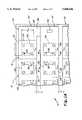
- FIG. 5is an isometric view of a passive RF transponder depicting a possible implementation of the peripheral high value capacitor of the present invention as a power supply filter capacitor integrated on a common substrate with a ferroelectric memory array and other associated functional logic blocks.
- Peripheral capacitor 10comprises, in pertinent part, an array of individual capacitors laid out in either linear elements or contiguous segments therewith comprising an array of capacitors ultimately to be connected in parallel such that the total capacitance of the peripheral capacitor 10 is equal to the sum of the capacitance of the individual capacitors in the array.
- Peripheral capacitor 10includes, a capacitor 12 ("C 1N-1 ”) and a capacitor 14 ("C 1N ”) forming individual capacitive devices of linear element 20 comprising a number of capacitors C 1 through C 1N . Additionally shown is a capacitor 16 ("C 2N-1 ”) and capacitor 18 ("C 2N ”) forming a portion of the capacitive devices of contiguous segment 22. Contiguous segment 22 comprises capacitors C 2 -C 2N . The total capacitance of linear element 20 and contiguous segment 22 is then:
- Peripheral capacitor 10may comprise any number of individual linear elements 20 having their bottom electrodes 26 interconnected by an additional conductive element, with or without associated contiguous segments 22, in the fabrication of a high value peripheral capacitor 10 in accordance with the present invention. As shown, linear element 20 is electrically connected to contiguous segment 22 at the bottom electrode 26 thereof by means of connecting structure 24.
- Linear element 20is separated in a parallel and spaced-apart manner from contiguous segment 22 by a distance C s between each of the individual capacitive devices thereof, which distance is dependent upon the capabilities of the process utilized.
- Other linear elements 20 or contiguous segments 22are also separated by the same distance C s as shown.
- each of the remaining capacitive devices of the peripheral capacitor 10may be determined inasmuch as each capacitor 12-18 of the peripheral capacitor 10 is like constructed.
- the area of capacitors 12-18are defined by a linear length dimension of TE L and and a linear width dimension TE W .
- Bottom electrode 26,may be in a preferred embodiment, comprised of platinum ("Pt"), platinum/titanium ("Pt/Ti”) or other noble metal or alloys thereof.
- the connecting structure 24 between linear element 20 and contiguous segment 22comprises a conductive element formed at the same time as bottom electrode 26 as will be more fully described hereinafter.
- a co-extensive ferroelectric layer 28which, in a preferred embodiment, may comprise a lead-zirconate-titanate (“PZT”) ferroelectric material proprietary to Ramtron International Corporation of Colorado Springs, Colo.
- the ferroelectric layer 28forms a dielectric material overlying bottom electrode 26 of capacitors 12-18. It should be noted that the ferroelectric layer 28 should not overlay the connecting structure 24 so as to allow connection to be made to the bottom electrode 26.
- a top electrode 30,which may have an area of TE L by TE W , is formed on top of the ferroelectric layer 28. Top electrode 30 in a preferred embodiment may be the same material as that utilized to construct bottom electrode 26.
- top electrode contacts 32are formed to provide electrical connection to the top electrode 30 of the individual capacitive devices of the peripheral capacitor 10.
- the top electrode contacts 32comprise four individual, substantially square cross-sectioned contacts adjacent the corners of the top electrode 30.
- any number of top electrode contacts 32may be utilized and any desired configuration of one or more of the top electrode contacts 32 may likewise be employed.
- a bottom electrode contact 34is provided to provide electrical contact to the bottom electrode 26 of the linear element 20 and contiguous segment 22 in conjunction with the connecting structure 24 therebetween.
- Bottom electrode contact 34may be established utilizing the same processing steps to provide the top electrode contacts 32 as will be more fully described hereinafter.
- a single bottom electrode contact 34may be employed, as shown, to provide contact to the bottom electrode 26 of a linear element 20 and associated contiguous segment 22 of the peripheral capacitor 10.
- a single bottom electrode contact 34may be employed to provide electrical contact to the bottom electrode 26 of an individual linear element 20 comprising a number of capacitive devices.
- metalization layer 36which may be, in a preferred embodiment, an aluminum (“Al”) conductive layer provides one terminal for the total parallel capacitance of peripheral capacitor 10.
- metalization layer 38which is formed to provide electrical contact to the bottom electrode contact 34 as well as that of other bottom electrode contacts 34 of additional linear elements 20 and/or contiguous segments 22 comprising the peripheral capacitor 10. Electrical contact made between metalization layer 36 and metalization layer 38 would then comprise the parallel capacitance, ("C total ”) of all individual capacitive devices comprising the peripheral capacitor 10.
- Metalization layer 38may also be formed utilizing the same processing step as is utilized to provide metalization layer 36.
- FIG. 2Aa larger portion of the peripheral capacitor 10 is shown including capacitors 12-18 of the linear element 20 and contiguous segment 22 previously described.
- additional linear elements 20comprising capacitors 40 ("C 3 -C 3N "), capacitors 42 ("C 4 -C 4N “), and capacitors 44 ("C 5 -C 5N ”) are shown.
- FIG. 2Ba larger portion of the peripheral capacitor 10 corresponding to that shown in FIG. 2A is illustrated to further depict the overlying metalization layer 36 connecting the top electrode contacts 32 as well as the metalization layer 38 providing electrical contact to a number of bottom electrode contacts 34.
- a high-value capacitancemay be integrated on an integrated circuit substrate on the order of 1-10 nF or more consistent with the available on-chip real estate and peripheral capacitance requirements.
- the peripheral capacitor 10 of the present inventionmay be efficaciously produced utilizing the same processing steps as are used to construct the individual memory cell capacitors of the ferroelectric memory array.
- ferroelectric memory array cell capacitorsmay be oppositely polarized to store digital information representative of a logic level "one” or “zero” in accordance with the properties of a ferroelectric dielectric
- the individual capacitive devices of peripheral capacitor 10are polarized in but a single direction, that is, operated lineraly as a non-ferroelectric capacitor.
- FIGS. 3A-3Ha process sequence for the construction of the peripheral capacitor 10 of the present invention is shown. More particularly and as a representative example only, the process flow will ultimately establish capacitors 16 and 18 in conjunction with bottom electrode contact 34 of the connecting structure 24 illustrated in FIGS. 1A and 1B.
- a substrate 50is shown upon which the peripheral capacitor 10 and a ferroelectric memory device may be integrated.
- Substrate 50may be composed of any basic semiconducting material such as silicon and silicon dioxide, germanium, gallium arsenide and the like.
- Substrate 50may further be subjected to thermal oxidation or chemical vapor deposition ("CVD").
- the substrate 50may, of course, already be partially processed with other passive and/or active components or portions thereof. As shown, substrate 50 presents a substrate surface 52 for subsequent processing.
- a bottom electrode layer 54is shown as being applied to the substrate surface 52, and presenting a surface 56 oppositely disposed therefrom.
- the bottom electrode layer 54can be established, for example, by deposition or other known processing techniques.
- a dielectric layer 58is formed overlying the surface 56 of bottom electrode layer 54 and presents a dielectric surface 60 thereof.
- the dielectric layer 58which, in a preferred embodiment, comprises a lead-zirconate-titanate thin film structure proprietary to Ramtron International Corporation having a chemical composition of Pb(Ti x Zr 1-x )O 3 , wherein x is in the range of 0.2 to 1.0.
- the dielectric layer 58can be established by a number of known methods.
- the thickness of dielectric layer 58, when utilizing PZT,will be on the order of approximately 2,500-3,000 angstroms.
- a top electrode layer 62is formed on the dielectric surface 60 of dielectric layer 58 and patterned in subsequent processing steps to form a number of top electrodes as shown.
- the top electrode layer 62may be established, for example, by deposition using the same method and material as used to form the bottom electrode layer 54.
- the top electrode layer 62is then defined to produce the top electrodes of the peripheral capacitor 10. This definition process may be carried out by conventional semiconductor fabrication techniques such as photolithography and plasma etching, other anisotropic etch processes, wet etching or ion milling.
- the top electrode layer 62leaves remaining surfaces 64 in the area of the capacitive devices forming the peripheral capacitor 10.
- an insulating layer 66is overlaid on the surfaces 64 of the top electrode layer 62 as well as the dielectric surface 60 of the dielectric layer 58.
- Insulating layer 66which in a preferred embodiment may comprise silicon dioxide, can be established, by deposition processes such as CVD.
- Insulating layer 66which may also be made of other insulating materials, presents an upper surface 68.
- top electrode contact apertures 70are formed through the insulating layer 66 to the surfaces 64 of the top electrode layer 62 in the areas in which the capacitive devices of the peripheral capacitor 10 will be formed. Additionally, a bottom electrode contact aperture 72 is formed through the insulating layer 66 and dielectric layer 58 to provide access to the surface 56 of the bottom electrode layer 54. The bottom electrode contact aperture 72 is formed in the region of the connecting structure 24 illustrated in FIG. 1A.
- the top electrode contact aperture 70 and bottom electrode contact aperture 72may be defined by conventional photo patterning and etching techniques.
- a metalization layer 74is formed over the upper surfaces 68 of the insulating layer 66 in the region of the top electrode layer 62 such that electrical contact is made with the top electrode layer 62 through the top electrode contact apertures 70.
- Metalization layer 74which in a preferred embodiment may comprise aluminum, presents an upper surface 78 thereof.
- a metalization layer 76is formed in the region of the bottom electrode contact aperture 72 to provide electrical contact to the bottom electrode layer 54 through the insulating layer 66 and dielectric layer 58.
- Metalization layer 76may be conveniently formed at the same time as metalization layer 74 to provide first and second terminal contacts to the various capacitive devices of the peripheral capacitor 10 through appropriate, known patterning techniques. It should be noted that other conducting structures may be utilized in lieu of an aluminum metalization layer such as a metal silicide, a doped polycrystalline silicon or other conductors.
- Metalization layer 76presents an upper surface 80 thereof.
- a passivation layer 82has been applied overlying the metalization layers 74 and 76.
- the passivation layer 82can be utilized to cover the entire surface of the integrated circuit comprising the peripheral capacitor 10 and any additionally integrated ferroelectric memory array by utilizing a non-semiconductor dielectric such as CVD glass or other insulating material to aid in protecting any exposed regions of the integrated circuit.
- the passivation layerwould be removed from around any bonding or contacting pads of the resultant integrated circuit.
- capacitancevaries directly with the dielectric constant of the dielectric material and inversely with the dielectric thickness. This can be represented to a first approximation by the following equation where: C is the resultant capacitance per unit area, ⁇ 0 is the dielectric constant of free space; ⁇ d is the dielectric constant of the dielectric material; and d th is the thickness of the dielectric.
- the dielectric constant ⁇ dis approximately 3.9 with a typical thickness of about 250 ⁇ . Therefore:
- the typical SiO 2 DRAM capacitorhas a cell capacitance of on the order of 50 fF (0.05 pF), such a capacitor would have to be enlarged 20,000 times to produce an effective 1 nF capacitor utilizing the same processing steps to integrate it on the same substrate.
- the same 1 nF capacitorcould be made utilizing the same processing steps as are currently used to produce a PZT memory cell capacitor and be on the order of twenty five to thirty times smaller.
- FIGS. 4A and 4Ba partial top plan view and corresponding cross-sectional view of a pair of memory cells 100 forming a portion of a ferroelectric memory array with which the peripheral capacitor 10 of the present invention may be integrated is shown.
- the peripheral capacitor 10may be integrated utilizing the same processing step as are utilized to fabricate the memory capacitors 104 of the memory cells 100 of the integrated circuit ferroelectric array.
- Memory cells 100each comprise an access transistor 102 and associated memory capacitor 104.
- the access transistors 102are shown having a common connected drain terminal thereof coupled to metalization layer 106.
- Local interconnects 108couple the source terminals of the access transistors 102 to the associated memory capacitor 104.
- Memory cells 100 of the ferroelectric memory arrayare formed on a common substrate 110 which, in a preferred embodiment is coextensive with the previously described substrate 50 of peripheral capacitor 10 and monolithic therewith.
- a relatively thick field oxide region 112 comprising silicon dioxideunderlies each of the memory capacitors 104 as shown to preclude undesired parasitic effects.
- Source regions 114 and drain region 116are formed in an upper surface of the substrate 110 by an implantation or diffusion of, for example, an N+ material when utilizing a P type substrate 110.
- Gates 118 of the access transistors 102overlie the upper surface of substrate 110 adjacent the drain region 116 and corresponding source regions 114.
- Source region contacts 122 of the local interconnects 108 and drain contact 124 of the metalization layer 106contact the source regions 114 and drain region 116 respectively through apertures formed in the insulating layer 120.
- the bottom electrodes 126 of the memory capacitors 104are formed on top of the insulating layer 120 in a manner as previously described with respect to the peripheral capacitor 10.
- Bottom electrode 126may comprise platinum or a titanium/platinum alloy.
- dielectric layers 128Overlying bottom electrodes 126, and generally coextensive therewith, are formed dielectric layers 128 in a manner previously described with respect to the peripheral capacitor 10.
- Dielectric layers 128may comprise a PZT ferroelectric material.
- Top electrodes 130 of the memory capacitors 104are formed on top of the dielectric layers 128 as previously described. Top electrodes 130 may comprise, for example, platinum or other noble metal.
- Overlying the structure of memory capacitors 104 and the insulating layer overlying access transistors 102is formed an additional insulating layer 132 through which contact is made to the top electrodes 130 by means of the local interconnects 108.
- the peripheral capacitor 10 of the present inventionmay be integrated as a power supply voltage filter capacitor forming part of an integrated circuit which also includes a ferroelectric memory array 162 and other associated logic blocks utilized to construct a passive RF/ID transponder 150.
- the passive RF/ID transponder 150may be manufactured in a card-sized form factor having approximate physical dimensions of 3.375 inches (85.7 mm) by 2.125 inches (54.0 mm) by 0.030 inches (0.76 mm).
- Passive RF/ID transponder 150comprises, with respect to its primary functional elements, an antenna 152 (which may be a conductive coil external to the integrated circuit) for receiving an FSK modulated signal from an associated controller. Antenna 152 is also utilized to transmit a signal back to the controller indicative of information stored in the ferroelectric memory array 162 or otherwise "hardwired" in passive RF transponder 150. Signal output from the antenna 152 is applied to a timing circuit 154 for deriving a clock signal from the received FSK modulated RF signal and supplying the same to the FSK detector 170 as well as to a control logic circuit 158 and an address register 160.
- a source of power (Vout) for the passive RF transponder 150is derived by a power supply 156 utilizing the electromagnetic energy in the received FSK modulated RF signal.
- the peripheral capacitor 10which in the depicted application may have a nominal value of approximately 1.0-10 nF, couples Vout to the integrated circuit ground to serve a power supply filtering function.
- the control logic circuit 158controls the functionality of the passive RF transponder 150 and is utilized to selectively address specific word locations within the memory array 162 by means of the address register 160.
- Data representing commands or information data detected by means of the FSK detector 170is supplied to a register 164 to allow data to be either written to or read out from the memory array 162 at the address determined by the address register 160.
- Information to be transmitted back to the associated controlleris held in the register 164 and subsequently encoded by means of encoder circuit 166 for output to a modulator circuit 168.
- the output of the modulator circuit 168is supplied to the antenna 152 for transmission back to the associated controller.
- peripheral high value capacitormay be laid out with a single square structure in lieu of the elongate structure shown.
- peripheral high value capacitor of the present inventionhas been described with respect to a flat, or planar device, it may also be fabricated as a trench or stacked capacitor as well.
Landscapes
- Engineering & Computer Science (AREA)
- Radar, Positioning & Navigation (AREA)
- Remote Sensing (AREA)
- Power Engineering (AREA)
- Computer Hardware Design (AREA)
- Computer Networks & Wireless Communication (AREA)
- Physics & Mathematics (AREA)
- General Physics & Mathematics (AREA)
- Semiconductor Integrated Circuits (AREA)
- Semiconductor Memories (AREA)
Abstract
Description
C.sub.total =(ΣC.sub.1. . . C.sub.1N +ΣC.sub.2. . . C.sub.2N)
C=(ε.sub.0 *ε.sub.d)/d.sub.th
C=(ε.sub.0 *3.9)/250Å=0.02 ε.sub.0
C=(ε.sub.0 *1500)/(2500Å-3000Å)=0.50ε.sub.0 =>0.60ε.sub.0
Claims (11)
Priority Applications (2)
| Application Number | Priority Date | Filing Date | Title |
|---|---|---|---|
| US08/525,497US5608246A (en) | 1994-02-10 | 1995-09-08 | Integration of high value capacitor with ferroelectric memory |
| US08/544,470US5909624A (en) | 1994-02-10 | 1995-10-18 | Method of making integration of high value capacitor with ferroelectric memory |
Applications Claiming Priority (2)
| Application Number | Priority Date | Filing Date | Title |
|---|---|---|---|
| US19470694A | 1994-02-10 | 1994-02-10 | |
| US08/525,497US5608246A (en) | 1994-02-10 | 1995-09-08 | Integration of high value capacitor with ferroelectric memory |
Related Parent Applications (1)
| Application Number | Title | Priority Date | Filing Date |
|---|---|---|---|
| US19470694AContinuation | 1994-02-10 | 1994-02-10 |
Related Child Applications (1)
| Application Number | Title | Priority Date | Filing Date |
|---|---|---|---|
| US08/544,470ContinuationUS5909624A (en) | 1994-02-10 | 1995-10-18 | Method of making integration of high value capacitor with ferroelectric memory |
Publications (1)
| Publication Number | Publication Date |
|---|---|
| US5608246Atrue US5608246A (en) | 1997-03-04 |
Family
ID=22718615
Family Applications (2)
| Application Number | Title | Priority Date | Filing Date |
|---|---|---|---|
| US08/525,497Expired - LifetimeUS5608246A (en) | 1994-02-10 | 1995-09-08 | Integration of high value capacitor with ferroelectric memory |
| US08/544,470Expired - LifetimeUS5909624A (en) | 1994-02-10 | 1995-10-18 | Method of making integration of high value capacitor with ferroelectric memory |
Family Applications After (1)
| Application Number | Title | Priority Date | Filing Date |
|---|---|---|---|
| US08/544,470Expired - LifetimeUS5909624A (en) | 1994-02-10 | 1995-10-18 | Method of making integration of high value capacitor with ferroelectric memory |
Country Status (1)
| Country | Link |
|---|---|
| US (2) | US5608246A (en) |
Cited By (36)
| Publication number | Priority date | Publication date | Assignee | Title |
|---|---|---|---|---|
| US5817533A (en)* | 1996-07-29 | 1998-10-06 | Fujitsu Limited | High-yield methods of fabricating large substrate capacitors |
| US5917230A (en)* | 1997-04-09 | 1999-06-29 | United Memories, Inc. | Filter capacitor construction |
| US6081036A (en)* | 1996-04-19 | 2000-06-27 | Matsushita Electronics Corp. | Semiconductor device |
| US6141242A (en)* | 1997-04-14 | 2000-10-31 | International Business Machines Corporation | Low cost mixed memory integration with substantially coplanar gate surfaces |
| US6157979A (en)* | 1998-03-14 | 2000-12-05 | Advanced Technology Materials, Inc. | Programmable controlling device with non-volatile ferroelectric state-machines for restarting processor when power is restored with execution states retained in said non-volatile state-machines on power down |
| US6208500B1 (en)* | 1998-11-25 | 2001-03-27 | Microchip Technology Incorporated | High quality factor capacitor |
| US6259126B1 (en) | 1999-11-23 | 2001-07-10 | International Business Machines Corporation | Low cost mixed memory integration with FERAM |
| US6407669B1 (en)* | 2001-02-02 | 2002-06-18 | 3M Innovative Properties Company | RFID tag device and method of manufacturing |
| US6507476B1 (en)* | 1999-11-01 | 2003-01-14 | International Business Machines Corporation | Tuneable ferroelectric decoupling capacitor |
| US6532824B1 (en)* | 1999-07-09 | 2003-03-18 | Tokin Corporation | Capacitive strain sensor and method for using the same |
| US6574130B2 (en) | 2001-07-25 | 2003-06-03 | Nantero, Inc. | Hybrid circuit having nanotube electromechanical memory |
| WO2003046922A3 (en)* | 2001-11-16 | 2003-08-14 | Infineon Technologies Ag | Semiconductor arrangement comprising transistors based on organic semiconductors and non-volatile read-write memory cells |
| US20030199172A1 (en)* | 2001-07-25 | 2003-10-23 | Thomas Rueckes | Methods of nanotube films and articles |
| US6643165B2 (en) | 2001-07-25 | 2003-11-04 | Nantero, Inc. | Electromechanical memory having cell selection circuitry constructed with nanotube technology |
| WO2002075780A3 (en)* | 2001-03-21 | 2004-02-05 | Koninkl Philips Electronics Nv | Electronic device having dielectric material of high dielectric constant |
| US6693541B2 (en) | 2001-07-19 | 2004-02-17 | 3M Innovative Properties Co | RFID tag with bridge circuit assembly and methods of use |
| US6706402B2 (en) | 2001-07-25 | 2004-03-16 | Nantero, Inc. | Nanotube films and articles |
| US20040164289A1 (en)* | 2001-12-28 | 2004-08-26 | Nantero, Inc. | Electromechanical three-trace junction devices |
| US6784028B2 (en) | 2001-12-28 | 2004-08-31 | Nantero, Inc. | Methods of making electromechanical three-trace junction devices |
| US20040214366A1 (en)* | 2001-07-25 | 2004-10-28 | Nantero, Inc. | Electromechanical memory array using nanotube ribbons and method for making same |
| US6911682B2 (en) | 2001-12-28 | 2005-06-28 | Nantero, Inc. | Electromechanical three-trace junction devices |
| US20060082224A1 (en)* | 2004-10-13 | 2006-04-20 | Andrew Marshall | Segmented programmable capacitor array for improved density and reduced leakege |
| US20060252211A1 (en)* | 2002-07-30 | 2006-11-09 | Micron Technology, Inc. | ATOMIC LAYER DEPOSITED NANOLAMINATES OF HfO2/ZrO2 FILMS AS GATE DIELECTRICS |
| US20060267766A1 (en)* | 2005-05-30 | 2006-11-30 | Hynix Semiconductor Inc. | RFID device having nonvolatile ferroelectric capacitor |
| KR100673131B1 (en) | 2005-12-09 | 2007-01-22 | 주식회사 하이닉스반도체 | RFID Devices Including Nonvolatile Ferroelectric Memory |
| US20070018260A1 (en)* | 2001-07-25 | 2007-01-25 | Nantero, Inc. | Devices having vertically-disposed nanofabric articles and methods of making the same |
| US20070235826A1 (en)* | 2001-07-25 | 2007-10-11 | Nantero, Inc. | Devices having horizontally-disposed nanofabric articles and methods of making the same |
| US20070248758A1 (en)* | 2002-04-23 | 2007-10-25 | Ward Jonathan W | Methods of using pre-formed nanotubes to make carbon nanotube films, layers, fabrics, elements and articles |
| US20070273515A1 (en)* | 2004-10-08 | 2007-11-29 | Mackenzie J D | RF and/or RF identification tag/device having an integrated interposer, and methods for making and using the same |
| US20080299307A1 (en)* | 2001-07-25 | 2008-12-04 | Ward Jonathan W | Methods of making carbon nanotube films, layers, fabrics, ribbons, elements and articles |
| US20090111282A1 (en)* | 2003-01-13 | 2009-04-30 | Ward Jonathan W | Methods of using thin metal layers to make carbon nanotube films, layers, fabrics, ribbons, elements and articles |
| US20100127084A1 (en)* | 2008-11-25 | 2010-05-27 | Vikram Pavate | Printed Antennas, Methods of Printing an Antenna, and Devices Including the Printed Antenna |
| US8278225B2 (en)* | 2005-01-05 | 2012-10-02 | Micron Technology, Inc. | Hafnium tantalum oxide dielectrics |
| US20130027899A1 (en)* | 2011-07-29 | 2013-01-31 | Tessera, Inc. | Embedded passive integration |
| US8501563B2 (en) | 2005-07-20 | 2013-08-06 | Micron Technology, Inc. | Devices with nanocrystals and methods of formation |
| US8753952B2 (en) | 2011-09-08 | 2014-06-17 | Texas Instruments Incorporated | Integrated circuit with integrated decoupling capacitors |
Families Citing this family (16)
| Publication number | Priority date | Publication date | Assignee | Title |
|---|---|---|---|---|
| US5990513A (en)* | 1996-10-08 | 1999-11-23 | Ramtron International Corporation | Yield enhancement technique for integrated circuit processing to reduce effects of undesired dielectric moisture retention and subsequent hydrogen out-diffusion |
| US5998225A (en)* | 1997-12-17 | 1999-12-07 | Texas Instruments Incorporated | Method of fabricating an oxygen-stable layer/diffusion barrier/poly bottom electrode structure for high-K DRAMs using disposable-oxide processing |
| US6180446B1 (en)* | 1997-12-17 | 2001-01-30 | Texas Instruments Incorporated | Method of fabricating an oxygen-stable layer/diffusion barrier/poly bottom electrode structure for high-K DRAMS using disposable-oxide processing |
| US6171898B1 (en)* | 1997-12-17 | 2001-01-09 | Texas Instruments Incorporated | Method of fabricating an oxygen-stable layer/diffusion barrier/poly bottom electrode structure for high-K-DRAMS using a disposable-oxide processing |
| US6329915B1 (en)* | 1997-12-31 | 2001-12-11 | Intermec Ip Corp | RF Tag having high dielectric constant material |
| US6093585A (en)* | 1998-05-08 | 2000-07-25 | Lsi Logic Corporation | High voltage tolerant thin film transistor |
| US6417041B1 (en)* | 1999-03-26 | 2002-07-09 | Advanced Micro Devices, Inc. | Method for fabricating high permitivity dielectric stacks having low buffer oxide |
| US7259654B2 (en)* | 2000-02-28 | 2007-08-21 | Magellan Technology Pty Limited | Radio frequency identification transponder |
| US7248145B2 (en)* | 2000-02-28 | 2007-07-24 | Magellan Technology Oty Limited | Radio frequency identification transponder |
| US6566698B2 (en)* | 2000-05-26 | 2003-05-20 | Sony Corporation | Ferroelectric-type nonvolatile semiconductor memory and operation method thereof |
| CA2430242A1 (en)* | 2003-06-06 | 2004-12-06 | Kimihiko Ernst Sato | Large array of radio frequency id transponders deployed in an array by use of deploying rows of transponders that unwind from long spools of high strength fiber or tape with passive rfid transponders separated by fixed lengths |
| US8723654B2 (en) | 2010-07-09 | 2014-05-13 | Cypress Semiconductor Corporation | Interrupt generation and acknowledgment for RFID |
| US9846664B2 (en) | 2010-07-09 | 2017-12-19 | Cypress Semiconductor Corporation | RFID interface and interrupt |
| US9092582B2 (en) | 2010-07-09 | 2015-07-28 | Cypress Semiconductor Corporation | Low power, low pin count interface for an RFID transponder |
| TWI837879B (en) | 2016-12-29 | 2024-04-01 | 美商艾德亞半導體接合科技有限公司 | Bonded structures with integrated passive component |
| US11901281B2 (en) | 2019-03-11 | 2024-02-13 | Adeia Semiconductor Bonding Technologies Inc. | Bonded structures with integrated passive component |
Citations (28)
| Publication number | Priority date | Publication date | Assignee | Title |
|---|---|---|---|---|
| US3935083A (en)* | 1973-01-12 | 1976-01-27 | Hitachi, Ltd. | Method of forming insulating film on interconnection layer |
| US4707897A (en)* | 1976-02-17 | 1987-11-24 | Ramtron Corporation | Monolithic semiconductor integrated circuit ferroelectric memory device, and methods of fabricating and utilizing same |
| US4809225A (en)* | 1987-07-02 | 1989-02-28 | Ramtron Corporation | Memory cell with volatile and non-volatile portions having ferroelectric capacitors |
| US4853893A (en)* | 1987-07-02 | 1989-08-01 | Ramtron Corporation | Data storage device and method of using a ferroelectric capacitance divider |
| US4873664A (en)* | 1987-02-12 | 1989-10-10 | Ramtron Corporation | Self restoring ferroelectric memory |
| US4893272A (en)* | 1988-04-22 | 1990-01-09 | Ramtron Corporation | Ferroelectric retention method |
| JPH02260559A (en)* | 1989-03-31 | 1990-10-23 | Seiko Epson Corp | Semiconductor integrated circuit device |
| EP0415751A1 (en)* | 1989-08-30 | 1991-03-06 | Nec Corporation | Thin film capacitor and manufacturing method thereof |
| US5005102A (en)* | 1989-06-20 | 1991-04-02 | Ramtron Corporation | Multilayer electrodes for integrated circuit capacitors |
| JPH03108367A (en)* | 1989-09-21 | 1991-05-08 | Nec Corp | Integrated circuit |
| US5024964A (en)* | 1970-09-28 | 1991-06-18 | Ramtron Corporation | Method of making ferroelectric memory devices |
| US5031144A (en)* | 1990-02-28 | 1991-07-09 | Hughes Aircraft Company | Ferroelectric memory with non-destructive readout including grid electrode between top and bottom electrodes |
| JPH03218063A (en)* | 1990-01-23 | 1991-09-25 | Matsushita Electron Corp | Semiconductor integrated circuit device |
| EP0449484A1 (en)* | 1990-03-30 | 1991-10-02 | Hitachi, Ltd. | Semiconductor integrated circuit devices with capacitors |
| US5075817A (en)* | 1990-06-22 | 1991-12-24 | Ramtron Corporation | Trench capacitor for large scale integrated memory |
| US5109357A (en)* | 1988-04-22 | 1992-04-28 | Ramtron Corporation | DRAM memory cell and method of operation thereof for transferring increased amount of charge to a bit line |
| US5142437A (en)* | 1991-06-13 | 1992-08-25 | Ramtron Corporation | Conducting electrode layers for ferroelectric capacitors in integrated circuits and method |
| US5162890A (en)* | 1990-07-30 | 1992-11-10 | Ramtron Corporation | Stacked capacitor with sidewall insulation |
| US5166545A (en)* | 1991-07-10 | 1992-11-24 | Dallas Semiconductor Corporation | Power-on-reset circuit including integration capacitor |
| US5191510A (en)* | 1992-04-29 | 1993-03-02 | Ramtron International Corporation | Use of palladium as an adhesion layer and as an electrode in ferroelectric memory devices |
| JPH0589661A (en)* | 1991-02-15 | 1993-04-09 | Olympus Optical Co Ltd | Ferroelectric memory |
| US5206788A (en)* | 1991-12-12 | 1993-04-27 | Ramtron Corporation | Series ferroelectric capacitor structure for monolithic integrated circuits and method |
| JPH05135999A (en)* | 1991-11-08 | 1993-06-01 | Rohm Co Ltd | Dielectric film capacitor |
| US5216572A (en)* | 1992-03-19 | 1993-06-01 | Ramtron International Corporation | Structure and method for increasing the dielectric constant of integrated ferroelectric capacitors |
| JPH05267557A (en)* | 1992-03-17 | 1993-10-15 | Matsushita Electron Corp | Semiconductor device |
| US5266821A (en)* | 1988-05-31 | 1993-11-30 | Micron Technology, Inc. | Chip decoupling capacitor |
| US5338951A (en)* | 1991-11-06 | 1994-08-16 | Ramtron International Corporation | Structure of high dielectric constant metal/dielectric/semiconductor capacitor for use as the storage capacitor in memory devices |
| US5350705A (en)* | 1992-08-25 | 1994-09-27 | National Semiconductor Corporation | Ferroelectric memory cell arrangement having a split capacitor plate structure |
Family Cites Families (2)
| Publication number | Priority date | Publication date | Assignee | Title |
|---|---|---|---|---|
| US5046043A (en)* | 1987-10-08 | 1991-09-03 | National Semiconductor Corporation | Ferroelectric capacitor and memory cell including barrier and isolation layers |
| US5384729A (en)* | 1991-10-28 | 1995-01-24 | Rohm Co., Ltd. | Semiconductor storage device having ferroelectric film |
- 1995
- 1995-09-08USUS08/525,497patent/US5608246A/ennot_activeExpired - Lifetime
- 1995-10-18USUS08/544,470patent/US5909624A/ennot_activeExpired - Lifetime
Patent Citations (28)
| Publication number | Priority date | Publication date | Assignee | Title |
|---|---|---|---|---|
| US5024964A (en)* | 1970-09-28 | 1991-06-18 | Ramtron Corporation | Method of making ferroelectric memory devices |
| US3935083A (en)* | 1973-01-12 | 1976-01-27 | Hitachi, Ltd. | Method of forming insulating film on interconnection layer |
| US4707897A (en)* | 1976-02-17 | 1987-11-24 | Ramtron Corporation | Monolithic semiconductor integrated circuit ferroelectric memory device, and methods of fabricating and utilizing same |
| US4873664A (en)* | 1987-02-12 | 1989-10-10 | Ramtron Corporation | Self restoring ferroelectric memory |
| US4809225A (en)* | 1987-07-02 | 1989-02-28 | Ramtron Corporation | Memory cell with volatile and non-volatile portions having ferroelectric capacitors |
| US4853893A (en)* | 1987-07-02 | 1989-08-01 | Ramtron Corporation | Data storage device and method of using a ferroelectric capacitance divider |
| US4893272A (en)* | 1988-04-22 | 1990-01-09 | Ramtron Corporation | Ferroelectric retention method |
| US5109357A (en)* | 1988-04-22 | 1992-04-28 | Ramtron Corporation | DRAM memory cell and method of operation thereof for transferring increased amount of charge to a bit line |
| US5266821A (en)* | 1988-05-31 | 1993-11-30 | Micron Technology, Inc. | Chip decoupling capacitor |
| JPH02260559A (en)* | 1989-03-31 | 1990-10-23 | Seiko Epson Corp | Semiconductor integrated circuit device |
| US5005102A (en)* | 1989-06-20 | 1991-04-02 | Ramtron Corporation | Multilayer electrodes for integrated circuit capacitors |
| EP0415751A1 (en)* | 1989-08-30 | 1991-03-06 | Nec Corporation | Thin film capacitor and manufacturing method thereof |
| JPH03108367A (en)* | 1989-09-21 | 1991-05-08 | Nec Corp | Integrated circuit |
| JPH03218063A (en)* | 1990-01-23 | 1991-09-25 | Matsushita Electron Corp | Semiconductor integrated circuit device |
| US5031144A (en)* | 1990-02-28 | 1991-07-09 | Hughes Aircraft Company | Ferroelectric memory with non-destructive readout including grid electrode between top and bottom electrodes |
| EP0449484A1 (en)* | 1990-03-30 | 1991-10-02 | Hitachi, Ltd. | Semiconductor integrated circuit devices with capacitors |
| US5075817A (en)* | 1990-06-22 | 1991-12-24 | Ramtron Corporation | Trench capacitor for large scale integrated memory |
| US5162890A (en)* | 1990-07-30 | 1992-11-10 | Ramtron Corporation | Stacked capacitor with sidewall insulation |
| JPH0589661A (en)* | 1991-02-15 | 1993-04-09 | Olympus Optical Co Ltd | Ferroelectric memory |
| US5142437A (en)* | 1991-06-13 | 1992-08-25 | Ramtron Corporation | Conducting electrode layers for ferroelectric capacitors in integrated circuits and method |
| US5166545A (en)* | 1991-07-10 | 1992-11-24 | Dallas Semiconductor Corporation | Power-on-reset circuit including integration capacitor |
| US5338951A (en)* | 1991-11-06 | 1994-08-16 | Ramtron International Corporation | Structure of high dielectric constant metal/dielectric/semiconductor capacitor for use as the storage capacitor in memory devices |
| JPH05135999A (en)* | 1991-11-08 | 1993-06-01 | Rohm Co Ltd | Dielectric film capacitor |
| US5206788A (en)* | 1991-12-12 | 1993-04-27 | Ramtron Corporation | Series ferroelectric capacitor structure for monolithic integrated circuits and method |
| JPH05267557A (en)* | 1992-03-17 | 1993-10-15 | Matsushita Electron Corp | Semiconductor device |
| US5216572A (en)* | 1992-03-19 | 1993-06-01 | Ramtron International Corporation | Structure and method for increasing the dielectric constant of integrated ferroelectric capacitors |
| US5191510A (en)* | 1992-04-29 | 1993-03-02 | Ramtron International Corporation | Use of palladium as an adhesion layer and as an electrode in ferroelectric memory devices |
| US5350705A (en)* | 1992-08-25 | 1994-09-27 | National Semiconductor Corporation | Ferroelectric memory cell arrangement having a split capacitor plate structure |
Non-Patent Citations (8)
| Title |
|---|
| Liu et al, "Low-Temperature Fabrication of Amorphous BaTiO3 Thin-Film Bypass Capacitors," IEEE Electron Device Letters, vol. 14 No. 7, 1993, pp. 320-322. |
| Liu et al, Low Temperature Fabrication of Amorphous BaTiO 3 Thin Film Bypass Capacitors, IEEE Electron Device Letters , vol. 14 No. 7, 1993, pp. 320 322.* |
| Ramtron Corporation, R2 92490, Ramtron Brochure, RTx 0801 Ramtag , 256 Bit Passive Nonvolatile RF/ID Tag Engineering Prototype, 1990, pp. 1 6.* |
| Ramtron Corporation, R2 92490, Ramtron Brochure, RTx 0801 Ramtag™, 256-Bit Passive Nonvolatile RF/ID Tag Engineering Prototype, 1990, pp. 1-6. |
| Ramtron International Corporation, Ramtron Brochure, FM1208S FRAM Memory, 4,096 Bit Nonvolatile Ferroelectric RAM Product Specification, R3 Aug., 1993, pp. 1 8.* |
| Ramtron International Corporation, Ramtron Brochure, FM1208S FRAM® Memory, 4,096-Bit Nonvolatile Ferroelectric RAM Product Specification, R3 Aug., 1993, pp. 1-8. |
| Ramtron International corporation, Ramtron Brochure, Fram Technology, R7 020993, 1993.* |
| Ramtron International corporation, Ramtron Brochure, Fram® Technology, R7 020993, 1993. |
Cited By (82)
| Publication number | Priority date | Publication date | Assignee | Title |
|---|---|---|---|---|
| US6081036A (en)* | 1996-04-19 | 2000-06-27 | Matsushita Electronics Corp. | Semiconductor device |
| US5817533A (en)* | 1996-07-29 | 1998-10-06 | Fujitsu Limited | High-yield methods of fabricating large substrate capacitors |
| US5917230A (en)* | 1997-04-09 | 1999-06-29 | United Memories, Inc. | Filter capacitor construction |
| US6306744B1 (en) | 1997-04-09 | 2001-10-23 | United Microelectronics Corporation | Filter capacitor construction |
| US6141242A (en)* | 1997-04-14 | 2000-10-31 | International Business Machines Corporation | Low cost mixed memory integration with substantially coplanar gate surfaces |
| US6157979A (en)* | 1998-03-14 | 2000-12-05 | Advanced Technology Materials, Inc. | Programmable controlling device with non-volatile ferroelectric state-machines for restarting processor when power is restored with execution states retained in said non-volatile state-machines on power down |
| US6208500B1 (en)* | 1998-11-25 | 2001-03-27 | Microchip Technology Incorporated | High quality factor capacitor |
| US6532824B1 (en)* | 1999-07-09 | 2003-03-18 | Tokin Corporation | Capacitive strain sensor and method for using the same |
| US6507476B1 (en)* | 1999-11-01 | 2003-01-14 | International Business Machines Corporation | Tuneable ferroelectric decoupling capacitor |
| US20030112578A1 (en)* | 1999-11-01 | 2003-06-19 | International Business Machines Corporation | Tuneable ferroelectric decoupling capacitor |
| US6888714B2 (en) | 1999-11-01 | 2005-05-03 | International Business Machines Corporation | Tuneable ferroelectric decoupling capacitor |
| US6259126B1 (en) | 1999-11-23 | 2001-07-10 | International Business Machines Corporation | Low cost mixed memory integration with FERAM |
| US6407669B1 (en)* | 2001-02-02 | 2002-06-18 | 3M Innovative Properties Company | RFID tag device and method of manufacturing |
| WO2002075780A3 (en)* | 2001-03-21 | 2004-02-05 | Koninkl Philips Electronics Nv | Electronic device having dielectric material of high dielectric constant |
| US6936877B2 (en) | 2001-03-21 | 2005-08-30 | Koninklijke Philips Electronics N.V. | Integrated circuit including a capacitor with a high capacitance density |
| US6693541B2 (en) | 2001-07-19 | 2004-02-17 | 3M Innovative Properties Co | RFID tag with bridge circuit assembly and methods of use |
| US20050063210A1 (en)* | 2001-07-25 | 2005-03-24 | Nantero, Inc. | Hybrid circuit having nanotube electromechanical memory |
| US8101976B2 (en) | 2001-07-25 | 2012-01-24 | Nantero Inc. | Device selection circuitry constructed with nanotube ribbon technology |
| US20030199172A1 (en)* | 2001-07-25 | 2003-10-23 | Thomas Rueckes | Methods of nanotube films and articles |
| US6706402B2 (en) | 2001-07-25 | 2004-03-16 | Nantero, Inc. | Nanotube films and articles |
| US20040085805A1 (en)* | 2001-07-25 | 2004-05-06 | Nantero, Inc. | Device selection circuitry constructed with nanotube technology |
| US20040159833A1 (en)* | 2001-07-25 | 2004-08-19 | Nantero, Inc. | Nanotube films and articles |
| US7342818B2 (en) | 2001-07-25 | 2008-03-11 | Nantero, Inc. | Hybrid circuit having nanotube electromechanical memory |
| US7335528B2 (en) | 2001-07-25 | 2008-02-26 | Nantero, Inc. | Methods of nanotube films and articles |
| US7304357B2 (en) | 2001-07-25 | 2007-12-04 | Nantero, Inc. | Devices having horizontally-disposed nanofabric articles and methods of making the same |
| US20040214366A1 (en)* | 2001-07-25 | 2004-10-28 | Nantero, Inc. | Electromechanical memory array using nanotube ribbons and method for making same |
| US6836424B2 (en) | 2001-07-25 | 2004-12-28 | Nantero, Inc. | Hybrid circuit having nanotube electromechanical memory |
| US6835591B2 (en) | 2001-07-25 | 2004-12-28 | Nantero, Inc. | Methods of nanotube films and articles |
| US20080299307A1 (en)* | 2001-07-25 | 2008-12-04 | Ward Jonathan W | Methods of making carbon nanotube films, layers, fabrics, ribbons, elements and articles |
| US7298016B2 (en) | 2001-07-25 | 2007-11-20 | Nantero, Inc. | Electromechanical memory array using nanotube ribbons and method for making same |
| US20030165074A1 (en)* | 2001-07-25 | 2003-09-04 | Nantero, Inc. | Hybrid circuit having nanotube electromechanical memory |
| US20070235826A1 (en)* | 2001-07-25 | 2007-10-11 | Nantero, Inc. | Devices having horizontally-disposed nanofabric articles and methods of making the same |
| US6919592B2 (en) | 2001-07-25 | 2005-07-19 | Nantero, Inc. | Electromechanical memory array using nanotube ribbons and method for making same |
| US7274078B2 (en) | 2001-07-25 | 2007-09-25 | Nantero, Inc. | Devices having vertically-disposed nanofabric articles and methods of making the same |
| US20050191495A1 (en)* | 2001-07-25 | 2005-09-01 | Nantero, Inc. | Nanotube films and articles |
| US6942921B2 (en) | 2001-07-25 | 2005-09-13 | Nantero, Inc. | Nanotube films and articles |
| US7264990B2 (en) | 2001-07-25 | 2007-09-04 | Nantero, Inc. | Methods of nanotubes films and articles |
| US6643165B2 (en) | 2001-07-25 | 2003-11-04 | Nantero, Inc. | Electromechanical memory having cell selection circuitry constructed with nanotube technology |
| US7056758B2 (en) | 2001-07-25 | 2006-06-06 | Nantero, Inc. | Electromechanical memory array using nanotube ribbons and method for making same |
| US7120047B2 (en) | 2001-07-25 | 2006-10-10 | Segal Brent M | Device selection circuitry constructed with nanotube technology |
| US6574130B2 (en) | 2001-07-25 | 2003-06-03 | Nantero, Inc. | Hybrid circuit having nanotube electromechanical memory |
| US7566478B2 (en) | 2001-07-25 | 2009-07-28 | Nantero, Inc. | Methods of making carbon nanotube films, layers, fabrics, ribbons, elements and articles |
| US7745810B2 (en) | 2001-07-25 | 2010-06-29 | Nantero, Inc. | Nanotube films and articles |
| US20070018260A1 (en)* | 2001-07-25 | 2007-01-25 | Nantero, Inc. | Devices having vertically-disposed nanofabric articles and methods of making the same |
| US20070141746A1 (en)* | 2001-07-25 | 2007-06-21 | Nantero, Inc. | Methods of nanotube films and articles |
| WO2003046922A3 (en)* | 2001-11-16 | 2003-08-14 | Infineon Technologies Ag | Semiconductor arrangement comprising transistors based on organic semiconductors and non-volatile read-write memory cells |
| US7208823B2 (en) | 2001-11-16 | 2007-04-24 | Infineon Technologies Ag | Semiconductor arrangement comprising transistors based on organic semiconductors and non-volatile read-write memory cells |
| US20050077606A1 (en)* | 2001-11-16 | 2005-04-14 | Gunter Schmid | Semiconductor arrangement comprising transistors based on organic semiconductors and non-volatile read-writing memory cells |
| US20040191978A1 (en)* | 2001-12-28 | 2004-09-30 | Nantero, Inc. | Methods of making electromechanical three-trace junction devices |
| US6979590B2 (en) | 2001-12-28 | 2005-12-27 | Nantero, Inc. | Methods of making electromechanical three-trace junction devices |
| US6911682B2 (en) | 2001-12-28 | 2005-06-28 | Nantero, Inc. | Electromechanical three-trace junction devices |
| US7915066B2 (en) | 2001-12-28 | 2011-03-29 | Nantero, Inc. | Methods of making electromechanical three-trace junction devices |
| US7521736B2 (en) | 2001-12-28 | 2009-04-21 | Nantero, Inc. | Electromechanical three-trace junction devices |
| US7176505B2 (en) | 2001-12-28 | 2007-02-13 | Nantero, Inc. | Electromechanical three-trace junction devices |
| US6784028B2 (en) | 2001-12-28 | 2004-08-31 | Nantero, Inc. | Methods of making electromechanical three-trace junction devices |
| US20040164289A1 (en)* | 2001-12-28 | 2004-08-26 | Nantero, Inc. | Electromechanical three-trace junction devices |
| US20070248758A1 (en)* | 2002-04-23 | 2007-10-25 | Ward Jonathan W | Methods of using pre-formed nanotubes to make carbon nanotube films, layers, fabrics, elements and articles |
| US7335395B2 (en) | 2002-04-23 | 2008-02-26 | Nantero, Inc. | Methods of using pre-formed nanotubes to make carbon nanotube films, layers, fabrics, ribbons, elements and articles |
| US20060252211A1 (en)* | 2002-07-30 | 2006-11-09 | Micron Technology, Inc. | ATOMIC LAYER DEPOSITED NANOLAMINATES OF HfO2/ZrO2 FILMS AS GATE DIELECTRICS |
| US20090111282A1 (en)* | 2003-01-13 | 2009-04-30 | Ward Jonathan W | Methods of using thin metal layers to make carbon nanotube films, layers, fabrics, ribbons, elements and articles |
| US7560136B2 (en) | 2003-01-13 | 2009-07-14 | Nantero, Inc. | Methods of using thin metal layers to make carbon nanotube films, layers, fabrics, ribbons, elements and articles |
| US9953259B2 (en)* | 2004-10-08 | 2018-04-24 | Thin Film Electronics, Asa | RF and/or RF identification tag/device having an integrated interposer, and methods for making and using the same |
| US20070273515A1 (en)* | 2004-10-08 | 2007-11-29 | Mackenzie J D | RF and/or RF identification tag/device having an integrated interposer, and methods for making and using the same |
| US8884765B2 (en) | 2004-10-08 | 2014-11-11 | Thin Film Electronics Asa | RF and/or RF identification tag/device having an integrated interposer, and methods for making and using the same |
| US20060082224A1 (en)* | 2004-10-13 | 2006-04-20 | Andrew Marshall | Segmented programmable capacitor array for improved density and reduced leakege |
| US7570076B2 (en)* | 2004-10-13 | 2009-08-04 | Texas Instruments Incorporated | Segmented programmable capacitor array for improved density and reduced leakage |
| US8524618B2 (en) | 2005-01-05 | 2013-09-03 | Micron Technology, Inc. | Hafnium tantalum oxide dielectrics |
| US8278225B2 (en)* | 2005-01-05 | 2012-10-02 | Micron Technology, Inc. | Hafnium tantalum oxide dielectrics |
| US7710240B2 (en) | 2005-05-30 | 2010-05-04 | Hynix Semiconductor Inc. | RFID device having nonvolatile ferroelectric capacitor |
| US20060267766A1 (en)* | 2005-05-30 | 2006-11-30 | Hynix Semiconductor Inc. | RFID device having nonvolatile ferroelectric capacitor |
| KR100732277B1 (en) | 2005-05-30 | 2007-06-25 | 주식회사 하이닉스반도체 | Modulation / demodulation device in RDF including nonvolatile ferroelectric memory |
| US8501563B2 (en) | 2005-07-20 | 2013-08-06 | Micron Technology, Inc. | Devices with nanocrystals and methods of formation |
| US8921914B2 (en) | 2005-07-20 | 2014-12-30 | Micron Technology, Inc. | Devices with nanocrystals and methods of formation |
| US7800481B2 (en) | 2005-12-09 | 2010-09-21 | Hynix Semiconductor Inc. | RFID device having a nonvolatile ferroelectric memory |
| KR100673131B1 (en) | 2005-12-09 | 2007-01-22 | 주식회사 하이닉스반도체 | RFID Devices Including Nonvolatile Ferroelectric Memory |
| US20100127084A1 (en)* | 2008-11-25 | 2010-05-27 | Vikram Pavate | Printed Antennas, Methods of Printing an Antenna, and Devices Including the Printed Antenna |
| US9016585B2 (en) | 2008-11-25 | 2015-04-28 | Thin Film Electronics Asa | Printed antennas, methods of printing an antenna, and devices including the printed antenna |
| US9361573B2 (en) | 2008-11-25 | 2016-06-07 | Thin Film Electronics Asa | Printed antennas, methods of printing an antenna, and devices including the printed antenna |
| US8970003B2 (en)* | 2011-07-29 | 2015-03-03 | Tessera, Inc. | Embedded passive integration |
| US20130027899A1 (en)* | 2011-07-29 | 2013-01-31 | Tessera, Inc. | Embedded passive integration |
| US8753952B2 (en) | 2011-09-08 | 2014-06-17 | Texas Instruments Incorporated | Integrated circuit with integrated decoupling capacitors |
| US9070575B2 (en) | 2011-09-08 | 2015-06-30 | Texas Instruments Incorporated | Integrated circuit with integrated decoupling capacitors |
Also Published As
| Publication number | Publication date |
|---|---|
| US5909624A (en) | 1999-06-01 |
Similar Documents
| Publication | Publication Date | Title |
|---|---|---|
| US5608246A (en) | Integration of high value capacitor with ferroelectric memory | |
| US5436477A (en) | Semiconductor memory device with high dielectric capacitor structure | |
| US5047817A (en) | Stacked capacitor for semiconductor memory device | |
| JPH0221652A (en) | Semiconductor storage device | |
| JPH0412564A (en) | Semiconductor storage device and its manufacturing method | |
| US5506748A (en) | Capacitor for semiconductor integrated circuit | |
| US5285092A (en) | Semiconductor memory device having a stacked type capacitor and manufacturing method therefor | |
| US6541281B2 (en) | Ferroelectric circuit element that can be fabricated at low temperatures and method for making the same | |
| US5357460A (en) | Semiconductor memory device having two transistors and at least one ferroelectric film capacitor | |
| KR100360592B1 (en) | Semiconductor devic and method for fabricating it | |
| US20020053694A1 (en) | Method of forming a memory cell with self-aligned contacts | |
| US5606189A (en) | Dynamic RAM trench capacitor device with contact strap | |
| US6191441B1 (en) | Ferroelectric memory device and its drive method | |
| US6352890B1 (en) | Method of forming a memory cell with self-aligned contacts | |
| US5180683A (en) | Method of manufacturing stacked capacitor type semiconductor memory device | |
| US6822276B1 (en) | Memory structure with a ferroelectric capacitor | |
| US7015531B2 (en) | FeRAM having bottom electrode connected to storage node and method for forming the same | |
| US5132240A (en) | Method for manufacturing a semiconductor device | |
| US5219781A (en) | Method for manufacturing semiconductor memory device having a stacked type capacitor | |
| KR980012376A (en) | Manufacturing Method of Semiconductor Device and Semiconductor Device | |
| US20010045591A1 (en) | Semiconductor device and method of manufacturing the same | |
| JPH0590607A (en) | Semiconductor memory cell | |
| JPH04365375A (en) | Semiconductor memory device and its manufacture | |
| JPH02135775A (en) | Semiconductor storage device and its manufacturing method | |
| JPH03180062A (en) | Semiconductor storage device and its manufacturing method |
Legal Events
| Date | Code | Title | Description |
|---|---|---|---|
| STCF | Information on status: patent grant | Free format text:PATENTED CASE | |
| AS | Assignment | Owner name:RAMTRON INTERNATIONAL CORPORATION, COLORADO Free format text:FIRST AMENDMENT TO PATENT SEC. AGMNT;ASSIGNOR:NATONAL ELECTRICAL BENEFIT FUND;REEL/FRAME:009756/0085 Effective date:19990115 Owner name:RAMTRON INTERNATIONAL CORPORATION, COLORADO Free format text:FIRST AMENDMENT TO PATENT SEC. AGMNT.;ASSIGNOR:NATONAL ELECTRICAL BENEFIT FUND;REEL/FRAME:009756/0085 Effective date:19990115 | |
| FEPP | Fee payment procedure | Free format text:PAYOR NUMBER ASSIGNED (ORIGINAL EVENT CODE: ASPN); ENTITY STATUS OF PATENT OWNER: LARGE ENTITY | |
| FPAY | Fee payment | Year of fee payment:4 | |
| AS | Assignment | Owner name:INFINEON TECHNOLOGIES AG, GERMANY Free format text:SECURITY INTEREST;ASSIGNOR:RAMTRON INTERNATIONAL CORPORATION;REEL/FRAME:012653/0747 Effective date:20020328 | |
| AS | Assignment | Owner name:RAMTRON INTERNATIONAL CORPORATION, COLORADO Free format text:RELEASE OF SECURITY AGREEMENT;ASSIGNOR:NATIONAL ELECTRICAL BENEFIT FUND;REEL/FRAME:014624/0077 Effective date:20040326 | |
| FPAY | Fee payment | Year of fee payment:8 | |
| AS | Assignment | Owner name:RAMTRON INTERNATIONAL CORPORATION, COLORADO Free format text:RELEASE OF SECURITY INTEREST;ASSIGNOR:INFINEON TECHNOLOGIES AG;REEL/FRAME:016976/0575 Effective date:20050704 | |
| FPAY | Fee payment | Year of fee payment:12 | |
| AS | Assignment | Owner name:SILICON VALLEY BANK, CALIFORNIA Free format text:SECURITY AGREEMENT;ASSIGNOR:RAMTRON INTERNATIONAL CORPORATION;REEL/FRAME:027905/0963 Effective date:20120229 | |
| AS | Assignment | Owner name:CYPRESS SEMICONDUCTOR CORPORATION, CALIFORNIA Free format text:ASSIGNMENT OF ASSIGNORS INTEREST;ASSIGNOR:RAMTRON INTERNATIONAL CORPORATION;REEL/FRAME:029408/0437 Effective date:20121203 | |
| AS | Assignment | Owner name:RAMTRON INTERNATIONAL CORPORATION, COLORADO Free format text:RELEASE;ASSIGNOR:SILICON VALLEY BANK;REEL/FRAME:035198/0959 Effective date:20120229 | |
| AS | Assignment | Owner name:MORGAN STANLEY SENIOR FUNDING, INC., NEW YORK Free format text:SECURITY INTEREST;ASSIGNORS:CYPRESS SEMICONDUCTOR CORPORATION;SPANSION LLC;REEL/FRAME:035240/0429 Effective date:20150312 | |
| AS | Assignment | Owner name:MORGAN STANLEY SENIOR FUNDING, INC., NEW YORK Free format text:CORRECTIVE ASSIGNMENT TO CORRECT THE 8647899 PREVIOUSLY RECORDED ON REEL 035240 FRAME 0429. ASSIGNOR(S) HEREBY CONFIRMS THE SECURITY INTERST;ASSIGNORS:CYPRESS SEMICONDUCTOR CORPORATION;SPANSION LLC;REEL/FRAME:058002/0470 Effective date:20150312 |