US5606572A - Integration of laser with photodiode for feedback control - Google Patents
Integration of laser with photodiode for feedback controlDownload PDFInfo
- Publication number
- US5606572A US5606572AUS08/217,531US21753194AUS5606572AUS 5606572 AUS5606572 AUS 5606572AUS 21753194 AUS21753194 AUS 21753194AUS 5606572 AUS5606572 AUS 5606572A
- Authority
- US
- United States
- Prior art keywords
- photodiode
- mirror
- substrate
- vcsel
- light emitting
- Prior art date
- Legal status (The legal status is an assumption and is not a legal conclusion. Google has not performed a legal analysis and makes no representation as to the accuracy of the status listed.)
- Expired - Lifetime
Links
Images


Classifications
- B—PERFORMING OPERATIONS; TRANSPORTING
- B82—NANOTECHNOLOGY
- B82Y—SPECIFIC USES OR APPLICATIONS OF NANOSTRUCTURES; MEASUREMENT OR ANALYSIS OF NANOSTRUCTURES; MANUFACTURE OR TREATMENT OF NANOSTRUCTURES
- B82Y20/00—Nanooptics, e.g. quantum optics or photonic crystals
- H—ELECTRICITY
- H01—ELECTRIC ELEMENTS
- H01S—DEVICES USING THE PROCESS OF LIGHT AMPLIFICATION BY STIMULATED EMISSION OF RADIATION [LASER] TO AMPLIFY OR GENERATE LIGHT; DEVICES USING STIMULATED EMISSION OF ELECTROMAGNETIC RADIATION IN WAVE RANGES OTHER THAN OPTICAL
- H01S5/00—Semiconductor lasers
- H01S5/02—Structural details or components not essential to laser action
- H01S5/026—Monolithically integrated components, e.g. waveguides, monitoring photo-detectors, drivers
- H01S5/0262—Photo-diodes, e.g. transceiver devices, bidirectional devices
- H01S5/0264—Photo-diodes, e.g. transceiver devices, bidirectional devices for monitoring the laser-output
- H—ELECTRICITY
- H01—ELECTRIC ELEMENTS
- H01S—DEVICES USING THE PROCESS OF LIGHT AMPLIFICATION BY STIMULATED EMISSION OF RADIATION [LASER] TO AMPLIFY OR GENERATE LIGHT; DEVICES USING STIMULATED EMISSION OF ELECTROMAGNETIC RADIATION IN WAVE RANGES OTHER THAN OPTICAL
- H01S5/00—Semiconductor lasers
- H01S5/04—Processes or apparatus for excitation, e.g. pumping, e.g. by electron beams
- H01S5/042—Electrical excitation ; Circuits therefor
- H01S5/0421—Electrical excitation ; Circuits therefor characterised by the semiconducting contacting layers
- H01S5/0422—Electrical excitation ; Circuits therefor characterised by the semiconducting contacting layers with n- and p-contacts on the same side of the active layer
- H01S5/0424—Electrical excitation ; Circuits therefor characterised by the semiconducting contacting layers with n- and p-contacts on the same side of the active layer lateral current injection
- H—ELECTRICITY
- H01—ELECTRIC ELEMENTS
- H01S—DEVICES USING THE PROCESS OF LIGHT AMPLIFICATION BY STIMULATED EMISSION OF RADIATION [LASER] TO AMPLIFY OR GENERATE LIGHT; DEVICES USING STIMULATED EMISSION OF ELECTROMAGNETIC RADIATION IN WAVE RANGES OTHER THAN OPTICAL
- H01S5/00—Semiconductor lasers
- H01S5/04—Processes or apparatus for excitation, e.g. pumping, e.g. by electron beams
- H01S5/042—Electrical excitation ; Circuits therefor
- H01S5/0425—Electrodes, e.g. characterised by the structure
- H01S5/04256—Electrodes, e.g. characterised by the structure characterised by the configuration
- H—ELECTRICITY
- H01—ELECTRIC ELEMENTS
- H01S—DEVICES USING THE PROCESS OF LIGHT AMPLIFICATION BY STIMULATED EMISSION OF RADIATION [LASER] TO AMPLIFY OR GENERATE LIGHT; DEVICES USING STIMULATED EMISSION OF ELECTROMAGNETIC RADIATION IN WAVE RANGES OTHER THAN OPTICAL
- H01S5/00—Semiconductor lasers
- H01S5/10—Construction or shape of the optical resonator, e.g. extended or external cavity, coupled cavities, bent-guide, varying width, thickness or composition of the active region
- H01S5/18—Surface-emitting [SE] lasers, e.g. having both horizontal and vertical cavities
- H01S5/183—Surface-emitting [SE] lasers, e.g. having both horizontal and vertical cavities having only vertical cavities, e.g. vertical cavity surface-emitting lasers [VCSEL]
- H01S5/18386—Details of the emission surface for influencing the near- or far-field, e.g. a grating on the surface
- H01S5/18394—Apertures, e.g. defined by the shape of the upper electrode
- H—ELECTRICITY
- H01—ELECTRIC ELEMENTS
- H01S—DEVICES USING THE PROCESS OF LIGHT AMPLIFICATION BY STIMULATED EMISSION OF RADIATION [LASER] TO AMPLIFY OR GENERATE LIGHT; DEVICES USING STIMULATED EMISSION OF ELECTROMAGNETIC RADIATION IN WAVE RANGES OTHER THAN OPTICAL
- H01S5/00—Semiconductor lasers
- H01S5/04—Processes or apparatus for excitation, e.g. pumping, e.g. by electron beams
- H01S5/042—Electrical excitation ; Circuits therefor
- H01S5/0425—Electrodes, e.g. characterised by the structure
- H01S5/04252—Electrodes, e.g. characterised by the structure characterised by the material
- H—ELECTRICITY
- H01—ELECTRIC ELEMENTS
- H01S—DEVICES USING THE PROCESS OF LIGHT AMPLIFICATION BY STIMULATED EMISSION OF RADIATION [LASER] TO AMPLIFY OR GENERATE LIGHT; DEVICES USING STIMULATED EMISSION OF ELECTROMAGNETIC RADIATION IN WAVE RANGES OTHER THAN OPTICAL
- H01S5/00—Semiconductor lasers
- H01S5/06—Arrangements for controlling the laser output parameters, e.g. by operating on the active medium
- H01S5/068—Stabilisation of laser output parameters
- H01S5/0683—Stabilisation of laser output parameters by monitoring the optical output parameters
- H—ELECTRICITY
- H01—ELECTRIC ELEMENTS
- H01S—DEVICES USING THE PROCESS OF LIGHT AMPLIFICATION BY STIMULATED EMISSION OF RADIATION [LASER] TO AMPLIFY OR GENERATE LIGHT; DEVICES USING STIMULATED EMISSION OF ELECTROMAGNETIC RADIATION IN WAVE RANGES OTHER THAN OPTICAL
- H01S5/00—Semiconductor lasers
- H01S5/10—Construction or shape of the optical resonator, e.g. extended or external cavity, coupled cavities, bent-guide, varying width, thickness or composition of the active region
- H01S5/1078—Construction or shape of the optical resonator, e.g. extended or external cavity, coupled cavities, bent-guide, varying width, thickness or composition of the active region with means to control the spontaneous emission, e.g. reducing or reinjection
- H—ELECTRICITY
- H01—ELECTRIC ELEMENTS
- H01S—DEVICES USING THE PROCESS OF LIGHT AMPLIFICATION BY STIMULATED EMISSION OF RADIATION [LASER] TO AMPLIFY OR GENERATE LIGHT; DEVICES USING STIMULATED EMISSION OF ELECTROMAGNETIC RADIATION IN WAVE RANGES OTHER THAN OPTICAL
- H01S5/00—Semiconductor lasers
- H01S5/10—Construction or shape of the optical resonator, e.g. extended or external cavity, coupled cavities, bent-guide, varying width, thickness or composition of the active region
- H01S5/18—Surface-emitting [SE] lasers, e.g. having both horizontal and vertical cavities
- H01S5/183—Surface-emitting [SE] lasers, e.g. having both horizontal and vertical cavities having only vertical cavities, e.g. vertical cavity surface-emitting lasers [VCSEL]
- H01S5/18308—Surface-emitting [SE] lasers, e.g. having both horizontal and vertical cavities having only vertical cavities, e.g. vertical cavity surface-emitting lasers [VCSEL] having a special structure for lateral current or light confinement
- H—ELECTRICITY
- H01—ELECTRIC ELEMENTS
- H01S—DEVICES USING THE PROCESS OF LIGHT AMPLIFICATION BY STIMULATED EMISSION OF RADIATION [LASER] TO AMPLIFY OR GENERATE LIGHT; DEVICES USING STIMULATED EMISSION OF ELECTROMAGNETIC RADIATION IN WAVE RANGES OTHER THAN OPTICAL
- H01S5/00—Semiconductor lasers
- H01S5/10—Construction or shape of the optical resonator, e.g. extended or external cavity, coupled cavities, bent-guide, varying width, thickness or composition of the active region
- H01S5/18—Surface-emitting [SE] lasers, e.g. having both horizontal and vertical cavities
- H01S5/183—Surface-emitting [SE] lasers, e.g. having both horizontal and vertical cavities having only vertical cavities, e.g. vertical cavity surface-emitting lasers [VCSEL]
- H01S5/18341—Intra-cavity contacts
- H—ELECTRICITY
- H01—ELECTRIC ELEMENTS
- H01S—DEVICES USING THE PROCESS OF LIGHT AMPLIFICATION BY STIMULATED EMISSION OF RADIATION [LASER] TO AMPLIFY OR GENERATE LIGHT; DEVICES USING STIMULATED EMISSION OF ELECTROMAGNETIC RADIATION IN WAVE RANGES OTHER THAN OPTICAL
- H01S5/00—Semiconductor lasers
- H01S5/10—Construction or shape of the optical resonator, e.g. extended or external cavity, coupled cavities, bent-guide, varying width, thickness or composition of the active region
- H01S5/18—Surface-emitting [SE] lasers, e.g. having both horizontal and vertical cavities
- H01S5/183—Surface-emitting [SE] lasers, e.g. having both horizontal and vertical cavities having only vertical cavities, e.g. vertical cavity surface-emitting lasers [VCSEL]
- H01S5/18358—Surface-emitting [SE] lasers, e.g. having both horizontal and vertical cavities having only vertical cavities, e.g. vertical cavity surface-emitting lasers [VCSEL] containing spacer layers to adjust the phase of the light wave in the cavity
- H—ELECTRICITY
- H01—ELECTRIC ELEMENTS
- H01S—DEVICES USING THE PROCESS OF LIGHT AMPLIFICATION BY STIMULATED EMISSION OF RADIATION [LASER] TO AMPLIFY OR GENERATE LIGHT; DEVICES USING STIMULATED EMISSION OF ELECTROMAGNETIC RADIATION IN WAVE RANGES OTHER THAN OPTICAL
- H01S5/00—Semiconductor lasers
- H01S5/20—Structure or shape of the semiconductor body to guide the optical wave ; Confining structures perpendicular to the optical axis, e.g. index or gain guiding, stripe geometry, broad area lasers, gain tailoring, transverse or lateral reflectors, special cladding structures, MQW barrier reflection layers
- H01S5/2054—Methods of obtaining the confinement
- H01S5/2059—Methods of obtaining the confinement by means of particular conductivity zones, e.g. obtained by particle bombardment or diffusion
- H—ELECTRICITY
- H01—ELECTRIC ELEMENTS
- H01S—DEVICES USING THE PROCESS OF LIGHT AMPLIFICATION BY STIMULATED EMISSION OF RADIATION [LASER] TO AMPLIFY OR GENERATE LIGHT; DEVICES USING STIMULATED EMISSION OF ELECTROMAGNETIC RADIATION IN WAVE RANGES OTHER THAN OPTICAL
- H01S5/00—Semiconductor lasers
- H01S5/30—Structure or shape of the active region; Materials used for the active region
- H01S5/34—Structure or shape of the active region; Materials used for the active region comprising quantum well or superlattice structures, e.g. single quantum well [SQW] lasers, multiple quantum well [MQW] lasers or graded index separate confinement heterostructure [GRINSCH] lasers
- H01S5/343—Structure or shape of the active region; Materials used for the active region comprising quantum well or superlattice structures, e.g. single quantum well [SQW] lasers, multiple quantum well [MQW] lasers or graded index separate confinement heterostructure [GRINSCH] lasers in AIIIBV compounds, e.g. AlGaAs-laser, InP-based laser
- H01S5/34313—Structure or shape of the active region; Materials used for the active region comprising quantum well or superlattice structures, e.g. single quantum well [SQW] lasers, multiple quantum well [MQW] lasers or graded index separate confinement heterostructure [GRINSCH] lasers in AIIIBV compounds, e.g. AlGaAs-laser, InP-based laser with a well layer having only As as V-compound, e.g. AlGaAs, InGaAs
- H01S5/3432—Structure or shape of the active region; Materials used for the active region comprising quantum well or superlattice structures, e.g. single quantum well [SQW] lasers, multiple quantum well [MQW] lasers or graded index separate confinement heterostructure [GRINSCH] lasers in AIIIBV compounds, e.g. AlGaAs-laser, InP-based laser with a well layer having only As as V-compound, e.g. AlGaAs, InGaAs the whole junction comprising only (AI)GaAs
Definitions
- This applicationrelates to the integration of surface light emitting devices with photodetectors and, in particular, to monolithic integration of superluminescent light emitting diodes (SLEDs) or vertical cavity surface emitting lasers (VCSELs) with photodetectors for feedback control of the radiation intensity of the SLEDs or VCSELs.
- SLEDssuperluminescent light emitting diodes
- VCSELsvertical cavity surface emitting lasers
- Semiconductor lasersare widely used in applications such as optical communications and compact disk players, etc.
- the optical intensity of the lasersis usually monitored for any intensity variation due to changing of the environment (e.g. temperature), heat generated by the laser circuitry, long-term drift of the laser properties, or drift of the properties of the circuitry that drives the laser.
- the intensity of the laseris monitored by a separate photodetector installed in the vicinity of the laser. The photodetector receives a small portion of the total optical radiation emitted from the laser and generates a feedback signal that corresponds to the intensity of the emitted radiation. This feedback signal is then provided to a feedback circuit that sends a control signal to the circuit that provides current to the laser.
- any drift of the laser intensityis detected and compensated by adjusting the current applied to the laser.
- the photodetectoris also used to verify the output optical pulses against the input of the electrical pulses.
- VCSELsvertical cavity surface emitting lasers
- a VCSELhas an optical cavity perpendicular to the substrate and emits optical radiation in a direction perpendicular to the substrate. Because of this structure, a VCSEL is more readily integrated with a photodiode than a conventional edge emitting laser.
- Hasnain et al.disclose an integrated device comprising a VCSEL and a PIN photodiode.
- the VCSELis epitaxially formed on a semiconductor substrate and the PIN photodiode is epitaxially formed on the VCSEL.
- the VCSELWhen operating, the VCSEL emits optical radiation which traverses the PIN photodiode. Accordingly, the photodiode absorbs a small portion of the optical radiation and generates a photocurrent which corresponds to the intensity of the radiation.
- the PIN photodiodeundesirable reflects and absorbs a portion of the light emitted from the VCSEL, which compromises the optical efficiency of the VCSEL.
- SLEDssuperluminescent light emitting diodes
- SLEDsCertain semiconductor diodes known as superluminescent light emitting diodes (SLEDs) also emit radiation in a direction perpendicular to the plane of the p-n junction. These SLEDs have a construction that is similar to that of a VCSEL except that one of the mirrors either is absent or has reduced reflectance such that the threshold conditions for lasing cannot be achieved.
- an integrated optoelectronic devicecomprises a vertical cavity surface emitting laser (VCSEL) and a photodiode.
- the VCSELcomprises first and second mirrors forming therebetween an optical cavity perpendicular to a substrate where the VCSEL is formed, and an active region disposed between the mirrors.
- the photodiodeis formed within the second mirror.
- the photodiodecomprises a plurality of semiconductor layers which also form a portion of the second mirror. Therefore, the photodiode is integrated with the VCSEL without introducing any undesirable optical perturbation from the photodiode.
- the photodiodecomprises materials having an energy bandgap equal to or smaller than the energy bandgap corresponding to the optical radiation, so that the photodiode intercepts and absorbs at least a portion of the optical radiation and generates a corresponding electrical signal.
- the second mirroris an epitaxially formed semiconductor distributed Bragg reflector (DBR) comprising a plurality of alternating semiconductor layers having high and low indices of refraction, with each layer having a thickness of ⁇ /4n where ⁇ is the wavelength of the optical radiation emitted from the laser and n is the index of refraction of the layer.
- the photodiodeis a PIN photodiode that comprises an undoped region interposed between a p-type region and an n-type region. Accordingly, each of the regions that form the PIN photodiode includes at least one of the layers that forms the second mirror.
- an integrated optoelectronic devicecomprises a substrate, a surface light emitting device formed on the substrate, the device emitting optical radiation having a wavelength, ⁇ , and a photodiode non-epitaxially formed on the surface emitting device.
- the surface light emitting devicemay be a SLED or a VCSEL.
- the VCSELcomprises first and second mirrors which form therebetween a vertical optical cavity, and an active region disposed between the mirrors.
- the photodiodeis non-epitaxially formed over the second mirror of the VCSEL.
- the second mirror of the lasercan be a semiconductor DBR or a dielectric DBR.
- the photodiodeis a polysilicon PN photodiode comprising a p-type polysilicon layer formed over an n-type polysilicon layer.
- the photodiodereceives optical radiation emitted from the VCSEL and generates a signal which corresponds to the intensity of the radiation.
- the structure of the deviceis the same except that one of the mirrors either is absent or has reduced reflectance.
- an integrated optoelectronic devicecomprises a VCSEL formed on a first surface of a substrate and a photodiode non-epitaxially formed on a second surface of the substrate.
- the photodiodeis substantially vertically aligned to the VCSEL for receiving optical radiation emitted from the laser.
- an integrated optoelectronic devicecomprises a semiconductor substrate, a surface light emitting device having a light-generating region formed on the substrate, at least the light-generating region forming a mesa having a substantially vertical outer surface, and a photodiode formed over the vertical outer surface of the mesa.
- the surface light emitting deviceemits a first optical radiation substantially orthogonal to the substrate, and a second optical radiation substantially parallel to the substrate.
- the photodiodereceives the second optical radiation and generates a corresponding electrical signal.
- the surface light emitting devicemay be a SLED or a VCSEL.
- the surface light emitting deviceis a VCSEL, it is formed on a substrate and a photodiode non-epitaxially formed on the side of the laser.
- the VCSELincludes first and second mirrors that form a vertical optical cavity, and an active region disposed between the mirrors.
- a mesa that includes at least the second mirror and the active regionis formed.
- the mesahas a sidewall which has a vertical outer surface.
- the photodiodeis formed on at least a portion of the outer surface of the mesa.
- the photodiodereceives lateral optical radiation from the active region of the VCSEL and generates a corresponding feedback signal.
- the structure of the deviceis the same except that one of the mirrors either is absent or has reduce reflectance.
- an integrated optoelectronic devicecomprises a VCSEL epitaxially formed on a first surface of a substrate and an implanted photodiode formed within the substrate and at a second surface of the substrate.
- the implanted photodiodeis vertically aligned with the VCSEL and receives optical radiation emitted from the laser.
- the implanted photodiodeis a PN photodiode comprising an implanted p-type region formed in an n-type substrate.
- an integrated optoelectronic devicecomprises a lateral injection VCSEL and a lateral PIN photodiode.
- the lateral injection VCSELcomprises first and second mirrors and an active region disposed between the mirrors.
- the laserfurther contains a first implantation region having a first conductivity type and a second implantation having a second conductivity type. Both the first and second implanted regions are formed at the periphery of the active region for applying a current to the active region.
- the devicefurther includes a third implantation region having a first conductivity type formed at the periphery of the active region; and the first, second, and third implantation regions do not overlap each other. Accordingly, the third implantation region, active region, and second implantation region together form a PIN photodiode, whereby a voltage between the second and third implantation regions indicates the intensity of the optical radiation emitted from the laser.
- a fourth implantation region having a second conductivity typeis formed at the periphery of the active region. Accordingly, the first and second implantation regions are utilized to inject current into the active region, whereas the third and fourth implantation regions and the active regions form the PIN photodiode.
- an integrated optoelectronic devicecomprises a substrate having a first conductivity type, a first mirror having a first conductivity type formed on the substrate, a first undoped spacer formed on the first mirror, an active region formed on the first spacer, a second undoped spacer formed on the active region, and a second mirror having a second conductivity type formed on the second spacer.
- the devicefurther includes an implanted isolation region formed within at least the second mirror, the spacers and the active region.
- the implanted isolation regionextends vertically from the second mirror to the first mirror, thereby dividing the second mirror, active region, and spacers into two portions, a first portion which is a VCSEL, and a second portion which is a PIN photodiode.
- the PIN photodiodereceives a laterally emitted optical radiation from the active region of the laser and generates a corresponding signal.
- the isolation regionseparates the laser and the PIN photodiode so that a voltage applied to the photodiode does not affect the laser.
- FIG. 1adepicts a cross-sectional view of a VCSEL integrated with a PIN photodiode epitaxially formed in a mirror of the VCSEL;
- FIG. 1billustrates, in more detail, a portion of the PIN photodiode of FIG. 1a;
- FIG. 1cdepicts an alternative embodiment of the VCSEL of FIG. 1a.
- FIG. 2ashows an equivalent circuit diagram of the integrated optoelectronic device of FIG. 1a
- FIG. 2billustrates an exemplary circuit configuration utilizing the device shown in FIG. 1a;
- FIG. 2cis a circuit diagram of feedback control of the laser intensity using the device shown in FIG. 1a;
- FIG. 3aillustrates a cross-section of a VCSEL integrated with an epitaxially formed PN photodiode
- FIG. 3bis a more detailed illustration of a portion of the PN photodiode shown in FIG. 3a;
- FIG. 4depicts a cross-section of a VCSEL integrated with a non-epitaxially formed PN photodiode
- FIG. 5illustrates a cross-section of a VCSEL integrated with a non-epitaxially formed PN photodiode formed on a back surface of a substrate
- FIG. 6depicts a cross-section of a VCSEL integrated with a PN photodiode non-epitaxially formed on the side of a mesa of the VCSEL;
- FIGS. 7a and 7billustrate cross-sectional and top views of an alternative embodiment of the device shown in FIG. 6;
- FIG. 8illustratively shows a cross-section of a VCSEL integrally formed with an implanted PN photodiode
- FIGS. 9a-9cdepict a cross-sectional view, a top view, and an equivalent circuit diagram, respectively, of a lateral injection VCSEL integrated with a lateral PIN photodiode;
- FIG. 9ddepicts a top view of an alternative embodiment of the device shown in FIG. 9a;
- FIG. 9edepicts a top view of another alternative embodiment of the device shown in FIG. 9a;
- FIG. 9fis a schematic circuit diagram for operating the device shown in FIG. 9e;
- FIG. 9gshows an equivalent circuit diagram of another possible circuit configuration using the device shown in FIG. 9e;
- FIG. 10aillustrates a top view of a VCSEL integrated with a PIN photodiode formed alongside of the VCSEL;
- FIG. 10billustrates a cross-section of the VCSEL shown in FIG. 10a
- FIG. 10cdepicts a cross-sections of the VCSEL and the PIN photodiode shown in FIG. 10a;
- FIG. 10dis an equivalent circuit diagram of the device shown in FIG. 10a.
- an optoelectronic devicecomprising a vertical cavity surface emitting laser (VCSEL) or a superluminescent light emitting diode (SLED) and a photodiode which is integrally formed with the VCSEL or SLED.
- VCSELvertical cavity surface emitting laser
- SLEDsuperluminescent light emitting diode
- the photodiodeintercepts the radiation and generates a feedback signal that corresponds to the intensity of the radiation.
- an integrated optoelectronic devicecomprises a VCSEL formed on a substrate and a photodiode formed in a mirror of the laser.
- the mirroris a semiconductor DBR comprising epitaxially formed layers having alternating high and low indices of refraction.
- the photodiodeis at least a portion of the mirror and is an integral part of the VCSEL.
- the photodiodeis a PIN photodiode or a PN photodiode.
- the photodiodecomprises semiconductor materials having a smaller bandgap than the effective bandgap of an active region of the VCSEL for absorbing the emitted light.
- FIG. 1aillustrates a cross-sectional view of a preferred embodiment of the device. It comprises an n-type first mirror 15, a first spacer 20, an active region 25 comprising AlGaAs/GaAs quantum wells, a second spacer 30, and a second mirror 35 formed on one side of an n-type GaAs substrate 10.
- the active regioncomprises InGaAs/GaAs quantum wells.
- Second mirror 35has two portions, a mesa portion 34, and a contact portion 33.
- contact portion 33is doped to have a p-type conductivity to provide an ohmic contact with contact 32.
- Contact 5 for the substrateis formed on the other side of the substrate.
- lower mirror 15is an n-doped semiconductor DBR comprising 20-30 periods of AlAs/AlGaAs layers.
- Each of these AlAs and AlGaAs layershas a thickness of ⁇ /(4n) where ⁇ is referred hereinafter as the wavelength of the emitted optical radiation in free space and n is the index of refraction of the layer.
- Second mirror 35is also a semiconductor DBR comprising alternating semiconductor layers of high and low indices of refraction.
- the layers that form the second mirrorare doped so that they form the PIN photodiode.
- second mirrorcomprises three portions, a lower p-type portion 40, an undoped layer 45, and an upper n-type portion 50.
- Lower portion 40comprises p-doped alternating layers of AlAs and AlGaAs, each layer having a thickness of ⁇ /(4n).
- Layer 45is an undoped GaAs layer having a thickness of ⁇ /(4n).
- Portion 50comprises n-doped alternating layers of AlAs and AlGaAs, each layer having a thickness of ⁇ /(4n).
- portions 40, 45, and 50form a PIN diode.
- GaAs layer 45 in the PIN photodiodehas a smaller bandgap than the effective bandgap of the active region for absorbing a portion of radiation emitted from the laser.
- layer 45is an InGaAs layer having an effective bandgap no greater than that of the active region for absorbing the optical radiation.
- optical radiation 60is emitted through the second mirror and the PIN photodiode absorbs a small portion of the radiation.
- the undoped portion of the PIN photodiodeis a single layer having a thickness of ⁇ /(4n).
- this undoped portioncan consist of more than one layer, each layer having a thickness of ⁇ /(4n).
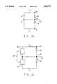
- FIG. 2adepicts an equivalent circuit diagram of the device shown in FIG. 1a.
- a VCSEL 70is serially connected with PIN photodiode 80.
- the VCSEL and photodiode anodesare common.
- FIG. 2bdepicts one of the possible configurations for utilizing the PIN photodiode to detect the radiation emitted from the VCSEL.
- contact 32is grounded.
- a positive voltage V Lis applied between contacts 32 and 5 to generate current I L which causes VCSEL 70 to radiate.
- PIN diode 80is reversed biased by applying a positive voltage V P between contacts 55 and 32.
- the light emitted from the VCSELgenerates a photocurrent I P which corresponds to the intensity of the emitted radiation.
- This photocurrentcan be utilized as a signal for feedback control of the VCSEL intensity or as an indicator of the VCSEL intensity.
- FIG. 2cillustrates a schematic diagram of a circuit for using the PIN photodiode for feedback control of the VCSEL intensity.
- photocurrent I Pis sent to a feedback circuit 85 which generates a signal 90 that corresponds to photocurrent I P .
- Signal 90is then sent to a laser controller 95.
- the laser controllerthen adjusts a laser driving current. I n in response to feedback signal 90 so as to maintain a constant magnitude of VCSEL intensity.
- a photovoltage generated from the photodiodecan also be utilized as the feedback signal that relates to the intensity of the radiation. Additionally, instead of grounding contact 32, contacts 5 and/or 55 may be grounded.
- the integrated optoelectronic device as shown in FIG. 1ais fabricated similarly to conventional VCSELs. All semiconductor layers, including layers for the first and second mirrors, the first and second spacers, and the active region, are epitaxially formed on a semiconductor substrate. Typically, Molecular Beam Epitaxy (MBE) or Metal Organic Chemical Vapor Deposition (MOCVD) technology is employed to epitaxially form these layers. Subsequently, the mesa portion of the second mirror is defined by etching the portion of the layers in region that surrounds the mesa.
- MBEMolecular Beam Epitaxy
- MOCVDMetal Organic Chemical Vapor Deposition
- contacts 5 for contacting n-doped substrate 10 and contact 32 for contacting p-doped mirror portion 33are also formed; and a ring-shaped contact 55 is formed on top of second mirror 35 to contact upper portion 50 of the PIN photodiode.
- contacts 5 and 55are contacts for n-doped semiconductor material, whereas contact 32 is a contact for p-type semiconductor material.
- portions 50 and 40 of the second mirrorcan be formed by depositing alternating layers of Al.sub.(1-x) Ga x As and Al.sub.(1-y) Ga y As where x and y are different values; or an annular p-type implanted region can be formed in the second spacer under contact 32 for reducing the contact resistance.
- the planar structure formed by deposition of the layers of the VCSELcan be left in place and an annular implantation region 36 can be formed in the planar structure.
- Implantation region 36should have a p-type conductivity type and extend vertically downward at least to the layer in p-type portion 40 of mirror 35.
- contact 32is formed on the surface of the implantation region and therefore is co-planar with contact 55.
- the implantation regionshould extend to second spacer 30 to reduce serial resistance of the laser.
- a PN photodiodeis formed in a mirror of a VCSEL.
- the cross-section of a preferred embodiment of this integrated optoelectronic deviceis illustrated in FIG. 3a. Since this device is very similar to the above described device wherein the detector is a PIN photodiode, like elements are designated with the same number in FIGS. 3a and 3b for convenience.
- second mirror 35comprises two portions, a p-type portion 40 and an n-type portion 50 that is formed on the p-type portion.
- at least one of the layers at the interface of portions 40 and 50should be a semiconductor layer having a bandgap equal or smaller than the effective bandgap of the active region.
- the two layers adjacent to the interface between p-type portion 40 and n-type portion 50are a p-type AlAs layer and an n-type GaAs layer. These two layers form a PN junction.
- portion 40comprises alternating p-type layers of AlAs and AlGaAs
- portion 50comprises an n-type GaAs layer formed on portion 40 and alternating n-type layers of AlAs and AlGaAs formed on the GaAs layer.
- FIG. 3aThe rest of the embodiment of FIG. 3a is the same as the embodiment shown in FIG. 1a and is not described here.
- an integrated optoelectronic devicecomprises a surface light emitting device such as a SLED or a VCSEL and a photodiode non-epitaxially formed on the surface light emitting device.
- This non-epitaxially formed photodiodeintercepts optical radiation emitted from the device and produces a feedback signal that corresponds to the intensity of the radiation.
- FIG. 4illustrates a preferred embodiment wherein the surface light emitting device is a VCSEL.
- the devicecomprises an n-type GaAs substrate 100, a first mirror 105 formed on the substrate, a first spacer 110, an active region 115 formed on the first spacer, a second spacer 125 formed on the active region, a first portion of a second mirror 130, a second portion of the second mirror 140, a polysilicon PN photodiode 158, and a protection layer 165 formed on the PN photodiode.
- This devicefurther includes an implanted annular current confinement region 132, an annular p-contact 135, contacts 145 and 160 for contacting the photodiode, and contact 95 for contacting the n-doped substrate.
- first mirror 105is a semiconductor DBR comprising 20-30 periods of AlAs/AlGaAs layers. Each of the AlAs or AlGaAs layers has a thickness of ⁇ /(4n). In addition, the first mirror is doped to have n-type conductivity.
- Active region 115comprises at least one GaAs quantum well.
- the two spacers 110, 125 surrounding the active regionare un-doped or low doped.
- the first portion of the second mirror 130is a p-type semiconductor DBR. Since the first portion is mainly used to provide ohmic contact with p-type contact 135, it typically contains only a few layers. Preferably, the first portion comprises approximately one to three periods of AlAs/AlGaAs layers, each AlAs or AlGaAs layer being ⁇ /(4n) thick. In addition, this first portion is doped to have p-type conductivity to assure ohmic contact with contact 135. Advantageously, since this first portion only contains a few layers, it is doped with p-dopant to a very high doping density (e.g., 10 18 -10 20 /cm 3 ) without significantly compromising the optical characteristics of the VCSEL.
- a very high doping densitye.g. 10 18 -10 20 /cm 3
- the second portion of the second mirroris a dielectric DBR comprising alternating layers of SiO 2 80 /and Si 3 N 4 , each of the layers having a thickness of ⁇ /(4n).
- the first and second portions of the second mirrorform the second mirror of the VCSEL. Accordingly, the first and second mirrors form therebetween a vertical optical cavity.
- Current confinement region 132is an annular region peripherally formed around the active region, the second spacer, the first portion of the second mirror, and a part of the first spacer. It is formed by implanting conductivity reducing ions such as Argon (Ar) or Helium (He). Consequently, this region exhibits high resistivity compared with its neighboring regions.
- conductivity reducing ionssuch as Argon (Ar) or Helium (He). Consequently, this region exhibits high resistivity compared with its neighboring regions.
- Contact 135is used to contact p-doped portion 130.
- itcomprises gold-beryllium (AuBe) or gold-zinc (AuZn) alloys.
- the substrate contact 95is formed to make ohmic contact to the n-type GaAs substrate and illustratively comprises gold-germanium alloy (AuGe).
- Polysilicon photodiode 158is formed on the second mirror. It comprises a p-type polysilicon layer 150, and a n-type polysilicon layer 155 formed on the p-type layer. Two peripheral contacts are formed to contact the two polysilicon layers. Illustratively, contact 160 is peripherally formed on the n-doped layer for contacting the n-type polysilicon layer 155, and contact 145 is peripherally formed under the p-doped layer for contacting the p-doped layer 150. Preferably, both contacts 145 and 160 are titanium silicide. Protection layer 165 is a SiO 2 layer formed on the photodiode.
- the fabrication of this devicebegins with sequentially growing the layers that form the first mirror, the first spacer, the active region, the second spacer, and the first portion of the second mirror.
- the current confinement regionis formed by performing an annular implantation of Argon or Helium.
- the implanted regionis damaged by the implantation so it has a substantially higher resistivity than the non-implanted regions. Therefore, current applied between contacts 135 and 95 is substantially confined to the active region.
- contact 135is formed by depositing a layer of gold-beryllium alloy and removing portions of the layer to define the shape of contact 135.
- the second portion of the second mirroris formed by depositing alternating layers of Si 3 N 4 and SiO 2 .
- the deposition of Si 3 N 4 and SiO 2 layeris well-known and is accomplished through techniques such as sputtering or chemical vapor deposition (CVD).
- a layer of titanium (Ti)is uniformly deposited onto the second mirror and etched to form contact 145.
- the polysilicon PN diodeis formed by first depositing p-doped polysilicon layer 150 and then n-doped polysilicon layer 155. Layers 150 and 155 form a PN junction.
- contact 160is formed by depositing another layer of titanium (Ti) and etching.
- protective layer 165is formed by depositing a layer of SiO 2 . Etching is subsequently performed to expose portions of contacts 160 and 145 so that they can be contacted by bonding wire 170 and 148.
- the structureis subsequently annealed so that contacts 145 and 160 titanium react with the polysilicon layers to form titanium-silicide.
- These titanium silicide layersform low-resistance ohmic contacts with layers 150 and 155, respectively.
- the annealing temperatureis between 400° to 500° C. and the annealing time is about 30 minutes.
- the thickness of Ti layers 145 and 160should be judiciously chosen so that they only form silicide within the layer they intend to contact.
- the formation of a silicide contact to a polysilicon layeris a well-developed technique in silicon semiconductor technology and therefore is not discussed in detail here.
- contact 95 on n-type GaAsis formed by depositing a layer of Ni and AuGe on substrate 100 and annealing.
- optical radiation 175is emitted from the laser. If the applied current exceeds the threshold current of the laser, coherent optical radiation 175 is generated.
- Optical radiation 175traverses polysilicon PN photodiode 158 which is reverse biased. Since the bandgap of polysilicon is smaller than the effective bandgap of the active region, a portion of the emitted radiation is absorbed by the polysilicon PN photodiode. Consequently, the PN photodiode produces a photocurrent that corresponds to the intensity of emitted radiation. Such current can be utilized as a feedback signal for controlling the intensity of radiation 175.
- contact polysilicon layer 150is to form contact 145 peripherally on layer 150, instead of forming it under layer 150.
- the process to fabricate such structureincludes forming polysilicon layers 150 and 155 onto the second mirror prior to forming contact 145. Subsequently, layer 155 is peripherally etched to expose a portion of layer 150. Contact 145 is then formed on this exposed area of layer 150.
- an integrated optoelectronic devicecomprises a VCSEL formed on a first surface of a substrate and a PN photodiode 188 non-epitaxially formed on a second surface of the substrate. Additionally, the PN photodiode is vertically aligned with the VCSEL. Thus, the PN photodiode intercepts optical radiation 203 emitted from the VCSEL and produces a current or voltage which corresponds to the intensity of radiation 230. Such current or voltage can be used as a feedback signal for controlling the intensity of radiation 230.
- the VCSELcomprises a first mirror 205 formed on a first surface 201 of substrate 200, a first spacer 210 formed on the first mirror, an active region 215 formed on the first spacer, a second spacer 220 formed on the active region, and a second mirror 225 formed on the second spacer.
- An isolation layer 195is formed on second surface 199 of the substrate.
- the PN photodiodecomprises a p-type polysilicon layer 190 non-epitaxially formed on the isolation layer, and a n-type polysilicon layer 185 non-epitaxially formed on the p-type polysilicon layer.
- a protective SiO 2 layer 180is formed on the n-type polysilicon layer.
- first mirror 205 and second mirror 225form therebetween a vertical optical cavity.
- First mirror 205is partially transmissive to allow radiation 203 to reach the photodiode.
- radiation 203has a wavelength corresponding to an energy bandgap that is not greater than that of the substrate. This can be achieved by forming the active region so that it has an effective energy bandgap that is not greater than that of the substrate.
- the substratecan be thinned to minimize absorption effects.
- radiation 203is only a portion of the total optical radiation emitted from the laser; for example, it is approximately 10% of the total radiation, whereas radiation 230 is about 90% of the total radiation.
- First mirror 205is a semiconductor DBR comprising a plurality of alternating layers of AlGaAs and AlAs, each of AlGaAs or AlAs having a thickness of ⁇ /(4n).
- the number of periods of AlGaAs/AlAs layers and the lasing wavelengthare judiciously chosen so that about 10% of total radiation transmits through the mirror 205.
- active region 215comprises one or more GaAs quantum wells and has an effective bandgap smaller than that of GaAs substrate 200.
- radiation 203goes through the substrate and reaches the photodiode without suffering significant attenuation in the substrate.
- GaAs substrate 200may be required to have a thickness of less than 100 ⁇ m. This reduces the absorption of radiation 203 in the substrate, so radiation 203 has the desired intensity when it reaches the photodiode.
- the active regionis laterally defined by an annular implanted current confinement region 217 which has substantially higher resistivity than the active region.
- the current confinement regionincludes peripheral portions of spacers 210 and 220.
- Second mirror 225comprises two portions, a first portion 221 and a second portion 222.
- First portion 221is a semiconductor DBR comprising one or more periods of AlGaAs/AlAs layers, each of the AlGaAs or AlAs layer having a thickness of ⁇ /4n. Additionally, the first portion of the second mirror is doped with p-type dopants to provide an ohmic contact with contact 223.
- Second portion of the second mirror 222is a dielectric DBR, or a semiconductor DBR.
- portion 222is a dielectric Bragg reflector comprising a plurality of alternating layers of Si 3 N 4 and SiO 2 , each of the Si 3 N 4 or SiO 2 layer having a thickness of ⁇ /4n.
- contacts 198, 189, and 182are formed to provide electrical contact to the substrate and the photodiode, respectively.
- epitaxial layers forming the first mirror, the spacers, the active region and the first portion of the second mirrorare first grown on the first Surface of the GaAs substrate.
- current confinement region 217is formed by an annular implantation of Ar ions.
- the second portion of the second mirroris constructed by depositing a series of alternating layers of SiO 2 and Si 3 N 4 onto the first portion of the second mirror. The deposition is conventionally accomplished by sputtering or other techniques.
- isolation layer 195is formed by depositing a layer of SiO 2 onto the back surface of the substrate.
- the polysilicon PN photodiodeis then constructed by depositing first a p-type polysilicon layer and then a n-type polysilicon layer.
- the polysilicon layersare formed by conventional Low Pressure Chemical Vapor Deposition (LPCVD) or evaporation. Subsequently, a SiO 2 protection layer is formed on the exposed polysilicon layer.
- LPCVDLow Pressure Chemical Vapor Deposition
- SiO 2 protection layeris formed on the exposed polysilicon layer.
- mesa etchingis performed to define the second portion of the second mirror and to expose an annular area of the first portion of the second mirror for formation of contact 223.
- etchingis also performed to expose peripheral areas of the substrate, the p-type polysilicon layer, and the n-type polysilicon layer.
- contacts for the laser and the polysilicon PN photodiodeare formed on those exposed areas.
- the polysilicon photodiodeis vertically aligned to the active region to receive maximum optical radiation emitted toward the photodiode.
- an integrated optoelectronic devicecomprises a surface light emitting device having a mesa, and a photodiode formed on the sidewall of the mesa.
- the surface light emitting devicemay be a SLED or a VCSEL.
- the photodiodeintercepts optical radiation laterally emitted from the surface light emitting device through the sidewall and provides a feedback signal that corresponds to the intensity of total radiation.
- the preferred embodiment of such integrated optoelectronic devicecomprises a VCSEL 310 having a mesa 312 and a polysilicon photodiode formed on a sidewall 313 of the mesa.
- the VCSELcomprises a substrate 300, a first mirror 305, a first spacer 315, an active region 320, a second spacer 325, and a second mirror 330.
- the VCSELfurther includes a peripheral contact 365 formed on the second mirror and a substrate contact 355.
- An annular current confinement region 335is formed to confine current applied to the VCSEL to the central portion of the VCSEL.
- optical radiationis emitted from the VCSEL.
- most of the radiationis emitted through the second mirror.
- Such radiationis designated as 370 in the Figure.
- a small portion of the total radiationis laterally emitted through the side wall of the mesa. This portion of radiation is designated as 385 in the Figure.
- photodiode 360intercepts radiation 385 and generates a feedback signal that relates to the intensity of radiation 370.
- the photodiodeis a polysilicon photodiode non-epitaxially formed on the sidewall.
- a portion of the photodiodeis formed on an annular horizontal surface 306 that surrounds the mesa.
- the photodiodecomprises a SiO 2 isolation layer 340, a p-type polysilicon layer 345, and an n-type polysilicon layer 350. These layers extend vertically on the sidewall to surface 306 where they then extend laterally on the horizontal surface. Contact 375 for contacting the n-type polysilicon layer and contact 380 for contacting the p-type polysilicon layer are formed on the horizontal portions of the layers.
- This preferred embodimentis fabricated by first constructing the VCSEL and then forming the polysilicon photodiode.
- the fabrication of the VCSELis well known and is similar to what have been described before, and therefore is not discussed in detail here.
- a SiO 2 isolation layeris formed by either sputtering or by CVD.
- p-type and n-type polysilicon layersare deposited and etched to form the structure depicted in FIG. 6.
- FIG. 6illustrates the PN photodiode formed on a portion of the sidewall.
- a ring-shaped PN photodiodeis formed to substantially cover the entire sidewall.
- FIGS. 7a and 7bshow the cross-sectional and top views of this embodiment.
- an integrated optoelectronic devicecomprises a VCSEL formed on a first surface of a substrate, and an implanted photodiode formed at a second surface and within the substrate.
- the implanted photodiodeintercepts optical radiation emitted from the laser and produces a feedback signal that corresponds to the intensity of the laser radiation.
- the preferred embodiment of this devicecomprises a VCSEL 408 formed on a first surface 401 of a substrate 400, and an implanted PN photodiode 402 formed at a second surface 403 of the substrate.
- the substrateis an n-type GaAs substrate doped to have a doping density of approximate10 18 /cm 3 .
- the VCSELcomprises a first mirror 405 formed on surface 401, a first spacer 410, an active region 415, a second spacer 425, and second mirror 430.
- the VCSELfurther includes a current confinement region 420, an upper contact 440, and a substrate contact 465.
- optical radiation 435radiates through the second mirror of the VCSEL.
- optical radiation 455is emitted from the VCSEL toward the implanted photodiode.
- first mirror 405is a semiconductor DBR comprising a plurality of alternating layers of AlGaAs and AlAs, each layer having a thickness of ⁇ /4n.
- mirror 405is partially transmissive so that about 10% of the emitted optical radiation is emitted toward the photodiode.
- the transmissivity of the first mirrorcan be changed by adjusting the number of layers of AlGaAs and AlAs that form the first mirror.
- the first mirroris doped to have n-type conductivity.
- Active region 415comprises at least one InGaAs quantum well. Since InGaAs quantum wells have an effective bandgap less than the bandgap of GaAs, radiation 455 does not suffer significant absorption in the substrate.
- Second mirror 430is a semiconductor DBR comprising a plurality of alternating AlGaAs and AlAs layers, each layer having a thickness of ⁇ /4n.
- the mirroris made to be more transmissive than the first mirror so that about 90% of total optical radiation is emitted through the second mirror.
- PN photodiode 402comprises a p-type implanted region 450 formed in the n-type GaAs substrate.
- the implanted p-type regionforms with the n-type GaAs substrate a pn junction which intercepts radiation 455.
- contact 460is formed to contact the p-type implanted region and contact 465 is formed to contact the substrate.
- a reverse bias voltageis applied to the pn junction through contacts 460 and 465, which produces a current that corresponds to the intensity of radiation 455.
- the fabrication of the VCSELwill be apparent to those skilled in the art, and therefore, is not discussed in detail here.
- the PN photodiodeis formed by ion implantation of p-type conductivity dopant into the n-type substrate.
- One way to fabricate this deviceis to first perform ion implantation on the back surface to form the PN photodiode, then to form epitaxial layers for the VCSEL on the front surface of the substrate. A thermal annealing process is usually employed after the implantation to activate the implanted dopants.
- epitaxial layers for the VCSELare first grown on the first surface of the substrate, followed by the ion implantation that forms the PN photodiode.
- the p-type implantation regionhas a diameter greater than the active region, and is vertically aligned with the active region.
- an optoelectronic devicecomprises a lateral injection VCSEL integrally formed with a lateral PIN photodiode.
- This deviceincludes three implanted regions formed at the periphery of an active region of the laser. The three implanted regions are first and third implanted regions having a first conductivity type, and a second implanted region having a second conductivity type.
- the first and third implanted regionsfacilitate applying current to the active region to generate optical radiation.
- the third implanted region, the active region, and the second implanted regiontogether form a lateral PIN photodiode wherein the voltage between the second and third implanted regions corresponds to the intensity of the optical radiation.
- a preferred embodiment of this integrated optoelectronic devicecomprises a GaAs semi-insulating substrate 500, a first mirror 505, a first spacer 510, an active region 515, a second spacer 530, and a second mirror 535.
- the devicefurther includes a first implanted region 520 having a p-type conductivity, a second implanted region 525 having a n-type conductivity, and a third implanted region 540 have a p-type conductivity.
- the devicealso includes contacts 545, 550, and 555 for contacting the first, second, and third implanted regions, respectively.
- FIG. 9bdepicts the top view of this device. Note that same elements are designated with the same numbers as in FIG. 9a.
- the first mirroris a semiconductor DBR comprising a plurality of alternating AlAs and AlGaAs layers, each of the AlAs and AlGaAs layers having a thickness of ⁇ /4n.
- the first mirroris formed on the semi-insulating GaAs substrate and is un-doped.
- the active regioncomprises at least one GaAs quantum well and is interposed between the two spacers.
- the second mirroris formed on the second spacer.
- the second mirroris a dielectric DBR comprising a plurality of alternating Si 3 N 4 and SiO 2 layers. Each of the Si 3 N 4 and SiO 2 layers that form the second mirror has a thickness equal to ⁇ /4n.
- the first and third implanted regionsare both doped with p-type dopants to have a high doping density of 10 18 /cm 3 .
- the second implantation regionis doped with n-type dopants such as Si.
- the density of n-type dopant in the second implanted regionis greater than10 18 cm 3 .
- the active region, the spacers and the mirrorsare all un-doped. Additionally, the three implanted regions do not overlap. Therefore, without any applied bias, the implanted regions are electrically isolated from each other.
- a voltageis applied between contacts 545 and 550 in this device, a current flows from the first to the second implanted region through the active region, thereby generating optical radiation 560. The intensity of such radiation is detected by measuring the voltage between contacts 550 and 555.
- FIG. 9cis a schematic circuit diagram for this device.
- a current source 565is used for driving a laser 518 which is the VCSEL described above.
- a voltmeter 570is used to measure the voltage across PIN photodiode 519 which corresponds to the voltage between contacts 550 and 555.
- the voltage of the lateral PIN photodiodeis utilized as a feedback signal representative of the VCSEL intensity.
- An alternative method of applying a reverse bias to the PIN photodiode and measuring the photocurrent of the PIN photodiodeis not applicable in this embodiment because the reverse bias undesirable affects the optical radiation of the VCSEL.
- This deviceis formed by first epitaxially growing layers that form the first mirror, the active region and the spacers on a semi-insulating GaAs substrate. Next, a p-type implantation is performed to form implanted regions 520 and 540. This is followed by an n-type implantation that forms implanted region 525. The implanted wafer is then thermally annealed through a rapid thermal anneal process to activate the implanted species. Subsequently, a series of alternating Si 3 N 4 and SiO 2 layers are deposited and etched to form the second mirror. Contacts 545 and 555 for contacting the p-type implanted regions and contact 550 for contacting the n-type implanted region are then formed.
- the active regionis circular and the implanted regions are formed around the periphery of the active region as shown in FIG. 9d.
- a fourth implanted region having a second type conductivityis incorporated in the embodiment of FIG. 9a.
- the top view of this embodimentis shown in FIG. 9e, wherein two implanted regions 550, 556 having n-type conductivity and two implanted regions 520, 555 having p-type conductivity are formed around the active region.
- FIG. 9fillustrates a circuit diagram for the device shown in FIG. 9e.
- two implanted regionsare utilized for introducing a driving current to the active region of the laser, whereas the other two implanted regions are used to measure the voltage from the PIN photodiode.
- applying current from regions 520 to 550generates optical radiation 560 from the laser, whereas a voltage that corresponds to the intensity of the radiation can be sensed between regions 555 and 556.
- FIG. 9gshows the schematic circuit diagram for another application of this device.
- the two implanted regions of the same conductivity typeare electrically connected to the ground potential.
- Two currents, I 1 and I 2 for driving the laserare applied to other two implanted regions, respectively.
- the devicecan be utilized as an electro-optic logic device.
- an integrated optoelectronic devicecomprises a VCSEL and a vertical photodiode epitaxially formed alongside the VCSEL.
- the photodiodeis a PIN photodiode and is isolated from the VCSEL by a surrounding implanted isolation region.
- FIG. 10adepicts a top view of the preferred embodiment of the device.
- a dash line enclosed portion 649is the top of the VCSEL
- another dash line enclosed portion 650is the top view of the PIN diode. Areas between the dash lines are areas of the implanted isolation region.
- a contact 640is formed for contacting the top of the VCSEL, and a contact 645 is formed as the anode contact of the PIN photodiode.
- FIG. 10bA cross-sectional view of the laser taken along line A-A' of FIG. 10a is illustrated in FIG. 10b.
- the VCSELcomprises an n-type GaAs substrate 600, a first n-type mirror 605, an un-doped first spacer 610, an un-doped active region 615 comprising at least one InGaAs quantum well, an un-doped second spacer 617, and a p-type second mirror 620.
- the VCSELfurther includes an implanted isolation region 625 that vertically extends from the second mirror to the first mirror.
- An annular current confinement region 630is formed around the active region.
- FIG. 10cdepicts a cross-sectional view taken from B-B' axis of FIG. 10a.
- PIN photodiode 650is formed alongside VCSEL to receive lateral optical radiation 643, and it contains the same epitaxial layers as the VCSEL.
- the PIN photodiodecomprises n-type layers 651, un-doped layers 652 and 654, and p-type layer 655.
- Layers 651, 652, 653, 654 and 655are portions of the same epitaxial layers that form the first mirror, the first spacer, the active region, the second spacer, and the second mirror of the VCSEL, respectively.
- the PIN photodiodeis vertically surrounded by isolation region 625.
- a contact 645is formed on the PIN photodiode to contact p-type layers 655.
- FIG. 10dillustrates the schematic circuit diagram of the use of this device to detect laser intensity.
- a current source 641is applied to laser contact 640 to drive the laser to emit radiation 642 along the vertical axis of the laser and radiation 643 in the lateral direction.
- PIN photodiode 650is reversed biased by a voltage V. The PIN photodiode receives the lateral optical radiation and generates a photocurrent I P which corresponds to the intensity of radiation 642.
- the first mirror 605is an n-type semiconductor DBR made from a plurality of alternating AlGaAs and AlAs layers, each having a thickness of ⁇ /4n.
- spacers 610 and 617are un-doped AlGaAs layers.
- the active region 615contains at least one InGaAs quantum well and has an effective bandgap energy less than GaAs.
- Second mirror 620is a p-type semiconductor DBR consisting of a plurality of alternating AlGaAs and AlAs layers, each having a thickness of ⁇ /4n.
- Isolation region 625is a region implanted with Ar and has high resistivity.
- the annular current confinement regionis also an Ar-implanted region peripherally formed around the active region.
- This integrated optoelectronic deviceis fabricated using conventional known and well-developed technologies.
- epitaxial layers forming the mirrors, spacers, and active regionare grown on an n-type GaAs substrate.
- the isolation regionis defined by photolithography and ion-implantation of Ar ions.
- another Ar-implantationis performed to form the annular current confinement region.
- a rapid thermal annealing processis employed to reduce the damage caused by the implantation.
- anode contacts for the laser and the PIN photodiode and a contact for the GaAs substrateare formed.
- the inventionmay also be practical using superluminescent light emitting diodes (SLEDs) in place of VCSELS.
- SLEDssuperluminescent light emitting diodes
- the SLEDsmay have the same structure as the VCSELs but be driven by currents below their threshold currents, or wherein the mirrors of the VCSELs are not efficient enough to produce a substantially stimulated optical radiation, i.e. laser radiation.
- all or part of one of the mirror structuresmay be eliminated so that lasing cannot occur.
Landscapes
- Physics & Mathematics (AREA)
- Optics & Photonics (AREA)
- Condensed Matter Physics & Semiconductors (AREA)
- General Physics & Mathematics (AREA)
- Electromagnetism (AREA)
- Chemical & Material Sciences (AREA)
- Engineering & Computer Science (AREA)
- Nanotechnology (AREA)
- Life Sciences & Earth Sciences (AREA)
- Biophysics (AREA)
- Crystallography & Structural Chemistry (AREA)
- Semiconductor Lasers (AREA)
Abstract
Description
Claims (15)
Priority Applications (4)
| Application Number | Priority Date | Filing Date | Title |
|---|---|---|---|
| US08/217,531US5606572A (en) | 1994-03-24 | 1994-03-24 | Integration of laser with photodiode for feedback control |
| AU21936/95AAU2193695A (en) | 1994-03-24 | 1995-03-24 | Integration of laser with photodiode for feedback control |
| PCT/US1995/003684WO1995026051A1 (en) | 1994-03-24 | 1995-03-24 | Integration of laser with photodiode for feedback control |
| US08/544,926US5577064A (en) | 1994-03-24 | 1995-10-18 | Integration of laser with photodiode for feedback control |
Applications Claiming Priority (1)
| Application Number | Priority Date | Filing Date | Title |
|---|---|---|---|
| US08/217,531US5606572A (en) | 1994-03-24 | 1994-03-24 | Integration of laser with photodiode for feedback control |
Related Child Applications (1)
| Application Number | Title | Priority Date | Filing Date |
|---|---|---|---|
| US08/544,926DivisionUS5577064A (en) | 1994-03-24 | 1995-10-18 | Integration of laser with photodiode for feedback control |
Publications (1)
| Publication Number | Publication Date |
|---|---|
| US5606572Atrue US5606572A (en) | 1997-02-25 |
Family
ID=22811455
Family Applications (2)
| Application Number | Title | Priority Date | Filing Date |
|---|---|---|---|
| US08/217,531Expired - LifetimeUS5606572A (en) | 1994-03-24 | 1994-03-24 | Integration of laser with photodiode for feedback control |
| US08/544,926Expired - LifetimeUS5577064A (en) | 1994-03-24 | 1995-10-18 | Integration of laser with photodiode for feedback control |
Family Applications After (1)
| Application Number | Title | Priority Date | Filing Date |
|---|---|---|---|
| US08/544,926Expired - LifetimeUS5577064A (en) | 1994-03-24 | 1995-10-18 | Integration of laser with photodiode for feedback control |
Country Status (3)
| Country | Link |
|---|---|
| US (2) | US5606572A (en) |
| AU (1) | AU2193695A (en) |
| WO (1) | WO1995026051A1 (en) |
Cited By (114)
| Publication number | Priority date | Publication date | Assignee | Title |
|---|---|---|---|---|
| US5724376A (en)* | 1995-11-30 | 1998-03-03 | Hewlett-Packard Company | Transparent substrate vertical cavity surface emitting lasers fabricated by semiconductor wafer bonding |
| US5729566A (en)* | 1996-06-07 | 1998-03-17 | Picolight Incorporated | Light emitting device having an electrical contact through a layer containing oxidized material |
| US5751757A (en)* | 1996-07-01 | 1998-05-12 | Motorola, Inc. | VCSEL with integrated MSM photodetector |
| US5757829A (en)* | 1996-04-29 | 1998-05-26 | Motorola, Inc. | Flip chip power monitoring system for vertical cavity surface emitting lasers |
| US5799030A (en)* | 1996-07-26 | 1998-08-25 | Honeywell Inc. | Semiconductor device with a laser and a photodetector in a common container |
| US5821566A (en)* | 1995-02-03 | 1998-10-13 | Samsung Electronics Co., Ltd. | Surface emitting semiconductor laser device and fabricating method of the same |
| US5887013A (en)* | 1996-10-29 | 1999-03-23 | Samsung Electronics Co. , Ltd. | Light emitting apparatus |
| US5900619A (en)* | 1995-07-26 | 1999-05-04 | Sony Corporation | Optical device comprising a photodetector for detecting light scattered outside a diffraction limit of an objective lens |
| WO1999034487A1 (en)* | 1997-12-31 | 1999-07-08 | Honeywell Inc. | Vertical cavity surface emitting laser having intensity |
| US5930276A (en)* | 1997-12-29 | 1999-07-27 | Motrola, Inc. | Method and device for providing temperature-stable optical feedback for optical packages |
| US5943357A (en)* | 1997-08-18 | 1999-08-24 | Motorola, Inc. | Long wavelength vertical cavity surface emitting laser with photodetector for automatic power control and method of fabrication |
| US5974071A (en)* | 1997-05-20 | 1999-10-26 | Motorola, Inc. | VCSEL with integrated photodetectors for automatic power control and signal detection in data storage |
| US6001664A (en)* | 1996-02-01 | 1999-12-14 | Cielo Communications, Inc. | Method for making closely-spaced VCSEL and photodetector on a substrate |
| US6002703A (en)* | 1998-01-28 | 1999-12-14 | University Of Utah Research Foundation | Gaussian profile promoting cavity for semiconductor laser |
| US6022760A (en)* | 1997-07-30 | 2000-02-08 | Motorola, Inc. | Integrated electro-optical package and method of fabrication |
| US6034431A (en)* | 1995-03-14 | 2000-03-07 | Lucent Technologies, Inc. | Electronic integrated circuit with optical inputs and outputs |
| US6037644A (en)* | 1997-09-12 | 2000-03-14 | The Whitaker Corporation | Semi-transparent monitor detector for surface emitting light emitting devices |
| US6091754A (en)* | 1998-04-27 | 2000-07-18 | Motorola, Inc. | VCSEL having integrated photodetector for automatic power control |
| US6160834A (en)* | 1998-11-14 | 2000-12-12 | Cielo Communications, Inc. | Vertical cavity surface emitting lasers with consistent slope efficiencies |
| US6222202B1 (en) | 1998-10-06 | 2001-04-24 | Agilent Technologies, Inc. | System and method for the monolithic integration of a light emitting device and a photodetector for low bias voltage operation |
| US6246708B1 (en) | 1997-08-27 | 2001-06-12 | Xerox Corporation | Semiconductor laser with associated electronic components integrally formed therewith |
| WO2001057977A1 (en)* | 2000-02-02 | 2001-08-09 | Infineon Technologies Ag | Vcsel with monolithically integrated photodetector |
| WO2002027877A1 (en)* | 2000-09-29 | 2002-04-04 | Osram Opto Semiconductors Gmbh | Semiconductor laser comprising a transparent contact surface |
| US6392256B1 (en)* | 1996-02-01 | 2002-05-21 | Cielo Communications, Inc. | Closely-spaced VCSEL and photodetector for applications requiring their independent operation |
| US20020085610A1 (en)* | 2000-12-29 | 2002-07-04 | Morgan Robert A. | Spatially modulated reflector for an optoelectronic device |
| US20020106160A1 (en)* | 2000-12-29 | 2002-08-08 | Honeywell International Inc. | Resonant reflector for increased wavelength and polarization control |
| WO2002084358A1 (en)* | 2001-04-18 | 2002-10-24 | Infineon Technologies Ag | Emission module for an optical signal transmission |
| US20030039284A1 (en)* | 2001-08-16 | 2003-02-27 | Jun Zheng | VCSEL with heat-spreading layer |
| US20030044737A1 (en)* | 2001-08-16 | 2003-03-06 | Eastman Kodak Company | Oriented polyester imaging element with nacreous pigment |
| US6535538B1 (en)* | 1999-11-08 | 2003-03-18 | Korea Advanced Institute Of Science And Technology | Surface emitting laser device with monolithically integrated monitor photodetector |
| EP0975072A3 (en)* | 1998-07-22 | 2003-03-19 | Canon Kabushiki Kaisha | Apparatus with an optical functional device having a special wiring electrode and method for fabricating the same |
| US20030076864A1 (en)* | 2001-10-23 | 2003-04-24 | Hironobu Sai | Surface light emitting type semiconductor laser having a vertical cavity |
| US20030096439A1 (en)* | 1999-09-20 | 2003-05-22 | Hsing-Chung Lee | Methods for forming index guided vertical cavity surface emitting lasers |
| US20030119222A1 (en)* | 2001-12-20 | 2003-06-26 | Pakulski Grzegorz J. | Hybrid confinement layers of buried heterostructure semiconductor laser |
| US20030133483A1 (en)* | 1997-12-12 | 2003-07-17 | Honeywell Inc. | VCSEL structure insensitive to mobile hydrogen |
| US20030138009A1 (en)* | 2002-01-09 | 2003-07-24 | Martin Weigert | Laser device |
| US6606199B2 (en) | 2001-10-10 | 2003-08-12 | Honeywell International Inc. | Graded thickness optical element and method of manufacture therefor |
| US20030151052A1 (en)* | 2001-05-02 | 2003-08-14 | Kenji Kawano | Semiconductor light receving element provided with acceleration spacer layers between plurality of light absorbing layers and method for fabricating the same |
| US6611003B1 (en)* | 1998-06-29 | 2003-08-26 | Kabushiki Kaisha Toshiba | Light emitting element and method of fabrication thereof |
| WO2002097934A3 (en)* | 2001-05-29 | 2003-10-23 | Nikolai Nikolaevich Ledentsov | Wavelenth-tunable vertical cavity surface emitting laser and method of making same |
| US20030209722A1 (en)* | 1999-12-22 | 2003-11-13 | Kabushiki Kaisha Toshiba | Light-emitting element and method of fabrication thereof |
| US6659659B1 (en) | 2001-04-11 | 2003-12-09 | Optical Communication Products, Inc. | High-speed optical sub-assembly utilizing ceramic substrate, direct coupling and laser welding |
| US20040028093A1 (en)* | 2002-05-08 | 2004-02-12 | Zarlink Semiconductor Ab | Photonic device with monitor |
| US20040042518A1 (en)* | 2002-09-03 | 2004-03-04 | Tatum James A. | Single mode VCSEL |
| US20040066820A1 (en)* | 2000-11-28 | 2004-04-08 | Johnson Ralph H. | Versatile method and system for single mode VCSELs |
| US20040069208A1 (en)* | 2000-07-14 | 2004-04-15 | Lommen Franciscus Alphons Marie | Process for crystallizing enantiomerically enriched 2-acetylthio-3-phenylpropionic acid |
| US20040081215A1 (en)* | 2002-10-28 | 2004-04-29 | Honeywell International Inc. | Distributed bragg reflector for optoelectronic device |
| US20040080011A1 (en)* | 2000-12-15 | 2004-04-29 | University Of Houston | One-chip micro-integrated optoelectronic sensor |
| US20040081467A1 (en)* | 2002-10-25 | 2004-04-29 | Taylor Geoff W. | Optoelectronic clock generator producing high frequency optoelectronic pulse trains with variable frequency and variable duty cycle and low jitter |
| US20040101009A1 (en)* | 2002-11-21 | 2004-05-27 | Honeywell International Inc. | Long wavelength VCSEL with tunnel junction, and implant |
| US6753214B1 (en)* | 2001-02-16 | 2004-06-22 | Optical Communication Products, Inc. | Photodetector with isolation implant region for reduced device capacitance and increased bandwidth |
| US6782027B2 (en) | 2000-12-29 | 2004-08-24 | Finisar Corporation | Resonant reflector for use with optoelectronic devices |
| US20040208216A1 (en)* | 2001-04-11 | 2004-10-21 | Naone Ryan Likeke | Long wavelength vertical cavity surface emitting laser |
| US20040222363A1 (en)* | 2003-05-07 | 2004-11-11 | Honeywell International Inc. | Connectorized optical component misalignment detection system |
| US20040245538A1 (en)* | 2003-06-06 | 2004-12-09 | Xiaolin Wang | Double sided optoelectronic integrated circuit |
| US20040247250A1 (en)* | 2003-06-03 | 2004-12-09 | Honeywell International Inc. | Integrated sleeve pluggable package |
| US20040247009A1 (en)* | 2001-07-05 | 2004-12-09 | Susumu Noda | Two-dimensional photonic crystal surface-emitting laser |
| US20040264855A1 (en)* | 2003-06-30 | 2004-12-30 | Bo Su Chen | Optical system with reduced back reflection |
| US20040264536A1 (en)* | 2003-06-27 | 2004-12-30 | Honeywell International Inc. | Dielectric VCSEL gain guide |
| US20040264530A1 (en)* | 2003-06-27 | 2004-12-30 | Honeywell International Inc. | VCSEL having thermal management |
| US20050013542A1 (en)* | 2003-07-16 | 2005-01-20 | Honeywell International Inc. | Coupler having reduction of reflections to light source |
| US20050013553A1 (en)* | 2003-07-16 | 2005-01-20 | Honeywell International Inc. | Optical coupling system |
| US20050014390A1 (en)* | 2003-07-18 | 2005-01-20 | Honeywell International Inc. | Edge bead control method and apparatus |
| US20050013539A1 (en)* | 2003-07-17 | 2005-01-20 | Honeywell International Inc. | Optical coupling system |
| US20050031011A1 (en)* | 2000-11-28 | 2005-02-10 | Biard James R. | Electron affinity engineered VCSELs |
| US20050036533A1 (en)* | 2000-12-29 | 2005-02-17 | Honeywell To Finisar | Tunable detector |
| EP1513235A1 (en)* | 2003-08-07 | 2005-03-09 | Seiko Epson Corporation | VCSEL with monolithically integrated photodetector and hybrid mirrors |
| US20050052739A1 (en)* | 2003-05-23 | 2005-03-10 | Yu Anthony W. | Methods and devices for high power, depolarized superluminescent diodes |
| US20050056772A1 (en)* | 2003-07-23 | 2005-03-17 | Seiko Epson Corporation | Electro-optical element and method for manufacturing thereof, optical module and method for driving thereof |
| US20050056773A1 (en)* | 2003-07-10 | 2005-03-17 | Seiko Epson Corporation | Surface light emitting element, optical module, light transmission device |
| US20050092710A1 (en)* | 2003-10-29 | 2005-05-05 | Biard James R. | Long wavelength VCSEL device processing |
| EP1553668A1 (en)* | 2004-01-08 | 2005-07-13 | Seiko Epson Corporation | Optical element, and its manufacturing method |
| US20050161687A1 (en)* | 2004-01-08 | 2005-07-28 | Seiko Epson Corporation | Optical element, and its manufacturing method |
| US20050201680A1 (en)* | 2003-06-30 | 2005-09-15 | Cox James A. | Methods for signal transmission in optical fiber |
| US20050263805A1 (en)* | 2004-06-01 | 2005-12-01 | Chandra Mouli | Silicon-based resonant cavity photodiode for image sensors |
| US20050286583A1 (en)* | 2004-06-25 | 2005-12-29 | Finisar Corporation | Obsorbing layers for reduced spontaneous emission effects in an integrated photodiode |
| US20050286595A1 (en)* | 2004-06-25 | 2005-12-29 | Finisar Corporation | Optimizing mirror reflectivity for reducing spontaneous emissions in photodiodes |
| US20050286594A1 (en)* | 2004-06-25 | 2005-12-29 | Finisar Corporation | Mirrors for reducing the effects of spontaneous emissions in photodiodes |
| US20050286584A1 (en)* | 2004-06-25 | 2005-12-29 | Finisar Corporation, | Optical apertures for reducing spontaneous emissions in photodiodes |
| US20050286585A1 (en)* | 2004-06-25 | 2005-12-29 | Finisar Corporation | Photodiode bandgaps for reducing spontaneous emissions in photodiodes |
| US20060045162A1 (en)* | 2004-08-31 | 2006-03-02 | Finisar Corporation | Distributed bragg reflector for optoelectronic device |
| US20060056762A1 (en)* | 2003-07-02 | 2006-03-16 | Honeywell International Inc. | Lens optical coupler |
| US20060062266A1 (en)* | 2000-06-23 | 2006-03-23 | Jewell Jack L | Temperature compensated lasers |
| US7054345B2 (en) | 2003-06-27 | 2006-05-30 | Finisar Corporation | Enhanced lateral oxidation |
| US20060138434A1 (en)* | 2002-10-22 | 2006-06-29 | Summers Huw D | Semiconductor optical devices |
| US7075954B2 (en) | 2001-05-29 | 2006-07-11 | Nl Nanosemiconductor Gmbh | Intelligent wavelength division multiplexing systems based on arrays of wavelength tunable lasers and wavelength tunable resonant photodetectors |
| US20060268954A1 (en)* | 2004-08-31 | 2006-11-30 | Johnson Ralph H | Light emitting semiconductor device having an electrical confinement barrier near the active region |
| US7181146B1 (en) | 2001-01-17 | 2007-02-20 | Optical Communication Products, Inc. | Self-adjusting data transmitter |
| US20070131842A1 (en)* | 2005-12-12 | 2007-06-14 | Xerox Corporation | External laser power monitor using pickoff mirror in a ROS |
| US7259444B1 (en)* | 2004-07-20 | 2007-08-21 | Hrl Laboratories, Llc | Optoelectronic device with patterned ion implant subcollector |
| US7298942B2 (en) | 2003-06-06 | 2007-11-20 | Finisar Corporation | Pluggable optical optic system having a lens fiber stop |
| US20070286249A1 (en)* | 2006-05-26 | 2007-12-13 | Seiko Epson Corporation | Optical device |
| US20080023688A1 (en)* | 2006-07-31 | 2008-01-31 | Finisar Corporation | Efficient carrier injection in a semiconductor device |
| EP1766738A4 (en)* | 2004-06-25 | 2008-07-09 | Finisar Corp | Light emitting device with an integrated monitor photodiode background of the invention |
| US7433381B2 (en) | 2003-06-25 | 2008-10-07 | Finisar Corporation | InP based long wavelength VCSEL |
| US20090074017A1 (en)* | 2007-09-17 | 2009-03-19 | Samsung Electronics Co., Ltd. | Light outputting device and light scanning unit having the same |
| EP1879273A3 (en)* | 2006-07-14 | 2009-04-29 | Seiko Epson Corporation | Method of manufacturing optical device, and optical device wafer |
| WO2009136348A1 (en)* | 2008-05-09 | 2009-11-12 | Philips Intellectual Property & Standards Gmbh | Vertical cavity surface emitting laser device with monolithically integrated photodiode |
| US7627015B2 (en) | 2004-06-25 | 2009-12-01 | Finisar Corporation | Vertical cavity surface emitting laser with optimized linewidth enhancement factor |
| US7742515B2 (en) | 2004-06-25 | 2010-06-22 | Finisar Corporation | Vertical cavity surface emitting laser optimized for optical sensitivity |
| US7746911B2 (en) | 2004-06-25 | 2010-06-29 | Finisar Corporation | Geometric optimizations for reducing spontaneous emissions in photodiodes |
| US20100193805A1 (en)* | 2009-02-02 | 2010-08-05 | Sony Corporation | Semiconductor light-emitting device |
| US8031752B1 (en) | 2007-04-16 | 2011-10-04 | Finisar Corporation | VCSEL optimized for high speed data |
| US20150029512A1 (en)* | 2013-07-24 | 2015-01-29 | Canon Kabushiki Kaisha | Surface emitting laser and optical apparatus |
| US9136436B2 (en) | 2010-02-09 | 2015-09-15 | Epistar Corporation | Optoelectronic device and the manufacturing method thereof |
| TWI513040B (en)* | 2010-02-09 | 2015-12-11 | Epistar Corp | Photoelectric element and method of manufacturing same |
| US9640728B2 (en) | 2010-02-09 | 2017-05-02 | Epistar Corporation | Optoelectronic device and the manufacturing method thereof |
| US9735312B2 (en) | 2012-11-12 | 2017-08-15 | Epistar Corporation | Semiconductor light emitting device and method of fabricating the same |
| US20170264077A1 (en)* | 2015-11-20 | 2017-09-14 | Finisar Corporation | Apparatus for damping and monitoring emissions from light emitting devices |
| US10205059B2 (en) | 2010-02-09 | 2019-02-12 | Epistar Corporation | Optoelectronic device and the manufacturing method thereof |
| JPWO2020245866A1 (en)* | 2019-06-03 | 2020-12-10 | ||
| WO2020244862A1 (en) | 2019-06-03 | 2020-12-10 | Trumpf Photonic Components Gmbh | Vertical cavity surface emitting laser device with monolithically integrated photodiode |
| US11418006B1 (en) | 2018-09-17 | 2022-08-16 | Apple Inc. | Integrated device for optical time-of-flight measurement |
| WO2024182081A1 (en)* | 2023-02-28 | 2024-09-06 | Zebra Technologies Corporation | Vertical cavity surface emitting laser with integrated photodiode |
Families Citing this family (68)
| Publication number | Priority date | Publication date | Assignee | Title |
|---|---|---|---|---|
| USRE40150E1 (en) | 1994-04-25 | 2008-03-11 | Matsushita Electric Industrial Co., Ltd. | Fiber optic module |
| US6220878B1 (en) | 1995-10-04 | 2001-04-24 | Methode Electronics, Inc. | Optoelectronic module with grounding means |
| US5546281A (en) | 1995-01-13 | 1996-08-13 | Methode Electronics, Inc. | Removable optoelectronic transceiver module with potting box |
| US5717533A (en) | 1995-01-13 | 1998-02-10 | Methode Electronics Inc. | Removable optoelectronic module |
| KR100259490B1 (en)* | 1995-04-28 | 2000-06-15 | 윤종용 | Photodetector integrated surface light laser and optical pickup device using same |
| US5812582A (en)* | 1995-10-03 | 1998-09-22 | Methode Electronics, Inc. | Vertical cavity surface emitting laser feedback system and method |
| US5757836A (en)* | 1996-07-01 | 1998-05-26 | Motorola, Inc. | Vertical cavity surface emitting laser with laterally integrated photodetector |
| US5703892A (en)* | 1996-07-01 | 1997-12-30 | Motorola, Inc. | Method of mode detection and control in semiconductor lasers |
| US5748661A (en)* | 1996-07-19 | 1998-05-05 | Motorola, Inc. | Integrated lateral detector and laser device and method of fabrication |
| US5905750A (en)* | 1996-10-15 | 1999-05-18 | Motorola, Inc. | Semiconductor laser package and method of fabrication |
| US5757837A (en)* | 1996-10-16 | 1998-05-26 | The Regents Of The University Of California | Intracavity quantum well photodetector integrated within a vertical-cavity surface-emitting laser and method of operating same |
| KR100234339B1 (en)* | 1996-10-28 | 1999-12-15 | 윤종용 | Surface emitting laser with integrated photodetector for power stabilization |
| US5914976A (en)* | 1997-01-08 | 1999-06-22 | W. L. Gore & Associates, Inc. | VCSEL-based multi-wavelength transmitter and receiver modules for serial and parallel optical links |
| US5892786A (en)* | 1997-03-26 | 1999-04-06 | The United States Of America As Represented By The Secretary Of The Air Force | Output control of vertical microcavity light emitting device |
| EP0899836A1 (en)* | 1997-08-27 | 1999-03-03 | Xerox Corporation | Semiconductor laser device |
| JPH1174618A (en)* | 1997-08-28 | 1999-03-16 | Canon Inc | Semiconductor laser device, light amount control device, and image forming device |
| US6185240B1 (en)* | 1998-01-30 | 2001-02-06 | Motorola, Inc. | Semiconductor laser having electro-static discharge protection |
| DE69931097T2 (en)* | 1998-02-25 | 2006-10-19 | Nippon Telegraph And Telephone Corp. | Surface emitting semiconductor laser with vertical resonator |
| US6179627B1 (en) | 1998-04-22 | 2001-01-30 | Stratos Lightwave, Inc. | High speed interface converter module |
| US6203333B1 (en) | 1998-04-22 | 2001-03-20 | Stratos Lightwave, Inc. | High speed interface converter module |
| US6483862B1 (en) | 1998-12-11 | 2002-11-19 | Agilent Technologies, Inc. | System and method for the monolithic integration of a light emitting device and a photodetector using a native oxide semiconductor layer |
| US6845118B1 (en)* | 1999-01-25 | 2005-01-18 | Optical Communication Products, Inc. | Encapsulated optoelectronic devices with controlled properties |
| GB9901961D0 (en)* | 1999-01-29 | 1999-03-17 | Univ Sheffield | Optical device and method of manufacture |
| GB2346258A (en) | 1999-01-30 | 2000-08-02 | Mitel Semiconductor Ab | Monitoring the light output of surface emitting lasers |
| US6368890B1 (en)* | 1999-05-05 | 2002-04-09 | Mitel Semiconductor Ab | Top contact VCSEL with monitor |
| US7090509B1 (en) | 1999-06-11 | 2006-08-15 | Stratos International, Inc. | Multi-port pluggable transceiver (MPPT) with multiple LC duplex optical receptacles |
| US6493368B1 (en)* | 1999-07-21 | 2002-12-10 | Agere Systems Inc. | Lateral injection vertical cavity surface-emitting laser |
| US6220873B1 (en) | 1999-08-10 | 2001-04-24 | Stratos Lightwave, Inc. | Modified contact traces for interface converter |
| EP1081816A3 (en)* | 1999-09-03 | 2002-04-24 | Agilent Technologies, Inc. (a Delaware corporation) | Vertical cavity surface emitting laser (VCSEL) having undoped distributed bragg reflectors and using lateral current injection and method for maximizing gain and minimizing optical cavity loss |
| JP4043672B2 (en)* | 1999-11-16 | 2008-02-06 | 古河電気工業株式会社 | Semiconductor laser element |
| DE10108079A1 (en)* | 2000-05-30 | 2002-09-12 | Osram Opto Semiconductors Gmbh | Optically-pumped surface-emitting semiconductor laser device, has edge-emitting structure of pumping source and radiation-emitting quantum pot type structure applied to common substrate |
| DE10121529B4 (en)* | 2001-05-03 | 2004-09-30 | Infineon Technologies Ag | Optical fiber arrangement for serial, bidirectional signal transmission and optical circuit board |
| US6859468B2 (en) | 2001-05-29 | 2005-02-22 | Sycamore Networks, Inc. | Method and system for mode stabilization of VCSELS using increased bias current |
| US7831151B2 (en) | 2001-06-29 | 2010-11-09 | John Trezza | Redundant optical device array |
| US6693268B2 (en)* | 2001-09-24 | 2004-02-17 | Coretek Opto Corporation | Auto feedback and photo attenuation structure of vertical cavity surface emitting laser |
| US6697396B2 (en) | 2001-10-02 | 2004-02-24 | Honeywell International Inc. | Laser light sources having integrated detector and intensity control and methods of producing same |
| US7085300B2 (en)* | 2001-12-28 | 2006-08-01 | Finisar Corporation | Integral vertical cavity surface emitting laser and power monitor |
| US6642068B1 (en) | 2002-05-03 | 2003-11-04 | Donald J. Hayes | Method for producing a fiber optic switch |
| US7831152B2 (en)* | 2002-06-04 | 2010-11-09 | Finisar Corporation | Optical transceiver |
| KR20040013569A (en)* | 2002-08-07 | 2004-02-14 | 삼성전자주식회사 | Wavelength tunable VCSEL |
| GB2399940A (en)* | 2003-03-25 | 2004-09-29 | Sharp Kk | Vertical cavity surface emitting laser |
| US20050023440A1 (en)* | 2003-07-30 | 2005-02-03 | Matthews James Albert | Integrated optical detector and diffractive optical element |
| US7218660B2 (en)* | 2003-10-27 | 2007-05-15 | Avago Technologies Fiber Ip (Singapore) Pte. Ltd. | Single-mode vertical cavity surface emitting lasers and methods of making the same |
| US7289547B2 (en)* | 2003-10-29 | 2007-10-30 | Cubic Wafer, Inc. | Laser and detector device |
| JP4437913B2 (en)* | 2003-11-25 | 2010-03-24 | 富士ゼロックス株式会社 | Surface emitting semiconductor laser device and method for manufacturing the same |
| US7119373B2 (en)* | 2004-01-23 | 2006-10-10 | Exalos Ag | Sled |
| JP4599865B2 (en)* | 2004-03-26 | 2010-12-15 | 住友電気工業株式会社 | Surface emitting semiconductor laser device |
| US7508047B2 (en)* | 2004-12-03 | 2009-03-24 | Finisar Corporation | Vertical cavity surface emitting laser with integrated electrostatic discharge protection |
| US7277463B2 (en)* | 2004-12-30 | 2007-10-02 | Finisar Corporation | Integrated light emitting device and photodiode with ohmic contact |
| KR100810209B1 (en) | 2005-12-29 | 2008-03-07 | 삼성전자주식회사 | Half-duplex communication connection structure and suitable optical device |
| JP5205729B2 (en)* | 2006-09-28 | 2013-06-05 | 富士通株式会社 | Semiconductor laser device and manufacturing method thereof |
| JP2008187108A (en)* | 2007-01-31 | 2008-08-14 | Seiko Epson Corp | Optical element and manufacturing method thereof |
| US8138583B2 (en)* | 2007-02-16 | 2012-03-20 | Cree, Inc. | Diode having reduced on-resistance and associated method of manufacture |
| JP4978291B2 (en)* | 2007-04-19 | 2012-07-18 | ソニー株式会社 | Semiconductor device and manufacturing method thereof |
| US8073034B2 (en)* | 2007-06-01 | 2011-12-06 | Jds Uniphase Corporation | Mesa vertical-cavity surface-emitting laser |
| DE102007046027A1 (en)* | 2007-09-26 | 2009-04-02 | Osram Opto Semiconductors Gmbh | Optoelectronic semiconductor chip with a multiple quantum well structure |
| WO2009074951A2 (en) | 2007-12-11 | 2009-06-18 | Koninklijke Philips Electronics N. V. | Semiconductor laser with integrated phototransistor |
| KR101547327B1 (en)* | 2009-01-15 | 2015-09-07 | 삼성전자주식회사 | Optical image modulator and optical apparatus comprising the same and methods of manufacturing and operating optical image modulator |
| JP2012195477A (en)* | 2011-03-17 | 2012-10-11 | Rohm Co Ltd | Surface-emitting semiconductor laser device and method of manufacturing the same |
| US8401045B2 (en) | 2011-05-27 | 2013-03-19 | Fujitsu Limited | Regulating a vertical-cavity surface-emitting laser (VCSEL)-based optical communication link |
| JP2013021205A (en)* | 2011-07-13 | 2013-01-31 | Mitsubishi Electric Corp | Plane-emitting laser diode |
| US9165591B2 (en) | 2013-08-07 | 2015-10-20 | Seagate Technology Llc | Grating based laser and power monitor for a heat-assisted magnetic recording device |
| JP6926414B2 (en)* | 2016-08-10 | 2021-08-25 | 富士フイルムビジネスイノベーション株式会社 | Light emitting element array and optical transmission device |
| CN106772797A (en)* | 2016-12-20 | 2017-05-31 | 北京邮电大学 | A kind of single-chip integration transceiver photoelectric chip and integrated chip array |
| JP7312113B2 (en)* | 2017-11-30 | 2023-07-20 | ソニーセミコンダクタソリューションズ株式会社 | Surface emitting semiconductor laser |
| EP3890127A1 (en)* | 2020-03-31 | 2021-10-06 | TRUMPF Photonic Components GmbH | Vcsel with increased wavelength dependence on driving current |
| CN114203838B (en)* | 2021-12-10 | 2024-03-29 | 中国电子科技集团公司第四十四研究所 | A superradiant light-emitting diode chip with integrated lateral detector and preparation method |
| JPWO2023119364A1 (en)* | 2021-12-20 | 2023-06-29 |
Citations (7)
| Publication number | Priority date | Publication date | Assignee | Title |
|---|---|---|---|---|
| JPS6461966A (en)* | 1987-09-02 | 1989-03-08 | Fuji Electric Co Ltd | Photocoupler |
| JPH02151084A (en)* | 1988-12-01 | 1990-06-11 | Matsushita Electric Ind Co Ltd | Optical semiconductor device |
| US5115442A (en)* | 1990-04-13 | 1992-05-19 | At&T Bell Laboratories | Top-emitting surface emitting laser structures |
| US5136603A (en)* | 1991-04-29 | 1992-08-04 | At&T Bell Laboratories | Self-monitoring semiconductor laser device |
| US5162878A (en)* | 1991-02-20 | 1992-11-10 | Eastman Kodak Company | Light-emitting diode array with projections |
| US5317170A (en)* | 1990-11-29 | 1994-05-31 | Xerox Corporation | High density, independently addressable, surface emitting semiconductor laser/light emitting diode arrays without a substrate |
| US5331654A (en)* | 1993-03-05 | 1994-07-19 | Photonics Research Incorporated | Polarized surface-emitting laser |
Family Cites Families (8)
| Publication number | Priority date | Publication date | Assignee | Title |
|---|---|---|---|---|
| JPH0687511B2 (en)* | 1986-10-09 | 1994-11-02 | 三菱電機株式会社 | Surface emitting semiconductor laser |
| JP2831665B2 (en)* | 1988-11-30 | 1998-12-02 | 京セラ株式会社 | Semiconductor light emitting device |
| US4949350A (en)* | 1989-07-17 | 1990-08-14 | Bell Communications Research, Inc. | Surface emitting semiconductor laser |
| US5216686A (en)* | 1992-02-03 | 1993-06-01 | Motorola, Inc. | Integrated HBT and VCSEL structure and method of fabrication |
| US5285466A (en)* | 1992-05-20 | 1994-02-08 | Wisconsin Alumni Research Foundation | Feedback mechanism for vertical cavity surface emitting lasers |
| US5331658A (en)* | 1992-08-26 | 1994-07-19 | Motorola, Inc. | Vertical cavity surface emitting laser and sensor |
| US5345462A (en)* | 1993-03-29 | 1994-09-06 | At&T Bell Laboratories | Semiconductor surface emitting laser having enhanced polarization control and transverse mode selectivity |
| US5475701A (en)* | 1993-12-29 | 1995-12-12 | Honeywell Inc. | Integrated laser power monitor |
- 1994
- 1994-03-24USUS08/217,531patent/US5606572A/ennot_activeExpired - Lifetime
- 1995
- 1995-03-24AUAU21936/95Apatent/AU2193695A/ennot_activeAbandoned
- 1995-03-24WOPCT/US1995/003684patent/WO1995026051A1/enactiveApplication Filing
- 1995-10-18USUS08/544,926patent/US5577064A/ennot_activeExpired - Lifetime
Patent Citations (7)
| Publication number | Priority date | Publication date | Assignee | Title |
|---|---|---|---|---|
| JPS6461966A (en)* | 1987-09-02 | 1989-03-08 | Fuji Electric Co Ltd | Photocoupler |
| JPH02151084A (en)* | 1988-12-01 | 1990-06-11 | Matsushita Electric Ind Co Ltd | Optical semiconductor device |
| US5115442A (en)* | 1990-04-13 | 1992-05-19 | At&T Bell Laboratories | Top-emitting surface emitting laser structures |
| US5317170A (en)* | 1990-11-29 | 1994-05-31 | Xerox Corporation | High density, independently addressable, surface emitting semiconductor laser/light emitting diode arrays without a substrate |
| US5162878A (en)* | 1991-02-20 | 1992-11-10 | Eastman Kodak Company | Light-emitting diode array with projections |
| US5136603A (en)* | 1991-04-29 | 1992-08-04 | At&T Bell Laboratories | Self-monitoring semiconductor laser device |
| US5331654A (en)* | 1993-03-05 | 1994-07-19 | Photonics Research Incorporated | Polarized surface-emitting laser |
Cited By (208)
| Publication number | Priority date | Publication date | Assignee | Title |
|---|---|---|---|---|
| US5821566A (en)* | 1995-02-03 | 1998-10-13 | Samsung Electronics Co., Ltd. | Surface emitting semiconductor laser device and fabricating method of the same |
| US6034431A (en)* | 1995-03-14 | 2000-03-07 | Lucent Technologies, Inc. | Electronic integrated circuit with optical inputs and outputs |
| US5900619A (en)* | 1995-07-26 | 1999-05-04 | Sony Corporation | Optical device comprising a photodetector for detecting light scattered outside a diffraction limit of an objective lens |
| US5724376A (en)* | 1995-11-30 | 1998-03-03 | Hewlett-Packard Company | Transparent substrate vertical cavity surface emitting lasers fabricated by semiconductor wafer bonding |
| US6392256B1 (en)* | 1996-02-01 | 2002-05-21 | Cielo Communications, Inc. | Closely-spaced VCSEL and photodetector for applications requiring their independent operation |
| US6001664A (en)* | 1996-02-01 | 1999-12-14 | Cielo Communications, Inc. | Method for making closely-spaced VCSEL and photodetector on a substrate |
| US5757829A (en)* | 1996-04-29 | 1998-05-26 | Motorola, Inc. | Flip chip power monitoring system for vertical cavity surface emitting lasers |
| US5729566A (en)* | 1996-06-07 | 1998-03-17 | Picolight Incorporated | Light emitting device having an electrical contact through a layer containing oxidized material |
| US5882948A (en)* | 1996-06-07 | 1999-03-16 | Picolight, Inc. | Method for fabricating a semiconductor device |
| US5751757A (en)* | 1996-07-01 | 1998-05-12 | Motorola, Inc. | VCSEL with integrated MSM photodetector |
| US5799030A (en)* | 1996-07-26 | 1998-08-25 | Honeywell Inc. | Semiconductor device with a laser and a photodetector in a common container |
| US5887013A (en)* | 1996-10-29 | 1999-03-23 | Samsung Electronics Co. , Ltd. | Light emitting apparatus |
| US5974071A (en)* | 1997-05-20 | 1999-10-26 | Motorola, Inc. | VCSEL with integrated photodetectors for automatic power control and signal detection in data storage |
| US6022760A (en)* | 1997-07-30 | 2000-02-08 | Motorola, Inc. | Integrated electro-optical package and method of fabrication |
| US5943357A (en)* | 1997-08-18 | 1999-08-24 | Motorola, Inc. | Long wavelength vertical cavity surface emitting laser with photodetector for automatic power control and method of fabrication |
| US6246708B1 (en) | 1997-08-27 | 2001-06-12 | Xerox Corporation | Semiconductor laser with associated electronic components integrally formed therewith |
| US6037644A (en)* | 1997-09-12 | 2000-03-14 | The Whitaker Corporation | Semi-transparent monitor detector for surface emitting light emitting devices |
| US7023896B2 (en)* | 1997-12-12 | 2006-04-04 | Finisar Corporation | VCSEL structure insensitive to mobile hydrogen |
| US20030133483A1 (en)* | 1997-12-12 | 2003-07-17 | Honeywell Inc. | VCSEL structure insensitive to mobile hydrogen |
| US5930276A (en)* | 1997-12-29 | 1999-07-27 | Motrola, Inc. | Method and device for providing temperature-stable optical feedback for optical packages |
| US6069905A (en)* | 1997-12-31 | 2000-05-30 | Honeywell Inc. | Vertical cavity surface emitting laser having intensity control |
| WO1999034487A1 (en)* | 1997-12-31 | 1999-07-08 | Honeywell Inc. | Vertical cavity surface emitting laser having intensity |
| US6002703A (en)* | 1998-01-28 | 1999-12-14 | University Of Utah Research Foundation | Gaussian profile promoting cavity for semiconductor laser |
| US6091754A (en)* | 1998-04-27 | 2000-07-18 | Motorola, Inc. | VCSEL having integrated photodetector for automatic power control |
| US6611003B1 (en)* | 1998-06-29 | 2003-08-26 | Kabushiki Kaisha Toshiba | Light emitting element and method of fabrication thereof |
| EP0975072A3 (en)* | 1998-07-22 | 2003-03-19 | Canon Kabushiki Kaisha | Apparatus with an optical functional device having a special wiring electrode and method for fabricating the same |
| US6597713B2 (en) | 1998-07-22 | 2003-07-22 | Canon Kabushiki Kaisha | Apparatus with an optical functional device having a special wiring electrode and method for fabricating the same |
| US6222202B1 (en) | 1998-10-06 | 2001-04-24 | Agilent Technologies, Inc. | System and method for the monolithic integration of a light emitting device and a photodetector for low bias voltage operation |
| US6160834A (en)* | 1998-11-14 | 2000-12-12 | Cielo Communications, Inc. | Vertical cavity surface emitting lasers with consistent slope efficiencies |
| US6852558B2 (en) | 1999-09-20 | 2005-02-08 | Jds Uniphase Corporation | Methods for forming index guided vertical cavity surface emitting lasers |
| US6577658B1 (en) | 1999-09-20 | 2003-06-10 | E20 Corporation, Inc. | Method and apparatus for planar index guided vertical cavity surface emitting lasers |
| US6822993B2 (en) | 1999-09-20 | 2004-11-23 | Jds Uniphase Corporation | Index guided vertical cavity surface emitting lasers |
| US20030096439A1 (en)* | 1999-09-20 | 2003-05-22 | Hsing-Chung Lee | Methods for forming index guided vertical cavity surface emitting lasers |
| US6535538B1 (en)* | 1999-11-08 | 2003-03-18 | Korea Advanced Institute Of Science And Technology | Surface emitting laser device with monolithically integrated monitor photodetector |
| US6835963B2 (en) | 1999-12-22 | 2004-12-28 | Kabushiki Kaisha Toshiba | Light-emitting element and method of fabrication thereof |
| US20030209722A1 (en)* | 1999-12-22 | 2003-11-13 | Kabushiki Kaisha Toshiba | Light-emitting element and method of fabrication thereof |
| US20030021322A1 (en)* | 2000-02-02 | 2003-01-30 | Gunther Steinle | VCSEL with monolithically integrated photodetector |
| US6717972B2 (en)* | 2000-02-02 | 2004-04-06 | Infineon Technologies Ag | VCSEL with monolithically integrated photodetector |
| DE10004398A1 (en)* | 2000-02-02 | 2001-08-16 | Infineon Technologies Ag | VCSEL with monolithically integrated photodetector |
| WO2001057977A1 (en)* | 2000-02-02 | 2001-08-09 | Infineon Technologies Ag | Vcsel with monolithically integrated photodetector |
| US7542493B2 (en)* | 2000-06-23 | 2009-06-02 | Jds Uniphase Corporation | Temperature compensated lasers |
| US20060062266A1 (en)* | 2000-06-23 | 2006-03-23 | Jewell Jack L | Temperature compensated lasers |
| US20040069208A1 (en)* | 2000-07-14 | 2004-04-15 | Lommen Franciscus Alphons Marie | Process for crystallizing enantiomerically enriched 2-acetylthio-3-phenylpropionic acid |
| WO2002027877A1 (en)* | 2000-09-29 | 2002-04-04 | Osram Opto Semiconductors Gmbh | Semiconductor laser comprising a transparent contact surface |
| US6905900B1 (en) | 2000-11-28 | 2005-06-14 | Finisar Corporation | Versatile method and system for single mode VCSELs |
| US7221691B2 (en) | 2000-11-28 | 2007-05-22 | Finisar Corporation | Versatile method and system for single mode VCSELs |
| US7065124B2 (en) | 2000-11-28 | 2006-06-20 | Finlsar Corporation | Electron affinity engineered VCSELs |
| US20040213311A1 (en)* | 2000-11-28 | 2004-10-28 | Johnson Ralph H | Single mode vertical cavity surface emitting laser |
| US7308011B2 (en) | 2000-11-28 | 2007-12-11 | Finisar Corporation | Versatile method and system for single mode VCSELs |
| US20040066820A1 (en)* | 2000-11-28 | 2004-04-08 | Johnson Ralph H. | Versatile method and system for single mode VCSELs |
| US20040066819A1 (en)* | 2000-11-28 | 2004-04-08 | Johnson Ralph H. | Versatile method and system for single mode VCSELs |
| US20050031011A1 (en)* | 2000-11-28 | 2005-02-10 | Biard James R. | Electron affinity engineered VCSELs |
| US6881979B2 (en)* | 2000-12-15 | 2005-04-19 | University Of Houston | One-chip micro-integrated optoelectronic sensor |
| US20040080011A1 (en)* | 2000-12-15 | 2004-04-29 | University Of Houston | One-chip micro-integrated optoelectronic sensor |
| US20020106160A1 (en)* | 2000-12-29 | 2002-08-08 | Honeywell International Inc. | Resonant reflector for increased wavelength and polarization control |
| US20050036533A1 (en)* | 2000-12-29 | 2005-02-17 | Honeywell To Finisar | Tunable detector |
| US6727520B2 (en) | 2000-12-29 | 2004-04-27 | Honeywell International Inc. | Spatially modulated reflector for an optoelectronic device |
| US6836501B2 (en) | 2000-12-29 | 2004-12-28 | Finisar Corporation | Resonant reflector for increased wavelength and polarization control |
| US7288421B2 (en) | 2000-12-29 | 2007-10-30 | Finisar Corporation | Method for forming an optoelectronic device having an isolation layer |
| US8599897B2 (en) | 2000-12-29 | 2013-12-03 | Finisar Corporation | Tunable detector |
| US7266135B2 (en) | 2000-12-29 | 2007-09-04 | Finisar Corporation | Method for producing laser with resonant reflector |
| US20040191941A1 (en)* | 2000-12-29 | 2004-09-30 | Morgan Robert A. | Method for producing laser with resonant reflector |
| US7760786B2 (en) | 2000-12-29 | 2010-07-20 | Finisar Corporation | Laser with resonant reflector |
| US6782027B2 (en) | 2000-12-29 | 2004-08-24 | Finisar Corporation | Resonant reflector for use with optoelectronic devices |
| US20020085610A1 (en)* | 2000-12-29 | 2002-07-04 | Morgan Robert A. | Spatially modulated reflector for an optoelectronic device |
| US20040188695A1 (en)* | 2000-12-29 | 2004-09-30 | Morgan Robert A. | Laser with resonant reflector |
| US7181146B1 (en) | 2001-01-17 | 2007-02-20 | Optical Communication Products, Inc. | Self-adjusting data transmitter |
| US6753214B1 (en)* | 2001-02-16 | 2004-06-22 | Optical Communication Products, Inc. | Photodetector with isolation implant region for reduced device capacitance and increased bandwidth |
| US20040208216A1 (en)* | 2001-04-11 | 2004-10-21 | Naone Ryan Likeke | Long wavelength vertical cavity surface emitting laser |
| US6898215B2 (en)* | 2001-04-11 | 2005-05-24 | Optical Communication Products, Inc. | Long wavelength vertical cavity surface emitting laser |
| US7020172B2 (en) | 2001-04-11 | 2006-03-28 | Optical Communication Products, Inc. | Long wavelength vertical cavity surface emitting laser |
| US6659659B1 (en) | 2001-04-11 | 2003-12-09 | Optical Communication Products, Inc. | High-speed optical sub-assembly utilizing ceramic substrate, direct coupling and laser welding |
| WO2002084358A1 (en)* | 2001-04-18 | 2002-10-24 | Infineon Technologies Ag | Emission module for an optical signal transmission |
| US20040136658A1 (en)* | 2001-04-18 | 2004-07-15 | Jorg-Reinhardt Kropp | Emission module for an optical signal transmission |
| US6991381B2 (en)* | 2001-04-18 | 2006-01-31 | Infineon Technologies Ag | Emission module for an optical signal transmission |
| US20030151052A1 (en)* | 2001-05-02 | 2003-08-14 | Kenji Kawano | Semiconductor light receving element provided with acceleration spacer layers between plurality of light absorbing layers and method for fabricating the same |
| US6756609B2 (en)* | 2001-05-02 | 2004-06-29 | Anritsu Corporation | Semiconductor light receiving element provided with acceleration spacer layers between plurality of light absorbing layers and method for fabricating the same |
| US7075954B2 (en) | 2001-05-29 | 2006-07-11 | Nl Nanosemiconductor Gmbh | Intelligent wavelength division multiplexing systems based on arrays of wavelength tunable lasers and wavelength tunable resonant photodetectors |
| WO2002097934A3 (en)* | 2001-05-29 | 2003-10-23 | Nikolai Nikolaevich Ledentsov | Wavelenth-tunable vertical cavity surface emitting laser and method of making same |
| US20040247009A1 (en)* | 2001-07-05 | 2004-12-09 | Susumu Noda | Two-dimensional photonic crystal surface-emitting laser |
| US20030044737A1 (en)* | 2001-08-16 | 2003-03-06 | Eastman Kodak Company | Oriented polyester imaging element with nacreous pigment |
| US20030039284A1 (en)* | 2001-08-16 | 2003-02-27 | Jun Zheng | VCSEL with heat-spreading layer |
| US6782019B2 (en)* | 2001-08-16 | 2004-08-24 | Applied Optoelectronics, Inc. | VCSEL with heat-spreading layer |
| US6606199B2 (en) | 2001-10-10 | 2003-08-12 | Honeywell International Inc. | Graded thickness optical element and method of manufacture therefor |
| US20030076864A1 (en)* | 2001-10-23 | 2003-04-24 | Hironobu Sai | Surface light emitting type semiconductor laser having a vertical cavity |
| US6856635B2 (en)* | 2001-10-23 | 2005-02-15 | Rohm Co., Ltd. | Surface light emitting type semiconductor laser having a vertical cavity |
| US20030119222A1 (en)* | 2001-12-20 | 2003-06-26 | Pakulski Grzegorz J. | Hybrid confinement layers of buried heterostructure semiconductor laser |
| US6829275B2 (en)* | 2001-12-20 | 2004-12-07 | Bookham Technology, Plc | Hybrid confinement layers of buried heterostructure semiconductor laser |
| US20030138009A1 (en)* | 2002-01-09 | 2003-07-24 | Martin Weigert | Laser device |
| US6922424B2 (en)* | 2002-01-09 | 2005-07-26 | Infineon Technologies Ag | Laser device |
| US20040028093A1 (en)* | 2002-05-08 | 2004-02-12 | Zarlink Semiconductor Ab | Photonic device with monitor |
| US6816521B2 (en) | 2002-05-08 | 2004-11-09 | Zarlink Semiconductor Ab | Photonic device with monitor |
| US6965626B2 (en) | 2002-09-03 | 2005-11-15 | Finisar Corporation | Single mode VCSEL |
| US20040042518A1 (en)* | 2002-09-03 | 2004-03-04 | Tatum James A. | Single mode VCSEL |
| US20060138434A1 (en)* | 2002-10-22 | 2006-06-29 | Summers Huw D | Semiconductor optical devices |
| AU2003274357B2 (en)* | 2002-10-22 | 2009-07-30 | University College Cardiff Consultants Ltd | Semiconductor optical devices |
| US7504665B2 (en)* | 2002-10-22 | 2009-03-17 | University College Cardiff Consultants, Ltd. | Semiconductor optical devices |
| US7333733B2 (en) | 2002-10-25 | 2008-02-19 | The University Of Connecticut | Optoelectronic clock generator producing high frequency optoelectronic pulse trains with variable frequency and variable duty cycle and low jitter |
| WO2004038765A3 (en)* | 2002-10-25 | 2004-09-10 | Univ Connecticut | Optoelectronic clock generator and other optoelectronic devices and systems employing at least one heterojunction thyristor device |
| US20040081467A1 (en)* | 2002-10-25 | 2004-04-29 | Taylor Geoff W. | Optoelectronic clock generator producing high frequency optoelectronic pulse trains with variable frequency and variable duty cycle and low jitter |
| US7251264B2 (en) | 2002-10-28 | 2007-07-31 | Finisar Corporation | Distributed bragg reflector for optoelectronic device |
| US6990135B2 (en) | 2002-10-28 | 2006-01-24 | Finisar Corporation | Distributed bragg reflector for optoelectronic device |
| US20050190812A1 (en)* | 2002-10-28 | 2005-09-01 | Johnson Ralph H. | Distributed bragg reflector for optoelectronic device |
| US20040081215A1 (en)* | 2002-10-28 | 2004-04-29 | Honeywell International Inc. | Distributed bragg reflector for optoelectronic device |
| US6813293B2 (en) | 2002-11-21 | 2004-11-02 | Finisar Corporation | Long wavelength VCSEL with tunnel junction, and implant |
| US20040101009A1 (en)* | 2002-11-21 | 2004-05-27 | Honeywell International Inc. | Long wavelength VCSEL with tunnel junction, and implant |
| US20040222363A1 (en)* | 2003-05-07 | 2004-11-11 | Honeywell International Inc. | Connectorized optical component misalignment detection system |
| US7050222B2 (en)* | 2003-05-23 | 2006-05-23 | Covega, Inc. | Methods and devices for high power, depolarized superluminescent diodes |
| US20050052739A1 (en)* | 2003-05-23 | 2005-03-10 | Yu Anthony W. | Methods and devices for high power, depolarized superluminescent diodes |
| US20040247250A1 (en)* | 2003-06-03 | 2004-12-09 | Honeywell International Inc. | Integrated sleeve pluggable package |
| US7298942B2 (en) | 2003-06-06 | 2007-11-20 | Finisar Corporation | Pluggable optical optic system having a lens fiber stop |
| US20040245538A1 (en)* | 2003-06-06 | 2004-12-09 | Xiaolin Wang | Double sided optoelectronic integrated circuit |
| US7433381B2 (en) | 2003-06-25 | 2008-10-07 | Finisar Corporation | InP based long wavelength VCSEL |
| US7075962B2 (en) | 2003-06-27 | 2006-07-11 | Finisar Corporation | VCSEL having thermal management |
| US7054345B2 (en) | 2003-06-27 | 2006-05-30 | Finisar Corporation | Enhanced lateral oxidation |
| US20040264536A1 (en)* | 2003-06-27 | 2004-12-30 | Honeywell International Inc. | Dielectric VCSEL gain guide |
| US7277461B2 (en) | 2003-06-27 | 2007-10-02 | Finisar Corporation | Dielectric VCSEL gain guide |
| US20040264530A1 (en)* | 2003-06-27 | 2004-12-30 | Honeywell International Inc. | VCSEL having thermal management |
| US20050201680A1 (en)* | 2003-06-30 | 2005-09-15 | Cox James A. | Methods for signal transmission in optical fiber |
| US20040264855A1 (en)* | 2003-06-30 | 2004-12-30 | Bo Su Chen | Optical system with reduced back reflection |
| US7149383B2 (en) | 2003-06-30 | 2006-12-12 | Finisar Corporation | Optical system with reduced back reflection |
| US6961489B2 (en) | 2003-06-30 | 2005-11-01 | Finisar Corporation | High speed optical system |
| US7139454B2 (en) | 2003-06-30 | 2006-11-21 | Finisar Corporation | Methods for signal transmission in optical fiber |
| US20060056762A1 (en)* | 2003-07-02 | 2006-03-16 | Honeywell International Inc. | Lens optical coupler |
| US7339970B2 (en)* | 2003-07-10 | 2008-03-04 | Seiko Epson Corporation | Surface light emitting element, optical module, light transmission device |
| US20050056773A1 (en)* | 2003-07-10 | 2005-03-17 | Seiko Epson Corporation | Surface light emitting element, optical module, light transmission device |
| US20050013542A1 (en)* | 2003-07-16 | 2005-01-20 | Honeywell International Inc. | Coupler having reduction of reflections to light source |
| US20050013553A1 (en)* | 2003-07-16 | 2005-01-20 | Honeywell International Inc. | Optical coupling system |
| US7210857B2 (en) | 2003-07-16 | 2007-05-01 | Finisar Corporation | Optical coupling system |
| US20050013539A1 (en)* | 2003-07-17 | 2005-01-20 | Honeywell International Inc. | Optical coupling system |
| US20050014390A1 (en)* | 2003-07-18 | 2005-01-20 | Honeywell International Inc. | Edge bead control method and apparatus |
| US6887801B2 (en) | 2003-07-18 | 2005-05-03 | Finisar Corporation | Edge bead control method and apparatus |
| US20050056772A1 (en)* | 2003-07-23 | 2005-03-17 | Seiko Epson Corporation | Electro-optical element and method for manufacturing thereof, optical module and method for driving thereof |
| EP1501160A3 (en)* | 2003-07-23 | 2005-10-19 | Seiko Epson Corporation | Optoelectronic element and method of manufacturing it, optical module and method of driving it |
| US7446293B2 (en) | 2003-07-23 | 2008-11-04 | Seiko Epson Corporation | Electro-optical element and method for manufacturing thereof, optical module and method for driving thereof |
| US20070164195A1 (en)* | 2003-07-23 | 2007-07-19 | Seiko Epson Corporation | Electro-optical element and method for manufacturing thereof, optical module and method for driving thereof |
| US7220952B2 (en) | 2003-07-23 | 2007-05-22 | Seiko Epson Corporation | Electro-optical element and method for manufacturing thereof, optical module and method for driving thereof |
| EP1513235A1 (en)* | 2003-08-07 | 2005-03-09 | Seiko Epson Corporation | VCSEL with monolithically integrated photodetector and hybrid mirrors |
| US20050053110A1 (en)* | 2003-08-07 | 2005-03-10 | Seiko Epson Corporation | Surface-emitting type semiconductor laser, optical module, and optical transmission device |
| US7221693B2 (en) | 2003-08-07 | 2007-05-22 | Seiko Epson Corporation | Surface-emitting type semiconductor laser, optical module, and optical transmission device |
| US20050092710A1 (en)* | 2003-10-29 | 2005-05-05 | Biard James R. | Long wavelength VCSEL device processing |
| US7031363B2 (en) | 2003-10-29 | 2006-04-18 | Finisar Corporation | Long wavelength VCSEL device processing |
| US7242704B2 (en) | 2004-01-08 | 2007-07-10 | Seiko Epson Corporation | Optical element, and its manufacturing method |
| US7312508B2 (en)* | 2004-01-08 | 2007-12-25 | Seiko Epson Corporation | Optical element, and its manufacturing method |
| US20050152423A1 (en)* | 2004-01-08 | 2005-07-14 | Seiko Epson Corporation | Optical element, and its manufacturing method |
| EP1553668A1 (en)* | 2004-01-08 | 2005-07-13 | Seiko Epson Corporation | Optical element, and its manufacturing method |
| US20050161687A1 (en)* | 2004-01-08 | 2005-07-28 | Seiko Epson Corporation | Optical element, and its manufacturing method |
| US20050263805A1 (en)* | 2004-06-01 | 2005-12-01 | Chandra Mouli | Silicon-based resonant cavity photodiode for image sensors |
| US20070007563A1 (en)* | 2004-06-01 | 2007-01-11 | Chandra Mouli | Silicon-based resonant cavity photodiode for image sensors |
| US7279764B2 (en)* | 2004-06-01 | 2007-10-09 | Micron Technology, Inc. | Silicon-based resonant cavity photodiode for image sensors |
| US7801199B2 (en)* | 2004-06-25 | 2010-09-21 | Finisar Corporation | Vertical cavity surface emitting laser with photodiode having reduced spontaneous emissions |
| US20050286583A1 (en)* | 2004-06-25 | 2005-12-29 | Finisar Corporation | Obsorbing layers for reduced spontaneous emission effects in an integrated photodiode |
| US20050286585A1 (en)* | 2004-06-25 | 2005-12-29 | Finisar Corporation | Photodiode bandgaps for reducing spontaneous emissions in photodiodes |
| US7184455B2 (en)* | 2004-06-25 | 2007-02-27 | Finisar Corporation | Mirrors for reducing the effects of spontaneous emissions in photodiodes |
| US7746911B2 (en) | 2004-06-25 | 2010-06-29 | Finisar Corporation | Geometric optimizations for reducing spontaneous emissions in photodiodes |
| US7742515B2 (en) | 2004-06-25 | 2010-06-22 | Finisar Corporation | Vertical cavity surface emitting laser optimized for optical sensitivity |
| US7627015B2 (en) | 2004-06-25 | 2009-12-01 | Finisar Corporation | Vertical cavity surface emitting laser with optimized linewidth enhancement factor |
| US7366217B2 (en)* | 2004-06-25 | 2008-04-29 | Finisar Corporation | Optimizing mirror reflectivity for reducing spontaneous emissions in photodiodes |
| EP1766738A4 (en)* | 2004-06-25 | 2008-07-09 | Finisar Corp | Light emitting device with an integrated monitor photodiode background of the invention |
| US7403553B2 (en)* | 2004-06-25 | 2008-07-22 | Finisar Corporation | Absorbing layers for reduced spontaneous emission effects in an integrated photodiode |
| US20050286584A1 (en)* | 2004-06-25 | 2005-12-29 | Finisar Corporation, | Optical apertures for reducing spontaneous emissions in photodiodes |
| US7418021B2 (en)* | 2004-06-25 | 2008-08-26 | Finisar Corporation | Optical apertures for reducing spontaneous emissions in photodiodes |
| US20050286594A1 (en)* | 2004-06-25 | 2005-12-29 | Finisar Corporation | Mirrors for reducing the effects of spontaneous emissions in photodiodes |
| US20050286595A1 (en)* | 2004-06-25 | 2005-12-29 | Finisar Corporation | Optimizing mirror reflectivity for reducing spontaneous emissions in photodiodes |
| US7259444B1 (en)* | 2004-07-20 | 2007-08-21 | Hrl Laboratories, Llc | Optoelectronic device with patterned ion implant subcollector |
| US20060045162A1 (en)* | 2004-08-31 | 2006-03-02 | Finisar Corporation | Distributed bragg reflector for optoelectronic device |
| US7596165B2 (en) | 2004-08-31 | 2009-09-29 | Finisar Corporation | Distributed Bragg Reflector for optoelectronic device |
| US20060268954A1 (en)* | 2004-08-31 | 2006-11-30 | Johnson Ralph H | Light emitting semiconductor device having an electrical confinement barrier near the active region |
| US7920612B2 (en) | 2004-08-31 | 2011-04-05 | Finisar Corporation | Light emitting semiconductor device having an electrical confinement barrier near the active region |
| EP1831975A4 (en)* | 2004-12-30 | 2008-07-23 | Finisar Corp | Absorbing layers for reduced spontaneous emission effects in an integrated photodiode |
| WO2006074011A3 (en)* | 2004-12-30 | 2007-01-18 | Finisar Corp | Absorbing layers for reduced spontaneous emission effects in an integrated photodiode |
| US7253386B2 (en) | 2005-12-12 | 2007-08-07 | Xerox Corporation | Method and apparatus for monitoring and controlling laser intensity in a ROS scanning system |
| US20070131842A1 (en)* | 2005-12-12 | 2007-06-14 | Xerox Corporation | External laser power monitor using pickoff mirror in a ROS |
| US8035114B2 (en)* | 2006-05-26 | 2011-10-11 | Seiko Epson Corporation | Integration of a light emitting device and a photodetector with an isolation structure formed therebetween |
| US20070286249A1 (en)* | 2006-05-26 | 2007-12-13 | Seiko Epson Corporation | Optical device |
| EP1879273A3 (en)* | 2006-07-14 | 2009-04-29 | Seiko Epson Corporation | Method of manufacturing optical device, and optical device wafer |
| US7829912B2 (en) | 2006-07-31 | 2010-11-09 | Finisar Corporation | Efficient carrier injection in a semiconductor device |
| US20080023688A1 (en)* | 2006-07-31 | 2008-01-31 | Finisar Corporation | Efficient carrier injection in a semiconductor device |
| US8031752B1 (en) | 2007-04-16 | 2011-10-04 | Finisar Corporation | VCSEL optimized for high speed data |
| US20090074017A1 (en)* | 2007-09-17 | 2009-03-19 | Samsung Electronics Co., Ltd. | Light outputting device and light scanning unit having the same |
| US8681831B2 (en)* | 2007-09-17 | 2014-03-25 | Samsung Electronics Co., Ltd. | Light outputting device and light scanning unit having the same |
| CN102017338B (en)* | 2008-05-09 | 2013-02-27 | 皇家飞利浦电子股份有限公司 | Vertical cavity surface emitting laser device with monolithically integrated photodiode |
| US8467428B2 (en) | 2008-05-09 | 2013-06-18 | Koninklijke Philips Electronics N.V. | Vertical cavity surface emitting laser device with monolithically integrated photodiode |
| US20110064110A1 (en)* | 2008-05-09 | 2011-03-17 | Koninklijke Philips Electronics N.V. | Vertical cavity surface emitting laser device with monolithically integrated photodiode |
| WO2009136348A1 (en)* | 2008-05-09 | 2009-11-12 | Philips Intellectual Property & Standards Gmbh | Vertical cavity surface emitting laser device with monolithically integrated photodiode |
| US20100193805A1 (en)* | 2009-02-02 | 2010-08-05 | Sony Corporation | Semiconductor light-emitting device |
| US10205059B2 (en) | 2010-02-09 | 2019-02-12 | Epistar Corporation | Optoelectronic device and the manufacturing method thereof |
| TWI513040B (en)* | 2010-02-09 | 2015-12-11 | Epistar Corp | Photoelectric element and method of manufacturing same |
| US10749077B2 (en) | 2010-02-09 | 2020-08-18 | Epistar Corporation | Optoelectronic device and the manufacturing method thereof |
| US9136436B2 (en) | 2010-02-09 | 2015-09-15 | Epistar Corporation | Optoelectronic device and the manufacturing method thereof |
| US9385272B2 (en) | 2010-02-09 | 2016-07-05 | Epistar Corporation | Optoelectronic device and the manufacturing method thereof |
| US9640728B2 (en) | 2010-02-09 | 2017-05-02 | Epistar Corporation | Optoelectronic device and the manufacturing method thereof |
| US10580937B2 (en) | 2010-02-09 | 2020-03-03 | Epistar Corporation | Optoelectronic device and the manufacturing method thereof |
| US10084115B2 (en) | 2010-02-09 | 2018-09-25 | Epistar Corporation | Optoelectronic device and the manufacturing method thereof |
| US11791436B2 (en) | 2012-11-12 | 2023-10-17 | Epistar Corporation | Semiconductor light emitting device and method of fabricating the same |
| US11251328B2 (en) | 2012-11-12 | 2022-02-15 | Epistar Corporation | Semiconductor light emitting device and method of fabricating the same |
| US10283669B2 (en) | 2012-11-12 | 2019-05-07 | Epistar Corporation | Semiconductor light emitting device and method of fabricating the same |
| US9735312B2 (en) | 2012-11-12 | 2017-08-15 | Epistar Corporation | Semiconductor light emitting device and method of fabricating the same |
| US10651335B2 (en) | 2012-11-12 | 2020-05-12 | Epistar Corporation | Semiconductor light emitting device and method of fabricating the same |
| US20150029512A1 (en)* | 2013-07-24 | 2015-01-29 | Canon Kabushiki Kaisha | Surface emitting laser and optical apparatus |
| US20170264077A1 (en)* | 2015-11-20 | 2017-09-14 | Finisar Corporation | Apparatus for damping and monitoring emissions from light emitting devices |
| US10141715B2 (en)* | 2015-11-20 | 2018-11-27 | Finisar Corporation | Apparatus for damping and monitoring emissions from light emitting devices |
| US11418006B1 (en) | 2018-09-17 | 2022-08-16 | Apple Inc. | Integrated device for optical time-of-flight measurement |
| WO2020244862A1 (en) | 2019-06-03 | 2020-12-10 | Trumpf Photonic Components Gmbh | Vertical cavity surface emitting laser device with monolithically integrated photodiode |
| JPWO2020245866A1 (en)* | 2019-06-03 | 2020-12-10 | ||
| US20220094137A1 (en)* | 2019-06-03 | 2022-03-24 | Trumpf Photonic Components Gmbh | Vertical cavity surface emitting laser device with monolithically integrated photodiode |
| US12191630B2 (en)* | 2019-06-03 | 2025-01-07 | Trumpf Photonic Components Gmbh | Vertical cavity surface emitting laser device with monolithically integrated photodiode |
| WO2024182081A1 (en)* | 2023-02-28 | 2024-09-06 | Zebra Technologies Corporation | Vertical cavity surface emitting laser with integrated photodiode |
Also Published As
| Publication number | Publication date |
|---|---|
| US5577064A (en) | 1996-11-19 |
| WO1995026051A1 (en) | 1995-09-28 |
| AU2193695A (en) | 1995-10-09 |
Similar Documents
| Publication | Publication Date | Title |
|---|---|---|
| US5606572A (en) | Integration of laser with photodiode for feedback control | |
| EP0511787B1 (en) | Self-monitoring semiconductor laser device | |
| US11424597B2 (en) | Tunnel junction for GaAs based VCSELs and method therefor | |
| EP0737376B1 (en) | Integrated laser power monitor | |
| US5757837A (en) | Intracavity quantum well photodetector integrated within a vertical-cavity surface-emitting laser and method of operating same | |
| US6990135B2 (en) | Distributed bragg reflector for optoelectronic device | |
| US5491712A (en) | Integration of surface emitting laser and photodiode for monitoring power output of surface emitting laser | |
| US6687281B2 (en) | Double intracavity contacted long-wavelength VCSELs | |
| CA1238973A (en) | Surface-emitting light emitting device | |
| US5943357A (en) | Long wavelength vertical cavity surface emitting laser with photodetector for automatic power control and method of fabrication | |
| US5892786A (en) | Output control of vertical microcavity light emitting device | |
| US5455429A (en) | Semiconductor devices incorporating p-type and n-type impurity induced layer disordered material | |
| JP2003522421A (en) | VCSEL with monolithically integrated photodetector | |
| US6534331B2 (en) | Method for making a vertical-cavity surface emitting laser with improved current confinement | |
| US7294868B2 (en) | Super lattice tunnel junctions | |
| EP0623243A1 (en) | Integration of transistors with vertical cavity surface emitting lasers | |
| EP1999827A2 (en) | Red light laser | |
| JPH07507183A (en) | Vertical cavity surface emitting laser with internal cavity structure | |
| US6680963B2 (en) | Vertical-cavity surface emitting laser utilizing a reversed biased diode for improved current confinement | |
| US20160240718A1 (en) | Double-pass photodiode with embedded reflector | |
| Hasnain et al. | Monolithic integration of photodetector with vertical cavity surface emitting laser | |
| US6882673B1 (en) | Mirror structure for reducing the effect of feedback on a VCSEL | |
| US5608753A (en) | Semiconductor devices incorporating p-type and n-type impurity induced layer disordered material | |
| US5574745A (en) | Semiconductor devices incorporating P-type and N-type impurity induced layer disordered material | |
| US6553053B2 (en) | Vertical cavity surface emitting laser having improved light output function |
Legal Events
| Date | Code | Title | Description |
|---|---|---|---|
| AS | Assignment | Owner name:BANDGAP TECHNOLOGY CORPORATION, COLORADO Free format text:ASSIGNMENT OF ASSIGNORS INTEREST;ASSIGNORS:SWIRHUN, STANLEY E.;QUINN, WILLIAM E.;REEL/FRAME:007196/0899 Effective date:19940321 | |
| AS | Assignment | Owner name:PHOTONICS RESEARCH INCORPORATED, COLORADO Free format text:ASSIGNMENT OF ASSIGNORS INTEREST;ASSIGNOR:BANDGAP TECHNOLOGY CORPORATION;REEL/FRAME:007101/0102 Effective date:19940706 | |
| AS | Assignment | Owner name:VIXEL CORPORATION, COLORADO Free format text:MERGER;ASSIGNOR:PHOTONICS RESEARCH INCORPORATED;REEL/FRAME:007558/0538 Effective date:19950213 | |
| AS | Assignment | Owner name:ALPERT, HERB, CALIFORNIA Free format text:ASSIGNMENT OF ASSIGNORS INTEREST;ASSIGNOR:VIXEL CORPORATION;REEL/FRAME:007644/0496 Effective date:19950630 Owner name:MOSS, JEROME S., CALIFORNIA Free format text:ASSIGNMENT OF ASSIGNORS INTEREST;ASSIGNOR:VIXEL CORPORATION;REEL/FRAME:007644/0496 Effective date:19950630 | |
| AS | Assignment | Owner name:VIXEL CORPORATION, COLORADO Free format text:RELEASE OF SECURITY INTEREST;ASSIGNORS:ALPERT, HERB;MOSS, JEROME S.;REEL/FRAME:007869/0039 Effective date:19960308 | |
| STCF | Information on status: patent grant | Free format text:PATENTED CASE | |
| AS | Assignment | Owner name:TRANSAMERICA BUSINESS CREDIT CORPORATION, CALIFORN Free format text:ASSIGNMENT OF ASSIGNORS INTEREST;ASSIGNOR:CIELO COMMUNICATIONS, INC.;REEL/FRAME:009648/0189 Effective date:19981125 Owner name:TRANSAMERICA BUSINESS CREDIT CORPORAION, ILLINOIS Free format text:ASSIGNMENT OF ASSIGNORS INTEREST;ASSIGNOR:CIELO COMMUNICATIONS, INC.;REEL/FRAME:009648/0189 Effective date:19981125 | |
| AS | Assignment | Owner name:CIELO COMMUNCATIONS, INC., COLORADO Free format text:ASSIGNMENT OF ASSIGNORS INTEREST;ASSIGNOR:VIXEL CORPORATION;REEL/FRAME:009719/0759 Effective date:19990113 | |
| AS | Assignment | Owner name:CIELO COMMUNICATIONS, INC., COLORADO Free format text:ASSIGNMENT OF ASSIGNORS INTEREST;ASSIGNOR:VIXEL CORPORATION;REEL/FRAME:009711/0202 Effective date:19990113 | |
| AS | Assignment | Owner name:CLELO COMMUNICATIONS, INC., COLORADO Free format text:ASSIGNMENT OF ASSIGNORS INTEREST;ASSIGNOR:VIXEL CORPORATION;REEL/FRAME:009922/0299 Effective date:19990113 | |
| FEPP | Fee payment procedure | Free format text:PAT HOLDER CLAIMS SMALL ENTITY STATUS - SMALL BUSINESS (ORIGINAL EVENT CODE: SM02); ENTITY STATUS OF PATENT OWNER: LARGE ENTITY | |
| FPAY | Fee payment | Year of fee payment:4 | |
| AS | Assignment | Owner name:COMDISCO, INC., ILLINOIS Free format text:SECURITY INTEREST;ASSIGNOR:CIELO COMMUNICATIONS, INC.;REEL/FRAME:013128/0513 Effective date:20020626 | |
| AS | Assignment | Owner name:GATX VENTURES, INC., AS AGENT, CALIFORNIA Free format text:SECURITY AGREEMENT;ASSIGNOR:CIELO COMMUNICATIONS, INC.;REEL/FRAME:013193/0218 Effective date:20020501 | |
| AS | Assignment | Owner name:OPTICAL COMMUNICATION PRODUCTS, INC., CALIFORNIA Free format text:ASSIGNMENT OF ASSIGNORS INTEREST;ASSIGNOR:CIELO COMMUNICTIONS, INC.;REEL/FRAME:013525/0720 Effective date:20021025 | |
| AS | Assignment | Owner name:CIELO COMMUNICATIONS, INC., CALIFORNIA Free format text:RELEASE AND REASSIGNMENT;ASSIGNOR:TRANSAMERICA TECHNOLOGY FINANCE CORPORATION SUCCESSOR IN INTEREST TO TRANSAMERICA BUSINESS CREDIT CORPORATION;REEL/FRAME:013767/0883 Effective date:20021008 | |
| FEPP | Fee payment procedure | Free format text:PAT HOLDER NO LONGER CLAIMS SMALL ENTITY STATUS, ENTITY STATUS SET TO UNDISCOUNTED (ORIGINAL EVENT CODE: STOL); ENTITY STATUS OF PATENT OWNER: LARGE ENTITY | |
| FPAY | Fee payment | Year of fee payment:8 | |
| FPAY | Fee payment | Year of fee payment:12 |