US5606267A - Programmable logic module and architecture for field programmable gate array device - Google Patents
Programmable logic module and architecture for field programmable gate array deviceDownload PDFInfo
- Publication number
- US5606267A US5606267AUS08/522,945US52294595AUS5606267AUS 5606267 AUS5606267 AUS 5606267AUS 52294595 AUS52294595 AUS 52294595AUS 5606267 AUS5606267 AUS 5606267A
- Authority
- US
- United States
- Prior art keywords
- conductor
- data
- output
- input
- multiplexer
- Prior art date
- Legal status (The legal status is an assumption and is not a legal conclusion. Google has not performed a legal analysis and makes no representation as to the accuracy of the status listed.)
- Expired - Lifetime
Links
Images


Classifications
- G—PHYSICS
- G01—MEASURING; TESTING
- G01R—MEASURING ELECTRIC VARIABLES; MEASURING MAGNETIC VARIABLES
- G01R31/00—Arrangements for testing electric properties; Arrangements for locating electric faults; Arrangements for electrical testing characterised by what is being tested not provided for elsewhere
- G01R31/28—Testing of electronic circuits, e.g. by signal tracer
- G01R31/2851—Testing of integrated circuits [IC]
- G01R31/2884—Testing of integrated circuits [IC] using dedicated test connectors, test elements or test circuits on the IC under test
- G—PHYSICS
- G01—MEASURING; TESTING
- G01R—MEASURING ELECTRIC VARIABLES; MEASURING MAGNETIC VARIABLES
- G01R31/00—Arrangements for testing electric properties; Arrangements for locating electric faults; Arrangements for electrical testing characterised by what is being tested not provided for elsewhere
- G01R31/28—Testing of electronic circuits, e.g. by signal tracer
- G01R31/317—Testing of digital circuits
- G01R31/3181—Functional testing
- G01R31/3185—Reconfiguring for testing, e.g. LSSD, partitioning
- G01R31/318516—Test of programmable logic devices [PLDs]
- G01R31/318519—Test of field programmable gate arrays [FPGA]
- H—ELECTRICITY
- H03—ELECTRONIC CIRCUITRY
- H03K—PULSE TECHNIQUE
- H03K19/00—Logic circuits, i.e. having at least two inputs acting on one output; Inverting circuits
- H03K19/02—Logic circuits, i.e. having at least two inputs acting on one output; Inverting circuits using specified components
- H03K19/173—Logic circuits, i.e. having at least two inputs acting on one output; Inverting circuits using specified components using elementary logic circuits as components
- H03K19/177—Logic circuits, i.e. having at least two inputs acting on one output; Inverting circuits using specified components using elementary logic circuits as components arranged in matrix form
- H03K19/17704—Logic circuits, i.e. having at least two inputs acting on one output; Inverting circuits using specified components using elementary logic circuits as components arranged in matrix form the logic functions being realised by the interconnection of rows and columns
- H—ELECTRICITY
- H03—ELECTRONIC CIRCUITRY
- H03K—PULSE TECHNIQUE
- H03K19/00—Logic circuits, i.e. having at least two inputs acting on one output; Inverting circuits
- H03K19/02—Logic circuits, i.e. having at least two inputs acting on one output; Inverting circuits using specified components
- H03K19/173—Logic circuits, i.e. having at least two inputs acting on one output; Inverting circuits using specified components using elementary logic circuits as components
- H03K19/177—Logic circuits, i.e. having at least two inputs acting on one output; Inverting circuits using specified components using elementary logic circuits as components arranged in matrix form
- H03K19/17724—Structural details of logic blocks
- H03K19/17728—Reconfigurable logic blocks, e.g. lookup tables
Definitions
- the present inventionrelates to programmable integrated circuits. More particularly, the present invention relates to a programmable logic module and architecture for use in integrated circuits such as field programmable gate array integrated circuits.
- FPGAfield programmable gate array
- Programmable logic blockswhich are capable of performing a selectable one of a plurality of user-selectable logic functions are known in the prior art and are employed in FPGA architectures such as the ones cited above.
- U.S. Pat. No. 4,910,417 to El Gamal et al.assigned to the same assignee as the present invention
- U.S. Pat. No. 4,541,067 to Whittakerdiscloses how to perform different logic functions using different combinations of pass transistors.
- the present inventionrelates to FPGA architectures, and more specifically to the core architecture of an FPGA integrated circuit including the functional circuit modules, sometimes referred to as programmable logic modules, and the interconnect architecture which is used to define the functions of the programmable logic modules as well as the interconnections between them.
- a user-programmable gate array architectureincludes an array of logic function modules which may comprise one or more combinatorial and/or sequential logic circuits.
- An interconnect architecturecomprising a plurality of horizontal and vertical general interconnect channels, each including a plurality of interconnect conductors some of which may be segmented, is imposed on the array. Individual ones of the interconnect conductors are connectable to each other and to the inputs and outputs of the logic function modules by user-programmable interconnect elements.
- a local interconnect architecturecomprising local interconnect channels is also imposed on the array. Each local interconnect channel includes a plurality of local interconnect conductors and runs between two or more adjacent ones of the logic function modules.
- a programmable logic modulecomprises three function units.
- Each of the three functional unitsmay be selected from among at least a combinatorial unit and a sequential unit.
- the combinatorial unit for the programmable logic modulemay comprise three multiplexers.
- a first two input multiplexerhas a first data input connected to a first data input node, a second data input connected to a second data input node, a control input connected to the output of a first gate, and an output.
- the first gatehas a first input connected to a first control input node and a second input connected to a second control input node.
- a second two input multiplexerhas a first data input connected to a third data input node, a second data input connected to a fourth data input node, a control input connected to the output of the first gate, and an output.
- a plurality of interconnect conductorsintersect the first through fourth data input nodes and a user-programmable interconnect element is preferably disposed at each intersection to allow programmable connections to be made between selected ones of the interconnect conductors and selected ones of the first through fourth data input nodes.
- One of the plurality of interconnect conductorsis connected to another one of the interconnect conductors through an inverter.
- a third two input multiplexerhas a first data input connected to the output of the first multiplexer, a second data input connected to the output of the second multiplexer, a control input connected to the output of a second gate, and an output.
- the outputis preferably buffered.
- the second gatehas a first input connected to a third control input node and a second input connected to a fourth control input node.
- the sequential unitcomprises three multiplexers and a D flip-flop, although other sequential logic circuits will also be usable.
- a first two input multiplexerhas a first data input connected to a first data input node, a second data input connected to a second data input node, a control input connected to a first control node, and an output.
- a second two input multiplexerhas a first data input connected to the output of the first multiplexer, a second data input connected to the output of the D flip-flop, a control input connected to a second control node, and an output connected to the D input of the D flip-flop.
- a first four input multiplexerhas a first data input connected to a first clock input node, a second data input connected to the complement of the signal on the first data input node, a third data input connected to a second clock input node, a fourth data input connected to the complement of the signal on the second clock input node, first control input connected to a clock select node and a second control input connected to a clock polarity select node, and an output connected to the clock input of the D flip-flop.
- the combinatorial unit for the programmable logic modulemay comprise a cascaded multiplexer architecture having a plurality of multiplexer planes, each of the multiplexer planes including at least one multiplexer having inputs, at least one control input connected to at least one input node and at least one output.
- At least one multiplexer in a first of the multiplexer planeshas inputs connected to input nodes and the inputs of at least one multiplexer in the multiplexer planes succeeding the first multiplexer plane is connected to the outputs of at least one multiplexer in the preceding multiplexer planes in the cascaded multiplexer architecture.
- At least one multiplexer in a last of the multiplexer planeshas at least one output connected to an output conductor which is preferably buffered.
- At least one inverterhas its input connected to an input node and its output selectively connectable to individual ones of the input nodes by user-programmable interconnect elements.
- the combinatorial unit for the programmable logic modulemay comprise a multiplexer having a plurality of inputs connected to input nodes, at least one control input connected to an input node, and an output connected to an output conductor which is preferably buffered.
- An inverterhas its input connected to an interconnect conductor and its output selectively connectable to individual ones of the input nodes of the multiplexer by user-programmable interconnect elements.
- the combinatorial unit for the programmable logic modulemay comprise a single two-input multiplexer.
- First two-input multiplexerhas a first data input connected to a first data input node, a second data input connected to a second data input node, a control input connected to a control input node, and an output connected to an output buffer.
- An inverterhas its input connected to an inverter input node and its output connected to inverter output node which intersects first and second data input nodes.
- First and second data input nodes and the inverter inputintersect horizontal interconnect conductors in a general interconnect channel and a user-programmable interconnect element is preferably disposed at each intersection to allow programmable connections to be made between selected ones of the horizontal interconnect conductors and the inverter output nodes and selected ones of the first and second data input nodes.
- the combinatorial unit for the programmable logic modulemay comprise three two-input multiplexers.
- First two-input multiplexerhas a first data input connected to a first data input node, a second data input connected to a second data input node, a control input connected to the output of a first gate, and an output.
- the first gatehas a first input connected to a first control input node and a second input connected to a second control input node.
- Second two-input multiplexerhas a first data input connected to a third data input node, a second data input connected to a fourth data input node, a control input connected to the output of the first gate, and an output.
- Third two-input multiplexerhas a first data input connected to the output of first two-input multiplexer, a second data input connected to the output of second two-input multiplexer, a control input connected to the output of a second gate, and an output connected to an output buffer.
- the second gatehas a first input connected to a third control input node and a second input connected to a fourth control input node.
- An inverterhas its input connected to an inverter input node and its output connected to inverter output node which intersects first through fourth data input nodes.
- First through fourth data input nodes, first through fourth control input nodes and the inverter input nodeintersect horizontal interconnect conductors in a general interconnect channel and a user-programmable interconnect element is preferably disposed at each intersection to allow programmable connections to be made between selected ones of the horizontal interconnect conductors and the inverter input node and selected ones of the first through fourth data input nodes and first through fourth control input nodes.
- the combinatorial unit for the programmable logic modulemay comprise three two-input multiplexers and two two-input control multiplexers.
- First two-input multiplexerhas a first data input connected to a first data input node, a second data input connected to a second data input node, a control input connected to the output of a first two-input control multiplexer and an output.
- Second two-input multiplexerhas a first data input connected to a third data input node, a second data input connected to a fourth data input node, a control input connected to the output of first two-input control multiplexer and an output.
- the first two-input control multiplexerhas an input connected to a first input control node, an inverting input connected to a second input control node and a control input connected to a first input control multiplexer node.
- Third two-input multiplexerhas a first data input connected to the output of first two-input multiplexer, a second data input connected to the output of second two-input multiplexer, a control input connected to the output of second two-input control multiplexer and an output connected to an output buffer.
- the second two-input control multiplexerhas an inverting input connected to a third input control node, an input connected to a fourth input control node and a control input connected to a second input control multiplexer node.
- First through fourth data input nodes, first through fourth input control nodes and first and second input control multiplexer nodesintersect horizontal interconnect conductors in a general interconnect channel and a user-programmable interconnect element is preferably disposed at each intersection to allow programmable connections to be made between selected ones of the horizontal interconnect conductors and selected ones of the first through fourth data input nodes, first through fourth input control nodes and first and second input control multiplexer nodes.
- the combinatorial unit for the programmable logic modulemay comprise seven two-input multiplexers.
- First through fourth two-input multiplexerseach have first and second data inputs connected respectively to first through eighth data inputs nodes, have outputs and each have a control input connected to first input control node.
- Fifth and sixth two-input multiplexerseach have first and second data inputs connected respectively to the outputs of first through fourth two-input multiplexers, have outputs, and have a control input connected to the output of a first gate.
- the first gatehas a first input connected to a second control input node and a second input connected to a third control input node.
- Seventh two-input multiplexerhas a first data input connected to the output of fifth two-input multiplexer, a second data input connected to the output of sixth two-input multiplexer, a control input connected to the output of a second gate, and an output connected to an output buffer.
- the second gatehas a first input connected to a fourth control input node and a second input connected to a fifth control input node.
- a plurality of interconnect conductorsintersect the first through eighth data input nodes and a user-programmable interconnect element is preferably disposed at each intersection to allow programmable connections to be made between selected ones of the interconnect conductors and selected ones of the first through eighth data input nodes.
- One of the plurality of interconnect conductorsis connected to another one of the interconnect conductors through an inverter.
- Ones of the plurality of interconnect conductors and the first through fifth control inputsintersect horizontal interconnect conductors in a general interconnect channel and a user-programmable interconnect elements is preferably disposed at each intersection to allow programmable connections to be made between selected ones of the interconnect conductors and selected ones of the first through fifth control inputs.
- the combinatorial unit for the programmable logic modulemay comprise eight two-input multiplexers.
- First through fourth two-input multiplexerseach has first and second data inputs connected respectively to first through eighth data inputs nodes, has outputs and each has a control input connected to first input control node.
- Fifth and sixth two-input multiplexerseach has first and second data inputs connected respectively to the outputs of first through fourth two-input multiplexers, has outputs and each has a control input connected to the output of a first gate.
- the first gatehas a first input connected to a second control input node and a second input connected to a third control input node.
- Seventh two-input multiplexerhas a first data input connected to the output of fifth two-input multiplexer, a second data input connected to the output of sixth two-input multiplexer, a control input connected to the output of a second gate, and an output.
- the second gatehas a first input connected to a fourth control input node and a second input connected to a fifth control input node.
- Eighth two-input multiplexerhas first and second data inputs connected to ninth and tenth data input nodes, a control input connected to the output of seventh two-bit multiplexer, and an output connected to an output buffer.
- a plurality of interconnect conductorsintersect the first through tenth data input nodes and a user-programmable interconnect element is preferably disposed at each intersection to allow programmable connections to be made between selected ones of the interconnect conductors and selected ones of the first through fourth data input nodes.
- First and second invertersconnect one of the plurality of interconnect conductors another of one of the plurality of interconnect conductors.
- Ones of the plurality of interconnect conductors and the first through fifth control inputsintersect horizontal interconnect conductors in a general interconnect channel and a user-programmable interconnect element is preferably disposed at each intersection to allow programmable connections to be made between selected ones of the plurality of interconnect conductors and selected ones of the first through fifth control inputs.
- the logic modulemay comprise three combinatorial units or three sequential units, or may be mixed, i.e., the logic module may comprise one combinatorial unit and two sequential units.
- the logic modulemay be advantageous to internally connect the prebuffered output of the combinatorial unit to one of the inputs of the first multiplexer of the sequential unit.
- two or more logic modules as previously describedmay be combined with a plurality of local interconnect conductors as previously described.
- the local interconnect conductorsare associated with a pair of logic modules.
- the outputs of the six functional units comprising the pair of logic modulesare individually hardwired to different ones of the local interconnect conductors.
- Selected ones of the inputs of the six function units comprising the two logic modulesare programmably connectable to selected ones of the local interconnect conductors.
- the interconnect conductors which intersect the input nodes of the multiplexers of the combinatorial unitsalso intersect the local interconnect conductors.
- User-programmable interconnect elementsare disposed at the intersections of the interconnect conductors and the local interconnect conductors to allow selective programmable interconnections to be made therebetween.
- At least one of the inputs of at least one of the first and second gates in the combinatorial unitsintersects the local interconnect conductors and may be programmably connected to individual ones thereof by user-programmable interconnect elements.
- an array of logic module pairs according to the present inventionis disposed on an integrated circuit.
- An architecture of interconnect conductorsis superimposed on the logic modules.
- groups of general interconnect conductorsrun in both a horizontal and a vertical direction in proximity to the logic modules.
- these general interconnect conductorsmay be segmented by user-programmable interconnect elements.
- User programmable interconnect elementsmay be disposed at selected intersections of the horizontal and vertical general interconnect conductors and at the intersections of the vertical general interconnect conductors and the local interconnect conductors.
- the general interconnect conductorsare programmably connected to the data input nodes, control input nodes, and output nodes of the functional units in the logic modules.
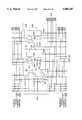
- FIG. 1is a simplified block diagram of a core architecture according to the present invention which may be employed in an FPGA integrated circuit.
- FIG. 2Ais a block/schematic diagram of a presently preferred combinational functional unit according to the present invention, showing a portion of the interconnection architecture of the present invention.
- FIG. 2Bis a table showing the output states of the combinatorial functional unit of FIG. 2A as a function of the states of the inputs.
- FIG. 2Cis a block/schematic diagram of a presently preferred sequential functional unit according to the present invention, showing a portion of the interconnection architecture of the present invention.
- FIGS. 3A-3Hare block/schematic diagrams of other exemplary combinational functional units which may be employed in FPGA architectures according to the present invention.
- FIG. 4Ais a block/schematic diagram of one presently preferred logic module according to the present invention comprising a combination of the functional units of FIGS. 2A and 2C.
- FIGS. 4B-4Dare schematic representations of layout arrangements for logic function units within logic modules connected by local interconnect channels according to the present invention.
- FIG. 1a simplified block diagram of an FPGA core architecture 10 according to the present invention is shown.
- core architecturerefers to the architecture of the core of an FPGA array which comprises a plurality of logic function circuits or modules (reference numerals 12-1 to 12-12) arranged in a matrix with an overlay of interconnect architecture including interconnect conductors and user-programmable interconnect elements.
- the logic function modules 12-1 through 12-12may comprise. any of a variety of circuits, either combinational logic, sequential logic, or combinations thereof, and need not be identical, as will be disclosed in more detail herein with respect to a presently preferred embodiment of the invention.
- logic function modules 12-1 through 12-12are disposed in a network of interconnect conductors.
- the network of interconnect conductorsis shown in simplified schematic form.
- the architecturemay be a "sea of gates" type architecture where the interconnect conductors actually run directly over, rather than between, the logic function circuits.
- the interconnect conductorswill comprise metal lines in layers disposed over the layers which constitute the logic function circuits.
- Such a "sea of gates” architectureis known in the art and is exemplified by U.S. Pat. No. 5,132,571 to McCollum et al. and permits the fabrication of a more dense array than an architecture in which the interconnect conductors run only between the logic function circuits. While such a “sea of gates” arrangement is preferred, those of ordinary skill in the art will recognize that the principles of the present invention apply equally to both types of architectures as well as hybrid architectures having interconnect conductors both directly above and between the logic function circuits.
- FIG. 1depicts an interconnect architecture comprising a plurality of horizontal and vertical channels of interconnect conductors.
- horizontal channelsare depicted as single lines identified by reference numerals 14-1, 14-2, 14-3, and 14-4
- vertical channelsare depicted as single lines identified by reference numerals 16-1, 16-2, 16-3, and 16-4.
- each channelwill comprise a plurality of individual interconnect conductors, some of which may be segmented and some of which may run the length (or width) of the array.
- the number of interconnect conductors present in each channel in any actual integrated circuit which embodies the present inventionwill be dictated by individual design choice, based upon such factors as array size and density.
- segmentation of interconnect conductorsis known and is exemplified in prior art patents such as U.S. Pat. No. 4,758,745 to El Gamal et al. and U.S. Pat. No. 5,073,729 to Greene et al. and is thus not shown in FIG. 1 to avoid over complicating the figure.
- any one of the many available segmentation schemesmay be employed in the architecture of the present invention.
- Such skilled personswill recognize that the segmented interconnect conductors may be selectively joined to make longer conductors by programming user-programmable interconnect elements between selected ones of the conductors.
- intersections of selected ones of the individual conductors horizontal and vertical interconnect channelsare populated with user programmable interconnect elements which may be programmed by the user to make electrical connections between selected ones of them to implement connection nets between the inputs and the outputs of the logic function circuits.
- Groups of such user programmable interconnect elements at the intersections of the horizontal and vertical interconnect channelsare shown schematically in FIG. 1 as squares 18-1 through 18-16.
- Inputs and outputs of the logic function circuitsare also connectable to selected ones of the interconnect conductors in the channels by user-programmable interconnect elements disposed at the intersections of the individual inputs and outputs and selected ones of the interconnect conductors in the channels, as shown schematically by squares 20.
- An important feature of the present inventionis a network of "local interconnect" channels which are shown running between adjacent pairs of logic function circuits in the matrix.
- these local interconnect channelsare shown running between 12-1 and 12-2, 12-3 and 12-4, 12-5 and 12-6, 12-7 and 12-8, 12-9 and 12-10, 12-11 and 12-22, and are indicated by reference numerals 22-1 through 22-6.
- the local interconnect channelsprovide an enhanced interconnection capability between neighboring logic function circuits.
- the local interconnect channelsmay connect more than a single pair of adjacent logic modules.
- local interconnect channel 22-1could also be used in conjunction with the general interconnect channels to make connections to logic modules 12-5 and 12-6 as will be seen more clearly from FIG. 2A.
- selected ones of the individual local interconnect conductorsare connectable to selected ones of the interconnect conductors in the channels by user-programmable interconnect elements placed at intersections thereof.
- the networks of these user-programmable interconnect elementsare shown schematically in FIG. 1 as squares 24.
- I/O modules 26-1, 26-2, 26-3, and 26-4are shown coupled between I/O pads 28-1, 28-2, 28-3, and 28-4, respectively, and horizontal interconnect channels 14-2 and 14-3 and vertical interconnect channels 162 and 16-3 respectively.
- I/O modules 26-1, 26-2, 26-3, and 26-4each comprise an input buffer, an output buffer and input/output function select circuitry.
- the design of particular I/O module circuitryis simply a matter of design choice and is well within the level of ordinary skill in the art. Known examples of such circuitry may be found in United States Pat. No. 5,083,083.
- Program and test control circuit 30contains the necessary circuitry to accept programming data and control signals from off chip via I/O pads 32, 34, and 36. Those of ordinary skill in the art will recognize that the number of such I/O pads necessary for any actual implementation of the present invention will vary according to design choice and requirements.
- the data and control signalsare used to program selected ones of the user-programmable interconnect elements in the integrated circuit in order to define the circuit functions of the logic function modules 12-1 through 12-12 and the I/O modules 26-1 through 26-4 and the circuit connection paths between them.
- Program and test control circuit 30may also be used to provide test data to and obtain test data from the logic function modules 12-1 through 12-12 as known in the art. Examples of testing using such circuitry are found in U.S. Pat. Nos. 4,758,745 and 5,083,083.
- a presently preferred embodiment of combinatorial unit 40 for the programmable logic modulemay comprise three two-input multiplexers 42, 44, and 46.
- First two-input multiplexer 42has a first data input connected to a first data input node 48, a second data input connected to a second data input node 50, a control input connected to the output of a first gate 52, and an output 54.
- the first gate 52has a first input connected to a first control input node 56 and a second input connected to a second control input node 58.
- Second two-input multiplexer 44has a first data input connected to a third data input node 60, a second data input connected to a fourth data input node 62, a control input connected to the output of the first gate 52, and an output 66.
- Third two-input multiplexer 46has a first data input connected to the output 54 of first multiplexer 42, a second data input connected to the output 66 of second multiplexer 44, a control input connected to the output of a second gate 68, and an output 70.
- the second gate 68has a first input connected to a third control input node 72 and a second input connected to a fourth control input node 74.
- An output buffer 76is connected to the output 70 of third multiplexer 46.
- First gate 52 and second gate 68are shown as an AND and an OR gate, respectively, but persons of ordinary skill in the art will recognize that other gate combinations are possible.
- a plurality of interconnect conductors 78, 80, 82, 84, and 86intersect the first through fourth data input nodes 48, 50, 60 and 62 and user-programmable interconnect elements (shown as hollow circles in the drawing figures) are preferably disposed at each intersection to allow programmable connections to be made between selected ones of the interconnect conductors and selected ones of the first through fourth data input nodes.
- Selected ones of the user-programmable interconnect elementsare indicated by reference numerals 88a-88d and will be discussed later with reference to FIG. 2B.
- One of the plurality of interconnect conductors 86is connected to another one of the interconnect conductors 84 through an inverter 90.
- inverter 90adds to the versatility of the logic function module circuits by allowing a selected ones of the data inputs to be inverted. This versatility could be further increased by extending interconnect conductor 86 to cross other functional unit inputs in the same functional unit or by making it a part of the local interconnect channel to allow connections to other functional units.
- the output of inverter 90can also be connected to any of the inputs of gates 52 and 68 through additional antifuses.
- the interconnect conductors 78, 80, 82, and 84are shown intersecting horizontal interconnect conductors 92, 94, 96, and 98 in an upper general interconnect channel and horizontal interconnect conductors 100, 102, 104, and 106 in a lower general interconnect channel.
- the control input nodes 56, 58, 72, and 74 of the first and second gates 52 and 68also cross the horizontal interconnect conductors 92, 94, 96, 98, 100, 102, 104, and 106.
- Other user-programmable interconnect elementsare disposed at the intersections of these conductors and may be programmed to selectively make connections as is known in the art.
- FIG. 2Ais merely illustrative and that other arrangements using other numbers of interconnect conductors and other schemes for populating the conductor intersections with user-programmable interconnect elements are possible.
- the combinatorial unit 40 for the programmable logic module depicted in FIG. 2Ais a compact and flexible circuit, capable of performing a wide variety of combinatorial logic functions.
- FIG. 2Ba table is presented showing the output states of the combinatorial logic function module block of FIG. 2A as a function of the states of its inputs for a small sampling of the available combinatorial functions possible using this unit.
- Those of ordinary skill in the artwill be readily able to determine the remaining possible functions. Such skilled persons will also readily recognize that multiple implementations are possible for certain of these functions. In reading the Table of FIG.
- A0 and B0represent the first and second control inputs 56 and 58 of AND Gate 52
- A1 and B1represent the first and second control inputs 72 and 74 of OR Gate 68.
- the input lines L0, L1, L2, and L3represent interconnect conductors 78, 80, 82, and 84, respectively.
- the inputs D0, D1, D2, and D3represent the data input nodes 48, 50, 60 and 62, respectively, of the first and second multiplexers 42 and 44.
- the notation IL3 in the entries under "Internal"represent the output of inverter 90 on interconnect conductor 86.
- the entries in FIG. 2Bare straightforward.
- the input terms “a” and “b”are presented to the first and second inputs of AND gate 52 on lines 56 and 58.
- the input term “c”is presented to one of the inputs 72 of OR gate 68 and a logic “0” is presented to the other input 74 of OR gate 68.
- Logic "0" levelsare presented to interconnect conductors 78, 80, and 82, and the input term "d” is presented to interconnect conductor 84.
- D0first data input node 48 to first input of first multiplexer 42
- interconnect conductor 78This may be accomplished by programming user-programmable interconnect element 88a at the intersection of interconnect conductor 78 and first data input node 48.
- D1second data input node 50 to second input of first multiplexer 42
- interconnect conductor 80This may be accomplished by programming user-programmable interconnect element 88b at the intersection of interconnect conductor 80 and second data input node 50.
- D2third data input node 60 to first input of second multiplexer 44
- the sequential logic unit 110for a logic module according to the present invention is shown in block/schematic format.
- the sequential logic unitcomprises three multiplexers and a D flip-flop.
- a first two-input multiplexer 112has a first data input connected to a first data input node 114, a second data input connected to a second data input node 116, a control input connected to a first control node 118, and an output 120.
- a second two-input multiplexer 122has a first data input connected to the output 120 of the first multiplexer, a second data input connected to the output of D flip-flop 124, a control input connected to a second control node 126, and an output 128 connected to the D input of the D flip-flop 124.
- a first four-input multiplexer 130has a first data input connected to a first clock input node 132, a second data input connected to the complement of the signal on first clock input node 132, a third data input connected to a second clock input at node 134, a fourth data input connected to the complement of the second clock input signal on node 134, a first control input connected to a clock select node 136, a second control input connected to a clock polarity select node 138, and an output 140 connected to the clock input of the D flip-flop 124.
- the output of D flip-flop 124is buffered by buffer 142.
- D flip-flop 124is also provided with set and reset inputs connected to set and reset nodes 144 and 146, respectively.
- sequential unit 110 of FIG. 2Cis connectable to the interconnect architecture of the present invention.
- the various inputs and control inputs of the elements of sequential unit 110are shown intersecting horizontal interconnect conductors 148, 150, 152, and 154, in an upper general interconnect channel and horizontal interconnect conductors 156, 158, 160, and 162 in a lower general interconnect channel.
- User-programmable interconnect elementsare disposed at the intersections of these conductors and may be programmed to selectively make connections as is known in the art.
- sequential unit 110is also a flexible circuit.
- First four-input multiplexer 130is used to select and control the clock source so that the D flip-flop 124 can be driven from a system clock at first clock input node 132, which would preferably be common to all such units on an integrated circuit, or a clock signal from a clock node derived from other signals presented on second clock node 134 from the general interconnect channels.
- the connection of clock polarity select node 138 to first four-input multiplexer 130allows selection of rising or falling edge triggering for the D flip-flop 124.
- this functionis also easily implemented by a third two-input multiplexer and an exclusive-OR gate.
- interconnect conductors 92, 94, 96, 98, 100, 102, 104, 106, 148, 150, 152, 154, 156, 158, 160, and 162these interconnect conductors are local interconnect shared between neighboring logic modules.
- the outputs of the combinatorial unit 40 and the sequential unit 110are hardwired to individual ones of the local interconnect conductors.
- the local interconnect conductorsare given the same reference numerals in FIGS. 2A and 2C.
- four local interconnect conductors 164, 166, 168, and 170are shown, although those of ordinary skill in the art will recognize that the number of local interconnect conductors to be used in any actual realization of the architecture of the present invention will be largely a matter of design choice and the number of combinational and sequential units in the locally interconnected logic modules.
- the output of buffer 76 of combinatorial unit 40is shown hardwired to local interconnect conductor 164.
- the output of buffer 142 of sequential unit 110is shown hardwired to local interconnect conductor 166.
- Selected ones of the other data and control inputs of combinatorial unit 40 and sequential unit 110are shown connectable to local interconnect conductors 164, 166, 168, and 170 via user-programmable interconnect elements shown as circles at the intersections of the data and control inputs of combinatorial unit 40 and sequential unit 110 and local interconnect conductors 164, 166, 168, and 170.
- combinatorial unit 40 of FIG. 2AWhile it is presently preferred to employ the combinatorial unit 40 of FIG. 2A in the present invention, those of ordinary skill in the art will appreciate that other combinatorial units will be usefully employed in the architecture of the present invention. Referring now to FIGS. 3A-3H, alternative combinatorial unit circuits are presented.
- FIG. 3Aan alternative embodiment of a combinatorial unit 180 is shown comprising a single two-input multiplexer 182.
- First two-input multiplexer 182has a first data input connected to a first data input node 184, a second data input connected to a second data input node 186, a control input connected to a control input node 188, and an output 190 connected to an output buffer 192.
- First data input node 184is shown intersecting horizontal interconnect conductors 194, 196, 198, 200 and 202 in an upper general interconnect channel.
- Second data input node 186 and control input node 188are shown intersecting horizontal interconnect conductors 204, 206, 208, 210 and 212 in a lower general interconnect channel.
- An inverter 214is shown with its input connected to an inverter input node 216 and its output connected to inverter output node 218.
- Inverter input node 216intersects horizontal interconnect conductors 194, 196, 198, 200, 202, 204, 206, 208, 210 and 212 and inverter output node 218 intersects first and second data input nodes 186 and 184.
- Each of the intersectionsis preferably populated with a user programmable interconnect element so that selected ones of the horizontal interconnect conductors may be connected to the first and second data input nodes 186 and 184 either directly or through inverter 214 and to control input node 188.
- inverter 214adds to the versatility of the logic function module circuits by allowing selected ones of the data inputs to be inverted.
- user programmable interconnect elementsneed not be present at each intersection.
- FIG. 3Ba prior art embodiment of a combinatorial unit 220 is shown comprising three two-input multiplexers.
- First two-input multiplexer 222has a first data input connected to a first data input node 224, a second data input connected to a second data input node 226, a control input connected to the output of a first gate 228, and an output 230.
- the first gate 228has a first input connected to a first control input node 232 and a second input connected to a second control input node 234.
- Second two-input multiplexer 236has a first data input connected to a third data input node 238, a second data input connected to a fourth data input node 240, a control input connected to the output of the first gate 228, and an output 242.
- Third two-input multiplexer 244has a first data input connected to the output 230 of first two-input multiplexer 222, a second data input connected to the output 242 of second two-input multiplexer 236, a control input connected to the output of a second gate 246, and an output 248 connected to an output buffer 250.
- the second gate 246has a first input connected to a third control input node 252 and a second input connected to a fourth control input node 254.
- First gate 228 and second gate 246are shown as an AND and an OR gate, respectively, but persons of ordinary skill in the art will recognize that other gate combinations are possible. Persons of ordinary skill in the art will also recognize that the first and second gates may be omitted entirely and that the control inputs of the multiplexers can be connected to the a control input node which intersects the horizontal interconnect conductors of a general interconnect channel.
- the first, second and third multiplexers 222, 236 and 244comprise first and second multiplexer planes in a cascaded multiplexer architecture.
- the first and second multiplexers 222 and 236form a first multiplexer plane in which the inputs are connected to input nodes 224, 226, 238 and 240.
- the outputs 230 and 242 of first and second multiplexers 222 and 236feed into the inputs of third multiplexer 244.
- Third multiplexer 244forms a second multiplexer plane in the cascaded multiplexer architecture.
- First and third data input nodes 224 and 238 and first and third control input nodes 232 and 252are shown intersecting horizontal interconnect conductors 256, 258, 260, 262 and 264 in an upper general interconnect channel.
- Second and fourth data input nodes 226 and 240 and second and fourth control input nodes 234 and 254are shown intersecting horizontal interconnect conductors 266, 268, 270, 272 and 274 in a lower general interconnect channel.
- Each of the intersectionsis preferably populated with a user programmable interconnect element so that selected ones of the horizontal interconnect conductors may be connected to the first through fourth data input nodes 224, 226, 238 and 240 and first through fourth control input nodes 232, 234, 252 and 254.
- user programmable interconnect elementsneed not be present at each intersection.
- FIG. 3Canother embodiment of a combinatorial unit 280 is shown.
- the embodiment shown in FIG. 3Cdiffers from that shown in FIG. 3B in that an inverter 282 is shown which increases the versatility of the combinatorial unit 280.
- the inverter 282has its input connected to an input node 284 which intersects horizontal interconnect conductors 256, 258, 260, 262, 264, 266, 268, 270, 272 and 274.
- the output of inverter 282is connected to an output node 286 which intersects first through fourth data input nodes 224, 226, 238 and 240.
- Each of the intersectionsis preferably populated with a user programmable interconnect element so that selected ones of the horizontal interconnect conductors may be connected to the inverter input node 284 and that selected ones of the data input nodes 224, 226, 238 and 240 may be connected to the inverter output node 286.
- user programmable interconnect elementsneed not be present at each intersection.
- FIG. 3Danother alternative embodiment of a combinatorial unit 290 is shown comprising three two-input multiplexers and two two-input control multiplexers.
- First two-input multiplexer 292has a first data input connected to a first data input node 294, a second data input connected to a second data input node 296, a control input connected to the output of a first two-input control multiplexer 298 and an output 300.
- Second two-input multiplexer 302has a first data input connected to a third data input node 304, a second data input connected to a fourth data input node 306, a control input connected to the output of first two-input control multiplexer 298 and an output 308.
- the first two-input control multiplexer 298has an input connected to a first input control node 310, an inverting input connected to a second input control node 312 and a control input connected to a first input control multiplexer node 314.
- Third two-input multiplexer 316has a first data input connected to the output 300 of first two-input multiplexer 292, a second data input connected to the output 308 of second two-input multiplexer 302, a control input connected to the output of second two-input control multiplexer 318 and an output 320 connected to an output buffer 322.
- the second two-input control multiplexer 318has an inverting input connected to a third input control node 324, an input connected to a fourth input control node 326 and a control input connected to a second input control multiplexer node 328.
- the first, second and third multiplexers 292, 302 and 316comprise a cascaded multiplexer architecture in which first and second multiplexers 292 and 302 form a first multiplexer plane and third multiplexer 316 forms a second multiplexer plane.
- First and third data input nodes 294 and 304, first and third input control nodes 310 and 324 and second input control multiplexer node 328are shown intersecting horizontal interconnect conductors 330, 332, 334, 336 and 338 in an upper general interconnect channel.
- Second and fourth data input nodes 296 and 306, second and fourth input control nodes 312 and 326 and first input control multiplexer node 314are shown intersecting horizontal interconnect conductors 340, 342, 344, 346 and 348 in a lower general interconnect channel.
- Each of the intersectionsis preferably populated with a user programmable interconnect element so that selected ones of the horizontal interconnect conductors may be connected to the first through fourth data input nodes 294, 296, 304 and 306, first through fourth input control nodes 310, 312, 324 and 326, and first and second input control multiplexer nodes 314 and 328.
- user programmable interconnect elementsneed not be present at each intersection.
- FIG. 3Ean alternative embodiment of a logic function module 350 is shown in which a single four-input multiplexer 352 is employed instead of the three two-input cascaded multiplexer architecture shown in FIGS. 3B, 3C and 3D.
- a single four-input multiplexer 352is employed instead of the three two-input cascaded multiplexer architecture shown in FIGS. 3B, 3C and 3D.
- multiplexersmay be employed to implement the four-input logic function modules shown in FIGS. 3B through 3E.
- FIG. 3Fanother alternative embodiment of a combinatorial unit 360 is shown comprising seven two-input multiplexers.
- First through fourth two-input multiplexers 362, 364, 366 and 368each have first and second data inputs connected respectively to first through eighth data inputs nodes 370, 372, 374, 376, 378, 380, 382 and 384, have outputs 386, 388, 390 and 392, respectively, and each have a control input connected to first input control node 394 as shown in FIG. 3F.
- Fifth and sixth two-input multiplexers 396 and 398each have first and second data inputs connected respectively to the outputs 386, 388, 390 and 392, have outputs 400 and 402, respectively, and each have a control input connected to the output of first gate 404.
- the first gate 404has a first input connected to a second control input node 406 and a second input connected to a third control input node 408.
- Seventh two-input multiplexer 410has a first data input connected to the output 400 of fifth two-input multiplexer 396, a second data input connected to the output 402 of sixth two-input multiplexer 398, a control input connected to the output of a second gate 412, and an output 414 connected to an output buffer 416.
- the second gate 412has a first input connected to a fourth control input node 418 and a second input connected to a fifth control input node 420.
- First gate 404 and second gate 412are shown as an AND and an OR gate, respectively, but persons of ordinary skill in the art will recognize that other gate combinations are possible.
- the first through seventh multiplexers 362, 364, 366, 368, 396, 398 and 410comprise a cascaded multiplexer architecture in which first, second, third and fourth multiplexers 362, 364, 366 and 368 form a first multiplexer plane, fifth and sixth multiplexers 396 and 398 form a second multiplexer plane and seventh multiplexer 410 forms a third multiplexer plane.
- a plurality of interconnect conductors 422, 424, 426, 428, and 430intersect the first through eighth data input nodes 370, 372, 374, 376, 378, 380, 382 and 384 and each of the intersections is preferably populated with a user programmable interconnect element and may be programmed to selectively make connections between selected ones of the interconnect conductors and selected ones of the first through eighth data input nodes as is known in the art. Those of ordinary skill in the will appreciate that user programmable interconnect elements need not be present at each intersection.
- One of the plurality of interconnect conductors 430is connected to another one of the interconnect conductors 428 through an inverter 432.
- inverter 432adds to the versatility of the logic function module circuits by allowing selected ones of the data inputs to be inverted.
- interconnect conductors 422, 424, 426, 428, and 430to connect the input nodes 370, 372, 374. 376, 378, 380, 382 and 384 to the general interconnect channel provides several distinct advantages over directly intersecting the data input nodes with the general interconnect channels as shown in FIGS. 3A-3E. First, it reduces capacitive loading of the net being programmed which provides enhanced circuit performance. Second, there is greater symmetry and flexibility in connecting inputs to the general interconnect channels.
- interconnect conductors 78a-86a shown in FIG. 2Ahave the same advantages as recited for the interconnect conductors 422, 424, 426, 428, and 430 in FIG. 3F.
- the interconnect conductors 422 and 426 and the second and fourth control inputs 406 and 418are shown intersecting horizontal interconnect conductors 434, 436, 438, 440 and 442 in an upper general interconnect channel.
- the interconnect conductors 424 and 428 and the first, third and fifth control inputs 394, 408 and 420are shown intersecting horizontal interconnect conductors 444, 446, 448, 450 and 452 in a lower general interconnect channel.
- Each of the intersectionsis preferably populated with a user programmable interconnect element and may be programmed to selectively make connections as is known in the art. Those of ordinary skill in the will appreciate that user programmable interconnect elements need not be present at each intersection.
- FIG. 3Ga sixth alternative embodiment of a combinatorial unit 460 is shown comprising eight two-input multiplexers.
- First through fourth two-input multiplexers 462, 464, 466 and 468each have first and second data inputs connected respectively to first through eighth data inputs nodes 470, 472, 474, 476, 478, 480, 482 and 484, have outputs 486, 488, 490 and 492, respectively, and each have a control input connected to first input control node 494 as shown in FIG. 3H.
- Fifth and sixth two-input multiplexers 496 and 498each have first and second data inputs connected respectively to the outputs 486, 488, 490 and 492, have outputs 500 and 502, respectively, and each have a control input connected to the output of first gate 504.
- the first gate 504has a first input connected to a second control input node 506 and a second input connected to a third control input node 508.
- Seventh two-input multiplexer 510has a first data input connected to the output 500 of fifth two-input multiplexer 496, a second data input connected to the output 502 of sixth two-input multiplexer 498, a control input connected to the output of a second gate 512, and an output 514.
- the second gate 512has a first input connected to a fourth control input node 516 and a second input connected to a fifth control input node 518.
- First gate 504 and second gate 512are shown as an AND and an OR gate, respectively, but persons of ordinary skill in the art will recognize that other gate combinations are possible.
- Eighth two-input multiplexer 520has first and second data inputs connected to a ninth and tenth data input nodes 522 and 524, respectively, a control input connected to the output 514 of seventh two-bit multiplexer 510, and an output 526 connected to an output buffer 528.
- the first through seventh multiplexers 462, 464, 466, 468, 496, 498 and 510comprise a cascaded multiplexer architecture in which first, second, third and fourth multiplexers 462, 464, 466 and 468 form a first multiplexer plane, fifth and sixth multiplexers 496 and 498 form a second multiplexer plane and seventh multiplexer 510 forms a third multiplexer plane.
- user programmable interconnect elementsneed not be present at each intersection.
- Each of the interconnect conductors 538 and 542are also connected to interconnect conductors 536 and 540 through inverters 544 and 546, respectively.
- inverters 544 and 546adds to the versatility of the logic function module circuits by allowing a selected ones of the data inputs to be inverted.
- interconnect conductors 530, 532, 534, 536, 538, 540 and 542reduces capacitive loading, provides greater symmetry and flexibility and limits the required number of general interconnect channels.
- the interconnect conductors 530 and 534 and the second and fourth control inputs 506 and 516are shown intersecting horizontal interconnect conductors 548, 550, 552, 554 and 556 in an upper general interconnect channel.
- the interconnect conductors 532, 536 and 540 and the first, third and fifth control inputs 504, 508 and 518are shown intersecting horizontal interconnect conductors 558, 560, 562, 564 and 566 in a lower general interconnect channel.
- Each of the intersectionsis preferably populated with a user programmable interconnect element and may be programmed to selectively make connections as is known in the art. Those of ordinary skill in the will appreciate that user programmable interconnect elements need not be present at each intersection.
- the first multiplexer plane in both FIGS. 3F and 3Gmay comprise various arrangements of multiplexers, for example, a single four-input multiplexer and two two-input multiplexers connected to eight input nodes.
- the second multiplexer planecould then be a single two-input multiplexer with inputs connected to the outputs of the two two-input multiplexers from the first plane.
- the third planecould then be a single two-input multiplexer with inputs connected to the four-input multiplexer of the first plane and the two-input multiplexer of the second plane.
- the outputs of the multiplexers in a multiplexer planedo not necessarily have to be connected to the inputs of the multiplexers in the next immediately successive multiplexer plane.
- FIG. 3Han alternative embodiment of the logic function module 570 is shown in which a single eight-input multiplexer 572 is employed instead of the seven two-input cascaded multiplexer architecture shown in FIGS. 3F and 3G.
- a single eight-input multiplexer 572is employed instead of the seven two-input cascaded multiplexer architecture shown in FIGS. 3F and 3G.
- multiplexersmay be employed to implement the eight-input logic function modules shown in FIGS. 3F through 3H.
- Local interconnect conductorsare not shown for the alternative embodiments of the combinatorial units 180, 220, 280, 290, 350, 360, 460 and 570 in FIGS. 3A-3H to avoid over complicating the disclosure.
- One of ordinary skill in the artwill recognize that as shown in the illustrative embodiments shown in FIGS. 2A and 2C, selected ones of the data and control inputs shown in the combinatorial units 180, 220, 280, 290, 350, 360, 460 and 570 in FIGS. 3A-3H may be connected to local interconnect conductors.
- FIGS. 3A-3Hshow structures with four and eight inputs into the first multiplexer plane, those of ordinary skill in the art will readily recognize that the invention disclosed herein is not so limited.
- the cascaded multiplexer architecture described hereinis not limited by the number of inputs to the first multiplexer plane, nor the number of planes present in the cascaded multiplexer architecture.
- the logic modulemay comprise three combinatorial units or three sequential units, or may be mixed, i.e., the logic module may comprise one combinatorial unit and two sequential units.
- the logic modulemay be advantageous to internally connect the prebuffered output of the combinatorial unit to one of the inputs of the first multiplexer of the sequential unit. Such an arrangement is shown in FIG. 4A.
- logic function module 600is depicted in block/schematic format.
- logic function module 600is shown to include a combinatorial unit 40 and two sequential units 110a and 110b.
- the elements of these units depicted in FIG. 4Awill be referred to using the same reference numerals used in FIGS. 2A and 2C, although not all elements are numbered in FIG. 4A to avoid overcrowding the drawing.
- An upper general interconnect channelincludes general interconnect conductors 602, 604, 606, 608, and 610, some of which may be dedicated to clock signal and dedicated logic level functions, and a lower general interconnect channel includes general interconnect conductors 612, 614, 616, 618, and 620, some of which may also be dedicated to clock signal and dedicated logic level functions.
- a local interconnect channel 622includes local interconnect conductors 624, 626, 628, 630, 632 and 634.
- the output of output buffer 76 of combinatorial unit 40is shown hardwired to local interconnect conductor 624.
- the output of output buffer 142a of combinatorial unit 110ais shown hardwired to local interconnect conductor 626.
- output buffer 142b of combinatorial unit 110bis shown hardwired to local interconnect conductor 628.
- an internal hardwired connectionis shown made between the pre-buffered output of combinatorial unit 40 and the first input 114a of multiplexer 112a in sequential unit 110a.
- the pre-buffered output of combinatorial unit 40can be hardwired to the control input of multiplexer 112a.
- the logic function module of FIG. 4Ais extremely flexible and permits implementation of a wide variety of combinatorial and sequential logic functions.
- the advantage of the local interconnect channelbecomes apparent.
- the outputs of the combinatorial and sequential elementsare individually hardwired to different ones of local interconnect conductors 624, 626, 628, 630, 632, and 634. Because the hardwired connections bypass any user-programmable interconnect elements in the general interconnect channels, any time delay which such interconnect elements will normally introduce to signals passing through them are eliminated, resulting in a circuit which is, in effect, a larger, faster, single logic function module.
- FIG. 4Aalso illustrates the extra versatility which the addition of inverter 90 of FIG. 2A adds to the logic module function.
- the inverter 90 shown physically located in the combinatorial unit 40may be used with the combinatorial unit 40 or with either sequential unit 110a and 110b by programming appropriate antifuses to connect its output to the data inputs and control inputs of the data multiplexers 112a and 122a associated with sequential unit 110a and 112b and 122b associated with sequential unit 110b and to the set and reset inputs of the D flip-flops 124a and 124b in the sequential units 110a and 110b, respectively.
- the mixture and placement of the combinatorial and sequential components of pairs of logic functionmay be advantageously varied.
- This aspect of the inventionis illustrated in FIGS. 4B-4D, schematic representations of the layouts of logic function module pairs connected by local interconnect channels according to the present invention.
- a logic function module paircomprising logic function modules 600a and 600b are shown connected by local interconnect bus 622a.
- Logic function module 600acomprises a leftmost combinatorial unit 640, a center sequential unit 642, and a rightmost combinatorial unit 644.
- Logic function module 600bcomprises a leftmost combinatorial unit 646, a center sequential unit 648, and a rightmost combinatorial unit 650.
- FIGS. 4C and 4DOther variations of the logic module pair layout according to the present invention are shown in FIGS. 4C and 4D.
- a logic function module paircomprising logic function modules 600c and 600d are shown connected by local interconnect bus 622b.
- Logic function module 600ccomprises a leftmost combinatorial unit 652, a center sequential unit 654, and a rightmost combinatorial unit 656.
- Logic function module 600dcomprises a leftmost sequential unit 658, a center sequential unit 660, and a rightmost combinatorial unit 662.
- FIG. 4Da logic function module pair comprising logic function modules 600e and 600f are shown connected by local interconnect bus 622c.
- Logic function module 600ecomprises a leftmost combinatorial unit 664, a center sequential unit 666, and a rightmost sequential unit 668.
- Logic function module 600fcomprises a leftmost combinatorial unit 670, a center sequential unit 672, and a rightmost combinatorial unit 674.
- the interconnect conductors of the interconnect architecture of the present inventionmay be supplied as segments.
- the ability to temporarily connect the segments together for purposes such as testingmay be provided.
- user-programmable interconnect elementsmay be provided to programmably connect the segments together to produce longer interconnect conductors during normal operation of the integrated circuit.
- each of interconnect conductors 78, 80, 82, 84, and 86are divided into segments by pass transistors.
- interconnect conductor 78is connected to one of the source/drain terminals of pass transistor 700.
- the other source/drain terminal of pass transistor 700is connected to interconnect conductor 78a, which may be considered as a downwardly extending vertical extension of interconnect conductor 78.
- interconnect conductor 80is connected to one of the source/drain terminals of pass transistor 702.
- the other source/drain terminal of pass transistor 702is connected to interconnect conductor 80a, which. may be considered as an upwardly extending vertical extension of interconnect conductor 80.
- Interconnect conductor 82is connected to one of the source/drain terminals of pass transistor 704.
- the other source/drain terminal of pass transistor 704is connected to interconnect conductor 82a, which may be considered as a downwardly extending vertical extension of interconnect conductor 82.
- Interconnect conductor 84is connected to one of the source/drain terminals of pass transistor 706.
- the other source/drain terminal of pass transistor 706is connected to interconnect conductor 84a, which may be considered as an upwardly extending vertical extension of interconnect conductor 84.
- Interconnect conductor 86is connected to one of the source/drain terminals of pass transistor 708.
- the other source/drain terminal of pass transistor 708is connected to interconnect conductor 86a, which may be considered as an upwardly extending vertical extension of interconnect conductor 86.
- the locations of the pass transistorsare preferably staggered to add to the versatility of the interconnect architecture.
- pass transistors 700 and 704are located at one vertical position on their associated interconnect conductors while pass transistors 702, 706, and 708 are located at another vertical position on their associated interconnect conductors.
- the gates of the pass transistorsare driven by the program and test control circuit 30 (FIG. 1 ). While the gates of pass transistors 700 and 704 are shown connected to a common gate line 710 and the gates of pass transistors 702, 706, and 708 are shown connected to a common gate line 712, those of ordinary skill in the art will recognize that other arrangements are possible.
- interconnect conductors 78a and 82awill be connectable through user-programmable interconnect elements to the logic module (not shown in FIG. 2A) located below logic module in the integrated circuit array and that interconnect conductors 80a, 84a, and 86a will be connectable through user-programmable interconnect elements to the logic module (not shown in FIG. 2A) located above logic module in the integrated circuit array.
- the particular segmentation scheme used in an actual architecture fabricated according to the present inventionwill be somewhat arbitrary and largely a matter of design choice dictated by the particular architectural layout.
Landscapes
- Physics & Mathematics (AREA)
- Engineering & Computer Science (AREA)
- General Engineering & Computer Science (AREA)
- Mathematical Physics (AREA)
- Computer Hardware Design (AREA)
- General Physics & Mathematics (AREA)
- Computing Systems (AREA)
- Microelectronics & Electronic Packaging (AREA)
- Logic Circuits (AREA)
- Design And Manufacture Of Integrated Circuits (AREA)
Abstract
Description
Claims (81)
Priority Applications (2)
| Application Number | Priority Date | Filing Date | Title |
|---|---|---|---|
| US08/522,945US5606267A (en) | 1986-09-19 | 1995-09-01 | Programmable logic module and architecture for field programmable gate array device |
| US08/746,554US5698992A (en) | 1986-09-19 | 1996-11-13 | Programmable logic module and architecture for field programmable gate array device |
Applications Claiming Priority (8)
| Application Number | Priority Date | Filing Date | Title |
|---|---|---|---|
| US06909261US4758745B1 (en) | 1986-09-19 | 1986-09-19 | User programmable integrated circuit interconnect architecture and test method |
| US07195728US4873459B1 (en) | 1986-09-19 | 1988-05-18 | Programmable interconnect architecture |
| US07/621,452US5172014A (en) | 1986-09-19 | 1991-01-15 | Programmable interconnect architecture |
| US07/869,488US5187393A (en) | 1986-09-19 | 1992-04-15 | Reconfigurable programmable interconnect architecture |
| US08/002,873US5367208A (en) | 1986-09-19 | 1993-01-13 | Reconfigurable programmable interconnect architecture |
| US08/246,218US5451887A (en) | 1986-09-19 | 1994-05-19 | Programmable logic module and architecture for field programmable gate array device |
| US08/332,550US5477165A (en) | 1986-09-19 | 1994-12-28 | Programmable logic module and architecture for field programmable gate array device |
| US08/522,945US5606267A (en) | 1986-09-19 | 1995-09-01 | Programmable logic module and architecture for field programmable gate array device |
Related Parent Applications (2)
| Application Number | Title | Priority Date | Filing Date |
|---|---|---|---|
| US07/309,306DivisionUS5015885A (en) | 1986-09-19 | 1989-02-10 | Reconfigurable programmable interconnect architecture |
| US08/332,550ContinuationUS5477165A (en) | 1986-09-19 | 1994-12-28 | Programmable logic module and architecture for field programmable gate array device |
Related Child Applications (1)
| Application Number | Title | Priority Date | Filing Date |
|---|---|---|---|
| US08/746,554ContinuationUS5698992A (en) | 1986-09-19 | 1996-11-13 | Programmable logic module and architecture for field programmable gate array device |
Publications (1)
| Publication Number | Publication Date |
|---|---|
| US5606267Atrue US5606267A (en) | 1997-02-25 |
Family
ID=23298746
Family Applications (3)
| Application Number | Title | Priority Date | Filing Date |
|---|---|---|---|
| US08/332,550Expired - LifetimeUS5477165A (en) | 1986-09-19 | 1994-12-28 | Programmable logic module and architecture for field programmable gate array device |
| US08/522,945Expired - LifetimeUS5606267A (en) | 1986-09-19 | 1995-09-01 | Programmable logic module and architecture for field programmable gate array device |
| US08/746,554Expired - LifetimeUS5698992A (en) | 1986-09-19 | 1996-11-13 | Programmable logic module and architecture for field programmable gate array device |
Family Applications Before (1)
| Application Number | Title | Priority Date | Filing Date |
|---|---|---|---|
| US08/332,550Expired - LifetimeUS5477165A (en) | 1986-09-19 | 1994-12-28 | Programmable logic module and architecture for field programmable gate array device |
Family Applications After (1)
| Application Number | Title | Priority Date | Filing Date |
|---|---|---|---|
| US08/746,554Expired - LifetimeUS5698992A (en) | 1986-09-19 | 1996-11-13 | Programmable logic module and architecture for field programmable gate array device |
Country Status (7)
| Country | Link |
|---|---|
| US (3) | US5477165A (en) |
| EP (1) | EP0800723A1 (en) |
| JP (1) | JPH10507605A (en) |
| KR (1) | KR100252614B1 (en) |
| AU (1) | AU4405196A (en) |
| CA (1) | CA2197221A1 (en) |
| WO (1) | WO1996020534A1 (en) |
Cited By (18)
| Publication number | Priority date | Publication date | Assignee | Title |
|---|---|---|---|---|
| US5682106A (en)* | 1994-05-20 | 1997-10-28 | Quicklogic Corporation | Logic module for field programmable gate array |
| US5781033A (en) | 1990-05-11 | 1998-07-14 | Actel Corporation | Logic module with configurable combinational and sequential blocks |
| US5784636A (en)* | 1996-05-28 | 1998-07-21 | National Semiconductor Corporation | Reconfigurable computer architecture for use in signal processing applications |
| US5936426A (en) | 1997-02-03 | 1999-08-10 | Actel Corporation | Logic function module for field programmable array |
| US6160420A (en) | 1986-09-19 | 2000-12-12 | Actel Corporation | Programmable interconnect architecture |
| US6275052B1 (en) | 1997-02-11 | 2001-08-14 | Micron Technology, Inc. | Probe card and testing method for semiconductor wafers |
| US6476636B1 (en) | 2000-09-02 | 2002-11-05 | Actel Corporation | Tileable field-programmable gate array architecture |
| US20030186001A1 (en)* | 2001-02-28 | 2003-10-02 | Nazir Khan | Laser coding |
| US20030201795A1 (en)* | 2000-09-02 | 2003-10-30 | Jung-Cheun Lien | Tileable field-programmable gate array architecture |
| US20040132222A1 (en)* | 1997-02-11 | 2004-07-08 | Hembree David R. | Probe card for semiconductor wafers and method and system for testing wafers |
| US6774672B1 (en) | 2002-12-30 | 2004-08-10 | Actel Corporation | Field-programmable gate array architecture |
| US6774670B1 (en) | 2002-12-30 | 2004-08-10 | Actel Corporation | Intra-tile buffer system for a field programmable gate array |
| US6774669B1 (en) | 2002-12-30 | 2004-08-10 | Actel Corporation | Field programmable gate array freeway architecture |
| US6800884B1 (en) | 2002-12-30 | 2004-10-05 | Actel Corporation | Inter-tile buffer system for a field programmable gate array |
| US6937063B1 (en) | 2000-09-02 | 2005-08-30 | Actel Corporation | Method and apparatus of memory clearing with monitoring RAM memory cells in a field programmable gated array |
| US6960935B1 (en) | 2001-12-18 | 2005-11-01 | Actel Corporation | Method and apparatus for cascade programming a chain of cores in an embedded environment |
| US7015719B1 (en) | 2000-09-02 | 2006-03-21 | Actel Corporation | Tileable field-programmable gate array architecture |
| US7426665B1 (en) | 2000-09-02 | 2008-09-16 | Actel Corporation | Tileable field-programmable gate array architecture |
Families Citing this family (43)
| Publication number | Priority date | Publication date | Assignee | Title |
|---|---|---|---|---|
| US5477165A (en)* | 1986-09-19 | 1995-12-19 | Actel Corporation | Programmable logic module and architecture for field programmable gate array device |
| GB9223226D0 (en)* | 1992-11-05 | 1992-12-16 | Algotronix Ltd | Improved configurable cellular array (cal ii) |
| US5594363A (en)* | 1995-04-07 | 1997-01-14 | Zycad Corporation | Logic cell and routing architecture in a field programmable gate array |
| US6028446A (en)* | 1995-06-06 | 2000-02-22 | Advanced Micro Devices, Inc. | Flexible synchronous and asynchronous circuits for a very high density programmable logic device |
| US6114714A (en)* | 1995-11-07 | 2000-09-05 | Gangopadhyay; Shubhra | Antifuse development using α-c:h,n,f thin films |
| US5901279A (en)* | 1996-10-18 | 1999-05-04 | Hughes Electronics Corporation | Connection of spares between multiple programmable devices |
| US6014038A (en)* | 1997-03-21 | 2000-01-11 | Lightspeed Semiconductor Corporation | Function block architecture for gate array |
| US6107825A (en)* | 1997-10-16 | 2000-08-22 | Altera Corporation | Input/output circuitry for programmable logic devices |
| US6611932B2 (en) | 1997-12-05 | 2003-08-26 | Lightspeed Semiconductor Corporation | Method and apparatus for controlling and observing data in a logic block-based ASIC |
| US6223313B1 (en) | 1997-12-05 | 2001-04-24 | Lightspeed Semiconductor Corporation | Method and apparatus for controlling and observing data in a logic block-based asic |
| US6127843A (en)* | 1997-12-22 | 2000-10-03 | Vantis Corporation | Dual port SRAM memory for run time use in FPGA integrated circuits |
| US6370140B1 (en)* | 1998-01-20 | 2002-04-09 | Cypress Semiconductor Corporation | Programmable interconnect matrix architecture for complex programmable logic device |
| US6169416B1 (en) | 1998-09-01 | 2001-01-02 | Quicklogic Corporation | Programming architecture for field programmable gate array |
| US6762621B1 (en)* | 1998-12-31 | 2004-07-13 | Actel Corporation | Programmable multi-standard I/O architecture for FPGAs |
| US6552410B1 (en) | 1999-08-31 | 2003-04-22 | Quicklogic Corporation | Programmable antifuse interfacing a programmable logic and a dedicated device |
| DE19952898A1 (en)* | 1999-11-03 | 2001-05-10 | Behr Gmbh & Co | Device for control of final control element, especially air flap, of heating or air-conditioning installation of car has circuit outside adjusting drive and control part |
| US6819141B1 (en)* | 2000-03-14 | 2004-11-16 | International Business Machines Corporation | High speed, static digital multiplexer |
| US6294927B1 (en)* | 2000-06-16 | 2001-09-25 | Chip Express (Israel) Ltd | Configurable cell for customizable logic array device |
| US6633182B2 (en)* | 2001-09-05 | 2003-10-14 | Carnegie Mellon University | Programmable gate array based on configurable metal interconnect vias |
| US6696856B1 (en) | 2001-10-30 | 2004-02-24 | Lightspeed Semiconductor Corporation | Function block architecture with variable drive strengths |
| US7256612B1 (en) | 2005-06-14 | 2007-08-14 | Xilinx, Inc. | Programmable logic block providing carry chain with programmable initialization values |
| US7265576B1 (en) | 2005-06-14 | 2007-09-04 | Xilinx, Inc. | Programmable lookup table with dual input and output terminals in RAM mode |
| US7804719B1 (en) | 2005-06-14 | 2010-09-28 | Xilinx, Inc. | Programmable logic block having reduced output delay during RAM write processes when programmed to function in RAM mode |
| US7268587B1 (en) | 2005-06-14 | 2007-09-11 | Xilinx, Inc. | Programmable logic block with carry chains providing lookahead functions of different lengths |
| US7375552B1 (en) | 2005-06-14 | 2008-05-20 | Xilinx, Inc. | Programmable logic block with dedicated and selectable lookup table outputs coupled to general interconnect structure |
| US7274214B1 (en) | 2005-06-14 | 2007-09-25 | Xilinx, Inc. | Efficient tile layout for a programmable logic device |
| US7253658B1 (en)* | 2005-06-14 | 2007-08-07 | Xilinx, Inc. | Integrated circuit providing direct access to multi-directional interconnect lines in a general interconnect structure |
| US7276934B1 (en) | 2005-06-14 | 2007-10-02 | Xilinx, Inc. | Integrated circuit with programmable routing structure including diagonal interconnect lines |
| US7482834B2 (en)* | 2006-10-19 | 2009-01-27 | Quicklogic Corporation | Programmable multiplexer |
| CN100553147C (en)* | 2007-04-25 | 2009-10-21 | 中国科学院半导体研究所 | FPGA Logic Block Based on Partial Local Interconnect Structure |
| FR2933826B1 (en)* | 2008-07-09 | 2011-11-18 | Univ Paris Curie | PROGRAMMABLE LOGIC NETWORK, INTERCONNECT SWITCH AND LOGIC UNIT FOR SUCH A NETWORK |
| US8713327B1 (en)* | 2009-02-02 | 2014-04-29 | Xilinx, Inc. | Circuit for and method of enabling communication of cryptographic data |
| US9077341B1 (en)* | 2013-03-14 | 2015-07-07 | Altera Corporation | Programmable matrix for the allocation of communication resources |
| US9465766B1 (en) | 2013-10-29 | 2016-10-11 | Xilinx, Inc. | Isolation interface for master-slave communication protocols |
| US9047474B1 (en) | 2014-02-21 | 2015-06-02 | Xilinx, Inc. | Circuits for and methods of providing isolation in an integrated circuit |
| US9213866B1 (en) | 2014-04-01 | 2015-12-15 | Xilinx, Inc. | Circuits for and methods of preventing unauthorized access in an integrated circuit |
| US9548741B1 (en)* | 2015-07-14 | 2017-01-17 | Technion Research And Development Foundation Ltd. | Memristive akers logic array |
| US9768784B2 (en)* | 2016-01-28 | 2017-09-19 | Altera Corporation | Transformable logic and routing structures for datapath optimization |
| US10312918B2 (en)* | 2017-02-13 | 2019-06-04 | High Performance Data Storage And Processing Corporation | Programmable logic design |
| KR102771901B1 (en) | 2020-06-19 | 2025-02-25 | 삼성전자주식회사 | Semiconductor devices including work function layers |
| KR102788873B1 (en) | 2020-06-24 | 2025-03-31 | 삼성전자주식회사 | Semiconductor device including capping layer |
| KR102820462B1 (en) | 2020-06-24 | 2025-06-16 | 삼성전자주식회사 | Integrate circuit device including gate line |
| CN115542138B (en)* | 2022-10-13 | 2025-07-15 | 中国电子科技集团公司第五十八研究所 | An anti-fuse FPGA internal logic on-chip test circuit |
Citations (69)
| Publication number | Priority date | Publication date | Assignee | Title |
|---|---|---|---|---|
| US3816725A (en)* | 1972-04-28 | 1974-06-11 | Gen Electric | Multiple level associative logic circuits |
| US3818452A (en)* | 1972-04-28 | 1974-06-18 | Gen Electric | Electrically programmable logic circuits |
| US3849638A (en)* | 1973-07-18 | 1974-11-19 | Gen Electric | Segmented associative logic circuits |
| US3987287A (en)* | 1974-12-30 | 1976-10-19 | International Business Machines Corporation | High density logic array |
| US4293783A (en)* | 1978-11-01 | 1981-10-06 | Massachusetts Institute Of Technology | Storage/logic array |
| JPS57111044A (en)* | 1980-12-27 | 1982-07-10 | Fujitsu Ltd | Master-slice type lsi device |
| US4433331A (en)* | 1981-12-14 | 1984-02-21 | Bell Telephone Laboratories, Incorporated | Programmable logic array interconnection matrix |
| EP0162529A1 (en)* | 1984-01-13 | 1985-11-27 | The British Petroleum Company p.l.c. | Amorphous or microcrystalline semiconductor memory device |
| US4642487A (en)* | 1984-09-26 | 1987-02-10 | Xilinx, Inc. | Special interconnect for configurable logic array |
| WO1987002827A1 (en)* | 1985-10-29 | 1987-05-07 | 4C Electronics, Inc. | Programmable integrated crosspoint switch |
| US4677318A (en)* | 1985-04-12 | 1987-06-30 | Altera Corporation | Programmable logic storage element for programmable logic devices |
| US4701922A (en)* | 1984-09-04 | 1987-10-20 | Hitachi, Ltd. | Integrated circuit device |
| US4706208A (en)* | 1985-09-03 | 1987-11-10 | American Telephone And Telegraph Company, At&T Bell Laboratories | Technique for the operational life test of microprocessors |
| US4713557A (en)* | 1984-09-26 | 1987-12-15 | Xilinx, Inc. | Bidirectional buffer amplifier |
| US4717912A (en)* | 1982-10-07 | 1988-01-05 | Advanced Micro Devices, Inc. | Apparatus for producing any one of a plurality of signals at a single output |
| US4742252A (en)* | 1985-03-29 | 1988-05-03 | Advanced Micro Devices, Inc. | Multiple array customizable logic device |
| US4758745A (en)* | 1986-09-19 | 1988-07-19 | Actel Corporation | User programmable integrated circuit interconnect architecture and test method |
| US4758985A (en)* | 1985-02-27 | 1988-07-19 | Xilinx, Inc. | Microprocessor oriented configurable logic element |
| US4763020A (en)* | 1985-09-06 | 1988-08-09 | Ricoh Company, Ltd. | Programmable logic device having plural programmable function cells |
| US4786904A (en)* | 1986-12-15 | 1988-11-22 | Zoran Corporation | Electronically programmable gate array having programmable interconnect lines |
| US4789951A (en)* | 1986-05-16 | 1988-12-06 | Advanced Micro Devices, Inc. | Programmable array logic cell |
| US4821176A (en)* | 1986-03-18 | 1989-04-11 | Stc Plc | Data processing arrangement using an interconnecting network on a single semiconductor chip |
| US4823181A (en)* | 1986-05-09 | 1989-04-18 | Actel Corporation | Programmable low impedance anti-fuse element |
| US4825105A (en)* | 1984-09-28 | 1989-04-25 | Siemens Aktiengesellschaft | Circuit for generation of logic variables, using multiplexes and inverters |
| US4847732A (en)* | 1983-09-15 | 1989-07-11 | Mosaic Systems, Inc. | Wafer and method of making same |
| US4847612A (en)* | 1988-01-13 | 1989-07-11 | Plug Logic, Inc. | Programmable logic device |
| US4857774A (en)* | 1986-09-19 | 1989-08-15 | Actel Corporation | Testing apparatus and diagnostic method for use with programmable interconnect architecture |
| US4870302A (en)* | 1984-03-12 | 1989-09-26 | Xilinx, Inc. | Configurable electrical circuit having configurable logic elements and configurable interconnects |
| US4870300A (en)* | 1986-08-06 | 1989-09-26 | Mitsubishi Denki Kabushiki Kaisha | Standard cell system large scale integrated circuit with heavy load lines passing through the cells |
| US4871930A (en)* | 1988-05-05 | 1989-10-03 | Altera Corporation | Programmable logic device with array blocks connected via programmable interconnect |
| US4903223A (en)* | 1988-05-05 | 1990-02-20 | Altera Corporation | Programmable logic device with programmable word line connections |
| DE3927033A1 (en)* | 1988-08-23 | 1990-03-01 | Seiko Epson Corp | SEMICONDUCTOR ELEMENT AND METHOD FOR THE PRODUCTION THEREOF |
| US4910417A (en)* | 1986-09-19 | 1990-03-20 | Actel Corporation | Universal logic module comprising multiplexers |
| US4912342A (en)* | 1988-05-05 | 1990-03-27 | Altera Corporation | Programmable logic device with array blocks with programmable clocking |
| US4914055A (en)* | 1989-08-24 | 1990-04-03 | Advanced Micro Devices, Inc. | Semiconductor antifuse structure and method |
| US4963768A (en)* | 1985-03-29 | 1990-10-16 | Advanced Micro Devices, Inc. | Flexible, programmable cell array interconnected by a programmable switch matrix |
| US4963770A (en)* | 1987-11-20 | 1990-10-16 | Kawasaki Steel Corporation | Programmable logic device |
| US5001368A (en)* | 1988-12-09 | 1991-03-19 | Pilkington Micro-Electronics Limited | Configurable logic array |
| US5003200A (en)* | 1988-09-20 | 1991-03-26 | Kawasaki Steel Corporation | Programmable logic device having programmable wiring for connecting adjacent programmable logic elements through a single switch station |
| US5015885A (en)* | 1986-09-19 | 1991-05-14 | Actel Corporation | Reconfigurable programmable interconnect architecture |
| US5019736A (en)* | 1986-11-07 | 1991-05-28 | Concurrent Logic, Inc. | Programmable logic cell and array |
| US5023606A (en)* | 1988-01-13 | 1991-06-11 | Plus Logic, Inc. | Programmable logic device with ganged output pins |
| US5055718A (en)* | 1990-05-11 | 1991-10-08 | Actel Corporation | Logic module with configurable combinational and sequential blocks |
| EP0452091A2 (en)* | 1990-04-12 | 1991-10-16 | Actel Corporation | Electrically programmable antifuse element and method of forming it |
| US5073729A (en)* | 1990-06-22 | 1991-12-17 | Actel Corporation | Segmented routing architecture |
| US5083083A (en)* | 1986-09-19 | 1992-01-21 | Actel Corporation | Testability architecture and techniques for programmable interconnect architecture |
| US5122685A (en)* | 1991-03-06 | 1992-06-16 | Quicklogic Corporation | Programmable application specific integrated circuit and logic cell therefor |
| US5132571A (en)* | 1990-08-01 | 1992-07-21 | Actel Corporation | Programmable interconnect architecture having interconnects disposed above function modules |
| US5140193A (en)* | 1990-03-27 | 1992-08-18 | Xilinx, Inc. | Programmable connector for programmable logic device |
| US5144166A (en)* | 1990-11-02 | 1992-09-01 | Concurrent Logic, Inc. | Programmable logic cell and array |
| US5151623A (en)* | 1985-03-29 | 1992-09-29 | Advanced Micro Devices, Inc. | Programmable logic device with multiple, flexible asynchronous programmable logic blocks interconnected by a high speed switch matrix |
| US5171715A (en)* | 1991-11-12 | 1992-12-15 | Actel Corporation | Process for fabricating electrically programmable antifuse element |
| US5172014A (en)* | 1986-09-19 | 1992-12-15 | Actel Corporation | Programmable interconnect architecture |
| US5181096A (en)* | 1990-04-12 | 1993-01-19 | Actel Corporation | Electrically programmable antifuse incorporating dielectric and amorphous silicon interlayer |
| US5185706A (en)* | 1989-08-15 | 1993-02-09 | Advanced Micro Devices, Inc. | Programmable gate array with logic cells having configurable output enable |
| US5187393A (en)* | 1986-09-19 | 1993-02-16 | Actel Corporation | Reconfigurable programmable interconnect architecture |
| US5220213A (en)* | 1991-03-06 | 1993-06-15 | Quicklogic Corporation | Programmable application specific integrated circuit and logic cell therefor |
| US5245227A (en)* | 1990-11-02 | 1993-09-14 | Atmel Corporation | Versatile programmable logic cell for use in configurable logic arrays |
| US5258668A (en)* | 1992-05-08 | 1993-11-02 | Altera Corporation | Programmable logic array integrated circuits with cascade connections between logic modules |
| US5260611A (en)* | 1991-09-03 | 1993-11-09 | Altera Corporation | Programmable logic array having local and long distance conductors |
| US5291079A (en)* | 1992-07-23 | 1994-03-01 | Xilinx, Inc. | Configuration control unit for programming a field programmable gate array and reading array status |
| US5302886A (en)* | 1989-10-04 | 1994-04-12 | University Of Utah Research Foundation | Mechanical/electrical displacement transducer |
| US5313119A (en)* | 1991-03-18 | 1994-05-17 | Crosspoint Solutions, Inc. | Field programmable gate array |
| US5331226A (en)* | 1992-07-23 | 1994-07-19 | Xilinx, Inc. | Logic cell for field programmable gate array having optional input inverters |
| US5365125A (en)* | 1992-07-23 | 1994-11-15 | Xilinx, Inc. | Logic cell for field programmable gate array having optional internal feedback and optional cascade |
| US5400262A (en)* | 1989-09-20 | 1995-03-21 | Aptix Corporation | Universal interconnect matrix array |
| EP0696812A1 (en)* | 1994-08-10 | 1996-02-14 | International Business Machines Corporation | Thermally activated noise immune fuse |
| EP0697708A1 (en)* | 1994-08-10 | 1996-02-21 | Motorola Semiconducteurs S.A. | Semiconductor fuse devices |
| US8451887B2 (en)* | 2010-04-21 | 2013-05-28 | Richtek Technology Corp. | Phase interleaving control method for a multi-channel regulator system |
Family Cites Families (62)
| Publication number | Priority date | Publication date | Assignee | Title |
|---|---|---|---|---|
| US3619583A (en)* | 1968-10-11 | 1971-11-09 | Bell Telephone Labor Inc | Multiple function programmable arrays |
| US3731073A (en)* | 1972-04-05 | 1973-05-01 | Bell Telephone Labor Inc | Programmable switching array |
| US3912914A (en)* | 1972-12-26 | 1975-10-14 | Bell Telephone Labor Inc | Programmable switching array |
| NL7612223A (en)* | 1976-11-04 | 1978-05-08 | Philips Nv | INTEGRATED CIRCUIT. |
| JPS5483341A (en)* | 1977-12-15 | 1979-07-03 | Nec Corp | Digital integrated circuit |
| US4415818A (en) | 1979-01-16 | 1983-11-15 | Nippon Telegraph & Telephone Corp. | Programmable sequential logic circuit devices |
| GB2049958B (en)* | 1979-03-15 | 1983-11-30 | Nippon Electric Co | Integrated logic circuit adapted to performance tests |
| US4293919A (en)* | 1979-08-13 | 1981-10-06 | International Business Machines Corporation | Level sensitive scan design (LSSD) system |
| US4357678A (en)* | 1979-12-26 | 1982-11-02 | International Business Machines Corporation | Programmable sequential logic array mechanism |
| JPH07119789B2 (en)* | 1983-02-04 | 1995-12-20 | 株式会社日立製作所 | Semiconductor integrated circuit device and diagnostic method thereof |
| US4580215A (en)* | 1983-03-08 | 1986-04-01 | Itt Corporation | Associative array with five arithmetic paths |
| US4600846A (en)* | 1983-10-06 | 1986-07-15 | Sanders Associates, Inc. | Universal logic circuit modules |
| JPS60242678A (en)* | 1984-05-17 | 1985-12-02 | Seiko Epson Corp | semiconductor storage device |
| US5015855A (en)* | 1989-04-10 | 1991-05-14 | International Sensor Technology, Inc. | Radiation dosimetry by counting differentially ionized sample areas from heavy charged particle events |
| JPS61221938A (en)* | 1985-03-28 | 1986-10-02 | Toshiba Corp | Sequence circuit |
| US5225719A (en)* | 1985-03-29 | 1993-07-06 | Advanced Micro Devices, Inc. | Family of multiple segmented programmable logic blocks interconnected by a high speed centralized switch matrix |
| US4758746A (en)* | 1985-08-12 | 1988-07-19 | Monolithic Memories, Inc. | Programmable logic array with added array of gates and added output routing flexibility |
| US5075576A (en)* | 1985-11-19 | 1991-12-24 | North American Philips Corporation | Field-programmable logic device with programmable foldback to control number of logic levels |
| US4845633A (en)* | 1985-12-02 | 1989-07-04 | Apple Computer Inc. | System for programming graphically a programmable, asynchronous logic cell and array |
| JPS62159921A (en)* | 1986-01-08 | 1987-07-15 | Sharp Corp | demultiplexer circuit |
| US5451887A (en)* | 1986-09-19 | 1995-09-19 | Actel Corporation | Programmable logic module and architecture for field programmable gate array device |
| US5477165A (en)* | 1986-09-19 | 1995-12-19 | Actel Corporation | Programmable logic module and architecture for field programmable gate array device |
| US4761570A (en)* | 1987-02-12 | 1988-08-02 | Harris Corporation | Programmable logic device with programmable signal inhibition and inversion means |
| US5046035A (en)* | 1987-08-26 | 1991-09-03 | Ict International Cmos Tech., Inc. | High-performance user programmable logic device (PLD) |
| US4868413A (en)* | 1988-04-20 | 1989-09-19 | International Business Machines Corporation | Testable passgate logic circuits |
| US4912339A (en)* | 1988-12-05 | 1990-03-27 | International Business Machines Corporation | Pass gate multiplexer |
| US5489857A (en)* | 1992-08-03 | 1996-02-06 | Advanced Micro Devices, Inc. | Flexible synchronous/asynchronous cell structure for a high density programmable logic device |
| US5231588A (en)* | 1989-08-15 | 1993-07-27 | Advanced Micro Devices, Inc. | Programmable gate array with logic cells having symmetrical input/output structures |
| US5457409A (en)* | 1992-08-03 | 1995-10-10 | Advanced Micro Devices, Inc. | Architecture of a multiple array high density programmable logic device with a plurality of programmable switch matrices |
| US5267187A (en)* | 1990-05-10 | 1993-11-30 | Xilinx Inc | Logic structure and circuit for fast carry |
| US5198705A (en)* | 1990-05-11 | 1993-03-30 | Actel Corporation | Logic module with configurable combinational and sequential blocks |
| US5416367A (en)* | 1991-03-06 | 1995-05-16 | Quicklogic Corporation | Programmable application specific integrated circuit and logic cell therefor |
| US5208490A (en)* | 1991-04-12 | 1993-05-04 | Hewlett-Packard Company | Functionally complete family of self-timed dynamic logic circuits |
| EP0515043A3 (en) | 1991-05-24 | 1993-11-18 | Actel Corp | Direct interconnect for functional circuit module array |
| US5290734A (en)* | 1991-06-04 | 1994-03-01 | Vlsi Technology, Inc. | Method for making anti-fuse structures |
| US5550782A (en) | 1991-09-03 | 1996-08-27 | Altera Corporation | Programmable logic array integrated circuits |
| JPH05252025A (en)* | 1991-10-28 | 1993-09-28 | Texas Instr Inc <Ti> | Logic module and integrated circuit |
| US5270587A (en)* | 1992-01-06 | 1993-12-14 | Micron Technology, Inc. | CMOS logic cell for high-speed, zero-power programmable array logic devices |
| US5521835A (en)* | 1992-03-27 | 1996-05-28 | Xilinx, Inc. | Method for programming an FPLD using a library-based technology mapping algorithm |
| US5254886A (en)* | 1992-06-19 | 1993-10-19 | Actel Corporation | Clock distribution scheme for user-programmable logic array architecture |
| US5386154A (en)* | 1992-07-23 | 1995-01-31 | Xilinx, Inc. | Compact logic cell for field programmable gate array chip |
| KR960003373B1 (en)* | 1992-09-29 | 1996-03-09 | 후지쓰 가부시키가이샤 | Programmable Logic Circuit |
| US5308795A (en)* | 1992-11-04 | 1994-05-03 | Actel Corporation | Above via metal-to-metal antifuse |
| GB9223226D0 (en)* | 1992-11-05 | 1992-12-16 | Algotronix Ltd | Improved configurable cellular array (cal ii) |
| US5357153A (en) | 1993-01-28 | 1994-10-18 | Xilinx, Inc. | Macrocell with product-term cascade and improved flip flop utilization |
| US5302866A (en)* | 1993-03-18 | 1994-04-12 | Xilinx, Inc. | Input circuit block and method for PLDs with register clock enable selection |
| US5483178A (en)* | 1993-03-29 | 1996-01-09 | Altera Corporation | Programmable logic device with logic block outputs coupled to adjacent logic block output multiplexers |
| US5341044A (en)* | 1993-04-19 | 1994-08-23 | Altera Corporation | Flexible configuration logic array block for programmable logic devices |
| US5481206A (en)* | 1993-09-02 | 1996-01-02 | Xilinx, Inc. | Circuit for fast carry and logic |
| US5546018A (en)* | 1993-09-02 | 1996-08-13 | Xilinx, Inc. | Fast carry structure with synchronous input |
| CA2126265A1 (en) | 1993-09-27 | 1995-03-28 | Michael Robert Cantone | System for synthesizing field programmable gate array implementations from high level circuit descriptions |
| US5448185A (en)* | 1993-10-27 | 1995-09-05 | Actel Corporation | Programmable dedicated FPGA functional blocks for multiple wide-input functions |
| KR960002333B1 (en) | 1993-12-23 | 1996-02-16 | 재단법인한국전자통신연구소 | Logic integrated circuit module |
| JP3081754B2 (en) | 1994-06-03 | 2000-08-28 | 株式会社東芝 | Programmable semiconductor integrated circuit |
| KR960003103A (en) | 1994-06-30 | 1996-01-26 | 윌리엄 이. 힐러 | Association Heterogenius Field Programmable Gate Array Logic Module and Formation Method thereof |
| US5465055A (en)* | 1994-10-19 | 1995-11-07 | Crosspoint Solutions, Inc. | RAM-logic tile for field programmable gate arrays |
| US5537341A (en)* | 1995-02-10 | 1996-07-16 | Jonathan Rose | Complementary architecture for field-programmable gate arrays |
| US5594363A (en) | 1995-04-07 | 1997-01-14 | Zycad Corporation | Logic cell and routing architecture in a field programmable gate array |
| US5541530A (en)* | 1995-05-17 | 1996-07-30 | Altera Corporation | Programmable logic array integrated circuits with blocks of logic regions grouped into super-blocks |
| US5552721A (en) | 1995-06-05 | 1996-09-03 | International Business Machines Corporation | Method and system for enhanced drive in programmmable gate arrays |
| US5600263A (en) | 1995-08-18 | 1997-02-04 | Xilinx, Inc. | Configuration modes for a time multiplexed programmable logic device |
| US5583450A (en) | 1995-08-18 | 1996-12-10 | Xilinx, Inc. | Sequencer for a time multiplexed programmable logic device |
- 1994
- 1994-12-28USUS08/332,550patent/US5477165A/ennot_activeExpired - Lifetime
- 1995
- 1995-09-01USUS08/522,945patent/US5606267A/ennot_activeExpired - Lifetime
- 1995-10-27EPEP95942836Apatent/EP0800723A1/ennot_activeCeased
- 1995-10-27AUAU44051/96Apatent/AU4405196A/ennot_activeAbandoned
- 1995-10-27CACA002197221Apatent/CA2197221A1/ennot_activeAbandoned
- 1995-10-27WOPCT/US1995/013891patent/WO1996020534A1/ennot_activeApplication Discontinuation
- 1995-10-27KRKR1019970701218Apatent/KR100252614B1/ennot_activeExpired - Fee Related
- 1995-10-27JPJP8520438Apatent/JPH10507605A/enactivePending
- 1996
- 1996-11-13USUS08/746,554patent/US5698992A/ennot_activeExpired - Lifetime
Patent Citations (75)
| Publication number | Priority date | Publication date | Assignee | Title |
|---|---|---|---|---|
| US3818452A (en)* | 1972-04-28 | 1974-06-18 | Gen Electric | Electrically programmable logic circuits |
| US3816725A (en)* | 1972-04-28 | 1974-06-11 | Gen Electric | Multiple level associative logic circuits |
| US3849638A (en)* | 1973-07-18 | 1974-11-19 | Gen Electric | Segmented associative logic circuits |
| US3987287A (en)* | 1974-12-30 | 1976-10-19 | International Business Machines Corporation | High density logic array |
| US4293783A (en)* | 1978-11-01 | 1981-10-06 | Massachusetts Institute Of Technology | Storage/logic array |
| JPS57111044A (en)* | 1980-12-27 | 1982-07-10 | Fujitsu Ltd | Master-slice type lsi device |
| US4433331A (en)* | 1981-12-14 | 1984-02-21 | Bell Telephone Laboratories, Incorporated | Programmable logic array interconnection matrix |
| US4717912A (en)* | 1982-10-07 | 1988-01-05 | Advanced Micro Devices, Inc. | Apparatus for producing any one of a plurality of signals at a single output |
| US4847732A (en)* | 1983-09-15 | 1989-07-11 | Mosaic Systems, Inc. | Wafer and method of making same |
| EP0162529A1 (en)* | 1984-01-13 | 1985-11-27 | The British Petroleum Company p.l.c. | Amorphous or microcrystalline semiconductor memory device |
| US4870302A (en)* | 1984-03-12 | 1989-09-26 | Xilinx, Inc. | Configurable electrical circuit having configurable logic elements and configurable interconnects |
| US4701922A (en)* | 1984-09-04 | 1987-10-20 | Hitachi, Ltd. | Integrated circuit device |
| US4642487A (en)* | 1984-09-26 | 1987-02-10 | Xilinx, Inc. | Special interconnect for configurable logic array |
| US4713557A (en)* | 1984-09-26 | 1987-12-15 | Xilinx, Inc. | Bidirectional buffer amplifier |
| US4825105A (en)* | 1984-09-28 | 1989-04-25 | Siemens Aktiengesellschaft | Circuit for generation of logic variables, using multiplexes and inverters |
| US4758985A (en)* | 1985-02-27 | 1988-07-19 | Xilinx, Inc. | Microprocessor oriented configurable logic element |
| US4742252A (en)* | 1985-03-29 | 1988-05-03 | Advanced Micro Devices, Inc. | Multiple array customizable logic device |
| US4963768A (en)* | 1985-03-29 | 1990-10-16 | Advanced Micro Devices, Inc. | Flexible, programmable cell array interconnected by a programmable switch matrix |
| US5151623A (en)* | 1985-03-29 | 1992-09-29 | Advanced Micro Devices, Inc. | Programmable logic device with multiple, flexible asynchronous programmable logic blocks interconnected by a high speed switch matrix |
| US4677318A (en)* | 1985-04-12 | 1987-06-30 | Altera Corporation | Programmable logic storage element for programmable logic devices |
| US4706208A (en)* | 1985-09-03 | 1987-11-10 | American Telephone And Telegraph Company, At&T Bell Laboratories | Technique for the operational life test of microprocessors |
| US4763020B1 (en)* | 1985-09-06 | 1997-07-08 | Ricoh Kk | Programmable logic device having plural programmable function cells |
| US4763020A (en)* | 1985-09-06 | 1988-08-09 | Ricoh Company, Ltd. | Programmable logic device having plural programmable function cells |
| WO1987002827A1 (en)* | 1985-10-29 | 1987-05-07 | 4C Electronics, Inc. | Programmable integrated crosspoint switch |
| US4821176A (en)* | 1986-03-18 | 1989-04-11 | Stc Plc | Data processing arrangement using an interconnecting network on a single semiconductor chip |
| US4823181A (en)* | 1986-05-09 | 1989-04-18 | Actel Corporation | Programmable low impedance anti-fuse element |
| US4789951A (en)* | 1986-05-16 | 1988-12-06 | Advanced Micro Devices, Inc. | Programmable array logic cell |
| US4870300A (en)* | 1986-08-06 | 1989-09-26 | Mitsubishi Denki Kabushiki Kaisha | Standard cell system large scale integrated circuit with heavy load lines passing through the cells |
| US5172014A (en)* | 1986-09-19 | 1992-12-15 | Actel Corporation | Programmable interconnect architecture |
| US4758745B1 (en)* | 1986-09-19 | 1994-11-15 | Actel Corp | User programmable integrated circuit interconnect architecture and test method |
| US4873459A (en)* | 1986-09-19 | 1989-10-10 | Actel Corporation | Programmable interconnect architecture |
| US5187393A (en)* | 1986-09-19 | 1993-02-16 | Actel Corporation | Reconfigurable programmable interconnect architecture |
| US5083083A (en)* | 1986-09-19 | 1992-01-21 | Actel Corporation | Testability architecture and techniques for programmable interconnect architecture |
| US4910417A (en)* | 1986-09-19 | 1990-03-20 | Actel Corporation | Universal logic module comprising multiplexers |
| US4873459B1 (en)* | 1986-09-19 | 1995-01-10 | Actel Corp | Programmable interconnect architecture |
| US4758745A (en)* | 1986-09-19 | 1988-07-19 | Actel Corporation | User programmable integrated circuit interconnect architecture and test method |
| US4857774A (en)* | 1986-09-19 | 1989-08-15 | Actel Corporation | Testing apparatus and diagnostic method for use with programmable interconnect architecture |
| US5015885A (en)* | 1986-09-19 | 1991-05-14 | Actel Corporation | Reconfigurable programmable interconnect architecture |
| US5019736A (en)* | 1986-11-07 | 1991-05-28 | Concurrent Logic, Inc. | Programmable logic cell and array |
| US4786904A (en)* | 1986-12-15 | 1988-11-22 | Zoran Corporation | Electronically programmable gate array having programmable interconnect lines |
| US4963770A (en)* | 1987-11-20 | 1990-10-16 | Kawasaki Steel Corporation | Programmable logic device |
| EP0394575A1 (en)* | 1988-01-13 | 1990-10-31 | Xilinx, Inc. | Programmable logic device |
| US4847612A (en)* | 1988-01-13 | 1989-07-11 | Plug Logic, Inc. | Programmable logic device |
| US5023606A (en)* | 1988-01-13 | 1991-06-11 | Plus Logic, Inc. | Programmable logic device with ganged output pins |
| US4912342A (en)* | 1988-05-05 | 1990-03-27 | Altera Corporation | Programmable logic device with array blocks with programmable clocking |
| US4903223A (en)* | 1988-05-05 | 1990-02-20 | Altera Corporation | Programmable logic device with programmable word line connections |
| US4871930A (en)* | 1988-05-05 | 1989-10-03 | Altera Corporation | Programmable logic device with array blocks connected via programmable interconnect |
| DE3927033A1 (en)* | 1988-08-23 | 1990-03-01 | Seiko Epson Corp | SEMICONDUCTOR ELEMENT AND METHOD FOR THE PRODUCTION THEREOF |
| US5003200A (en)* | 1988-09-20 | 1991-03-26 | Kawasaki Steel Corporation | Programmable logic device having programmable wiring for connecting adjacent programmable logic elements through a single switch station |
| US5001368A (en)* | 1988-12-09 | 1991-03-19 | Pilkington Micro-Electronics Limited | Configurable logic array |
| US5185706A (en)* | 1989-08-15 | 1993-02-09 | Advanced Micro Devices, Inc. | Programmable gate array with logic cells having configurable output enable |
| US4914055A (en)* | 1989-08-24 | 1990-04-03 | Advanced Micro Devices, Inc. | Semiconductor antifuse structure and method |
| US5400262A (en)* | 1989-09-20 | 1995-03-21 | Aptix Corporation | Universal interconnect matrix array |
| US5302886A (en)* | 1989-10-04 | 1994-04-12 | University Of Utah Research Foundation | Mechanical/electrical displacement transducer |
| US5140193A (en)* | 1990-03-27 | 1992-08-18 | Xilinx, Inc. | Programmable connector for programmable logic device |
| US5181096A (en)* | 1990-04-12 | 1993-01-19 | Actel Corporation | Electrically programmable antifuse incorporating dielectric and amorphous silicon interlayer |
| EP0452091A2 (en)* | 1990-04-12 | 1991-10-16 | Actel Corporation | Electrically programmable antifuse element and method of forming it |
| US5070384A (en)* | 1990-04-12 | 1991-12-03 | Actel Corporation | Electrically programmable antifuse element incorporating a dielectric and amorphous silicon interlayer |
| US5055718A (en)* | 1990-05-11 | 1991-10-08 | Actel Corporation | Logic module with configurable combinational and sequential blocks |
| US5073729A (en)* | 1990-06-22 | 1991-12-17 | Actel Corporation | Segmented routing architecture |
| US5132571A (en)* | 1990-08-01 | 1992-07-21 | Actel Corporation | Programmable interconnect architecture having interconnects disposed above function modules |
| US5245227A (en)* | 1990-11-02 | 1993-09-14 | Atmel Corporation | Versatile programmable logic cell for use in configurable logic arrays |
| US5144166A (en)* | 1990-11-02 | 1992-09-01 | Concurrent Logic, Inc. | Programmable logic cell and array |
| US5122685A (en)* | 1991-03-06 | 1992-06-16 | Quicklogic Corporation | Programmable application specific integrated circuit and logic cell therefor |
| US5220213A (en)* | 1991-03-06 | 1993-06-15 | Quicklogic Corporation | Programmable application specific integrated circuit and logic cell therefor |
| US5313119A (en)* | 1991-03-18 | 1994-05-17 | Crosspoint Solutions, Inc. | Field programmable gate array |
| US5260611A (en)* | 1991-09-03 | 1993-11-09 | Altera Corporation | Programmable logic array having local and long distance conductors |
| US5171715A (en)* | 1991-11-12 | 1992-12-15 | Actel Corporation | Process for fabricating electrically programmable antifuse element |
| US5258668A (en)* | 1992-05-08 | 1993-11-02 | Altera Corporation | Programmable logic array integrated circuits with cascade connections between logic modules |
| US5365125A (en)* | 1992-07-23 | 1994-11-15 | Xilinx, Inc. | Logic cell for field programmable gate array having optional internal feedback and optional cascade |
| US5331226A (en)* | 1992-07-23 | 1994-07-19 | Xilinx, Inc. | Logic cell for field programmable gate array having optional input inverters |
| US5291079A (en)* | 1992-07-23 | 1994-03-01 | Xilinx, Inc. | Configuration control unit for programming a field programmable gate array and reading array status |
| EP0696812A1 (en)* | 1994-08-10 | 1996-02-14 | International Business Machines Corporation | Thermally activated noise immune fuse |
| EP0697708A1 (en)* | 1994-08-10 | 1996-02-21 | Motorola Semiconducteurs S.A. | Semiconductor fuse devices |
| US8451887B2 (en)* | 2010-04-21 | 2013-05-28 | Richtek Technology Corp. | Phase interleaving control method for a multi-channel regulator system |
Non-Patent Citations (4)
| Title |
|---|
| Jigour, Robin J., "PEEL Array Architectures Increase Logic Density, Flexibility and Performance", 8080 Wescon Conference Record, 34(1990) Nov., pp. 316-321. |
| Jigour, Robin J., PEEL Array Architectures Increase Logic Density, Flexibility and Performance , 8080 Wescon Conference Record, 34(1990) Nov., pp. 316 321.* |
| Schuster, Armin E., "Keine Angst vor FPGAs", Elektronik 42(1993) 1 Jun. No. 11, Munchen, DE, pp. 76-80, see Fig. 2. |
| Schuster, Armin E., Keine Angst vor FPGAs , Elektronik 42(1993) 1 Jun. No. 11, Munchen, DE, pp. 76 80, see Fig. 2.* |
Cited By (42)
| Publication number | Priority date | Publication date | Assignee | Title |
|---|---|---|---|---|
| US6160420A (en) | 1986-09-19 | 2000-12-12 | Actel Corporation | Programmable interconnect architecture |
| US5781033A (en) | 1990-05-11 | 1998-07-14 | Actel Corporation | Logic module with configurable combinational and sequential blocks |
| US5892684A (en) | 1994-05-20 | 1999-04-06 | Quicklogic Corporation | Programmable application specific integrated circuit employing antifuses and methods therefor |
| US5682106A (en)* | 1994-05-20 | 1997-10-28 | Quicklogic Corporation | Logic module for field programmable gate array |
| US5784636A (en)* | 1996-05-28 | 1998-07-21 | National Semiconductor Corporation | Reconfigurable computer architecture for use in signal processing applications |
| US5936426A (en) | 1997-02-03 | 1999-08-10 | Actel Corporation | Logic function module for field programmable array |
| US20040132222A1 (en)* | 1997-02-11 | 2004-07-08 | Hembree David R. | Probe card for semiconductor wafers and method and system for testing wafers |
| US6275052B1 (en) | 1997-02-11 | 2001-08-14 | Micron Technology, Inc. | Probe card and testing method for semiconductor wafers |
| US6359456B1 (en) | 1997-02-11 | 2002-03-19 | Micron Technology, Inc. | Probe card and test system for semiconductor wafers |
| US7250780B2 (en) | 1997-02-11 | 2007-07-31 | Micron Technology, Inc. | Probe card for semiconductor wafers having mounting plate and socket |
| US6476636B1 (en) | 2000-09-02 | 2002-11-05 | Actel Corporation | Tileable field-programmable gate array architecture |
| US6937063B1 (en) | 2000-09-02 | 2005-08-30 | Actel Corporation | Method and apparatus of memory clearing with monitoring RAM memory cells in a field programmable gated array |
| US20030218479A1 (en)* | 2000-09-02 | 2003-11-27 | Actel Corporation, A California Corporation | Tileable field-programmable gate array architecture |
| US6700404B1 (en) | 2000-09-02 | 2004-03-02 | Actel Corporation | Tileable field-programmable gate array architecture |
| US6731133B1 (en) | 2000-09-02 | 2004-05-04 | Actel Corporation | Routing structures for a tileable field-programmable gate array architecture |
| US6744278B1 (en) | 2000-09-02 | 2004-06-01 | Actel Corporation | Tileable field-programmable gate array architecture |
| US7157938B2 (en) | 2000-09-02 | 2007-01-02 | Actel Corporation | Tileable field-programmable gate array architecture |
| US7482835B1 (en) | 2000-09-02 | 2009-01-27 | Actel Corporation | Method and apparatus of memory clearing with monitoring RAM memory cells in a field programmable gated array |
| US20080238477A1 (en)* | 2000-09-02 | 2008-10-02 | Actel Corporation | Tileable field-programmable gate array architecture |
| US7426665B1 (en) | 2000-09-02 | 2008-09-16 | Actel Corporation | Tileable field-programmable gate array architecture |
| US6611153B1 (en) | 2000-09-02 | 2003-08-26 | Actel Corporation | Tileable field-programmable gate array architecture |
| US6870396B2 (en) | 2000-09-02 | 2005-03-22 | Actel Corporation | Tileable field-programmable gate array architecture |
| US6888375B2 (en) | 2000-09-02 | 2005-05-03 | Actel Corporation | Tileable field-programmable gate array architecture |
| US20030201795A1 (en)* | 2000-09-02 | 2003-10-30 | Jung-Cheun Lien | Tileable field-programmable gate array architecture |
| US20050206405A1 (en)* | 2000-09-02 | 2005-09-22 | Actel Corporation, A California Corporation | Method and apparatus of memory clearing with monitoring ram memory cells in a field programmable gated array |
| US7137095B1 (en) | 2000-09-02 | 2006-11-14 | Actel Corporation | Freeway routing system for a gate array |
| US6968487B1 (en) | 2000-09-02 | 2005-11-22 | Actel Corporation | User available body scan chain |
| US7015719B1 (en) | 2000-09-02 | 2006-03-21 | Actel Corporation | Tileable field-programmable gate array architecture |
| US7342416B2 (en) | 2000-09-02 | 2008-03-11 | Actel Corporation | Tileable field-programmable gate array architecture |
| US20060114024A1 (en)* | 2000-09-02 | 2006-06-01 | Actel Corporation | Tileable field-programmable gate array architecture |
| US20070075742A1 (en)* | 2000-09-02 | 2007-04-05 | Actel Corporation | Tileable field-programmable gate array architecture |
| US7126856B2 (en) | 2000-09-02 | 2006-10-24 | Actel Corporation | Method and apparatus of memory clearing with monitoring RAM memory cells in a field programmable gated array |
| US20070089082A1 (en)* | 2000-09-02 | 2007-04-19 | Actel Corporation | Freeway routing system for a gate array |
| US20030186001A1 (en)* | 2001-02-28 | 2003-10-02 | Nazir Khan | Laser coding |
| US6960935B1 (en) | 2001-12-18 | 2005-11-01 | Actel Corporation | Method and apparatus for cascade programming a chain of cores in an embedded environment |
| US6800884B1 (en) | 2002-12-30 | 2004-10-05 | Actel Corporation | Inter-tile buffer system for a field programmable gate array |
| US7132853B2 (en) | 2002-12-30 | 2006-11-07 | Actel Corporation | Inter-tile buffer system for a field programmable gate array |
| US20060186920A1 (en)* | 2002-12-30 | 2006-08-24 | Actel Corporation, A California Corporation | Inter-tile buffer system for a field programmable gate array |
| US7053653B1 (en) | 2002-12-30 | 2006-05-30 | Actel Corporation | Inter-tile buffer system for a field programmable gate array |
| US6774669B1 (en) | 2002-12-30 | 2004-08-10 | Actel Corporation | Field programmable gate array freeway architecture |
| US6774670B1 (en) | 2002-12-30 | 2004-08-10 | Actel Corporation | Intra-tile buffer system for a field programmable gate array |
| US6774672B1 (en) | 2002-12-30 | 2004-08-10 | Actel Corporation | Field-programmable gate array architecture |
Also Published As
| Publication number | Publication date |
|---|---|
| EP0800723A1 (en) | 1997-10-15 |
| KR100252614B1 (en) | 2000-04-15 |
| US5698992A (en) | 1997-12-16 |
| JPH10507605A (en) | 1998-07-21 |
| AU4405196A (en) | 1996-07-19 |
| US5477165A (en) | 1995-12-19 |
| WO1996020534A1 (en) | 1996-07-04 |
| CA2197221A1 (en) | 1996-07-04 |
Similar Documents
| Publication | Publication Date | Title |
|---|---|---|
| US5606267A (en) | Programmable logic module and architecture for field programmable gate array device | |
| US5570041A (en) | Programmable logic module and architecture for field programmable gate array device | |
| US5317698A (en) | FPGA architecture including direct logic function circuit to I/O interconnections | |
| US5600265A (en) | Programmable interconnect architecture | |
| KR930004033B1 (en) | Input/output macro cell of programmable logic element | |
| US5530813A (en) | Field-programmable electronic crossbar system and method for using same | |
| US5818254A (en) | Multi-tiered hierarchical high speed switch matrix structure for very high-density complex programmable logic devices | |
| US5612633A (en) | Circuit for simultaneously inputting and outputting signals on a single wire | |
| US5187393A (en) | Reconfigurable programmable interconnect architecture | |
| US4431928A (en) | Symmetrical programmable logic array | |
| EP0517846B1 (en) | Programmable logic device with programmable inverters at input/output pads | |
| US4963768A (en) | Flexible, programmable cell array interconnected by a programmable switch matrix | |
| US4847612A (en) | Programmable logic device | |
| US5742179A (en) | High speed programmable logic architecture | |
| USRE34444E (en) | Programmable logic device | |
| EP0612153A1 (en) | FPGA with distributed switch matrix | |
| US6414514B1 (en) | Logic device architecture and method of operation | |
| EP0469728A1 (en) | Programmable interconnect architecture | |
| US5172014A (en) | Programmable interconnect architecture | |
| US6882176B1 (en) | High-performance programmable logic architecture | |
| Ahrens et al. | An FPGA family optimized for high densities and reduced routing delay | |
| US6194914B1 (en) | Semiconductor integrated circuit capable of realizing logic functions | |
| US6630842B1 (en) | Routing architecture for a programmable logic device | |
| US6970014B1 (en) | Routing architecture for a programmable logic device | |
| US6262595B1 (en) | High-speed programmable interconnect |
Legal Events
| Date | Code | Title | Description |
|---|---|---|---|
| STCF | Information on status: patent grant | Free format text:PATENTED CASE | |
| CC | Certificate of correction | ||
| FEPP | Fee payment procedure | Free format text:PAYOR NUMBER ASSIGNED (ORIGINAL EVENT CODE: ASPN); ENTITY STATUS OF PATENT OWNER: LARGE ENTITY | |
| FPAY | Fee payment | Year of fee payment:4 | |
| FPAY | Fee payment | Year of fee payment:8 | |
| SULP | Surcharge for late payment | Year of fee payment:7 | |
| FPAY | Fee payment | Year of fee payment:12 | |
| REMI | Maintenance fee reminder mailed | ||
| AS | Assignment | Owner name:MORGAN STANLEY & CO. LLC, NEW YORK Free format text:SUPPLEMENTAL PATENT SECURITY AGREEMENT;ASSIGNORS:MICROSEMI CORPORATION;MICROSEMI CORP. - ANALOG MIXED SIGNAL GROUP;MICROSEMI CORP. - MASSACHUSETTS;AND OTHERS;REEL/FRAME:027213/0611 Effective date:20111026 | |
| AS | Assignment | Owner name:MICROSEMI CORP.-ANALOG MIXED SIGNAL GROUP, A DELAW Free format text:RELEASE BY SECURED PARTY;ASSIGNOR:BANK OF AMERICA, N.A.;REEL/FRAME:037558/0711 Effective date:20160115 Owner name:MICROSEMI SOC CORP., A CALIFORNIA CORPORATION, CAL Free format text:RELEASE BY SECURED PARTY;ASSIGNOR:BANK OF AMERICA, N.A.;REEL/FRAME:037558/0711 Effective date:20160115 Owner name:MICROSEMI CORPORATION, CALIFORNIA Free format text:RELEASE BY SECURED PARTY;ASSIGNOR:BANK OF AMERICA, N.A.;REEL/FRAME:037558/0711 Effective date:20160115 Owner name:MICROSEMI SEMICONDUCTOR (U.S.) INC., A DELAWARE CO Free format text:RELEASE BY SECURED PARTY;ASSIGNOR:BANK OF AMERICA, N.A.;REEL/FRAME:037558/0711 Effective date:20160115 Owner name:MICROSEMI FREQUENCY AND TIME CORPORATION, A DELAWA Free format text:RELEASE BY SECURED PARTY;ASSIGNOR:BANK OF AMERICA, N.A.;REEL/FRAME:037558/0711 Effective date:20160115 Owner name:MICROSEMI CORP.-MEMORY AND STORAGE SOLUTIONS (F/K/ Free format text:RELEASE BY SECURED PARTY;ASSIGNOR:BANK OF AMERICA, N.A.;REEL/FRAME:037558/0711 Effective date:20160115 Owner name:MICROSEMI COMMUNICATIONS, INC. (F/K/A VITESSE SEMI Free format text:RELEASE BY SECURED PARTY;ASSIGNOR:BANK OF AMERICA, N.A.;REEL/FRAME:037558/0711 Effective date:20160115 |