US5600839A - System and method for controlling assertion of a peripheral bus clock signal through a slave device - Google Patents
System and method for controlling assertion of a peripheral bus clock signal through a slave deviceDownload PDFInfo
- Publication number
- US5600839A US5600839AUS08/131,092US13109293AUS5600839AUS 5600839 AUS5600839 AUS 5600839AUS 13109293 AUS13109293 AUS 13109293AUS 5600839 AUS5600839 AUS 5600839A
- Authority
- US
- United States
- Prior art keywords
- clock
- signal
- peripheral bus
- bus
- slave device
- Prior art date
- Legal status (The legal status is an assumption and is not a legal conclusion. Google has not performed a legal analysis and makes no representation as to the accuracy of the status listed.)
- Expired - Lifetime
Links
Images


Classifications
- G—PHYSICS
- G06—COMPUTING OR CALCULATING; COUNTING
- G06F—ELECTRIC DIGITAL DATA PROCESSING
- G06F1/00—Details not covered by groups G06F3/00 - G06F13/00 and G06F21/00
- G06F1/26—Power supply means, e.g. regulation thereof
- G06F1/32—Means for saving power
- G06F1/3203—Power management, i.e. event-based initiation of a power-saving mode
- G06F1/3206—Monitoring of events, devices or parameters that trigger a change in power modality
- G06F1/3215—Monitoring of peripheral devices
- G—PHYSICS
- G06—COMPUTING OR CALCULATING; COUNTING
- G06F—ELECTRIC DIGITAL DATA PROCESSING
- G06F1/00—Details not covered by groups G06F3/00 - G06F13/00 and G06F21/00
- G06F1/26—Power supply means, e.g. regulation thereof
- G06F1/32—Means for saving power
- G06F1/3203—Power management, i.e. event-based initiation of a power-saving mode
- G06F1/3234—Power saving characterised by the action undertaken
- G06F1/324—Power saving characterised by the action undertaken by lowering clock frequency
- Y—GENERAL TAGGING OF NEW TECHNOLOGICAL DEVELOPMENTS; GENERAL TAGGING OF CROSS-SECTIONAL TECHNOLOGIES SPANNING OVER SEVERAL SECTIONS OF THE IPC; TECHNICAL SUBJECTS COVERED BY FORMER USPC CROSS-REFERENCE ART COLLECTIONS [XRACs] AND DIGESTS
- Y02—TECHNOLOGIES OR APPLICATIONS FOR MITIGATION OR ADAPTATION AGAINST CLIMATE CHANGE
- Y02D—CLIMATE CHANGE MITIGATION TECHNOLOGIES IN INFORMATION AND COMMUNICATION TECHNOLOGIES [ICT], I.E. INFORMATION AND COMMUNICATION TECHNOLOGIES AIMING AT THE REDUCTION OF THEIR OWN ENERGY USE
- Y02D10/00—Energy efficient computing, e.g. low power processors, power management or thermal management
Definitions
- This inventionrelates to power management within computer systems and, more particularly, to a system and method for controlling a peripheral bus clock signal through a slave device.
- a system employing such a techniquetypically includes a power management unit that detects or predicts inactive circuit portions and accordingly stops the clock signals that are associated with the inactive circuit portions. By turning off "unused" clock signals, overall power consumption of the system is decreased.
- FIG. 1is a block diagram that illustrates a computer system 10 including a microprocessor (CPU) 12, a system memory 14, a bridge/memory controller 16, and a bus interface and arbiter unit 18.
- a CPU local bus 20couples the microprocessor 12 to bridge/memory controller 16 and bus interface and arbiter unit 18.
- a system memory bus 22couples system memory 14 to bridge/memory controller 16.
- An alternate bus master 26 labeled "Master1" and a second alternate bus master 28 labeled "Master2"are coupled to the bus interface and arbiter unit 18 through a peripheral bus 30.
- a slave device 31is similarly coupled to bus interface and arbiter unit 18 through peripheral bus 30.
- a request signal labeled REQ1is asserted by the alternate bus master 26 and is detected by bus interface and arbiter unit 18. If mastership of the bus is granted in accordance with the internal arbitration logic, the bus interface and arbiter unit 18 asserts a grant signal labeled GNT1 and, accordingly, alternate bus master 26 attains mastership of peripheral bus 30 and may execute the desired cycle.
- the request signal REQx(i.e., REQ1 or REQ2) must be asserted by the associated alternate bus master synchronous to the peripheral bus clock signal CLK.
- This requirementis specified by several prevalently utilized peripheral bus standards, such as the PCI bus standard.
- systems employing such peripheral bus standardsare designed such that the peripheral bus clock signal CLK is always turned on, thereby allowing an alternate bus master to generate a synchronous request signal. In such systems, however, power is wasted when the peripheral bus is idle.
- the problems outlined aboveare in large part solved by a system and method for controlling a peripheral bus clock signal through a slave device according to the present invention.
- the systemaccommodates a power conservation scheme in which a peripheral bus clock signal may be stopped, for example, by a power management unit or other central resource. Prior to stopping the peripheral bus clock signal, an indicator signal is generated at a clock request line by a clock control circuit. If the slave device continues to require the peripheral bus clock signal, the slave device responsively generates a clock request signal. The clock control circuit receives the clock request signal and accordingly prevents the peripheral bus clock signal from stopping.
- the systemmay further allow an alternate bus master to assert the clock request signal to re-start the peripheral bus clock signal after it has stopped.
- the alternate bus mastercan thereby generate a synchronous bus request signal to attain mastership of the peripheral bus.
- a slave devicecan prevent the stopping of the peripheral bus clock signal at the completion of a peripheral bus cycle if the clock signal continues to be required.
- the systemfurther accommodates a power management scheme in which the peripheral bus clock signal can be stopped and that allows an alternate bus master to re-start the peripheral bus clock signal.
- the present inventioncontemplates a computer system comprising a microprocessor, a bus interface unit coupled to a local bus and to a peripheral bus, and a clock generator circuit for providing a peripheral bus clock signal on the peripheral bus, wherein the peripheral bus clock signal is capable of being selectively stopped and re-started.
- the computer systemfurther comprises a clock control circuit coupled to the clock generator circuit wherein the clock control circuit generates a clock-off control signal to stop the peripheral bus clock signal upon an occurrence of a predetermined condition.
- the clock control circuitdeasserts a clock request signal at a clock request line prior to generating the clock-off control signal and stopping the peripheral bus clock signal.
- the computer systemfinally includes a slave device coupled to the peripheral bus that monitors the clock request line and asserts the clock request signal if the peripheral bus clock signal is required by the slave device.
- the present inventionadditionally contemplates a system for controlling a peripheral bus clock signal comprising a clock generator for generating the peripheral bus clock signal, wherein the peripheral bus clock signal is capable of being stopped and re-started in response to an ON/OFF signal.
- the systemfurther comprises a peripheral bus including a clock line for transferring the peripheral bus clock signal and a clock control circuit coupled to the clock generator, wherein the clock control circuit includes a state machine capable of deasserting the ON/OFF signal to stop the peripheral bus clock signal upon the occurrence of a predetermined condition.
- the state machinefurther prevents the deassertion of the ON/OFF signal for a predetermined time if a clock request signal is asserted by a slave device coupled to the peripheral bus.
- the present inventionstill further contemplates a method for controlling a peripheral bus clock signal comprising the steps of generating a peripheral bus clock signal within a clock generator, providing the peripheral bus clock signal on a peripheral bus, and generating an indicator signal indicative of a decision to stop the peripheral bus clock signal. If a clock request signal is not asserted by a slave device within a predetermined time after generating the indicator signal, the peripheral bus clock signal is stopped. If the clock request signal is asserted by the slave device within the predetermined time after generating the indicator signal, the peripheral bus clock signal is kept on for at least a predetermined amount of time.
- FIG. 1is a block diagram that illustrates a computer system including a peripheral bus and a plurality of alternate bus masters coupled thereto.
- FIG. 2is a block diagram that illustrates a portion of a computer system including a clock control circuit for re-starting a peripheral bus clock signal.
- FIG. 2Ais a block diagram that illustrates a portion of a computer system including a flip-flop for enabling a pair of signal drivers.
- FIG. 3is a diagram of an algorithmic state machine embodied within the clock control circuit of FIG. 2.
- FIG. 4is a block diagram of a portion of a computer system including alternate bus masters having internal state machines for requesting the peripheral bus clock signal and generating synchronous bus request signals.
- FIG. 5is a diagram of an algorithmic state machine embodied within an alternate bus master.
- FIG. 6is a block diagram that illustrates a computer system including a slave device capable of asserting a clock request signal.
- FIG. 7is a diagram of an algorithmic state machine embodied within the slave device.
- FIG. 8is a diagram of an algorithmic state machine embodied within the clock control circuit.
- FIG. 2a block diagram is shown of a portion of a computer system 100 in which a peripheral bus 102 is coupled to a CPU local bus 104 through a bus interface and arbiter unit 106.
- An alternate bus master 108 labeled “Master1” and a second alternate bus master 110 labeled “Master2”are coupled to peripheral bus 102, and a microprocessor (CPU) 119 is coupled to CPU local bus 104.
- a power management unit 111, flip-flops 112 and 114, and signal drivers 116 and 118are further coupled to bus interface and arbiter unit 106.
- alternate bus masters 108 and 110could be embodied by a variety of specific peripheral bus devices.
- alternate bus master 108could be embodied by a local area network (LAN) device that connects other computer systems to peripheral bus 102.
- alternate bus master 110could be embodied by an expansion bus interface that connects peripheral bus 102 to other peripheral buses.
- LANlocal area network
- Peripheral bus 102has a predetermined bit width and may be connected to a variety of other peripheral devices such as CD-ROM devices.
- peripheral bus 102is implemented using the PCI standard bus configuration, although other peripheral bus standard configurations could be alternatively employed.
- the PCI standard bus configurationis described in the publication PCI Local Bus Specification, Revision 2, Apr. 30, 1993, PCI Special Interest Group. This document is incorporated herein by reference in its entirety.
- Microprocessor 119is a data processing unit that implements a predetermined instruction set. Exemplary processing units include the model 80386 and model 80486 microprocessors. It is noted that the CPU local bus 104 may couple microprocessor 119 to a variety of other components, such as a cache memory and a memory controller.
- the bus interface and arbiter unit 106includes conventional circuitry that controls well known interfacing functions such as orchestrating and transferring control, data, and address signals between microprocessor 119 and devices coupled to peripheral bus 102.
- the bus interface and arbiter unit 106further arbitrates and prioritizes devices that contend for the mastership of peripheral bus 102. Similar to the example described previously in conjunction with FIG. 1, arbitration logic within the bus interface and arbiter unit 106 is configured to detect a synchronous request signal asserted by an alternate bus master and to generate an associated grant signal when mastership of the peripheral bus 102 can be attained.
- the bus interface and arbiter unit 106receives synchronous request signals SREQ1 and SREQ2 at lines 123 and 124, respectively, and generates grant signals GNT1 and GNT2 at lines 125 and 126, respectively. It will be appreciated by those skilled in the art that these portions of the bus interface and arbiter unit 106 could be implemented using a variety of specific circuit configurations, and that exemplary circuit configurations are described in a host of publications of the known prior art.
- the bus interface and arbiter unit 106additionally includes a clock control circuit 120 and a clock generator 122.
- the clock generator 122generates a peripheral bus clock signal labeled "CLK" for driving peripheral devices such as alternate bus master 108 and alternate bus master 110.
- CLKperipheral bus clock signal
- the clock control circuit 120controls the re-starting of clock generator 122 to accommodate alternate bus masters after power management unit 111 has stopped the peripheral bus clock signal CLK.
- Power management unit 111may be configured to turn off clock generator 122 following, for example, the completion of a peripheral bus cycle executed by microprocessor 119 when no bus request signals are currently pending within bus interface and arbiter unit 106.
- a corresponding asynchronous bus request signalis asserted by that device.
- asynchronous request signal AREQ1is asserted low at line 128.
- the request signal received by bus interface and arbiter unit 106 at line 123must be synchronous to the peripheral bus clock signal CLK.
- the clock generator 122is turned off. Therefore, to provide a synchronous request signal, the asynchronous request signal AREQ1 is buffered through signal driver 116 which causes an asynchronous clock request signal CLKREQ at line 127 to be asserted low.
- clock control circuit 120When clock control circuit 120 detects the low assertion of the clock request signal CLKREQ, a signal IDLE is deasserted high by clock control circuit 120 which causes the power management unit 111 to turn on clock generator 122 and thus re-start the peripheral bus clock signal CLK (i.e., by driving signal ON/OFF high).
- a synchronous request signal SREQ1 dictated by the output state of flip-flop 112goes low. It is noted that the low transition of signal SREQ1 occurs synchronously with the clock signal CLK.
- the bus interface and arbiter unit 106When the bus interface and arbiter unit 106 detects the low assertion of the synchronous request signal SREQ1, the bus interface and arbiter unit 106 generates the grant signal GNT1 according to its internal arbitration logic and consequently grants mastership of the peripheral bus 102 to the alternate bus master 108.
- the alternate bus master 108asserts the asynchronous request signal AREQ1 for a total of two clock cycles when mastership of peripheral bus 102 is desired.
- the clock control circuit 120detects the resulting low signal at line 127, the clock control circuit 120 takes over the drive and maintains a logical low signal at line 127, even though the asynchronous request signal AREQ1 has been deasserted by alternate bus master 108 following the two clock cycles.
- the peripheral bus clock signal CLKcannot be stopped until the system microprocessor 119 regains mastership of peripheral bus 102, at which point the power management unit 111 may determine that the clock generator 122 can be stopped.
- power management unit 111may be configured to stop the peripheral bus clock signal CLK upon the completion of a peripheral bus cycle executed by microprocessor 119 if no bus request signals are currently pending within bus interface and arbiter unit 106.
- the clock control circuit 120drives the clock request signal CLKREQ high for one clock cycle.
- the clock control circuit 120releases the drive of the clock request signal CLKREQ and tri-states line 126.
- the power management unit 111then turns off clock generator 122 by driving signal ON/OFF low, thereby causing the peripheral bus clock signal CLK to stop.
- signal drivers 116 and 118are enabled only if line 127 was sampled high during the rising edge of the last peripheral bus clock signal CLK. This prevents possible signal contention at line 127 if an asynchronous request signal AREQx (i.e., AREQ1 or AREQ2) is asserted low at the same time the clock control circuit 120 drives line 127 high.
- AREQxi.e., AREQ1 or AREQ2
- FIG. 2AAn implementation of this feature is illustrated in FIG. 2A in which a flip-flop 129 is used to sample line 127 during each cycle of the peripheral clock signal CLK, and to enable signal drivers 116 and 118 only if line 127 was sampled high.
- the clock request signal CLKREQwill again be driven low, thereby causing the peripheral bus clock signal CLK to restart.
- the synchronous request signals SREQ1 and SREQ2are accordingly provided at the outputs of flip-flops 112 and 114, respectively, and are received at bus interface and arbiter unit 106.
- One of the grant signals GNT1 or GNT2will thereafter be asserted in accordance with the predetermined priority established by the internal arbitration logic, and the other grant signal will be delayed until the "higher-priority" alternate bus master has completed its corresponding bus cycle. Thereafter, the bus interface and arbiter 106 unit asserts the other grant signal to allow the "lower priority" alternate bus master to execute its corresponding bus cycle.
- FIG. 3is a diagram of an algorithmic state machine 300 embodied within the clock control circuit 120.
- State machine 300includes four states 310, 320, 330 and 340. When the peripheral bus clock signal CLK is stopped, state machine 300 is in an idle state 310. State machine 300 remains in state 310 for as long as the clock request signal CLKREQ is high.
- state machine 300When the clock request signal CLKREQ goes low, state machine 300 enters a state 320. This transition occurs when one of the asynchronous request signals AREQx has been asserted by one of the alternate bus masters.
- state 320the clock control circuit 120 drives line 127 low and deasserts signal IDLE high.
- Power management unit 111detects the deassertion of signal IDLE and consequently turns on clock generator 122 to re-start the peripheral bus clock signal CLK.
- State machine 300next enters state 330 during which the IDLE signal continues to be deasserted high. State machine 300 remains in state 330 for the entire time that a synchronous request signal SREQx is low. If all synchronous request signals are high, state machine 300 remains in state 330 for a predetermined time in accordance with a delay time established by an internal timer. This delay time is provided to ensure that ample time is provided after re-starting the clock signal CLK for the corresponding synchronous request signal SREQx to be driven low (i.e., by flip-flop 112 or 114). In one embodiment, the internal timer of state 330 is defined to ensure that at least four clock cycles have transpired before state machine 300 can exit from state 330.
- state machine 300When the synchronous request signals SREQx are high and the timer has expired, state machine 300 enters state 340. During state 340, the clock request signal CLKREQ is driven high by the clock control circuit 120 for one clock cycle. The IDLE signal is further asserted low.
- the state machine 300next reverts back to idle state 310 and clock control circuit 120 tri-states the clock request line 127.
- the power management unit 111may subsequently turn off clock generator 122 after the system microprocessor 119 has regained mastership of peripheral bus 102, or according to any other desired power management scheme. Thereafter, the peripheral bus clock signal CLK may again be re-started by another alternate bus master in the manner described above by asserting the clock request signal low.
- flip-flops 112 and 114 as well as signal drivers 116 and 118may be incorporated as integral parts of the alternate bus masters 108 and 110. It is further noted that although signal lines 123-127 are shown separately from peripheral bus 102 for simplicity, signal lines 123-127 may be predefined control lines of the peripheral bus 102.
- FIG. 5is a diagram of an algorithmic state machine 500 incorporated within each alternate bus master of such an embodiment. State machine 500 includes states 510, 520 and 530.
- state machine 500transitions to state 510.
- the power management unit 111may signal the clock generator 122 to stop the clock. If the master peripheral has no need for the clock, state machine 500 remains in state 510. If system events cause the clock request signal to go low, state machine 500 reverts to state 530. If while in state 510, the master needs the clock, the state machine 500 transitions to state 520, causing the clock request signal CLKREQ to be driven low. The clock control circuit 120 then signals the clock generator 122 to restart the clock if it was stopped. The master may now assert its synchronous bus request signal SREQ to acquire the bus and perform its transaction. As long as the master maintains its bus request, the state machine remains in state 520. When the master deasserts its bus request, the state machine transitions to state 530 causing the clock request signal CLKREQ to tri-state.
- a peripheral bus clock signalmay be stopped for power management while still accommodating alternate bus masters that must assert a synchronous bus signal to obtain mastership of the peripheral bus. Power consumption of the computer systems may thereby be reduced while maintaining broad compatibility.
- FIG. 6a portion of a similar computer system is shown in which a slave device 600 is coupled to peripheral bus 102. Circuit blocks that correspond to those of FIG. 4 are numbered identically.
- Slave device 600is coupled to receive the peripheral clock signal CLK and is coupled to line 127. As will be explained in greater detail below, the embodiment of FIG. 6 allows slave device 600 to prevent the peripheral bus clock signal from being stopped if the peripheral bus clock signal is required by the slave following a peripheral bus cycle. For example, slave device 600 may require the peripheral bus clock signal after the completion of a peripheral bus transfer cycle to empty an internal FIFO buffer.
- slave device 600monitors the clock request signal CLKREQ at line 127. If slave device 600 detects a high assertion of the clock request signal CLKREQ and if the peripheral bus clock signal CLK is still required by the slave device, slave device 600 drives line 127 back low on the next clock cycle to prevent the peripheral bus clock signal CLK from being stopped.
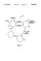
- FIG. 7is a diagram of an algorithmic state machine 700 embodied within slave device 600. Upon reset of the system, state machine 700 enters state 710 during which line 127 is tri-stated by slave 600. State machine 700 remains in state 710 for as long as the clock request signal CLKREQ at line 127 is low.
- state machine 700When the clock request signal CLKREQ at line 127 goes high, state machine 700 enters state 720. During state 720, line 127 continues to be tri-stated by slave device 600. State machine 700 remains in state 720 for as long as the clock request signal CLKREQ remains high and while there is no need for the peripheral bus clock signal CLK.
- state machine 700If the clock request signal CLKREQ at line 127 falls back low, state machine 700 returns to state 710. If, on the other hand, the peripheral bus clock signal CLK is needed by slave 600 and the clock request signal at line 127 is high, state machine 700 enters state 730. During state 730, the clock request signal at line 127 is pulled low by slave device 600 for two clock cycles. State machine 700 then re-enters state 710 and line 127 is tri-stated by slave device 600.
- FIG. 8is a diagram of an alternative embodiment of a state machine 800 embodied within the clock control circuit 120 of FIGS. 2, 4 and 6.
- State machine 800is responsive to clock request signals (i.e., CLKREQ) asserted by both master and slave devices.
- clock request signalsi.e., CLKREQ
- both the re-starting and the stopping of the peripheral bus clock signalare directly controlled by clock control circuit 120.
- power management unit 111may be configured to control clock generator 122 at other times during the operation of the computer system.
- state machine 800Upon reset, state machine 800 enters state 810 during which the clock request signal CLKREQ at line 127 is tri-stated and is passively pulled high by the clock control circuit 120 and during which the peripheral bus clock signal CLK is on. If the clock request signal at line 127 is detected high for a predetermined number of clocks (i.e., M clock cycles), state machine 800 enters state 820.
- line 127continues to be tri-stated and pulled high by the clock control circuit 120 and the peripheral bus clock signal CLK is stopped. It is noted that clock generator 122 is directly controlled through power management unit 111 by clock control circuit 120 to stop the peripheral bus clock signal CLK.
- the state machine 800remains in state 820 until the clock request signal CLKREQ at line 127 is pulled low, for example, by alternate bus master 108. When the clock request signal CLKREQ is asserted low, state machine 800 reverts back to state 810 and the peripheral bus clock signal CLK is re-started.
- state machine 800On the next clock cycle, state machine 800 will enter state 830 if the clock request signal CLKREQ continues to be asserted low. During state 830, the clock control circuit 120 maintains the low drive at line 127 so the master or slave device can release the drive. If a synchronous bus request signal (i.e., SREQx) is asserted, state machine 800 remains in state 830 until the bus request signal is deasserted high. If no bus request signal SREQx is asserted low and a predetermined number of clock cycles (i.e., N clocks) have transpired, state machine 800 enters state 840. During state 840, the clock request signal CLKREQ at line 127 is asserted high for one clock cycle by clock control circuit 120. State machine 800 then reverts back to state 810.
- SREQxsynchronous bus request signal
- State machine 800will remain in state 810 until the clock request signal at line 127 is again pulled low, thereby causing state machine 800 to enter state 830, or until M clock cycles have transpired, at which state machine 800 will enter state 820 and the peripheral bus clock signal will be stopped.
- slave device 600if slave device 600 requires that the peripheral clock signal CLK remain on, it will detect the low assertion of the clock request signal (referred to generally as an "indicator" signal) at line 127 by the clock control circuit 120 (i.e., during state 340, FIG. 3 or state 840, FIG. 8) and will drive the clock request signal low to keep the clock running for an additional timed period as determined by state 330 for the state machine 300 (of FIG. 3) or by state 830 for the state machine 800 (of FIG. 8).
- an indicator signalreferred to generally as an "indicator” signal
- the algorithmic state machines 300, 500, 700 and 800may be reduced to sequential logic circuits by employing a variety of well known circuit reduction techniques.
- sequential logic circuitry that implements state machines 300 and 500may be attained in accordance with the state reduction techniques taught within the publication Digital Design by M. Morris Mano, Prentice-Hall, Inc., pp 220-236; and within the publication Digital Computer Fundamentals--6th Edition by Thomas Bartee, McGraw-Hill Book Company, pp 170-175. These publications are incorporated herein by reference.
- Computer-aided design toolsmay alteratively be employed to reduce the state machines 300, 500, 700 and 800 to sequential logic circuits.
- Exemplary computer-aided design toolsinclude the VHSIC hardware description language and the VERILOG description language.
- the power management unit 111 of FIGS. 2 and 4may be configured to implement a variety of additional power management functions in addition to that described above.
- power management unit 111may be designed to implement functions similar to those described in U.S. Pat. No. 5,167,024 issued Nov. 24, 1992 to Smith et al. This patent is incorporated herein by reference in its entirety.
- slave device 600could be embodied by a variety of specific peripheral devices.
- slave device 600could be a disk controller device or an audio controller device.
- clock generator of 122is shown within a bus interface and arbiter unit 106 in the embodiments described above, the clock generator 122 could be incorporated within a variety of alternative circuit blocks of computer system 100.
Landscapes
- Engineering & Computer Science (AREA)
- Theoretical Computer Science (AREA)
- Physics & Mathematics (AREA)
- General Engineering & Computer Science (AREA)
- General Physics & Mathematics (AREA)
- Information Transfer Systems (AREA)
- Power Sources (AREA)
Abstract
Description
Claims (18)
Priority Applications (5)
| Application Number | Priority Date | Filing Date | Title |
|---|---|---|---|
| US08/131,092US5600839A (en) | 1993-10-01 | 1993-10-01 | System and method for controlling assertion of a peripheral bus clock signal through a slave device |
| EP94306661AEP0644475B1 (en) | 1993-09-22 | 1994-09-12 | Apparatus and method for controlling a peripheral bus clock signal |
| DE69433906TDE69433906T2 (en) | 1993-09-22 | 1994-09-12 | Apparatus and method for controlling a peripheral bus clock signal |
| JP22433694AJP3568592B2 (en) | 1993-09-22 | 1994-09-20 | Computer system and method for controlling peripheral bus clock signals |
| JP23474794AJP3526920B2 (en) | 1993-10-01 | 1994-09-29 | Computer system and system and method for controlling peripheral bus clock signals |
Applications Claiming Priority (1)
| Application Number | Priority Date | Filing Date | Title |
|---|---|---|---|
| US08/131,092US5600839A (en) | 1993-10-01 | 1993-10-01 | System and method for controlling assertion of a peripheral bus clock signal through a slave device |
Publications (1)
| Publication Number | Publication Date |
|---|---|
| US5600839Atrue US5600839A (en) | 1997-02-04 |
Family
ID=22447844
Family Applications (1)
| Application Number | Title | Priority Date | Filing Date |
|---|---|---|---|
| US08/131,092Expired - LifetimeUS5600839A (en) | 1993-09-22 | 1993-10-01 | System and method for controlling assertion of a peripheral bus clock signal through a slave device |
Country Status (2)
| Country | Link |
|---|---|
| US (1) | US5600839A (en) |
| JP (1) | JP3526920B2 (en) |
Cited By (52)
| Publication number | Priority date | Publication date | Assignee | Title |
|---|---|---|---|---|
| US6175929B1 (en)* | 1998-06-16 | 2001-01-16 | Asus Tek Computer Inc. | System clock switch circuit of a computer main board |
| US20020019953A1 (en)* | 2000-08-01 | 2002-02-14 | Fujitsu Limited, Kawasaki, Japan | Clock supply control apparatus and method |
| US20020056118A1 (en)* | 1999-08-27 | 2002-05-09 | Hunter Charles Eric | Video and music distribution system |
| US6397338B2 (en)* | 1995-05-26 | 2002-05-28 | National Semiconductor Corporation | Power management circuit that qualifies powergood disposal signal |
| US20020112235A1 (en)* | 2001-02-12 | 2002-08-15 | Ballou Bernard L. | Video distribution system |
| US20020111912A1 (en)* | 1999-08-27 | 2002-08-15 | Hunter Charles Eric | Music distribution systems |
| US20020112243A1 (en)* | 2001-02-12 | 2002-08-15 | World Theatre | Video distribution system |
| US20020126616A1 (en)* | 2000-10-20 | 2002-09-12 | Hunter Charles Eric | High capacity digital data storage by transmission of radiant energy through arrays of small diameter holes |
| US20020156858A1 (en)* | 1999-04-28 | 2002-10-24 | Hunter Charles Eric | System permitting retail stores to place advertisements on roadside electronic billboard displays that tie into point of purchase displays at the stores |
| US20020165776A1 (en)* | 1999-04-28 | 2002-11-07 | Hunter Charles Eric | System for direct placement of commercial advertising, public service announcements and other content on electronic billboard displays |
| US20020183861A1 (en)* | 2001-05-04 | 2002-12-05 | Mcree Duncan | Determining structures by performing comparisons between molecular replacement results for multiple different biomolecules |
| US20030004806A1 (en)* | 2001-06-29 | 2003-01-02 | Vaitekunas Jeffrey J. | Business method of auctioning advertising |
| US20030004805A1 (en)* | 2001-06-29 | 2003-01-02 | Vaitekunas Jeffrey J. | Business method for billboard advertising |
| US20030001830A1 (en)* | 2001-06-29 | 2003-01-02 | Wampler Scott D. | Dynamic device for billboard advertising |
| US20030001796A1 (en)* | 2001-06-29 | 2003-01-02 | Wampler James W. | Advertising method for dynamic billboards |
| US20030037274A1 (en)* | 2001-08-15 | 2003-02-20 | Fujitsu Limited | Semiconductor device with hardware mechanism for proper clock control |
| US20030069002A1 (en)* | 2001-10-10 | 2003-04-10 | Hunter Charles Eric | System and method for emergency notification content delivery |
| US20030149989A1 (en)* | 2001-09-14 | 2003-08-07 | Hunter Charles Eric | Broadcast distribution of content for storage on hardware protected optical storage media |
| US20030159080A1 (en)* | 2002-02-19 | 2003-08-21 | Nec Electronics Corporation | Information processing unit |
| US6647417B1 (en) | 2000-02-10 | 2003-11-11 | World Theatre, Inc. | Music distribution systems |
| US20030234777A1 (en)* | 2002-06-19 | 2003-12-25 | Wampler Scott D. | Dynamic device and method for dispensing machines |
| US20040003297A1 (en)* | 2002-06-26 | 2004-01-01 | Kenneth Ma | Method and apparatus for the conditional enablement of PCI power management |
| US6763478B1 (en)* | 2000-10-24 | 2004-07-13 | Dell Products, L.P. | Variable clock cycle for processor, bus and components for power management in an information handling system |
| US6850901B1 (en) | 1999-12-17 | 2005-02-01 | World Theatre, Inc. | System and method permitting customers to order products from multiple participating merchants |
| US20050182730A1 (en)* | 1999-08-27 | 2005-08-18 | Ochoa Optics, Llc | Music distribution system and associated antipiracy protection |
| US20050198429A1 (en)* | 2004-03-02 | 2005-09-08 | Nec Electronics Corporation | Multilayer system and clock control method |
| US20050198418A1 (en)* | 2004-03-02 | 2005-09-08 | Nec Electronics Corporation | Multilayer system and clock control method |
| US20060026330A1 (en)* | 2004-07-28 | 2006-02-02 | Yi Doo-Youll | Bus arbitration system that achieves power savings based on selective clock control |
| US20060111981A1 (en)* | 1999-04-28 | 2006-05-25 | Hunter Charles E | Methods and apparatus for ultra-violet stimulated displays |
| US20060195548A1 (en)* | 1999-08-27 | 2006-08-31 | Ochoa Optics Llc | Video distribution system |
| US20060212908A1 (en)* | 1999-08-27 | 2006-09-21 | Ochoa Optics Llc | Video distribution system |
| US20060293971A1 (en)* | 1999-12-17 | 2006-12-28 | Ochoa Optics Llc | System and Method Permitting Customers to Order Selected Products from a Vast Array of Products Offered By Multiple Participating Merchants and Related Security Publications |
| US20070067652A1 (en)* | 2005-08-22 | 2007-03-22 | Oki Electric Industry Co., Ltd. | System using bus arbiter to power down |
| US7245631B2 (en) | 2001-04-27 | 2007-07-17 | Mitsubishi Jidosha Kogyo Kabushiki Kaisha | Multiplex communication apparatus for vehicle |
| US20070276740A1 (en)* | 1999-08-27 | 2007-11-29 | Ochoa Optics, Llc | Music distribution systems |
| US7370016B1 (en) | 1999-08-27 | 2008-05-06 | Ochoa Optics Llc | Music distribution systems |
| US20090031060A1 (en)* | 2007-07-24 | 2009-01-29 | Masaharu Adachi | Bus converter, semiconductor device, and noise reduction method of bus converter and semiconductor device |
| US20090158076A1 (en)* | 2007-12-13 | 2009-06-18 | Umesh Chandra Chejara | Technique to implement clock-gating |
| US7596708B1 (en) | 2000-01-18 | 2009-09-29 | Sameer Halepete | Adaptive power control |
| US20100146169A1 (en)* | 2008-12-05 | 2010-06-10 | Nuvoton Technology Corporation | Bus-handling |
| US7895088B2 (en) | 1999-04-28 | 2011-02-22 | Novus Partners, Llc | System permitting the display of video or still image content on selected displays of an electronic display network according to customer dictates |
| US8112311B2 (en) | 2001-02-12 | 2012-02-07 | Ochoa Optics Llc | Systems and methods for distribution of entertainment and advertising content |
| US8966302B2 (en)* | 2010-06-23 | 2015-02-24 | Broadcom Corporation | Method for power management of data buses in electronic devices |
| US9252898B2 (en) | 2000-01-28 | 2016-02-02 | Zarbaña Digital Fund Llc | Music distribution systems |
| US9305590B2 (en) | 2007-10-16 | 2016-04-05 | Seagate Technology Llc | Prevent data storage device circuitry swap |
| US9679602B2 (en) | 2006-06-14 | 2017-06-13 | Seagate Technology Llc | Disc drive circuitry swap |
| US10248155B2 (en) | 2016-01-25 | 2019-04-02 | Samsung Electronics Co., Ltd. | Semiconductor device including clock generating circuit and channel management circuit |
| US10296066B2 (en) | 2016-01-25 | 2019-05-21 | Samsung Electronics Co., Ltd. | Semiconductor device, semiconductor system, and method of operating the semiconductor device |
| US10303203B2 (en) | 2016-01-25 | 2019-05-28 | Samsung Electronics Co., Ltd. | Semiconductor device, semiconductor system and method for operating semiconductor device |
| US10311191B2 (en) | 2017-01-26 | 2019-06-04 | Advanced Micro Devices, Inc. | Memory including side-car arrays with irregular sized entries |
| US10969854B2 (en) | 2016-01-25 | 2021-04-06 | Samsung Electronics Co., Ltd. | Semiconductor device including clock management unit for outputing clock and acknowledgement signals to an intellectual property block |
| US11314278B2 (en) | 2016-01-25 | 2022-04-26 | Samsung Electronics Co., Ltd. | Semiconductor device, semiconductor system and method for operating semiconductor device |
Families Citing this family (1)
| Publication number | Priority date | Publication date | Assignee | Title |
|---|---|---|---|---|
| JP2760958B2 (en)* | 1995-06-14 | 1998-06-04 | ユナイテッド マイクロエレクトロニクス コーポレイション | Computer device and power management method thereof |
Citations (18)
| Publication number | Priority date | Publication date | Assignee | Title |
|---|---|---|---|---|
| US4545030A (en)* | 1982-09-28 | 1985-10-01 | The John Hopkins University | Synchronous clock stopper for microprocessor |
| US4835737A (en)* | 1986-07-21 | 1989-05-30 | American Telephone And Telegraph Company, At&T Bell Laboratories | Method and apparatus for controlled removal and insertion of circuit modules |
| US5021950A (en)* | 1984-12-27 | 1991-06-04 | Kabushiki Kaisha Toshiba | Multiprocessor system with standby function |
| US5150467A (en)* | 1987-09-04 | 1992-09-22 | Digital Equipment Corporation | Method and apparatus for suspending and restarting a bus cycle |
| US5167024A (en)* | 1989-09-08 | 1992-11-24 | Apple Computer, Inc. | Power management for a laptop computer with slow and sleep modes |
| US5189647A (en)* | 1991-02-25 | 1993-02-23 | International Business Machines Corp. | Information processing system having power saving control of the processor clock |
| US5195185A (en)* | 1990-09-21 | 1993-03-16 | International Business Machines Corporation | Dynamic bus arbitration with concurrent same bus granting every cycle |
| US5202966A (en)* | 1991-09-06 | 1993-04-13 | Rockwell International Corporation | Centralized bus arbitration circuit |
| US5237692A (en)* | 1990-11-09 | 1993-08-17 | Ast Research Inc. | Internal interrupt controller for a peripheral controller |
| US5339445A (en)* | 1992-11-16 | 1994-08-16 | Harris Corporation | Method of autonomously reducing power consumption in a computer sytem by compiling a history of power consumption |
| US5363492A (en)* | 1990-08-31 | 1994-11-08 | Ncr Corporation | Internal bus for work station interfacing means |
| US5390350A (en)* | 1991-04-22 | 1995-02-14 | Western Digital Corporation | Integrated circuit chip core logic system controller with power saving features for a microcomputer system |
| US5404546A (en)* | 1991-02-14 | 1995-04-04 | Dell Usa | BIOS independent power management for portable computer |
| US5428790A (en)* | 1989-06-30 | 1995-06-27 | Fujitsu Personal Systems, Inc. | Computer power management system |
| US5450574A (en)* | 1993-03-29 | 1995-09-12 | All Computers Inc. | Apparatus and method for enhancing the performance of personal computers |
| US5452434A (en)* | 1992-07-14 | 1995-09-19 | Advanced Micro Devices, Inc. | Clock control for power savings in high performance central processing units |
| US5461652A (en)* | 1994-04-06 | 1995-10-24 | Mitsubishi Denki Kabushiki Kaisha | Clock control circuit |
| US5493684A (en)* | 1994-04-06 | 1996-02-20 | Advanced Micro Devices | Power management architecture including a power management messaging bus for conveying an encoded activity signal for optimal flexibility |
- 1993
- 1993-10-01USUS08/131,092patent/US5600839A/ennot_activeExpired - Lifetime
- 1994
- 1994-09-29JPJP23474794Apatent/JP3526920B2/ennot_activeExpired - Fee Related
Patent Citations (18)
| Publication number | Priority date | Publication date | Assignee | Title |
|---|---|---|---|---|
| US4545030A (en)* | 1982-09-28 | 1985-10-01 | The John Hopkins University | Synchronous clock stopper for microprocessor |
| US5021950A (en)* | 1984-12-27 | 1991-06-04 | Kabushiki Kaisha Toshiba | Multiprocessor system with standby function |
| US4835737A (en)* | 1986-07-21 | 1989-05-30 | American Telephone And Telegraph Company, At&T Bell Laboratories | Method and apparatus for controlled removal and insertion of circuit modules |
| US5150467A (en)* | 1987-09-04 | 1992-09-22 | Digital Equipment Corporation | Method and apparatus for suspending and restarting a bus cycle |
| US5428790A (en)* | 1989-06-30 | 1995-06-27 | Fujitsu Personal Systems, Inc. | Computer power management system |
| US5167024A (en)* | 1989-09-08 | 1992-11-24 | Apple Computer, Inc. | Power management for a laptop computer with slow and sleep modes |
| US5363492A (en)* | 1990-08-31 | 1994-11-08 | Ncr Corporation | Internal bus for work station interfacing means |
| US5195185A (en)* | 1990-09-21 | 1993-03-16 | International Business Machines Corporation | Dynamic bus arbitration with concurrent same bus granting every cycle |
| US5237692A (en)* | 1990-11-09 | 1993-08-17 | Ast Research Inc. | Internal interrupt controller for a peripheral controller |
| US5404546A (en)* | 1991-02-14 | 1995-04-04 | Dell Usa | BIOS independent power management for portable computer |
| US5189647A (en)* | 1991-02-25 | 1993-02-23 | International Business Machines Corp. | Information processing system having power saving control of the processor clock |
| US5390350A (en)* | 1991-04-22 | 1995-02-14 | Western Digital Corporation | Integrated circuit chip core logic system controller with power saving features for a microcomputer system |
| US5202966A (en)* | 1991-09-06 | 1993-04-13 | Rockwell International Corporation | Centralized bus arbitration circuit |
| US5452434A (en)* | 1992-07-14 | 1995-09-19 | Advanced Micro Devices, Inc. | Clock control for power savings in high performance central processing units |
| US5339445A (en)* | 1992-11-16 | 1994-08-16 | Harris Corporation | Method of autonomously reducing power consumption in a computer sytem by compiling a history of power consumption |
| US5450574A (en)* | 1993-03-29 | 1995-09-12 | All Computers Inc. | Apparatus and method for enhancing the performance of personal computers |
| US5461652A (en)* | 1994-04-06 | 1995-10-24 | Mitsubishi Denki Kabushiki Kaisha | Clock control circuit |
| US5493684A (en)* | 1994-04-06 | 1996-02-20 | Advanced Micro Devices | Power management architecture including a power management messaging bus for conveying an encoded activity signal for optimal flexibility |
Cited By (104)
| Publication number | Priority date | Publication date | Assignee | Title |
|---|---|---|---|---|
| US6397338B2 (en)* | 1995-05-26 | 2002-05-28 | National Semiconductor Corporation | Power management circuit that qualifies powergood disposal signal |
| US6175929B1 (en)* | 1998-06-16 | 2001-01-16 | Asus Tek Computer Inc. | System clock switch circuit of a computer main board |
| US20020156858A1 (en)* | 1999-04-28 | 2002-10-24 | Hunter Charles Eric | System permitting retail stores to place advertisements on roadside electronic billboard displays that tie into point of purchase displays at the stores |
| US20060111981A1 (en)* | 1999-04-28 | 2006-05-25 | Hunter Charles E | Methods and apparatus for ultra-violet stimulated displays |
| US20050273390A1 (en)* | 1999-04-28 | 2005-12-08 | Hunter Charles E | System for placement of content on electronic billboard displays |
| US7895088B2 (en) | 1999-04-28 | 2011-02-22 | Novus Partners, Llc | System permitting the display of video or still image content on selected displays of an electronic display network according to customer dictates |
| US20020165776A1 (en)* | 1999-04-28 | 2002-11-07 | Hunter Charles Eric | System for direct placement of commercial advertising, public service announcements and other content on electronic billboard displays |
| US8656423B2 (en) | 1999-08-27 | 2014-02-18 | Ochoa Optics Llc | Video distribution system |
| US20020111912A1 (en)* | 1999-08-27 | 2002-08-15 | Hunter Charles Eric | Music distribution systems |
| US20060195548A1 (en)* | 1999-08-27 | 2006-08-31 | Ochoa Optics Llc | Video distribution system |
| US20060294016A1 (en)* | 1999-08-27 | 2006-12-28 | Ochoa Optics Llc | Music distribution system and associated antipiracy protections |
| US6952685B1 (en) | 1999-08-27 | 2005-10-04 | Ochoa Optics Llc | Music distribution system and associated antipiracy protection |
| US8090619B1 (en) | 1999-08-27 | 2012-01-03 | Ochoa Optics Llc | Method and system for music distribution |
| US8019688B2 (en) | 1999-08-27 | 2011-09-13 | Ochoa Optics Llc | Music distribution system and associated antipiracy protections |
| US8719878B2 (en) | 1999-08-27 | 2014-05-06 | Ochoa Optics Llc | Video distribution system |
| US20060212908A1 (en)* | 1999-08-27 | 2006-09-21 | Ochoa Optics Llc | Video distribution system |
| US20050182730A1 (en)* | 1999-08-27 | 2005-08-18 | Ochoa Optics, Llc | Music distribution system and associated antipiracy protection |
| US7647618B1 (en) | 1999-08-27 | 2010-01-12 | Charles Eric Hunter | Video distribution system |
| US20020056118A1 (en)* | 1999-08-27 | 2002-05-09 | Hunter Charles Eric | Video and music distribution system |
| US7370016B1 (en) | 1999-08-27 | 2008-05-06 | Ochoa Optics Llc | Music distribution systems |
| US9659285B2 (en) | 1999-08-27 | 2017-05-23 | Zarbaña Digital Fund Llc | Music distribution systems |
| US20070276740A1 (en)* | 1999-08-27 | 2007-11-29 | Ochoa Optics, Llc | Music distribution systems |
| US7209900B2 (en) | 1999-08-27 | 2007-04-24 | Charles Eric Hunter | Music distribution systems |
| US6850901B1 (en) | 1999-12-17 | 2005-02-01 | World Theatre, Inc. | System and method permitting customers to order products from multiple participating merchants |
| US20060293971A1 (en)* | 1999-12-17 | 2006-12-28 | Ochoa Optics Llc | System and Method Permitting Customers to Order Selected Products from a Vast Array of Products Offered By Multiple Participating Merchants and Related Security Publications |
| US7596708B1 (en) | 2000-01-18 | 2009-09-29 | Sameer Halepete | Adaptive power control |
| US20100011233A1 (en)* | 2000-01-18 | 2010-01-14 | Sameer Halepete | Adaptive power control |
| US8566627B2 (en) | 2000-01-18 | 2013-10-22 | Sameer Halepete | Adaptive power control |
| US8806247B2 (en) | 2000-01-18 | 2014-08-12 | Intellectual Venture Funding Llc | Adaptive power control |
| US9252898B2 (en) | 2000-01-28 | 2016-02-02 | Zarbaña Digital Fund Llc | Music distribution systems |
| US6647417B1 (en) | 2000-02-10 | 2003-11-11 | World Theatre, Inc. | Music distribution systems |
| USRE41137E1 (en) | 2000-02-10 | 2010-02-16 | Charles Eric Hunter | Music distribution systems |
| US6931563B2 (en)* | 2000-08-01 | 2005-08-16 | Fujitsu Limited | Clock supply controller supplies an independent clock control signal to a PCMCIA controller which generates an interrupt signal |
| US20020019953A1 (en)* | 2000-08-01 | 2002-02-14 | Fujitsu Limited, Kawasaki, Japan | Clock supply control apparatus and method |
| US7649827B2 (en) | 2000-10-20 | 2010-01-19 | Charles Eric Hunter | High capacity digital data storage by transmission of radiant energy through arrays of small diameter holes |
| US7054256B2 (en) | 2000-10-20 | 2006-05-30 | Ochoa Optics Llc | High capacity digital data storage by transmission of radiant energy through arrays of small diameter holes |
| US20060164962A1 (en)* | 2000-10-20 | 2006-07-27 | Ochoa Optics Llc | High capacity digital data storage by transmission of radiant energy through arrays of small diameter holes |
| US20060164958A1 (en)* | 2000-10-20 | 2006-07-27 | Ochoa Optics Llc | High capacity digital data storage by transmission of radiant energy through arrays of small diameter holes |
| US20100080110A1 (en)* | 2000-10-20 | 2010-04-01 | Charles Eric Hunter | High Capacity Digital Data Storage By Transmission of Radiant Energy Through Arrays of Small Diameter Holes |
| US7623436B2 (en) | 2000-10-20 | 2009-11-24 | Charles Eric Hunter | High capacity digital data storage by transmission of radiant energy through arrays of small diameter holes |
| US20020126616A1 (en)* | 2000-10-20 | 2002-09-12 | Hunter Charles Eric | High capacity digital data storage by transmission of radiant energy through arrays of small diameter holes |
| US6763478B1 (en)* | 2000-10-24 | 2004-07-13 | Dell Products, L.P. | Variable clock cycle for processor, bus and components for power management in an information handling system |
| US20020112235A1 (en)* | 2001-02-12 | 2002-08-15 | Ballou Bernard L. | Video distribution system |
| US8112311B2 (en) | 2001-02-12 | 2012-02-07 | Ochoa Optics Llc | Systems and methods for distribution of entertainment and advertising content |
| US20020112243A1 (en)* | 2001-02-12 | 2002-08-15 | World Theatre | Video distribution system |
| DE10292207B4 (en)* | 2001-04-27 | 2007-10-25 | Mitsubishi Jidosha Kogyo K.K. | Vehicle multiplex communication system |
| US7245631B2 (en) | 2001-04-27 | 2007-07-17 | Mitsubishi Jidosha Kogyo Kabushiki Kaisha | Multiplex communication apparatus for vehicle |
| US20020183861A1 (en)* | 2001-05-04 | 2002-12-05 | Mcree Duncan | Determining structures by performing comparisons between molecular replacement results for multiple different biomolecules |
| US20030004806A1 (en)* | 2001-06-29 | 2003-01-02 | Vaitekunas Jeffrey J. | Business method of auctioning advertising |
| US20030001830A1 (en)* | 2001-06-29 | 2003-01-02 | Wampler Scott D. | Dynamic device for billboard advertising |
| US20060290592A1 (en)* | 2001-06-29 | 2006-12-28 | Wampler James W | Advertising method for dynamic billboards |
| US7015875B2 (en) | 2001-06-29 | 2006-03-21 | Novus Partners Llc | Dynamic device for billboard advertising |
| US20030001796A1 (en)* | 2001-06-29 | 2003-01-02 | Wampler James W. | Advertising method for dynamic billboards |
| US20030004805A1 (en)* | 2001-06-29 | 2003-01-02 | Vaitekunas Jeffrey J. | Business method for billboard advertising |
| US7098869B2 (en) | 2001-06-29 | 2006-08-29 | Novus Partners Llc | Business method for billboard advertising |
| US7098870B2 (en) | 2001-06-29 | 2006-08-29 | Novus Partners Llc | Advertising method for dynamic billboards |
| US7093152B2 (en) | 2001-08-15 | 2006-08-15 | Fujitsu Limited | Semiconductor device with a hardware mechanism for proper clock control |
| EP1286248A3 (en)* | 2001-08-15 | 2003-08-27 | Fujitsu Limited | Semiconductor device with hardware mechanism for proper clock control |
| US20030037274A1 (en)* | 2001-08-15 | 2003-02-20 | Fujitsu Limited | Semiconductor device with hardware mechanism for proper clock control |
| US7960005B2 (en) | 2001-09-14 | 2011-06-14 | Ochoa Optics Llc | Broadcast distribution of content for storage on hardware protected optical storage media |
| US20030149989A1 (en)* | 2001-09-14 | 2003-08-07 | Hunter Charles Eric | Broadcast distribution of content for storage on hardware protected optical storage media |
| US9514632B2 (en) | 2001-10-10 | 2016-12-06 | Google Inc. | Dangerous condition detection with user feedback |
| US9847008B2 (en) | 2001-10-10 | 2017-12-19 | Google Inc. | Remote sensors for detecting alert conditions and notifying a central station |
| US20030069002A1 (en)* | 2001-10-10 | 2003-04-10 | Hunter Charles Eric | System and method for emergency notification content delivery |
| US9147338B2 (en) | 2001-10-10 | 2015-09-29 | Google Inc. | System and method for emergency notification content delivery |
| US10540878B2 (en) | 2001-10-10 | 2020-01-21 | Google Llc | Remote sensors for detecting alert conditions and notifying a central station |
| US20070275690A1 (en)* | 2001-10-10 | 2007-11-29 | Ochoa Optics Llc | System and Method for Emergency Notification Content Delivery |
| US8412147B2 (en) | 2001-10-10 | 2013-04-02 | Ochoa Optics Llc | System and method for emergency notification content delivery |
| US7233781B2 (en) | 2001-10-10 | 2007-06-19 | Ochoa Optics Llc | System and method for emergency notification content delivery |
| US10062260B2 (en) | 2001-10-10 | 2018-08-28 | Google Llc | Remote sensors for detecting alert conditions and notifying a central station |
| US9613521B2 (en) | 2001-10-10 | 2017-04-04 | Google Inc. | Remote sensors for detecting alert conditions and notifying a central station |
| US7155631B2 (en)* | 2002-02-19 | 2006-12-26 | Nec Electronics Corporation | Information processing unit with a clock control circuit having access to the system bus during system clock changes |
| US20030159080A1 (en)* | 2002-02-19 | 2003-08-21 | Nec Electronics Corporation | Information processing unit |
| EP1345109A3 (en)* | 2002-02-19 | 2006-02-22 | NEC Electronics Corporation | Information processing unit |
| US7088352B2 (en) | 2002-06-19 | 2006-08-08 | Novus Partners Llc | Dynamic device and method for dispensing machines |
| US20030234777A1 (en)* | 2002-06-19 | 2003-12-25 | Wampler Scott D. | Dynamic device and method for dispensing machines |
| US20040003297A1 (en)* | 2002-06-26 | 2004-01-01 | Kenneth Ma | Method and apparatus for the conditional enablement of PCI power management |
| US6959395B2 (en)* | 2002-06-26 | 2005-10-25 | Broadcom Corporation | Method and apparatus for the conditional enablement of PCI power management |
| US20050198418A1 (en)* | 2004-03-02 | 2005-09-08 | Nec Electronics Corporation | Multilayer system and clock control method |
| US20050198429A1 (en)* | 2004-03-02 | 2005-09-08 | Nec Electronics Corporation | Multilayer system and clock control method |
| US7277976B2 (en)* | 2004-03-02 | 2007-10-02 | Nec Electronics Corporation | Multilayer system and clock control method |
| US20060026330A1 (en)* | 2004-07-28 | 2006-02-02 | Yi Doo-Youll | Bus arbitration system that achieves power savings based on selective clock control |
| US20070067652A1 (en)* | 2005-08-22 | 2007-03-22 | Oki Electric Industry Co., Ltd. | System using bus arbiter to power down |
| US9679602B2 (en) | 2006-06-14 | 2017-06-13 | Seagate Technology Llc | Disc drive circuitry swap |
| US8010730B2 (en)* | 2007-07-24 | 2011-08-30 | Ricoh Company, Ltd. | Bus converter, semiconductor device, and noise reduction method of bus converter and semiconductor device |
| US20090031060A1 (en)* | 2007-07-24 | 2009-01-29 | Masaharu Adachi | Bus converter, semiconductor device, and noise reduction method of bus converter and semiconductor device |
| US9305590B2 (en) | 2007-10-16 | 2016-04-05 | Seagate Technology Llc | Prevent data storage device circuitry swap |
| US20090158076A1 (en)* | 2007-12-13 | 2009-06-18 | Umesh Chandra Chejara | Technique to implement clock-gating |
| US7861192B2 (en) | 2007-12-13 | 2010-12-28 | Globalfoundries Inc. | Technique to implement clock-gating using a common enable for a plurality of storage cells |
| US20120166826A1 (en)* | 2008-12-05 | 2012-06-28 | Nuvoton Technology Corporation | Bus-handling |
| US20100146169A1 (en)* | 2008-12-05 | 2010-06-10 | Nuvoton Technology Corporation | Bus-handling |
| US8307233B2 (en)* | 2008-12-05 | 2012-11-06 | Nuvoton Technology Corporation | Bus-handling |
| US8966302B2 (en)* | 2010-06-23 | 2015-02-24 | Broadcom Corporation | Method for power management of data buses in electronic devices |
| US11314278B2 (en) | 2016-01-25 | 2022-04-26 | Samsung Electronics Co., Ltd. | Semiconductor device, semiconductor system and method for operating semiconductor device |
| US10296065B2 (en) | 2016-01-25 | 2019-05-21 | Samsung Electronics Co., Ltd. | Clock management using full handshaking |
| US10303203B2 (en) | 2016-01-25 | 2019-05-28 | Samsung Electronics Co., Ltd. | Semiconductor device, semiconductor system and method for operating semiconductor device |
| US10296066B2 (en) | 2016-01-25 | 2019-05-21 | Samsung Electronics Co., Ltd. | Semiconductor device, semiconductor system, and method of operating the semiconductor device |
| US10928849B2 (en) | 2016-01-25 | 2021-02-23 | Samsung Electronics Co., Ltd. | Semiconductor device, semiconductor system and method for operating semiconductor device |
| US10969854B2 (en) | 2016-01-25 | 2021-04-06 | Samsung Electronics Co., Ltd. | Semiconductor device including clock management unit for outputing clock and acknowledgement signals to an intellectual property block |
| US10248155B2 (en) | 2016-01-25 | 2019-04-02 | Samsung Electronics Co., Ltd. | Semiconductor device including clock generating circuit and channel management circuit |
| US11340685B2 (en) | 2016-01-25 | 2022-05-24 | Samsung Electronics Co., Ltd. | Semiconductor device including clock management unit for outputting clock and acknowledgment signals to an intelectual property block |
| US11747853B2 (en) | 2016-01-25 | 2023-09-05 | Samsung Electronics Co., Ltd. | Semiconductor device, semiconductor system and method for operating semiconductor device |
| US11789515B2 (en) | 2016-01-25 | 2023-10-17 | Samsung Electronics Co., Ltd. | Semiconductor device |
| US10311191B2 (en) | 2017-01-26 | 2019-06-04 | Advanced Micro Devices, Inc. | Memory including side-car arrays with irregular sized entries |
Also Published As
| Publication number | Publication date |
|---|---|
| JPH07152450A (en) | 1995-06-16 |
| JP3526920B2 (en) | 2004-05-17 |
Similar Documents
| Publication | Publication Date | Title |
|---|---|---|
| US5600839A (en) | System and method for controlling assertion of a peripheral bus clock signal through a slave device | |
| US5628019A (en) | System and method for controlling a peripheral bus clock signal during a reduced power mode | |
| US6163848A (en) | System and method for re-starting a peripheral bus clock signal and requesting mastership of a peripheral bus | |
| US5625807A (en) | System and method for enabling and disabling a clock run function to control a peripheral bus clock signal | |
| US7188262B2 (en) | Bus arbitration in low power system | |
| US7155618B2 (en) | Low power system and method for a data processing system | |
| US5590341A (en) | Method and apparatus for reducing power consumption in a computer system using ready delay | |
| US6115823A (en) | System and method for task performance based dynamic distributed power management in a computer system and design method therefor | |
| US6151651A (en) | Communication link with isochronous and asynchronous priority modes coupling bridge circuits in a computer system | |
| US6148357A (en) | Integrated CPU and memory controller utilizing a communication link having isochronous and asynchronous priority modes | |
| US7707340B2 (en) | Bus system and method of burst cycle conversion | |
| EP0820018A2 (en) | Circuit for handling distributed arbitration in a computer system having multiple arbiters | |
| US6611893B1 (en) | Data bus method and apparatus providing variable data rates using a smart bus arbiter | |
| US7155631B2 (en) | Information processing unit with a clock control circuit having access to the system bus during system clock changes | |
| EP0644475B1 (en) | Apparatus and method for controlling a peripheral bus clock signal | |
| US5524215A (en) | Bus protocol and method for controlling a data processor | |
| JP4182246B2 (en) | Bus sharing system and bus sharing method | |
| JPH10320349A (en) | Processor and data transfer system using the processor | |
| JPH10133766A (en) | Adaptive power-down clock control | |
| JP3713488B2 (en) | Computer system and operation control method thereof | |
| JPH11328111A (en) | Clock synchronous bus circuit |
Legal Events
| Date | Code | Title | Description |
|---|---|---|---|
| AS | Assignment | Owner name:ADVANCED MICRO DEVICES, INC., CALIFORNIA Free format text:ASSIGNMENT OF ASSIGNORS INTEREST;ASSIGNOR:MACDONALD, JAMES R.;REEL/FRAME:006720/0400 Effective date:19931001 | |
| STCF | Information on status: patent grant | Free format text:PATENTED CASE | |
| AS | Assignment | Owner name:IMPERIAL BANK, CALIFORNIA Free format text:COLLATERAL ASSIGNMENT, PATENT MORTGAGE AND SECURITY AGREEMENT;ASSIGNOR:REPLAY NETWORKS, INC.;REEL/FRAME:010043/0586 Effective date:19990610 | |
| FPAY | Fee payment | Year of fee payment:4 | |
| AS | Assignment | Owner name:IMPERIAL BANK, CALIFORNIA Free format text:AMENDMENT NO. 1 TO COLLATERAL ASSIGNMENT, PATENT MORTGAGE AND SECURITY AGREEMENT;ASSIGNOR:REPLAYTV, INC.;REEL/FRAME:011533/0767 Effective date:20000930 | |
| AS | Assignment | Owner name:REPLAYTV, INC., CALIFORNIA Free format text:CHANGE OF NAME;ASSIGNOR:REPLAY NETWORKS, INC.;REEL/FRAME:011506/0085 Effective date:20000118 | |
| AS | Assignment | Owner name:DIGITAL NETWORKS NORTH AMERICA, INC., CALIFORNIA Free format text:ASSET PURCHASE;ASSIGNOR:REPLAYTV, INC.;REEL/FRAME:014337/0499 Effective date:20030424 | |
| FEPP | Fee payment procedure | Free format text:PAYOR NUMBER ASSIGNED (ORIGINAL EVENT CODE: ASPN); ENTITY STATUS OF PATENT OWNER: LARGE ENTITY | |
| AS | Assignment | Owner name:DEUTSCHE BANK AG, TOKYO BRANCH, AS ADMINISTRATIVE AGENT, JAPAN Free format text:SECURITY AGREEMENT;ASSIGNOR:DIGITAL NETWORKS NORTH AMERICA, INC.;REEL/FRAME:014669/0612 Effective date:20040116 Owner name:DEUTSCHE BANK AG, TOKYO BRANCH, AS ADMINISTRATIVE Free format text:SECURITY AGREEMENT;ASSIGNOR:DIGITAL NETWORKS NORTH AMERICA, INC.;REEL/FRAME:014669/0612 Effective date:20040116 | |
| FPAY | Fee payment | Year of fee payment:8 | |
| AS | Assignment | Owner name:DIGITAL NETWORKS NORTH AMERICA, INC.,CALIFORNIA Free format text:RELEASE BY SECURED PARTY;ASSIGNOR:DEUTSCHE BANK AG, TOKYO BRANCH;REEL/FRAME:018375/0142 Effective date:20050125 Owner name:DIGITAL NETWORKS NORTH AMERICA, INC., CALIFORNIA Free format text:RELEASE BY SECURED PARTY;ASSIGNOR:DEUTSCHE BANK AG, TOKYO BRANCH;REEL/FRAME:018375/0142 Effective date:20050125 | |
| AS | Assignment | Owner name:REPLAYTV, INC., CALIFORNIA Free format text:RELEASE BY SECURED PARTY;ASSIGNOR:COMERICA BANK;REEL/FRAME:019690/0951 Effective date:20070723 | |
| FPAY | Fee payment | Year of fee payment:12 | |
| AS | Assignment | Owner name:GLOBALFOUNDRIES INC., CAYMAN ISLANDS Free format text:ASSIGNMENT OF ASSIGNORS INTEREST;ASSIGNOR:AMD TECHNOLOGIES HOLDINGS, INC.;REEL/FRAME:022764/0544 Effective date:20090302 Owner name:AMD TECHNOLOGIES HOLDINGS, INC., CALIFORNIA Free format text:ASSIGNMENT OF ASSIGNORS INTEREST;ASSIGNOR:ADVANCED MICRO DEVICES, INC.;REEL/FRAME:022764/0488 Effective date:20090302 | |
| AS | Assignment | Owner name:GLOBALFOUNDRIES U.S. INC., NEW YORK Free format text:RELEASE BY SECURED PARTY;ASSIGNOR:WILMINGTON TRUST, NATIONAL ASSOCIATION;REEL/FRAME:056987/0001 Effective date:20201117 |