US5598409A - Programmable telecommunications switch for personal computer - Google Patents
Programmable telecommunications switch for personal computerDownload PDFInfo
- Publication number
- US5598409A US5598409AUS08/651,123US65112396AUS5598409AUS 5598409 AUS5598409 AUS 5598409AUS 65112396 AUS65112396 AUS 65112396AUS 5598409 AUS5598409 AUS 5598409A
- Authority
- US
- United States
- Prior art keywords
- switch
- processor
- control
- host computer
- central call
- Prior art date
- Legal status (The legal status is an assumption and is not a legal conclusion. Google has not performed a legal analysis and makes no representation as to the accuracy of the status listed.)
- Expired - Lifetime
Links
Images


Classifications
- H—ELECTRICITY
- H04—ELECTRIC COMMUNICATION TECHNIQUE
- H04Q—SELECTING
- H04Q3/00—Selecting arrangements
- H04Q3/58—Arrangements providing connection between main exchange and sub-exchange or satellite
- H04Q3/62—Arrangements providing connection between main exchange and sub-exchange or satellite for connecting to private branch exchanges
- H04Q3/625—Arrangements in the private branch exchange
- H—ELECTRICITY
- H04—ELECTRIC COMMUNICATION TECHNIQUE
- H04Q—SELECTING
- H04Q11/00—Selecting arrangements for multiplex systems
- H04Q11/04—Selecting arrangements for multiplex systems for time-division multiplexing
- H04Q11/0407—Selecting arrangements for multiplex systems for time-division multiplexing using a stored programme control
- H04Q11/0414—Details
- H—ELECTRICITY
- H04—ELECTRIC COMMUNICATION TECHNIQUE
- H04Q—SELECTING
- H04Q2213/00—Indexing scheme relating to selecting arrangements in general and for multiplex systems
- H04Q2213/1305—Software aspects
- H—ELECTRICITY
- H04—ELECTRIC COMMUNICATION TECHNIQUE
- H04Q—SELECTING
- H04Q2213/00—Indexing scheme relating to selecting arrangements in general and for multiplex systems
- H04Q2213/1308—Power supply
- H—ELECTRICITY
- H04—ELECTRIC COMMUNICATION TECHNIQUE
- H04Q—SELECTING
- H04Q2213/00—Indexing scheme relating to selecting arrangements in general and for multiplex systems
- H04Q2213/13093—Personal computer, PC
- H—ELECTRICITY
- H04—ELECTRIC COMMUNICATION TECHNIQUE
- H04Q—SELECTING
- H04Q2213/00—Indexing scheme relating to selecting arrangements in general and for multiplex systems
- H04Q2213/13103—Memory
- H—ELECTRICITY
- H04—ELECTRIC COMMUNICATION TECHNIQUE
- H04Q—SELECTING
- H04Q2213/00—Indexing scheme relating to selecting arrangements in general and for multiplex systems
- H04Q2213/13106—Microprocessor, CPU
- H—ELECTRICITY
- H04—ELECTRIC COMMUNICATION TECHNIQUE
- H04Q—SELECTING
- H04Q2213/00—Indexing scheme relating to selecting arrangements in general and for multiplex systems
- H04Q2213/13107—Control equipment for a part of the connection, distributed control, co-processing
- H—ELECTRICITY
- H04—ELECTRIC COMMUNICATION TECHNIQUE
- H04Q—SELECTING
- H04Q2213/00—Indexing scheme relating to selecting arrangements in general and for multiplex systems
- H04Q2213/13299—Bus
- H—ELECTRICITY
- H04—ELECTRIC COMMUNICATION TECHNIQUE
- H04Q—SELECTING
- H04Q2213/00—Indexing scheme relating to selecting arrangements in general and for multiplex systems
- H04Q2213/13396—Signaling in general, in-band signalling
Definitions
- the present inventionrelates generally to the field of telecommunications and, more specifically, to a programmable telecommunication switch which may reside within a personal computer.
- a programmable switchis usually controlled by a host device, which is typically a computer that runs an application program.
- a customermay either purchase a commercially available application program that is compatible with the host and switch hardware or may elect to write a custom program.
- the hostissues instructions to the switch by way of a communication channel.
- the switchresponds to these instructions by taking appropriate action, which may include issuing a response to the host to confirm receipt or execution of the instructions.
- the present inventionprovides a user-programmable telephone switch which resides within a commercially available personal computer.
- the personal computerwhich typically runs on a widely used, application-oriented operating system, provides a platform for customers that is both easy to program and readily integratable into existing communication networks.
- the switchis controllable by the personal computer's central processing unit (PC CPU), a motherboard or plug-in PC CPU, any of which may act as an "internal" host.
- PC CPUpersonal computer's central processing unit
- the switchis controllable by a separate, external host connected to an interface provided within the switch.
- an external hostWhen an external host is used, none of the internal host's resources is needed to control the switch or perform real time call processing tasks.
- the external host's resourcesare available for use by the application program and the internal host may be used for a completely different application or, alternatively, held in reserve as a back-up should the external host fail. Also, when an external host is used, all that is required to make the switch operable is a passive backplane for supplying electrical power.
- the switchcomprises a plurality of circuit boards or cards which are dimensioned to fit within the chassis of the personal computer.
- a CPU/matrix cardcontains a time slot interchange and a central call processor (microprocessor) running under a real time, multi-tasking operating system.
- the CPU/matrix cardwhich includes circuitry for selecting either the internal host or external host to control the switch, conducts all communication with the host.
- the CPU/matrix cardperforms or delegates to other intelligent cards within the switch the performance of all real time call processing tasks, thus freeing the host from involvement in any real time tasks.
- bussesprovide communication paths between the CPU/matrix card and other cards within the switch: a timing/control bus; a line card status/control bus; a time division multiplex (TDM) bus for carrying pulse coded modulation (PCM) voice traffic and analog line signalling; and an HDLC or interprocessor bus.
- a fifth bus, the battery/ring voltage bus,is connected only to line cards which terminate analog lines or trunks.
- Digital (T1) line cardsare provided for terminating digital lines or trunks.
- Each digital line cardincludes its own microprocessor which, under instructions from the CPU/matrix card, may be used to perform certain real time call processing tasks on board the line card.
- Digital line cardscommunicate with the CPU/matrix card over the HDLC bus.
- Analog line cardsare provided for terminating analog lines or trunks. Each analog line card may be configured with different modules to terminate lines or trunks having different types of signalling protocols on the same card.
- DSPdigital signal processor
- tasksare architecturally divided according to whether they require real time processing. Those tasks which must be performed in real time are the responsibility of the switch, as opposed to the internal or external host. Further, within the switch, certain tasks or functions may be delegated by the CPU/matrix card to, for example, digital line cards which contain their own microprocessors having substantial call processing capability. This process of delegation is carried out automatically and transparently to the host. Consequently, the host is relieved of dealing with real time tasks, which tend to reduce efficiency and processing speed, and the CPU/matrix card is relieved of dealing with tasks pertaining to digital ports that are within the capability of a digital line card's processor.
- Another advantage of the present inventionis the high speed of host-to-switch messaging between the personal computer motherboard and the switch which resides thereon. This high messaging speed is achieved by using the standard personal computer bus as the communication channel between the internal host and the CPU/matrix card.
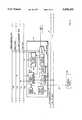
- FIG. 1is a block diagram of a programmable telecommunications switch which resides in a personal computer and which is constructed in accordance with a preferred embodiment of the present invention
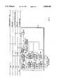
- FIG. 2is a detailed diagram of the CPU/matrix card of FIG. 1;
- FIG. 3is a detailed diagram of the digital line card of FIG. 1;
- FIG. 4is a detailed diagram of the analog line card of FIG. 1.
- FIG. 1shows a commercially available personal computer (PC) 2 which includes a PC central processing unit (CPU) 4 and a hard disk drive 6 interconnected by a PC input/output (I/O) bus 8 and a PC power bus 9.
- the PC 2is preferably a PC-AT®, sold by International Business Machines, or a compatible thereof. Other personal computers having more memory or more powerful CPUs than the PC-AT® may also be used.
- the PC 2preferably operates under an application-oriented operating system, such as DOS® or UNIX®.
- the PC 2consists of a chassis or housing in which a motherboard is mounted, along with the disk drive 6 and other optional assemblies such as floppy disk drives, modems and the like.
- the PC CPU 4is mounted on the motherboard, which includes a series of "slots" into which other boards (cards) may be inserted and thereby connected to the PC I/O and power busses 8 and 9.
- a programmable telecommunication switch 10resides within the PC 2.
- a CPU/matrix card 12is inserted into one of the slots on the motherboard and thus connected to the busses 8 and 9.
- the CPU/matrix card 12is interconnected with a digital (T1) line card 14, a digital signal processing (DSP) card 16 and an analog (universal) line card 18 and a terminator card 19 by four busses: an HDLC or interprocessor bus 20; a TDM bus 22; a line card (LC) status/control bus 24; and a timing/control bus 26.
- a battery/ring voltage bus 28supplies battery voltage (48 VDC) and ringing voltage (109 VAC) to the analog line card 18.
- the terminator card 19serves to physically terminate busses 20, 22, 24, 26 and 28.
- the line cards 14 and 18 and the DSP card 16are all connected to and receive their basic operating power from the PC power bus 9. Although only one digital line card 14 and one analog line card 18 are depicted, it should be understood that additional line cards of either type may be added subject to two physical limitations: (1) the maximum switching capacity of the CPU/matrix card 12, and (2) the physical space within the chassis of the PC 2.
- An external host 30,which may comprise a separate personal computer, workstation or other computer, may optionally be connected via a communication channel 32 to the CPU/matrix card 12.
- the CPU/matrix card 12preferably includes a conventional RS-232 compatible interface for connecting the channel 32.
- the external host 30preferably operates under an application-oriented operating system.
- the switch 10can reside on a passive backplane (no PC CPU 4 or disk 6 present) from which its receives electrical power and be controlled by the external host 30.
- An external battery/ring voltage supply 31is connected via a path 33 to the terminator card 19.
- Supply 31may comprise, for example, a commercially available power supply.
- FIG. 2shows the CPU/matrix card 12 in greater detail.
- a central call processor 34is connected to both the HDLC bus 20 and the LC status/control bus 24.
- the central call processor 34is also connected with host select circuitry 35, random access and read only memories 36, watchdog timing circuitry 38, input/output (I/O) control circuitry 40, timing and control/select circuitry 42 and a time slot interchange (TSI) 44.
- Timing and control/select circuitry 42is connected to the TSI 44, the timing/control bus 26 (for loop timing) and to three sources of timing signals, which are denoted REF 1, REF 2 (which may be supplied by external sources for reference timing) and OSCILLATOR (which may be supplied by a free running oscillator located on the CPU/matrix card 12), respectively.
- the central call processor 34which is preferably a Motorola 68302 microprocessor, has control over all of the other circuitry on the CPU/matrix card 12.
- the central call processor 34preferably runs under a real time operating system such as pSOS®, sold by Integrated Systems, and preferably uses Q.931-1ike messages, a CCITT standard protocol, for communicating over the HDLC bus 20.
- the central call processor 34may transmit a message simultaneously to all cards connected to that bus.
- the processor 34may use the LC status/control bus 24 to select a particular card to transmit a message over the HDLC bus 20.
- the host select circuitry 35which is preferably a switch, operates to inform the processor 34 whether to communicate with the internal hot or the external host upon power-up.
- I/O control circuitry 40which manages all communication between the central call processor 34 and the internal host, preferably appears as a COMM port or other standard PC I/O port on the PC I/O bus 8.
- Timing and control/select circuitry 42operates in response to instructions from the central call processor 34 to select one of five available signals for synchronizing the CPU/matrix card 12. Two such signals are provided by the timing/control bus 26, the other three being REF 1, REF 2 and OSCILLATOR.
- TSI 44which is preferably a 512 port non-blocking matrix, receives incoming PCM voice data via the TDM bus 22 (time slots) and operates, as directed by the central call processor 34, to reorder the time slots and direct them over the bus 22 to the appropriate destinations.
- FIG. 3shows the digital line card 14 of FIG. 1 in greater detail.
- the line card 14includes a line card processor 46 which is connected with the HDLC bus 20, random access and read only memories 48, digital select circuitry 50, HDLC select circuitry 51, elastic stores 52a-52n, dual framers 54a-54n and dual T1 interfaces (IF) 56a-56n.
- Timing and control circuitry 54is connected to the timing and control bus 26, identification (ID) circuitry 49, the digital select circuitry 50, the elastic stores 52a-52n, the dual framers 54a-54n and the dual T1 interfaces 56a-56n.
- IDidentification
- Line card processor 46which is preferably a Motorola 68302 microprocessor, has control over the other circuitry on line card 14.
- Processor 46communicates with the central call processor 34 on the CPU/matrix card 12 by exchanging messages over the HDLC bus 20.
- HDLC select circuitry 51under the control of processor 46, is responsible for controlling the transmission of messages by the line card 14 over the HDLC bus 20.
- Digital select circuitry 50is responsible for moving PCM traffic between the TDM bus 22 and the elastic stores 52a-52n.
- the PCM trafficrepresents only voice, tone or data and does not include any line signalling information.
- Each dual T1 interface 56a-56nis capable of terminating two T1 spans, thus providing a maximum of 96 DS0 ports, out of the total of 512 ports available on the CPU/matrix card 12, per digital line card 14.
- analog line card 18includes timing and control circuitry 58, which is connected to the LC status/control bus 24, the timing/control bus 26, digital select circuitry 60 and identification (ID) circuitry 64, which is similar to ID circuitry 49 of FIG. 3.
- Digital select circuitry 60is connected to analog interfaces 62a-62n.
- LC status/control bus 24 and battery/ring voltage bus 28are connected to each analog interface 62a-62n.
- Timing and control circuitry 58communicates with the central call processor 34 on CPU/matrix card 12 via the LC status/control bus 24.
- Digital select circuitry 60is responsible for moving PCM traffic between the TDM bus 22 and the analog interfaces 62a-62n.
- the PCM traffic between the analog line card 18 and the TDM busmay also contain line signalling information such as on-hook/off-hook, in addition to voice, tone signalling (in-band signalling) or data.
- Analog interfaces 62a-62nare preferably separate physical modules which may be individually installed on the analog line card 18. Such separate modules may support different signalling protocols, thereby advantageously allowing different types of trunks to be terminated on a single analog line card 18.
- the operation of the programmable switch 10will be described.
- the switch 10When the switch 10 is initially powered up (i.e., the PC 2 is turned on), basic configuration information and operational system software must be downloaded from a host before initialization procedures or any call processing operations may commence.
- the CPU/matrix card 12knows whether to request a download from the internal host or the external host based on the setting of the host select circuitry 35. After a successful download is completed, the selection of either the internal host or the external host may be made using messages between the host and switch 10.
- the memory 36is preferably provided with battery-backup in order to preserve the configuration information and eliminate the need for re-downloading in the future should the switch 10 experience a power loss.
- the configuration informationtypically includes basic instructions as to how to control each type of port that the switch may have. Such instructions are stored in memory 36 on the CPU/matrix card 36 for all analog ports, but are downloaded and stored in memory 48 on the digital line card 14 for digital ports, as described below. Such information also preferably includes synchronization priority information which specifies an order in which the five possible synchronization signals available to the timing and control/select circuitry 42 should be used to synchronize the CPU/matrix card 12.
- the central call processor 34proceeds to interrogate all other cards present within the switch 10.
- the processor 34uses the LC status/control bus 24 to interrogate all line cards, both digital and analog, and to receive responses from their respective ID circuitry. These responses indicate to the processor 34 what types and the number of line cards present.
- the central call processor 34will further interrogate the identified analog line cards 18, again using the LC status/control bus 24.
- the analog interfaces 62a-62nidentify the types of modules (signalling protocols) they represent, the number of modules, etc. This information is retained in the memory 36 on the CPU/matrix card 12.
- the central call processor 34further interrogates identified digital line cards 14 using the HDLC bus 20.
- the processor 34transmits a message via the HDLC bus 20 and the digital line card 14 responds with a message indicating the line card's status, how many ports are provided on the card and other information such as whether a download of basic instructions is needed. If a download is needed (requested by the line card 14), the central call processor 34 will respond by passing the appropriate information, previously received from the host, to the line card processor 46 via the HDLC bus 20.
- the central call processor 34constructs a map or table which includes the PCM address range, type of line card and status and type of each port within the switch 10.
- the central call processor 34will proceed to delegate appropriate call processing tasks to that line card's processor 46.
- delegated tasksinclude signalling supervision, call inpulsing and outpulsing, instruction control and management, detection of incoming calls and generation of outgoing calls.
- the switch 10is ready to begin normal operation in accordance with messages received by the CPU/matrix card 12 from the host and activity at the ports.
Landscapes
- Engineering & Computer Science (AREA)
- Computer Networks & Wireless Communication (AREA)
- Physics & Mathematics (AREA)
- Astronomy & Astrophysics (AREA)
- General Physics & Mathematics (AREA)
- Exchange Systems With Centralized Control (AREA)
- Telephonic Communication Services (AREA)
- Data Exchanges In Wide-Area Networks (AREA)
- Electronic Switches (AREA)
- Mobile Radio Communication Systems (AREA)
- Sub-Exchange Stations And Push- Button Telephones (AREA)
- Selective Calling Equipment (AREA)
- Computer And Data Communications (AREA)
- Circuits Of Receivers In General (AREA)
- Input Circuits Of Receivers And Coupling Of Receivers And Audio Equipment (AREA)
- Facsimiles In General (AREA)
- Channel Selection Circuits, Automatic Tuning Circuits (AREA)
Abstract
Description
Claims (28)
Priority Applications (1)
| Application Number | Priority Date | Filing Date | Title |
|---|---|---|---|
| US08/651,123US5598409A (en) | 1992-09-29 | 1996-05-21 | Programmable telecommunications switch for personal computer |
Applications Claiming Priority (4)
| Application Number | Priority Date | Filing Date | Title |
|---|---|---|---|
| US07/953,690US5321744A (en) | 1992-09-29 | 1992-09-29 | Programmable telecommunication switch for personal computer |
| US21669294A | 1994-03-23 | 1994-03-23 | |
| US35058994A | 1994-12-06 | 1994-12-06 | |
| US08/651,123US5598409A (en) | 1992-09-29 | 1996-05-21 | Programmable telecommunications switch for personal computer |
Related Parent Applications (1)
| Application Number | Title | Priority Date | Filing Date |
|---|---|---|---|
| US35058994AContinuation | 1992-09-29 | 1994-12-06 |
Publications (1)
| Publication Number | Publication Date |
|---|---|
| US5598409Atrue US5598409A (en) | 1997-01-28 |
Family
ID=25494401
Family Applications (2)
| Application Number | Title | Priority Date | Filing Date |
|---|---|---|---|
| US07/953,690Expired - LifetimeUS5321744A (en) | 1992-09-29 | 1992-09-29 | Programmable telecommunication switch for personal computer |
| US08/651,123Expired - LifetimeUS5598409A (en) | 1992-09-29 | 1996-05-21 | Programmable telecommunications switch for personal computer |
Family Applications Before (1)
| Application Number | Title | Priority Date | Filing Date |
|---|---|---|---|
| US07/953,690Expired - LifetimeUS5321744A (en) | 1992-09-29 | 1992-09-29 | Programmable telecommunication switch for personal computer |
Country Status (12)
| Country | Link |
|---|---|
| US (2) | US5321744A (en) |
| EP (1) | EP0663135B1 (en) |
| JP (1) | JP3067803B2 (en) |
| AT (1) | ATE163247T1 (en) |
| AU (1) | AU680432B2 (en) |
| BR (1) | BR9307143A (en) |
| CA (1) | CA2145396A1 (en) |
| DE (1) | DE69316987T2 (en) |
| DK (1) | DK0663135T3 (en) |
| ES (1) | ES2111773T3 (en) |
| GR (1) | GR3026111T3 (en) |
| WO (1) | WO1994008430A1 (en) |
Cited By (16)
| Publication number | Priority date | Publication date | Assignee | Title |
|---|---|---|---|---|
| US5826030A (en)* | 1995-11-30 | 1998-10-20 | Excel Switching Corporation | Telecommunication switch having a universal API with a single call processing message including user-definable data and response message each having a generic format |
| US5875234A (en)* | 1996-02-14 | 1999-02-23 | Netphone, Inc. | Computer integrated PBX system |
| US6088749A (en)* | 1995-11-30 | 2000-07-11 | Excel Switching Corp. | Universal API with generic call processing message having user-defined PPL event ID and generic response message for communications between telecommunications switch and host application |
| US6249825B1 (en)* | 1997-07-02 | 2001-06-19 | Cypress Semiconductor | Universal serial bus interface system and method |
| US6252944B1 (en)* | 1997-06-11 | 2001-06-26 | Estech Systems, Inc. | Telephone call/voice processing system |
| US6381239B1 (en) | 1996-02-13 | 2002-04-30 | Taqua Systems, Inc. | Multiple application switching platform and method |
| US6754725B1 (en) | 2001-05-07 | 2004-06-22 | Cypress Semiconductor Corp. | USB peripheral containing its own device driver |
| WO2004073027A3 (en)* | 2003-02-06 | 2005-06-09 | Transwitch Corp | Microprocessor based self-diagnostic port |
| US6978309B1 (en)* | 2000-07-31 | 2005-12-20 | Cisco Technology, Inc. | Method and system for reprogramming instructions for a switch |
| USRE39722E1 (en)* | 1996-06-12 | 2007-07-10 | Estech Systems, Inc. | Telephone call/voice processing system |
| US20090055569A1 (en)* | 2007-08-24 | 2009-02-26 | Cypress Semiconductor Corporation, A Corporation Of The State Of Delaware | Bridge device with page-access based processor interface |
| US7653123B1 (en) | 2004-09-24 | 2010-01-26 | Cypress Semiconductor Corporation | Dynamic data rate using multiplicative PN-codes |
| US7689724B1 (en) | 2002-08-16 | 2010-03-30 | Cypress Semiconductor Corporation | Apparatus, system and method for sharing data from a device between multiple computers |
| US7765344B2 (en) | 2002-09-27 | 2010-07-27 | Cypress Semiconductor Corporation | Apparatus and method for dynamically providing hub or host operations |
| US8090894B1 (en) | 2007-09-21 | 2012-01-03 | Cypress Semiconductor Corporation | Architectures for supporting communication and access between multiple host devices and one or more common functions |
| US8315269B1 (en) | 2007-04-18 | 2012-11-20 | Cypress Semiconductor Corporation | Device, method, and protocol for data transfer between host device and device having storage interface |
Families Citing this family (11)
| Publication number | Priority date | Publication date | Assignee | Title |
|---|---|---|---|---|
| US5463684A (en)* | 1993-11-03 | 1995-10-31 | Microlog Corporation | Telecommunications system for transferring calls without a private branch exchange |
| US5455827A (en)* | 1994-02-23 | 1995-10-03 | Harris Corporation | Multi-processing and direct routing of signalling protocols in voice communication channels |
| AU1883995A (en)* | 1994-03-08 | 1995-09-25 | Excel, Inc. | Telecommunications switch with improved redundancy |
| PT691796E (en)* | 1994-07-07 | 2001-09-28 | Siemens Schweiz Ag | NETWORK TERMINAL DEVICE |
| FR2733868B1 (en)* | 1995-05-03 | 1997-07-04 | Alsacienne Et Lorraine De Tele | ADAPTABLE MODULAR DEVICE FOR INTERCONNECTING OR COMMUNICATING DIFFERENT LOCAL COMPUTER AND / OR COMMUNICATION DEVICES OR NETWORKS AND A METHOD IMPLEMENTING THIS DEVICE |
| JP3115237B2 (en)* | 1996-09-03 | 2000-12-04 | 株式会社東芝 | Control program creation device and control program creation method |
| US5920546A (en)* | 1997-02-28 | 1999-07-06 | Excel Switching Corporation | Method and apparatus for conferencing in an expandable telecommunications system |
| EP1021757A1 (en)* | 1997-07-25 | 2000-07-26 | Starvox, Inc. | Apparatus and method for integrated voice gateway |
| US6594685B1 (en) | 1999-04-14 | 2003-07-15 | Excel Switching Corporation | Universal application programming interface having generic message format |
| KR100394017B1 (en)* | 2001-07-24 | 2003-08-09 | 엘지전자 주식회사 | internet telephony gateway system |
| US8075304B2 (en)* | 2006-10-19 | 2011-12-13 | Wayne/Scott Fetzer Company | Modulated power burner system and method |
Citations (16)
| Publication number | Priority date | Publication date | Assignee | Title |
|---|---|---|---|---|
| DE358597C (en)* | 1920-05-06 | 1922-09-12 | Oskar Zipfler | Collapsible square for tailors |
| US4009337A (en)* | 1973-10-16 | 1977-02-22 | Oki Electric Industry Company, Ltd. | Stored program control type electronic exchange system |
| US4228536A (en)* | 1979-05-29 | 1980-10-14 | Redcom Laboratories, Inc. | Time division digital communication system |
| JPS5869193A (en)* | 1981-10-21 | 1983-04-25 | Hitachi Ltd | Telephone exchange |
| US4527012A (en)* | 1983-01-31 | 1985-07-02 | Redcom Laboratories Inc. | Communications switching system with modular switching communications peripheral and host computer |
| EP0192894A2 (en)* | 1985-01-31 | 1986-09-03 | Ing. C. Olivetti & C., S.p.A. | Integrated office automation system |
| DE3534918A1 (en)* | 1985-09-30 | 1987-04-02 | Siemens Ag | COMPUTER-CONTROLLED SUBSCRIBE SYSTEM |
| US4736406A (en)* | 1986-05-12 | 1988-04-05 | Trillium Telephone Systems Inc. | Expansion subsystem for use in a communication system |
| US4736409A (en)* | 1985-09-02 | 1988-04-05 | Kabushiki Kaisha Toshiba | Control data transmission system for private branch exchange |
| EP0350402A1 (en)* | 1988-07-08 | 1990-01-10 | Js Telecom | Personal computer integrating a digital ISDN subscriber terminal |
| US4908850A (en)* | 1988-01-11 | 1990-03-13 | American Communications & Engineering, Inc. | Voice services network with automated billing |
| US4916726A (en)* | 1988-09-29 | 1990-04-10 | American Tel-A-System, Inc. | Telephone answering service with integrated voice and textual message storage |
| US4955054A (en)* | 1988-10-05 | 1990-09-04 | Precision Software Incorporated | Integrated telecommunication system with improved digital voice response |
| US4993017A (en)* | 1988-03-15 | 1991-02-12 | Siemens Aktiengesellschaft | Modularly structured ISDN communication system |
| US5007080A (en)* | 1988-02-04 | 1991-04-09 | Mitel Corporation | Communication system supporting remote operations |
| DE4101885A1 (en)* | 1991-01-23 | 1992-07-30 | Standard Elektrik Lorenz Ag | Computer-supported telecommunication system - has external computing interface which is available for special services or alarm functions as distinct from e.g. ordinary telephonic communications |
Family Cites Families (1)
| Publication number | Priority date | Publication date | Assignee | Title |
|---|---|---|---|---|
| EP0358597A3 (en)* | 1988-09-07 | 1990-12-12 | ELMEG GmbH Kommunikationstechnik | Telephone exchange |
- 1992
- 1992-09-29USUS07/953,690patent/US5321744A/ennot_activeExpired - Lifetime
- 1993
- 1993-09-15CACA002145396Apatent/CA2145396A1/ennot_activeAbandoned
- 1993-09-15BRBR9307143Apatent/BR9307143A/ennot_activeIP Right Cessation
- 1993-09-15JPJP6509092Apatent/JP3067803B2/ennot_activeExpired - Fee Related
- 1993-09-15AUAU49242/93Apatent/AU680432B2/ennot_activeCeased
- 1993-09-15EPEP93921605Apatent/EP0663135B1/ennot_activeExpired - Lifetime
- 1993-09-15DEDE69316987Tpatent/DE69316987T2/ennot_activeExpired - Lifetime
- 1993-09-15WOPCT/US1993/008724patent/WO1994008430A1/enactiveIP Right Grant
- 1993-09-15ESES93921605Tpatent/ES2111773T3/ennot_activeExpired - Lifetime
- 1993-09-15ATAT93921605Tpatent/ATE163247T1/ennot_activeIP Right Cessation
- 1993-09-15DKDK93921605Tpatent/DK0663135T3/enactive
- 1996
- 1996-05-21USUS08/651,123patent/US5598409A/ennot_activeExpired - Lifetime
- 1998
- 1998-02-12GRGR980400283Tpatent/GR3026111T3/enunknown
Patent Citations (20)
| Publication number | Priority date | Publication date | Assignee | Title |
|---|---|---|---|---|
| DE358597C (en)* | 1920-05-06 | 1922-09-12 | Oskar Zipfler | Collapsible square for tailors |
| US4009337A (en)* | 1973-10-16 | 1977-02-22 | Oki Electric Industry Company, Ltd. | Stored program control type electronic exchange system |
| US4228536A (en)* | 1979-05-29 | 1980-10-14 | Redcom Laboratories, Inc. | Time division digital communication system |
| JPS5869193A (en)* | 1981-10-21 | 1983-04-25 | Hitachi Ltd | Telephone exchange |
| US4527012A (en)* | 1983-01-31 | 1985-07-02 | Redcom Laboratories Inc. | Communications switching system with modular switching communications peripheral and host computer |
| US4527012B1 (en)* | 1983-01-31 | 1994-12-13 | Redcom Laboraties Inc | Communications switching system with modular switching communicatons peripheral and host computer |
| EP0192894A2 (en)* | 1985-01-31 | 1986-09-03 | Ing. C. Olivetti & C., S.p.A. | Integrated office automation system |
| US4736409A (en)* | 1985-09-02 | 1988-04-05 | Kabushiki Kaisha Toshiba | Control data transmission system for private branch exchange |
| DE3534918A1 (en)* | 1985-09-30 | 1987-04-02 | Siemens Ag | COMPUTER-CONTROLLED SUBSCRIBE SYSTEM |
| US4736406A (en)* | 1986-05-12 | 1988-04-05 | Trillium Telephone Systems Inc. | Expansion subsystem for use in a communication system |
| US4908850A (en)* | 1988-01-11 | 1990-03-13 | American Communications & Engineering, Inc. | Voice services network with automated billing |
| US4908850B1 (en)* | 1988-01-11 | 1995-02-07 | American Communications & Engi | Voice services network with automated billing |
| US5007080A (en)* | 1988-02-04 | 1991-04-09 | Mitel Corporation | Communication system supporting remote operations |
| US4993017A (en)* | 1988-03-15 | 1991-02-12 | Siemens Aktiengesellschaft | Modularly structured ISDN communication system |
| US5014269A (en)* | 1988-07-08 | 1991-05-07 | J. S. Telecommunications | Microcomputer integrating a digital subscriber terminal for an integrated service digital network |
| EP0350402A1 (en)* | 1988-07-08 | 1990-01-10 | Js Telecom | Personal computer integrating a digital ISDN subscriber terminal |
| US4916726A (en)* | 1988-09-29 | 1990-04-10 | American Tel-A-System, Inc. | Telephone answering service with integrated voice and textual message storage |
| US4916726B1 (en)* | 1988-09-29 | 1992-06-09 | American Tel A Systems Inc | |
| US4955054A (en)* | 1988-10-05 | 1990-09-04 | Precision Software Incorporated | Integrated telecommunication system with improved digital voice response |
| DE4101885A1 (en)* | 1991-01-23 | 1992-07-30 | Standard Elektrik Lorenz Ag | Computer-supported telecommunication system - has external computing interface which is available for special services or alarm functions as distinct from e.g. ordinary telephonic communications |
Non-Patent Citations (8)
| Title |
|---|
| "Travels," Andy, Marc and Harry, Teleconnect vol. 5 Issue 11 pp. 39-40. |
| Brochure for Model PCX 384 PC Digital Switching Exchange, manufactured and sold by Excel, Inc., Sagamore Beach, MA. Undated.* |
| Brochure for Model PCX-384 PC Digital Switching Exchange, manufactured and sold by Excel, Inc., Sagamore Beach, MA. Undated. |
| IEEE International Conference On Communications ICC 1990 Paper 211.3 vol. 1, 15 Apr. 1990, Atlanta, (US) pp. 128 133 XP147390.* |
| IEEE International Conference On Communications--ICC 1990--Paper 211.3 vol. 1, 15 Apr. 1990, Atlanta, (US) pp. 128-133 XP147390. |
| Travels, Andy, Marc and Harry, Teleconnect vol. 5 Issue 11 pp. 39 40.* |
| User s Manual for Model PCX 384 PC Digital Switching Exchange Undated.* |
| User's Manual for Model PCX-384 PC Digital Switching Exchange Undated. |
Cited By (24)
| Publication number | Priority date | Publication date | Assignee | Title |
|---|---|---|---|---|
| US5826030A (en)* | 1995-11-30 | 1998-10-20 | Excel Switching Corporation | Telecommunication switch having a universal API with a single call processing message including user-definable data and response message each having a generic format |
| US6088749A (en)* | 1995-11-30 | 2000-07-11 | Excel Switching Corp. | Universal API with generic call processing message having user-defined PPL event ID and generic response message for communications between telecommunications switch and host application |
| US6119187A (en)* | 1995-11-30 | 2000-09-12 | Excel Switching Corp. | Telecommunication system with universal API using generic messages having user functionality associated with predetermined functions, primitives and logical states for defining PPL component state machines |
| US6134618A (en)* | 1995-11-30 | 2000-10-17 | Excel Switching Inc. | Telecommunication switch having a universal API with a single call processing message including user-definable data and response message each having a generic format |
| US6381239B1 (en) | 1996-02-13 | 2002-04-30 | Taqua Systems, Inc. | Multiple application switching platform and method |
| US6681001B1 (en) | 1996-02-14 | 2004-01-20 | Nortel Networks Limited | Computer integrated telecommunications systems and methods |
| US5875234A (en)* | 1996-02-14 | 1999-02-23 | Netphone, Inc. | Computer integrated PBX system |
| USRE39722E1 (en)* | 1996-06-12 | 2007-07-10 | Estech Systems, Inc. | Telephone call/voice processing system |
| US8194845B2 (en) | 1996-06-12 | 2012-06-05 | Estech Systems, Inc. | Telephone system |
| US20080317235A1 (en)* | 1996-06-12 | 2008-12-25 | Estech System, Inc. | Telephone system |
| US6252944B1 (en)* | 1997-06-11 | 2001-06-26 | Estech Systems, Inc. | Telephone call/voice processing system |
| US6249825B1 (en)* | 1997-07-02 | 2001-06-19 | Cypress Semiconductor | Universal serial bus interface system and method |
| US6493770B1 (en) | 1997-07-02 | 2002-12-10 | Cypress Semiconductor Corp. | System for reconfiguring a peripheral device by downloading information from a host and electronically simulating a physical disconnection and reconnection to reconfigure the device |
| US6978309B1 (en)* | 2000-07-31 | 2005-12-20 | Cisco Technology, Inc. | Method and system for reprogramming instructions for a switch |
| US7805540B1 (en) | 2000-07-31 | 2010-09-28 | Cisco Technology, Inc. | Method and system for reprogramming instructions for a switch |
| US6754725B1 (en) | 2001-05-07 | 2004-06-22 | Cypress Semiconductor Corp. | USB peripheral containing its own device driver |
| US7689724B1 (en) | 2002-08-16 | 2010-03-30 | Cypress Semiconductor Corporation | Apparatus, system and method for sharing data from a device between multiple computers |
| US7765344B2 (en) | 2002-09-27 | 2010-07-27 | Cypress Semiconductor Corporation | Apparatus and method for dynamically providing hub or host operations |
| WO2004073027A3 (en)* | 2003-02-06 | 2005-06-09 | Transwitch Corp | Microprocessor based self-diagnostic port |
| US7653123B1 (en) | 2004-09-24 | 2010-01-26 | Cypress Semiconductor Corporation | Dynamic data rate using multiplicative PN-codes |
| US8315269B1 (en) | 2007-04-18 | 2012-11-20 | Cypress Semiconductor Corporation | Device, method, and protocol for data transfer between host device and device having storage interface |
| US20090055569A1 (en)* | 2007-08-24 | 2009-02-26 | Cypress Semiconductor Corporation, A Corporation Of The State Of Delaware | Bridge device with page-access based processor interface |
| US8037228B2 (en) | 2007-08-24 | 2011-10-11 | Cypress Semiconductor Corporation | Bridge device with page-access based processor interface |
| US8090894B1 (en) | 2007-09-21 | 2012-01-03 | Cypress Semiconductor Corporation | Architectures for supporting communication and access between multiple host devices and one or more common functions |
Also Published As
| Publication number | Publication date |
|---|---|
| AU680432B2 (en) | 1997-07-31 |
| AU4924293A (en) | 1994-04-26 |
| DK0663135T3 (en) | 1998-09-23 |
| JPH08505271A (en) | 1996-06-04 |
| CA2145396A1 (en) | 1994-04-14 |
| JP3067803B2 (en) | 2000-07-24 |
| DE69316987T2 (en) | 1998-07-09 |
| BR9307143A (en) | 1999-05-25 |
| DE69316987D1 (en) | 1998-03-19 |
| EP0663135B1 (en) | 1998-02-11 |
| US5321744A (en) | 1994-06-14 |
| WO1994008430A1 (en) | 1994-04-14 |
| EP0663135A1 (en) | 1995-07-19 |
| ATE163247T1 (en) | 1998-02-15 |
| ES2111773T3 (en) | 1998-03-16 |
| GR3026111T3 (en) | 1998-05-29 |
Similar Documents
| Publication | Publication Date | Title |
|---|---|---|
| US5598409A (en) | Programmable telecommunications switch for personal computer | |
| US5349579A (en) | Telecommunication switch with programmable communications services | |
| US5426694A (en) | Telecommunication switch having programmable network protocols and communications services | |
| CA2211780C (en) | Telecommunications switch having a universal applications program interface for standardized interactive call processing communications | |
| US5291479A (en) | Modular user programmable telecommunications system with distributed processing | |
| JP3798431B2 (en) | Redundant configuration for telecommunications systems | |
| US6088749A (en) | Universal API with generic call processing message having user-defined PPL event ID and generic response message for communications between telecommunications switch and host application | |
| US6594685B1 (en) | Universal application programming interface having generic message format | |
| US6047384A (en) | Rapid recovery and start-up system for peripheral systems | |
| EP0884883A2 (en) | Improvements in local exchange testing | |
| WO1999035568A2 (en) | Isolation of resources from application in a process control system | |
| JPH033451A (en) | Isdn packet switching system |
Legal Events
| Date | Code | Title | Description |
|---|---|---|---|
| STCF | Information on status: patent grant | Free format text:PATENTED CASE | |
| AS | Assignment | Owner name:EXCEL SWITCHING CORPORATION, MASSACHUSETTS Free format text:CHANGE OF NAME;ASSIGNOR:EXCEL, INC.;REEL/FRAME:008855/0605 Effective date:19970916 | |
| FEPP | Fee payment procedure | Free format text:PAT HLDR NO LONGER CLAIMS SMALL ENT STAT AS INDIV INVENTOR (ORIGINAL EVENT CODE: LSM1); ENTITY STATUS OF PATENT OWNER: LARGE ENTITY | |
| FEPP | Fee payment procedure | Free format text:PAYOR NUMBER ASSIGNED (ORIGINAL EVENT CODE: ASPN); ENTITY STATUS OF PATENT OWNER: LARGE ENTITY | |
| FPAY | Fee payment | Year of fee payment:4 | |
| FEPP | Fee payment procedure | Free format text:PAYOR NUMBER ASSIGNED (ORIGINAL EVENT CODE: ASPN); ENTITY STATUS OF PATENT OWNER: LARGE ENTITY Free format text:PAYER NUMBER DE-ASSIGNED (ORIGINAL EVENT CODE: RMPN); ENTITY STATUS OF PATENT OWNER: LARGE ENTITY | |
| FPAY | Fee payment | Year of fee payment:8 | |
| AS | Assignment | Owner name:EXCEL SWITCHING CORPORATION, MASSACHUSETTS Free format text:RELEASE BY SECURED PARTY;ASSIGNOR:COMERICA BANK;REEL/FRAME:019920/0425 Effective date:20060615 Owner name:BROOKTROUT, INC, MASSACHUSETTS Free format text:RELEASE BY SECURED PARTY;ASSIGNOR:COMERICA BANK;REEL/FRAME:019920/0425 Effective date:20060615 Owner name:EAS GROUP, INC., MASSACHUSETTS Free format text:RELEASE BY SECURED PARTY;ASSIGNOR:COMERICA BANK;REEL/FRAME:019920/0425 Effective date:20060615 | |
| FPAY | Fee payment | Year of fee payment:12 |