US5598346A - Array of configurable logic blocks including network means for broadcasting clock signals to different pluralities of logic blocks - Google Patents
Array of configurable logic blocks including network means for broadcasting clock signals to different pluralities of logic blocksDownload PDFInfo
- Publication number
- US5598346A US5598346AUS08/596,679US59667996AUS5598346AUS 5598346 AUS5598346 AUS 5598346AUS 59667996 AUS59667996 AUS 59667996AUS 5598346 AUS5598346 AUS 5598346A
- Authority
- US
- United States
- Prior art keywords
- clock
- output
- input
- line
- broadcasting
- Prior art date
- Legal status (The legal status is an assumption and is not a legal conclusion. Google has not performed a legal analysis and makes no representation as to the accuracy of the status listed.)
- Expired - Fee Related
Links
- 230000006870functionEffects0.000claimsdescription50
- 230000008878couplingEffects0.000claimsdescription7
- 238000010168coupling processMethods0.000claimsdescription7
- 238000005859coupling reactionMethods0.000claimsdescription7
- 238000012545processingMethods0.000claimsdescription4
- 239000002243precursorSubstances0.000claims3
- 239000000872bufferSubstances0.000description140
- 210000004027cellAnatomy0.000description103
- 230000002457bidirectional effectEffects0.000description48
- 230000004044responseEffects0.000description38
- 238000010586diagramMethods0.000description27
- 239000011159matrix materialSubstances0.000description26
- 238000003491arrayMethods0.000description14
- 230000002093peripheral effectEffects0.000description10
- 238000003860storageMethods0.000description10
- 238000013461designMethods0.000description9
- 230000000295complement effectEffects0.000description8
- 229920000954PolyglycolidePolymers0.000description3
- PWPJGUXAGUPAHP-UHFFFAOYSA-NlufenuronChemical compoundC1=C(Cl)C(OC(F)(F)C(C(F)(F)F)F)=CC(Cl)=C1NC(=O)NC(=O)C1=C(F)C=CC=C1FPWPJGUXAGUPAHP-UHFFFAOYSA-N0.000description3
- 235000010409propane-1,2-diol alginateNutrition0.000description3
- 238000012552reviewMethods0.000description3
- 210000000352storage cellAnatomy0.000description3
- 230000008901benefitEffects0.000description2
- 239000003990capacitorSubstances0.000description2
- 230000008859changeEffects0.000description2
- 239000013078crystalSubstances0.000description2
- 230000001934delayEffects0.000description2
- 230000000694effectsEffects0.000description2
- 239000002184metalSubstances0.000description2
- 238000000034methodMethods0.000description2
- 239000000203mixtureSubstances0.000description2
- 238000012986modificationMethods0.000description2
- 230000004048modificationEffects0.000description2
- 230000036316preloadEffects0.000description2
- 230000000644propagated effectEffects0.000description2
- 230000001902propagating effectEffects0.000description2
- XUIMIQQOPSSXEZ-UHFFFAOYSA-NSiliconChemical compound[Si]XUIMIQQOPSSXEZ-UHFFFAOYSA-N0.000description1
- 230000003750conditioning effectEffects0.000description1
- 230000001276controlling effectEffects0.000description1
- 230000002596correlated effectEffects0.000description1
- 238000009826distributionMethods0.000description1
- 238000005516engineering processMethods0.000description1
- 230000007274generation of a signal involved in cell-cell signalingEffects0.000description1
- 230000036039immunityEffects0.000description1
- 238000004519manufacturing processMethods0.000description1
- 230000005055memory storageEffects0.000description1
- 230000008569processEffects0.000description1
- 230000000630rising effectEffects0.000description1
- 229910052710siliconInorganic materials0.000description1
- 239000010703siliconSubstances0.000description1
- 230000003068static effectEffects0.000description1
- 230000001360synchronised effectEffects0.000description1
Images


Classifications
- H—ELECTRICITY
- H03—ELECTRONIC CIRCUITRY
- H03K—PULSE TECHNIQUE
- H03K19/00—Logic circuits, i.e. having at least two inputs acting on one output; Inverting circuits
- H03K19/02—Logic circuits, i.e. having at least two inputs acting on one output; Inverting circuits using specified components
- H03K19/173—Logic circuits, i.e. having at least two inputs acting on one output; Inverting circuits using specified components using elementary logic circuits as components
- H03K19/177—Logic circuits, i.e. having at least two inputs acting on one output; Inverting circuits using specified components using elementary logic circuits as components arranged in matrix form
- H03K19/17736—Structural details of routing resources
- H—ELECTRICITY
- H03—ELECTRONIC CIRCUITRY
- H03K—PULSE TECHNIQUE
- H03K19/00—Logic circuits, i.e. having at least two inputs acting on one output; Inverting circuits
- H03K19/02—Logic circuits, i.e. having at least two inputs acting on one output; Inverting circuits using specified components
- H03K19/173—Logic circuits, i.e. having at least two inputs acting on one output; Inverting circuits using specified components using elementary logic circuits as components
- H03K19/1733—Controllable logic circuits
- H03K19/1737—Controllable logic circuits using multiplexers
- H—ELECTRICITY
- H03—ELECTRONIC CIRCUITRY
- H03K—PULSE TECHNIQUE
- H03K19/00—Logic circuits, i.e. having at least two inputs acting on one output; Inverting circuits
- H03K19/02—Logic circuits, i.e. having at least two inputs acting on one output; Inverting circuits using specified components
- H03K19/173—Logic circuits, i.e. having at least two inputs acting on one output; Inverting circuits using specified components using elementary logic circuits as components
- H03K19/177—Logic circuits, i.e. having at least two inputs acting on one output; Inverting circuits using specified components using elementary logic circuits as components arranged in matrix form
- H03K19/17704—Logic circuits, i.e. having at least two inputs acting on one output; Inverting circuits using specified components using elementary logic circuits as components arranged in matrix form the logic functions being realised by the interconnection of rows and columns
- H—ELECTRICITY
- H03—ELECTRONIC CIRCUITRY
- H03K—PULSE TECHNIQUE
- H03K19/00—Logic circuits, i.e. having at least two inputs acting on one output; Inverting circuits
- H03K19/02—Logic circuits, i.e. having at least two inputs acting on one output; Inverting circuits using specified components
- H03K19/173—Logic circuits, i.e. having at least two inputs acting on one output; Inverting circuits using specified components using elementary logic circuits as components
- H03K19/177—Logic circuits, i.e. having at least two inputs acting on one output; Inverting circuits using specified components using elementary logic circuits as components arranged in matrix form
- H03K19/17724—Structural details of logic blocks
- H03K19/17728—Reconfigurable logic blocks, e.g. lookup tables
- H—ELECTRICITY
- H03—ELECTRONIC CIRCUITRY
- H03K—PULSE TECHNIQUE
- H03K19/00—Logic circuits, i.e. having at least two inputs acting on one output; Inverting circuits
- H03K19/02—Logic circuits, i.e. having at least two inputs acting on one output; Inverting circuits using specified components
- H03K19/173—Logic circuits, i.e. having at least two inputs acting on one output; Inverting circuits using specified components using elementary logic circuits as components
- H03K19/177—Logic circuits, i.e. having at least two inputs acting on one output; Inverting circuits using specified components using elementary logic circuits as components arranged in matrix form
- H03K19/17724—Structural details of logic blocks
- H03K19/17732—Macroblocks
- H—ELECTRICITY
- H03—ELECTRONIC CIRCUITRY
- H03K—PULSE TECHNIQUE
- H03K19/00—Logic circuits, i.e. having at least two inputs acting on one output; Inverting circuits
- H03K19/02—Logic circuits, i.e. having at least two inputs acting on one output; Inverting circuits using specified components
- H03K19/173—Logic circuits, i.e. having at least two inputs acting on one output; Inverting circuits using specified components using elementary logic circuits as components
- H03K19/177—Logic circuits, i.e. having at least two inputs acting on one output; Inverting circuits using specified components using elementary logic circuits as components arranged in matrix form
- H03K19/17736—Structural details of routing resources
- H03K19/17744—Structural details of routing resources for input/output signals
Definitions
- the present inventionrelates generally to programmable logic devices and, more particularly, to programmable gate arrays consisting of an array of logic blocks and input/output blocks with an interconnection structure, each of which are configurable by a configuration program stored in on chip memory.
- the programmable gate arrayis a high performance, user programmable device containing three types of configurable elements that are customized to a user system design.
- the three elementsare (1) an array of configurable logic blocks (CLBs), (2) with input/output blocks (IOBs) around a perimeter, all linked by (3) a flexible programmable interconnect network.
- CLBsconfigurable logic blocks
- IOBsinput/output blocks
- the system design desired by a useris implemented in the device by configuring programmable RAM cells. These RAM cells control the logic functionality performed by the CLBs, IOBs and the interconnect.
- the configurationis implemented using PGA design software tools.
- Xilinxoriginally introduced the XC2000 series of logic cell arrays and has more recently introduced a second generation XC3000 family of integrated circuit programmable gate arrays.
- a description of the 2000 series, as well as related programmable logic device art,can be found in THE PROGRAMMABLE GATE ARRAY DESIGN HANDBOOK, First Edition, published by Xilinx, pages 1-1 through 1-31.
- the architecture for the XC3000 familyis provided in a technical data handbook published by Xilinx entitled XC3000 LOGIC CELL ARRAY FAMILY, pages 1-31.
- Each of these Xilinx publicationsis incorporated by reference in this application as providing a description of the prior art.
- the programmable gate arrayconsists of a configurable interconnect, a ring of configurable input/output blocks, and an array of configurable logic blocks. It is the combination of these three major features that provides flexibility and data processing power for programmable gate arrays.
- the programmable gate arrays of the prior artsuffer certain limitations in each of the interconnect structure, the input/output block structures, and the configurable logic block structures.
- the configurable interconnect structuremust provide the ability to form networks on the programmable gate array which optimize utilization of the resources on the chip.
- the prior art interconnect systemshave tended to force connection in the logical network to configurable blocks in a relatively small area. For instance, a prior system provides direct connections only between adjacent configurable logic blocks.
- the inputs and outputs on the configurable logic blocksare arranged in a left to right or otherwise asymmetrical layout that forces signal flow in a certain direction across the chip. This causes congestion on the interconnect structure for applications requiring a large number of inputs or outputs. Also, this forces the printed circuit board layout, which includes one of these asymmetrically designed logic cell arrays, to provide for inputs on one side of the logic cell array and outputs on the other.
- the input/output blocks in the prior art programmable gate arraysare relatively complex macro cells in order to provide flexibility needed for the wide variety of applications intended for the devices.
- these complex macro cellsinclude resources that are unused in many configurations of the input/output blocks.
- the blocksare relatively slow because of the complexity, requiring passage through a number of buffers, multiplexers and registers between the logic cells and the input/output pad.
- the input/output blockscause congestion on the peripheral logic blocks in the device for applications involving a lot of input and output.
- the configurable logic blocksthemselves also suffer limitations which impact the flexibility of the device.
- the logic blocks of the prior arthave operated upon a relatively small set of input variables.
- wide gating functionssuch as decoding a 16 bit instruction or a wide multiplexing function, required cascading of many configurable blocks.
- a very simple functioncan utilize a large number of configurable logic blocks in the array.
- cascading blocksdue to the limitation of the number of direct interconnections between the logic blocks, many of the signals have to be transmitted across the programmable general connect. This causes delay because of the number of programmable interconnection points used. Further, for critical paths requiring fast operation, the cascading of blocks becomes impractical.
- the configurable logic blockstypically four input signals are used for the logic function.
- the configurable logic blocksused a sharing of inputs scheme. This sharing of inputs greatly limits the logic flexibility for these five variable functions in the prior art.
- the present inventionprovides an architecture for a configurable logic array with an interconnect structure which improves flexibility in creating networks to allow for greater utilization of the configurable logic blocks and input/output blocks on the device.
- the present inventionis an improved configurable logic array comprising a configuration memory storing program data specifying a user defined data processing function.
- a plurality of configurable logic blocksare arranged in an array consisting of C columns and R rows.
- Each configurable logic blockis coupled to the configuration memory and has a plurality of inputs and outputs for generating output signals at the respective outputs in response to the input signals at the respective inputs and in response to program data in the configuration store.
- a plurality of configurable input/output blocksis included, each coupled to an input/output pad and to the configuration store, and having at least one input and at least one output.
- the configurable input/output blocksprovide configurable interfaces between the respective pads and the respective inputs and outputs in response to the program data.
- a configurable interconnectis coupled to the configurable logic blocks, configurable input/output blocks and to the configuration store, for connecting the inputs and outputs of configurable logic blocks and configurable input/output blocks into logical networks in response to the program data in the configuration store
- the configurable interconnectis symmetrically disposed relative to the inputs and outputs of the configurable logic blocks.
- inputs of the CLBscan be derived from four sides and outputs can be driven to four sides of the respective CLB into a symmetrical interconnect structure.
- the interconnectincludes a plurality of horizontal buses along the rows of CLBs and a plurality of vertical buses along the columns of CLBs.
- the intersections of the horizontal and vertical busesare configurable to route networks across the device.
- interconnectincludes a plurality of switching matrices at the intersections of horizontal and vertical buses, each having a set of horizontal connections and a set of vertical connections, for interconnecting respective ones of the horizontal or vertical connections in response to program data in the configuration store.
- a plurality of horizontal conductive segments in the horizontal busare connected between the horizontal connections of the switching matrices.
- a plurality of programmable interconnect points coupled to respective inputs and outputs of the configurable logic blocks and input/output blocksprovide connectability to respective horizontal segments in response to program data.
- a plurality of vertical conductive segments in the vertical busare connected between the vertical connections of the adjacent switching matrices.
- Programmable interconnect pointsinterconnect the respective inputs and outputs of configurable logic blocks and input/output blocks with respective vertical segments in response to the program data.
- the vertical and horizontal segmentsare characterized by extending from a switching matrix in a vertical or horizontal bus "i" to switch matrix in bus "i+2", so that each segment spans two columns or rows of logic blocks.
- the buses in the interconnectare further characterized by a plurality of horizontal and vertical long conductive lines which extend across the entire chip.
- Each long lineis connected to a plurality of programmable interconnect points for interconnecting the respective inputs or outputs of configurable logic cells with the respective long line in response to program data in the configuration memory.
- the long linesare characterized by having programmable interconnect points coupling an output of a configurable logic block which is supplied by a tristate buffer to the respective long lines.
- the buses in the interconnect structureare characterized by uncommitted horizontal and vertical long lines.
- Each uncommitted long lineis connected to a first plurality of programmable interconnect points for interconnecting the respective outputs of configurable logic blocks or input/output blocks with the respective long line in response to program data, and a second plurality of programmable interconnect points for interconnecting respective uncommitted long line with the horizontal or vertical segments that are coupled to the switching matrices.
- the interconnect structurefurther includes a plurality of direct connections interconnecting an output of a configurable logic block or input/output block to an input of another configurable logic block or input/output block.
- the direct connectionsare characterized by including at least a first subset which are connected between adjacent input/output blocks or configurable logic blocks, and a second subset which are connected between the output of a configurable logic block or input/output block and a next adjacent configurable logic block or input/output block.
- each CLBis directly connected to 8 neighbor CLBs.
- the plurality of configurable input/output blocksis characterized by groups of input/output blocks associated with each row or column of configurable logic blocks.
- each groupat least one complex input/output block is included and at least one simple input/output block.
- the complex input/output blocksprovide the flexible functionality required for many applications, while the simple input/output block provides a fast access path into or out of the configurable array.
- all of the input/output logic blocksare characterized by tristatable output buffers to pads and to the internal interconnect which are controlled in response to the program data and/or a control signal generated in the configurable logic array.
- the outputs of the configurable logic blocksinclude a plurality of tristate buffers which receive respective ones of the output signals of the combinational logic and tristate control signals.
- the tristate output bufferssupply a respective output signals or present a high impedance state as output from the logic block in response to the tristate control signal.
- the tristate control signalis generated in response to the program data in the configuration store and an input to the configurable logic block.
- Another aspect of the inventionis configurable repowering buffers with a bypass path coupled to the horizontal and vertical segments that go through switching matrices. Also, provision is made through the interconnect to supply control signals to all CLBs in the array from a single source.
- the configurable logic blocksare characterized by a number of improvements over the prior art.
- the configurable logic blocksprovide for a mixture of narrow gating and wide gating functions, which suffer a speed penalty only for the wide gating functions.
- the configurable logic blocksare symmetrical, accepting inputs on four sides of each block and providing outputs on four sides.
- the output structuresthemselves provide the ability for tristating outputs connected to the configurable interconnect, and for directly driving signals to other configurable logic blocks.
- the input structures on all four sides of the configurable logic blocksare independently configurable in response to the configuration program.
- the four output macro cells in each configurable logic blockare independently configurable.
- the registers in each of the output macro cellsare accessible independently of the combinational logic in the configurable logic block. This allows these registers to be used in networks that are independent of the combinational logic.
- the configurable logic blockcan be characterized as having an input multiplexing tree which receives J input signals and selects a subset K signals, where K is less than or equal to J, in response to the program data.
- Combinational logicis coupled to the configuration memory and the input multiplexing tree, for generating a plurality of L logic signals in response to the K signals and the program data.
- Four independent output macro cellsare included, each of which select output signals from the plurality of L logic signals.
- Each of the output macro cellsincludes a tristatable output buffer for driving a selected output signal to the configurable interconnect. Also, each output macro cell includes a second output buffer, for driving a signal that is selected independently of the tristatable output buffer, for driving signals onto direct connections to other configurable logic blocks.
- the input multiplexing treeis characterized by providing that any one of the K signals can be supplied from any of the four sides of the configurable logic block.
- the combinational logicis implemented with a first lookup table in the program data consisting of 64 bits which are grouped into eight 8 bit arrays.
- the 8 bit arraysare paired so that three independently supplied signals from the subset of K signals supplied by the input multiplexing tree are used to address each of the four pairs of 8 bit arrays.
- the two outputs of each pairare coupled to a cross-multiplexer which is configurable in response to the program data to directly pass through the two outputs supplied by the two 8 bit arrays in the pair, or to select one of the two outputs as a primary output in response to a fourth independently supplied signal from the subset K signals.
- the output of the cross-multiplexeris supplied through a third multiplexing level consisting of two multiplexers, each independently controllable by respective ones of the subset of K signals.
- the output of the third level of multiplexingis then supplied to a fourth level of multiplexing which is controlled by one of the subset of K signals, providing output which is a full lookup function of the 64 bit array in response to six inputs.
- the combinational logicfurther includes a special 16 bit array in the program data which is coupled to a sixteen to one multiplexer.
- Control inputs to the sixteen to one multiplexerare the pass through outputs of the four cross-multiplexers referred to above. Each of these inputs is a function of four independent variables.
- the output of the sixteen to one multiplexerprovides a special output, which provides a limited lookup function of the 16 independent variables.
- the special outputis combined with the output of the fourth level multiplexer in a fifth level multiplexer, which is controlled in response to an input signal of the subset of K signals, or by the program data.
- the configurable logic blockis characterized by a preload capability.
- each of the storage elements in the output macro cells of the configurable logic blocksis enabled to receive data as if it were a location in the configuration memory.
- the configurable input/output architectureis characterized by a number of improvements over the prior art.
- the architectureprovides for groups of input/output blocks associated with each row and column of configurable logic blocks in the array.
- Each of the groupsis further characterized by having a plurality of complex input/output blocks, which provide flexible structures for implementing interfaces between the configurable logic array and outside devices, and at least one simple input/output block which provides a fast path from outside the device to the configurable logic array if required by a particular application.
- both the simple and complex input/output blocksare characterized by having at least one tristatable output buffer for driving signals onto the configurable interconnect structure, and a second buffer for driving direct connections to configurable logic blocks in the device.
- the complex input/output blocksinclude an input storage element and an output storage element.
- a direct connectionis provided from the input storage element of one complex input/output cell to a next adjacent complex input/output around the perimeter of the device.
- the output storage elements of the complex input/output cellsare similarly connected.
- the storage elements in the complex input/output blockscan be linked into a configurable data path where they can be operated as a shift register or other similar circuit.
- the storage elements in the complex input/output blocksare further configured to provide for synchronization functions, local readback functions, and buried register functions.
- the input/output blocksare further characterized by control signal generation from the long lines in the programmable interconnect structure. This allows utilization of networks in the configurable logic array to control the operation and configuration of the configurable input/output blocks in a dynamic fashion. Also, the long lines are configured to propagate signals completely around the perimeter of the array, so that a common signal can be used to control all of the input/output blocks.
- the configurable logic arrayprovided, according to the present invention, greatly improves the flexibility and performance of programmable gate arrays over those available in the prior art. This is accomplished in part by an interconnect structure which supports networks with long reach across the device, multi-source networks, and symmetrical connections to the configurable logic blocks.
- a unique configurable logic block architecturesupports efficient utilization of the resources in the array, wide gating functions, narrow gating functions without speed penalty and implementation of symmetrical networks in the array.
- a unique input/output architecturesupports efficient utilization of the resources in the input/output structures, allows for both fast signal propagation through the simple input/output blocks and high function signal propagation through the complex input/output blocks into the array, and has improved flexibility in the source of control signals for the input/output structure.
- FIG. 1is schematic diagram illustrating the layout of the programmable gate array according to the present invention.
- FIG. 2is a schematic diagram of the configuration memory in the programmable gate array according to the present invention.
- FIG. 3is a diagram of the configuration memory storage cell.
- FIG. 4illustrates a notation scheme for vertical buses in the programmable gate array.
- FIG. 5illustrates a notation scheme for the horizontal buses in the programmable gate array.
- FIG. 6illustrates the placement of the switch matrices in lines 5-14 of the horizontal and vertical buses in the programmable gate array.
- FIG. 7illustrates the intersection of a vertical bus with a horizontal bus.
- FIG. 8illustrates an alternative intersection of a vertical bus with a horizontal.
- FIG. 9illustrates the intersection of vertical buses 1 and 9 with even numbered horizontal buses and horizontal buses 1 and 9 with even numbered vertical buses.
- FIG. 10illustrates the intersection of vertical buses 1 and 9 with the odd numbered horizontal buses and horizontal buses 1 and 9 with the odd numbered vertical buses.
- FIG. 11illustrates the intersection of horizontal bus 1 with vertical bus 1 at the corner.
- FIG. 12illustrates the intersection of horizontal bus 1 with vertical bus 9 at the corner.
- FIG. 13illustrates the intersection of horizontal bus 9 with vertical bus 1 at the corner.
- FIG. 14illustrates the intersection of horizontal bus 9 with vertical bus 9 at the corner.
- FIG. 14Aillustrates an alternative corner connection scheme that can be used at all four corner intersections, replacing the schemes of FIGS. 11-14.
- FIG. 15illustrates the connection of lines 16 and 17 of the vertical buses with the global reset and global clock buffers.
- FIG. 15Aillustrates the connection of the vertical lines 16 and 17 with the configurable logic blocks.
- FIG. 15Billustrates the signal path from an input/output pad bypassing internal IOB logic for connection to the global clock buffer, horizontal alternate buffer or vertical alternate buffer.
- FIG. 15Cillustrates the inputs to the global clock buffer.
- FIG. 16illustrates the connection of the horizontal alternate buffers with line 15 on the horizontal buses and the vertical alternate buffers with line 15 on the vertical buses.
- FIG. 16Aillustrates the connection of the input/output blocks and the configurable logic blocks with line 15.
- FIG. 16Billustrates the input paths to the vertical alternate buffer.
- FIG. 16Cillustrates the input paths to the horizontal alternate buffer.
- FIG. 16Dillustrates the crystal oscillator circuit by which the oscillator signal OSC is generated on the chip.
- FIG. 16Eillustrates the external connections for the oscillator of FIG. 16D.
- FIG. 17illustrates one implementation of a programmable interconnect point using bidirectional pass transistors.
- FIG. 18illustrates an alternative configuration of a programmable interconnect point using a unidirectional multiplexer technique.
- FIG. 19illustrates the interconnect structure of the switch matrix.
- FIG. 20illustrates the repowering buffer used in the programmable interconnect.
- FIG. 21shows the switch matrix interconnection options for each connection to the switch matrix.
- FIG. 22illustrates the interconnection in the segment boxes on vertical buses 1 and 9.
- FIG. 23illustrates the interconnection in the segment boxes on horizontal buses 1 and 9.
- FIG. 24illustrates the segment box interconnection options for each connection to the segment box.
- FIG. 25is an overview block diagram of the configurable logic block.
- FIG. 26schematically illustrates the inputs and outputs and provides a notation for the configurable logic block.
- FIG. 27is a schematic diagram of the combinational logic in the configurable logic block.
- FIG. 28is a schematic diagram of the special output stage which is coupled to the combinational logic of FIG. 27.
- FIG. 29is a schematic diagram of the macro cell for outputs X1 and Y1 on the configurable logic block.
- FIG. 29Aillustrates the connection of the register in the macro cell which provides for preload during programming of the configurable logic array.
- FIG. 30is a schematic diagram of the macro cell for outputs X2 and Y2 on the configurable logic block.
- FIG. 31is a schematic diagram of the macro cell for outputs X3 and Y3 on the configurable logic block.
- FIG. 32is a schematic diagram of the macro cell for outputs X4 and Y4 on the configurable logic block.
- FIG. 33is a diagram of the input multiplexing structure for signals VA1-VA4 which are used in the first level multiplexing in the combinational logic section of the configurable logic block.
- FIG. 34is a schematic diagram of the input multiplexing structure for signals VB1-VB4 which are used in the first level multiplexing in the combinational logic section of the configurable logic block.
- FIG. 35is a schematic diagram of the input multiplexer structure for signals VC1-VC4 which are used in the first level multiplexing in the combinational logic section of the configurable logic block.
- FIG. 36is a schematic diagram of the input multiplexing structure for signals VD1-VD4 which are used in the second level multiplexing in the combinational logic section of the configurable logic block.
- FIG. 37is a diagram of the input multiplexing structure for VE1 and VE2 used in the third level multiplexing of the combinational logic.
- FIG. 38is a diagram of the input multiplexing structure for the fourth level multiplexing signal VF in the combinational logic.
- FIG. 39is a schematic diagram of the input multiplexing structure for the control signal VG used in providing the special output.
- FIGS. 40A-40Hshow respectively the input multiplexing for the general purpose control lines CT1-CT8.
- FIG. 41is a schematic diagram of the circuit generating output enable control signals OE1-OE4 in the configurable logic block.
- FIG. 42is a diagram illustrating selection of the clock signal in the configurable logic block.
- FIG. 43is the schematic diagram illustrating generation of the clock enable signal in the configurable logic block.
- FIG. 44is a schematic diagram illustrating selection of the reset signal in the configurable logic block.
- FIG. 45is a schematic diagram of a simple input/output cell according to the present invention.
- FIG. 46is a schematic diagram of a complex input/output cell according to the present invention.
- FIG. 47illustrates the inputs and outputs of the complex input/output block.
- FIG. 48illustrates the inputs and outputs of the simple input/output block.
- FIG. 49schematically illustrates the connection of the complex input/output blocks in a shift register configuration.
- FIG. 50illustrates the direct connections from outputs of next adjacent configurable logic blocks to the inputs of a given logic block.
- FIG. 51illustrates direct connections from adjacent configurable logic blocks to the inputs of the center configurable logic block.
- FIG. 52illustrates direct connections from the output of the center configurable logic block to adjacent and next adjacent configurable logic blocks.
- FIG. 53illustrates direct connection of the outputs X1-X4 on peripheral configurable logic blocks.
- FIG. 54illustrates direct connection to the inputs of a peripheral configurable logic block.
- FIG. 55illustrates direct connections to the inputs F1-F4 on a peripheral configurable logic block.
- FIG. 56illustrates the programmable connections between the interconnect structure and the configurable logic blocks.
- FIG. 57illustrates the fixed connections between the interconnect structure and the configurable logic blocks.
- FIG. 58illustrates the programmable connection of the configurable logic blocks in the array to uncommitted long lines.
- FIG. 59illustrates the programmable connections to the outer long lines from the CLBs.
- FIG. 60illustrates the reach between input/output blocks and configurable logic blocks on long lines.
- FIG. 61illustrates the programmable connections between the input/output blocks on the top side of the configurable array and horizontal bus 1.
- FIG. 62illustrates the programmable connections between horizontal bus 9 and the input/output blocks on the bottom side of the configurable array.
- FIG. 63illustrates the programmable Interconnects between the vertical bus 1 and the input/output blocks on the left side of the array.
- FIG. 64illustrates the programmable interconnects between vertical bus 9 and the input/output blocks on the right side of the array.
- FIG. 65illustrates the connection of the clock and reset signals to the complex logic blocks, as well as the programmable connections of the inputs and the outputs of the input/output blocks on the top side of the array to the vertical buses.
- FIG. 66illustrates the connection of the clock and reset signals to the input/output blocks on the bottom side of the array, and connection of these bottom side input/output blocks to the vertical buses.
- FIG. 67illustrates the connection of the clock and reset signals to the input/output blocks on the left side, and connection of these left side input/output blocks to horizontal buses.
- FIG. 68illustrates the connection of the clock and the reset signals to the input/output blocks on the right side of the array, and connection of these right side input/output blocks to the horizontal buses.
- FIG. 69illustrates the connection of the control signal inputs on the input/output blocks on the top and left side of the array to the adjacent interconnect buses.
- FIG. 70illustrates the connection of the control signal inputs to the input/output blocks on the right and bottom side of the array to the adjacent interconnect buses.
- FIGS. 1-3the basic layout and programming structure of the programmable gate array is described.
- FIGS. 4-24a detailed description of the interconnect structure is set out with reference to FIGS. 4-24.
- Implementation of the configurable logic block utilized in the programmable gate arrayis described with reference to FIGS. 25-44.
- Implementation of the configurable logic blocks utilized in the programmable gate arrayare described with reference to FIGS. 45-49.
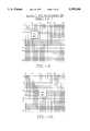
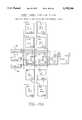
- FIG. 1illustrates the layout of the programmable gate array according to the present invention. Also provided in FIG. 1 is a notation which is utilized to describe the programmable gate array in this application. Accordingly, the programmable gate array shown in FIG. 1 consists of an array of configurable logic blocks illustrated by the square symbol with bold lines shown at the upper left hand corner of the figure. Each configurable logic block in the array is labeled with a row and column number, i.e. in the upper left hand corner of the array, the configurable logic blocks are labeled R1C1, R1C2, and so on until the lower right hand corner of the array where the configurable logic block is labeled R8C8. Around the peripheral of the array are 110 pads for connection to external pins.
- Pads 2-13, 16-27, 29-40, 43-54, 57-68, 71-82, 85-96 and 99-110are coupled to configurable input/output blocks represented by the symbol shown in the upper left hand corner of the FIG.
- Pads 1, 14, 15, 28, 41, 42, 55, 56, 69, 70, 83, 84, 79 and 98are utilized for functions other than configurable input/output blocks, such as power, ground, global clock and reset signal inputs, and programming mode control signals.
- the connection of these miscellaneous padsis similar to that done in prior art programmable gate array and is not further described here.
- the interconnect structureconsists of nine horizontal buses labeled HBUS1 through HBUS9 with nine intersecting vertical buses VBUS1 through VBUS9.
- the intersections of vertical bus 1 and vertical bus 9 with the horizontal buses 2-8are characterized by having segment boxes which provide programmable interconnection between the respective horizontal bus and the vertical bus as described in detail below.
- the intersections of horizontal bus 1 and horizontal bus 9 with vertical buses 2-8are characterized by segment boxes providing the programmable interconnection between the horizontal and vertical buses.
- intersections of the vertical buses 2-8 with the horizontal buses 2-8are characterized by switching matrices providing for interconnection between the respective horizontal and vertical buses.
- the placement of the segment boxes and switching matricesis schematically illustrated in FIG. 1 using the symbols illustrated in the lower left hand corner of the Figure. The detailed structure of the switching matrices and segment boxes is described below.
- the programmable gate array according to the present inventioncontains three types of configurable elements that are customized to a user system design which is specified in a configuration memory.
- the three configurable elementsare the array of configurable logic blocks (CLBs), the configurable input/output blocks (IOBs) around the perimeter, and the programmable interconnect network.
- CLBsconfigurable logic blocks
- IOBsconfigurable input/output blocks
- the system design of a useris implemented in the programmable gate array by configuring programmable RAM cells known as a configuration memory. These RAM cells control the logic functionality performed by the CLBs, IOBs, and the interconnect.
- the loading of the configuration memoryis implemented using a set of design software tools as well known in the art.
- the perimeter of configurable IOBsprovide a programmable interface between the internal logic array and device package pins.
- the array of CLBsperform user specified logic functions.
- the interconnectionconsists of direct connections between specific CLBs or IOBs, and a general connect that is programmed to form networks carrying logic signals among the blocks.
- CLBsThe logic functions performed by the CLBs are determined by programmed lookup tables in the configuration memory. Functional options are performed by program controlled multiplexers. Interconnecting networks between blocks are composed of metal segments joined by programmable interconnect points (PIPs).
- PIPsprogrammable interconnect points
- the logic functions, functional options, and interconnect networksare activated by a program data which is loaded into an internal distributed array of configuration memory cells.
- the configuration bit streamis loaded in to the device at power up and can be reloaded on command.
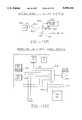
- FIG. 2is a schematic diagram of the programmable gate array as seen by the program data.
- the programmable gate arrayincludes a plurality of distributed memory cells referred to as the configuration memory 200.
- Program data on line 201is loaded into shift register 202 in response to a clock signal on line 203.
- the detect logic 204determines when the shift register is full by reading a preamble from data on 201. When the shift register is full, the detect logic 204 signals across line 205 a frame pointer logic 206 which generates frame pointer signals across lines 207.
- Control logic 208is responsive to the mode inputs to the device on line 209 to control the detect logic 204 across line 210 and the frame pointer during loading of the configuration memory 200.
- the configuration memory 200is organized into a plurality of frames F1-FN.
- the frame pointer F1is activated to load the first frame in the configuration memory.
- the frame pointer for F2is activated, loading the second frame F2, and so on until the entire configuration memory is loaded.
- Control logic 208generates a program done signal on line 210.
- a basic cell 300consists of a data input line 301 coupled to pass transistor 302.
- the gate of the pass transistor 302is coupled to a read or write control signal on line 303.
- the output of the pass transistor 302is coupled to line 304.
- Line 304is coupled to the input of inverter 305 and to the output of inverter 306.
- the output of inverter 305is coupled to line 307 which is coupled back to the input of inverter 306.
- Lines 304 and 307provide Q and Q outputs for configuration control.
- the basic cell 300consists of two CMOS inverters and a pass transistor.
- the pass transistoris used for writing and reading cell data.
- the cellis only written during configuration and only read during read-back in the programming mode. During normal operation, the pass transistor is off and does not affect the stability of the cell.
- the memory cell outputs Q and Quse full ground and V CC levels and provide continuous direct control.
- the configuration storecan also be implemented with other types of volatile or non-volatile storage cells.
- non-volatile memorylike EPROM, E 2 PROM, programmable resistive links, or Ferro RAM, could be used.
- the device memoryis configured as mentioned above by downloading a bit stream from a host system or an external memory, such as an EPROM.
- the configuration processesare the same as those used in prior art programmable gate array, with one exception which is discussed below with reference to the configurable logic blocks.
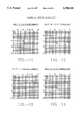
- FIG. 4illustrates the notation used for the vertical buses.
- Each vertical bushas 25 lines.
- Lines 1-4 and 15-17are long lines which run across the entire array.
- Lines 5-14consist of bidirectional general interconnect segments which are coupled through switching matrices and segment boxes as described below.
- Lines 18-25are uncommitted long lines which run the entire length of the array.
- FIG. 5illustrates the notation used for the horizontal buses.
- Each horizontal busis a 23 line bus in which lines 1-4 and 15 are long lines, lines 5-14 are bidirectional general interconnect segments, and lines 16-23 are uncommitted long lines.
- lines 1-4 and 15are long lines
- lines 5-14are bidirectional general interconnect segments
- lines 16-23are uncommitted long lines.
- the distinctions between the long lines, the bidirectional general interconnect segments, and the uncommitted long linesare set out in detail below.
- the horizontal and vertical busesrequire means of interconnection. This occurs at the intersections of the horizontal buses and the vertical buses.
- the interconnections between the lines at the intersectionare made through programmable interconnect points, switch matrices, and segment boxes.
- FIG. 6illustrates the placement of the switch matrices in the interconnect structure.
- the switch matricesare positioned at the intersections of vertical bus 2-8 with horizontal buses 2-8.
- FIG. 6illustrates the placement of the switch matrices on horizontal bus 4 adjacent the configurable logic block R3C3, R3C4, R4C3, and R4C4. It can be seen that the switch matrices are positioned only on lines 5-14 of the bidirectional general interconnect structure.
- the bidirectional general interconnect structureconsists of segments which are two configurable logic blocks in length, spanning, in this case, from switch matrix 600, located on vertical bus 3, to switch matrix 601, located on vertical bus 5 in lines 5-9 of a bidirectional general interconnect.
- Switch matrix 602is coupled to segments of line 10-14 which extend from vertical bus 2 to vertical bus 4 and vertical bus 4 to vertical bus 6. Vertical buses 2 and 6 are not shown in FIG. 6.
- a connection to a bidirectional general interconnectallows propagation of the signal across a width equal to two configurable logic blocks on the array without passing through a switch matrix. This allows networks with fewer delays due to switch matrices.
- FIGS. 7 and 8illustrate the complete intersection between vertical buses 2-8 and horizontal buses 2-8, where a circle indicates a bidirectional programmable interconnect point controlled by a memory cell in the configuration memory.
- FIG. 7is the structure for the intersection of odd numbered vertical buses with odd numbered horizontal buses, and even numbered vertical buses with even numbered horizontal buses.
- FIG. 8is the structure for the even-odd and odd-even intersections between vertical and horizontal buses.
- horizontal line 1is connectable to vertical lines 1 and 4.
- Horizontal line 2is connectable to vertical lines 2 and 3.
- Horizontal line 3is connectable to vertical lines 2 and 3.
- Horizontal line 4is connectable to vertical lines 1 and 4.
- Horizontal lines 5-9are coupled to the left side 700 of a switch matrix.
- the right side 701 of the switch matrixprovides line 5 which is connectable to vertical line 14.
- the horizontal line 6 output from the right side 701 of the switch matrixis connectable to vertical line 13.
- Horizontal line 7 from the switch matrixis coupled through a programmable interconnection point (PIP) to vertical line 12.
- Horizontal line 8 from the switch matrix side 701is coupled through PIP to vertical line 11.
- Horizontal line 9 output from the right side 701 of the switch matrixis coupled through a PIP to vertical line 10.
- the bidirectional general interconnect segments 10-14 of the horizontal busare connectable through PIPs to the bidirectional general interconnect segments in the vertical bus lines 5-9 and 10-14 in the configuration shown.
- Lines 10-13 of the horizontal bus bidirectional segmentsare connectable to the odd numbered uncommitted long lines 19, 21, 23 and 25 through PIPs as shown.
- the horizontal long line 15passes through the intersection without being connectable to any other line.
- the odd numbered uncommitted long lines 17, 19, 21, and 23 in the horizontal busare connectable through PIPs to the vertical bidirectional interconnect segments 10-13 as shown.
- FIG. 8The interconnection of the even or odd numbered vertical buses with odd or even numbered horizontal buses, respectively, is shown in FIG. 8. As with the intersection shown in FIG. 7, the horizontal lines in the intersection structure of FIG. 8 are connectable through PIPs and the switch matrix to the vertical lines.
- Horizontal long line 1is connectable to vertical lines 1 and 4.
- Horizontal long line 2is connectable to vertical lines 2 and 3.
- Horizontal long line 3is connectable to vertical long lines 2 and 3.
- Horizontal long line 4is connectable to vertical long lines 1 and 4.
- Horizontal bidirectional general interconnects 5-9are connectable to the bidirectional general interconnects 5-14 as shown in the figure and to the even numbered uncommitted long lines 18, 20, 22, and 24.
- the bidirectional general interconnects 10-14are connectable to the vertical bidirectional general interconnects 5-9 and through the switching matrix to the adjacent segments of lines 10-14 in both the vertical and the horizontal buses.
- the even numbered uncommitted long lines 16, 18, 20, and 22 on the horizontal busare connectable to the vertical bidirectional segments 6-9 as shown.
- FIG. 9illustrates the intersection of horizontal buses 1 and 9 with the even numbered vertical buses 2-8 and vertical buses 1 and 9.
- FIG. 10illustrates the intersection of the horizontal buses 1 and 9 with the odd numbered vertical buses 3-7.
- the horizontal long lines 1-4are connectable to vertical long lines 1-4 as shown.
- the bidirectional general interconnect lines 5-9are connectable through the segment box to vertical interconnects 5-9.
- the bidirectional general interconnects 10-14are connectable to vertical bidirectional general interconnects 10-14.
- the bidirectional general interconnects 10-13are connectable to the odd numbered uncommitted long lines 19, 21, 23, and 25.
- the odd numbered uncommitted long lines 17, 19, 21, and 23 on the horizontal busare connectable to the bidirectional general interconnect segments 10-13 as shown.
- long lanes 1-4 on the horizontal busare connectable respectively to vertical lines 1-4.
- the bidirectional general interconnect segments 5-9are connectable to the vertical segments 5-9 and to the even numbered uncommitted long lines 18, 20, 22, and 24 as shown.
- the horizontal bidirectional general interconnect segments 10-14are connected to the segment box in both the horizontal and vertical directions.
- the even numbered uncommitted long lines 16, 18, 20, and 22 on the horizontal busare connectable to vertical bidirectional general interconnect segments 6-9 as shown.
- FIG. 11illustrates the intersection of horizontal bus 1 with vertical bus 1.
- the lines 1-14 in the horizontal busare connectable respectively to lines 1-14 in the vertical bus.
- the even numbered uncommitted long lines 18, 20, 22, and 24 on the vertical busare connectable to horizontal bidirectional general interconnect segments 6-9.
- the even numbered uncommitted long lines 16, 18, 20, and 22 on the horizontal busare connectable to the vertical lines 6-9,
- FIG. 12illustrates the intersection of horizontal bus 1 with vertical bus 9.
- the horizontal line 1is connectable to vertical lines and 4.
- Horizontal line 2is connectable to vertical lines 2 and 3.
- Horizontal lines 3-14are connectable respectively to vertical lines 3-14.
- the even numbered uncommitted long lines 18, 20, 22, and 24 on the vertical busare connectable to horizontal lines 6-9.
- the even numbered uncommitted long lines 16, 18, 20, and 22 on the horizontal busare connectable to the vertical lines 6-9.
- FIG. 13illustrates the intersection of horizontal bus 9 with vertical bus 1.
- the horizontal lines 1-14are connectable to the vertical lines 1-14, respectively.
- horizontal line 3is connectable to vertical line 2 and
- horizontal line 4is connectable to vertical line 1.
- the horizontal lines 6-9are also connectable to the even numbered uncommitted long lines 18, 20, 22 and 24 on the vertical bus.
- the even numbered uncommitted long lines 16, 18, 20 and 22 on the horizontal busare connectable to vertical lines 6-9.
- FIG. 14illustrates the intersection of horizontal bus 9 with vertical bus 9.
- Horizontal lines 1-14are connectable to vertical lines 1-14, respectively.
- Horizontal lines 6-9are also connectable to the even numbered uncommitted long lines 18, 20, 22 and 24 on the vertical bus.
- the even numbered uncommitted long lines 16, 18, 20 and 22 on the horizontal busare connectable to vertical lanes 6-9.
- FIG. 14Ashows a corner connection that can be used at the intersections of horizontal bus 1 and vertical bus 1, horizontal bus 1 and vertical bus 9, horizontal bus 9 and vertical bus 9, and horizontal bus 9 and vertical bus 1. It has the advantage that it is a single layout that can be used at all four corners while accomplishing the ability to route signals from the long lines 1-4 completely around the perimeter of the chip.
- horizontal lines 1-14are connectable to vertical lines 1-14, respectively.
- Horizontal line 1is connectable to vertical line 4
- horizontal line 2is connectable to vertical line 3
- horizontal line 3is connectable to vertical line 2
- horizontal line 4is connectable to vertical line 1.
- horizontal line 14is connectable to vertical line 5
- horizontal line 13is connectable to vertical line 6
- horizontal line 12is connectable to vertical line 7
- horizontal line 11is connectable to vertical line 8
- horizontal line 10is connectable to vertical line 9
- horizontal line 9is connectable to vertical line 10
- horizontal line 8is connectable to vertical line 11
- horizontal line 7is connectable to vertical line 12
- horizontal line 6is connectable to vertical 13
- horizontal line 5is connectable to vertical line 14.
- horizontal lines 6-9are connectable to the even numbered, uncommitted long lines 18, 20, 22, and 24 on the vertical bus. The even numbered long lines 16, 18, 20, 22 on the horizontal bus are connectable to vertical lines 6-9.
- FIG. 15illustrates the connection of the global clock and global reset signals on vertical lines 16 and 17.
- the global clock signalis supplied from an input buffer 1500 to line 1501.
- Line 1501is directly connected to line 16 in all vertical buses.
- the global reset signalis supplied at global reset buffer 1502.
- the output of the global reset bufferis supplied on line 1503 to line 17 on all the vertical buses.
- the lines 16 and 17 of the vertical busesare directly connected to the input/output blocks as schematically illustrated in FIG. 15 and to each of the configurable logic blocks.
- the direct connections to the configurable logic blocksare shown only to a few of the blocks in the upper left hand corner of the array for clarity of the figure
- FIG. 15Ashows the connection of lines 16 and 17 of the vertical buses to the configurable logic blocks.
- lines 16 and 17are connected only to the input/output blocks as shown.
- FIG. 15Bshows the configurable path from an input/output pad to an IOB or to the global or alternate buffers. It can be seen that the pad 1510 is connected across line 1511 through buffer 1512 to line 1513. Line 1513 is passed through pass transistor 1514 to an IOB input path 1515 or through pass transistor 1516 to the buffer input circuitry on line 1517. A memory cell 1518 in the configuration store controls which pass transistor (1514 or 1516) is enabled.
- FIG. 15Cillustrates the input circuitry to the global clock buffer.
- Input I of IOB 2 and 9are connected to provide a signal on lines 1518 and 1519 as inputs to 8 to 1 multiplexer 1521.
- a clock input pin at IOB 110is connected to line 1520 as illustrated in FIG. 15B as input to multiplexer 1521.
- Lines 14 and 15 in vertical bus 1 and lines 14 and 15 in horizontal bus 1are also coupled as inputs to configurable multiplexer 1521.
- the direct connect output X4 on the configurable logic block in row 1, column 1is directly connected as well as an input to the multiplexer 1521.
- the direct link from an adjacent CLB to the multiplexer 1521 across line 1524provides added flexibility for the generation of the global clock on chip.
- the configuration storecontrols the multiplexer 1521 to supply a clock signal on line 1522 to the global clock buffer 1523.
- FIG. 16illustrates the connection of line 15 in the vertical and horizontal buses. It is designed to perform the function of a local clock for an input/output block or a configurable logic block or as a clock enable signal.
- the line 15 in horizontal busesis connectable to a variety of sources including outputs from configurable logic blocks and the alternate buffers.
- the line 15 in the horizontal busesare connectable to the horizontal alternate buffer 1600 which generates the signal on line 1601.
- a bidirectional buffersuch as buffer 1602.
- Each bidirectional bufferincludes a configurable tristate buffer connected from line 1601 to line 15 in the respective horizontal bus.
- a configurable tristate buffer connected from line 15 on the respective horizontal bussupplies an output to line 1601.
- the configurable tristate buffersare each controlled by a memory cell in the configuration memory.
- the vertical alternate buffer 1603generates a signal on line 1604.
- Line 15 on each vertical bufferis connected to a bidirectional buffer, e.g. buffer 1605.
- Each bidirectional bufferhas a first tristate buffer connected from line 1604 to line 15 in the respective vertical bus and a tristate buffer connected from line 15 in the respective vertical bus to line 1605.
- Each of the tristate buffersis controllable from a storage cell in the configuration memory.
- the line 15's in vertical buses 1 and 9are connected respectively to the input/output blocks on the left side and right side of the chip.
- the line 15's in horizontal buses 1 and 9are connected to the input/output blocks on the top and bottom of the chip as shown.
- FIG. 16Ashows the connection of the input/output blocks to line 15 and the connection of the configurable logic blocks to line 15.
- Each complex IOB 1606has a K input directly connected to line 15 on its adjacent vertical or horizontal bus.
- Each simple IOB 1607is capable of supplying an input signal to line 15 of a horizontal and vertical bus through a PIP.
- Each configurable logic block as shown in FIG. 16Ahas inputs labeled K1, K2, K3 and K4.
- the input K1is connected to line 15 in the horizontal bus above the block.
- Input K2is directly connected to line 15 in the vertical bus to the right of the block.
- Input K3is directly connected to line 15 in the horizontal bus below the block.
- Input K4is directly connected to the vertical bus to the left of the block.
- each configurable logic blockhas output Y1, Y2, Y3 and Y4.
- the output Y1is connectable through a PIP to line 15 in the horizontal bus above the block.
- Output Y2is connectable through a PIP to line 15 In the vertical bus to the right of the block.
- Output Y3is connectable through a PIP to line 15 in the horizontal bus below the block.
- Output Y4is connectable through a PIP to line 15 in the vertical bus to the left of the block.
- the line 1604 connected to the vertical alternate buffer and the line 1601 connected to the horizontal alternate buffercan receive inputs from a number of sources including device pins, and interconnects via PIPs.
- the signal on line 1601can be supplied to all configurable logic blocks and input/output blocks adjacent the horizontal buses with the exception of input/output blocks on the left side and right side of the chip.
- the signal on line 1604can be globally supplied across the chip, with the exception that it cannot be directly connected to the input/output blocks on the top and bottom of the chip.
- a signalcan be generated in configurable logic block R1C1, supplied to line 15 of vertical bus 2 through the bidirectional buffer 1608 to line 1604. From line 1604, it can be supplied anywhere in the chip. A similar net can be formed along horizontal buses.
- This line 15 structureallows the registers in any configurable logic block to receive a clock from one of five sources.
- the sourcesinclude the global clock GK supplied on vertical bus line 16, and the local clocks K1, K2, K3, and K4 which are connected to line 15 on four adjacent interconnect buses.
- the registers in a complex input/output blockcan receive a clock from two sources.
- the first sourceis line 16 in the adjacent vertical bus at its GK input and from an input K on the configurable I/O block connectable through a PIP to line 15 on either a horizontal or vertical bus depending on the location of the input/output block.
- Each line 15 in either a horizontal or a vertical buscan carry a signal obtained from one of four sources.
- the four sourcesinclude an alternate buffer, an adjacent configurable logic block, an adjacent input/output block, and a configurable logic block which has supplied a signal to line 15 of a different bus which has in turn been connected through the bidirectional buffers to levels 1601 or 1604.
- the long lines connecting to that buffercan either be independent where the bidirectional buffers are configured to supply a high impedance state to the long line, or they can use the alternate buffer as a source.
- FIG. 16Billustrates the input structure to the vertical alternate buffer 1603.
- the input to the vertical alternate buffer 1603is provided on line 1610 at the output of the configurable multiplexer 1611.
- the signal on line 1610is connected for supply as output signals at IOB 1612 and at IOB 1613.
- Inputs to the multiplexer 1611include an oscillator signal OSC as generated by the circuitry illustrated in FIGS. 16D and 16E.
- an input signal from IOB 1612is an alternative input to multiplexer 1611 across line 1614.
- a vertical clock input signalis supplied on line 1615 as input to multiplexer 1611 from IOB 1616 configured as shown in FIG. 15B.
- Long lines 5 and 15 of the vertical bus 9 and long lines 5 and 15 of the horizontal bus 9are also connected as inputs to multiplexer 1611.
- the final input to multiplexer 1611is a direct link from output X2 of the configurable logic block in row 8, column 8, across line 1617.
- the vertical alternate buffer 1603also includes a memory cell 1618 for tristate control.
- FIG. 16Cillustrates the input structure for the horizontal alternate buffer 1600.
- the horizontal alternate bufferis tristatable in response to the signal at memory cell 1620.
- the input to horizontal alternate buffer 1600is supplied on line 1621 at the output of the configurable multiplexer 1622.
- Inputs to the configurable multiplexer 1622include the horizontal clock input signal on line 1623, and input signals on lines 1624 and 1625 from input/output structures 1626 and 1627, respectively.
- the vertical bus lines 5 and 15 and horizontal bus lines 5 and 15are connectable as inputs as well to the multiplexer 1622.
- a direct link from the configurable logic block in row 8, column 1, output X4is coupled across line 1628 as an input to multiplexer 1622.
- the on chip oscillator which supplies the OSC signal as one input to the multiplexer 1611 driving the vertical alternate buffer 1603is shown in FIG. 16D.
- the OSC signalis provided at the output of multiplexer 1630 which is controlled by memory cell 1631.
- Inputs to multiplexer 1630include the signal on line 1632 which is supplied at the output of inverting buffer 1633.
- the input to inverting buffer 1633is the signal on line 1634 which is supplied at the output of the oscillator amplifier 1635.
- the input to the oscillator amplifier 1635is supplied at IOB 1636.
- IOB 1637is coupled directly to line 1634.
- Line 1634is supplied through inverting buffer 1638 as a clock input on line 1639 to register 1640.
- Register 1640is connected as a divide-by-two circuit by coupling line coupled from its Q output through inverting buffer 1642 as the D input to register 1640.
- the Q output of register 1640is supplied on line 1643 as a second input to multiplexer 1630.
- Pad 1637is coupled to line 1650 and pad 1636 is coupled to line 1651.
- Resistor R1is connected between line 1650 and 1651.
- Line 1651is coupled through capacitor C1 to GROUND and through crystal 1652 to line 1653.
- Line 1653is coupled through capacitor C2 to GROUND and through resistor R2 to line 1650.
- the divide-by-two option in the oscillator circuitis provided to ensure symmetry of the signal.
- the output of the 2:1 multiplexer 1630gives this choice, and is set during device configuration.
- the paths 1637 and 1636are configurable as shown in FIG. 15B to behave as standard IOBs.
- the oscillator circuitbecomes active before configuration is complete to allow it to stabilize.
- FIG. 17The structure of the programmable interconnect points (PIPs) is shown in FIG. 17 and an alternative structure is shown in FIG. 18.
- the structure in FIG. 17illustrates that for an intersecting conductive segment, such as long lines 1700 and 1701, with long line 1702, a PIP is implemented using a pass transistor.
- pass transistor 1703provides for interconnection between lines 1702 and 1701.
- Pass transistor 1704provides for interconnection between lines 1700 and 1702.
- the memory cell 1705 from the configuration storecontrols the pass transistor 1703 to provide a bidirectional path between the lines.
- memory cell 1706controls pass transistor 1704 to provide the bidirectional path.
- FIG. 17illustrates that a PIP can be implemented as a multi-source multiplexer 1800.
- Multiplexer 1800can have three sources, source 1, source 2, and source 3, and select a destination line 1801 in response to memory cells 1802 in the configuration store.
- two memory cellscan provide for selection from among three or four sources.
- the equivalent symbol for the circuit using multiplexer 1800is shown at 1803. It should be recognized that the multiplexer implementation is a unidirectional interconnect which allows for connection from any one of the source lines to the destination line and not vice versa. Furthermore, only one source line can be activated for a given operation.
- FIG. 19illustrates the implementation of the switch matrix according to the present invention.
- Each switch matrixhas five connections on the top labeled 1-5, five connections on the right side labeled 6-10, five connections on the bottom labeled 11-15, and five connections on the left side labeled 16-20.
- Line 1is connectable through PIP 1-20 to line 20, through PIP 1-6 to line 6, through PIP 1-11 to line 11, and through PIP 1-15 to line 15.
- Line 2is connectable through PIP 2-19 to line 19, PIP 2-7 to line 7, PIP 2-14 to line 14, and PIP 2-15 to line 15.
- Line 3is connectable through PIP 3-18 to line 18, PIP 3-8 to line 8, PIP 3-13 to line 13, and PIP 1-14 to line 14.
- Line 4is connectable through PIP 4-17 to line 17, PIP 4-9 to line 9, PIP 4-12 to line 12, and PIP 4-13 to line 13.
- Line 5is connectable through 5-16 to line 16, PIP 5-10 to line 10, PIP 5-11 to line 11, and PIP 5-12 to line 12.
- connections of lines 6-10include the following.
- Line 6is connectable through PIP 6-15 to lane 15, PIP 6-16 to line 16, and through PIP 6-20 to line 20.
- Line 7is connectable through PIP 7-14 to line 14, and through PIP 7-19 to line 19, and PIP 7-20 to line 20.
- Line 8is connectable through PIP 8-13 to line 13, PIP 8-18 to line 18, and PIP 8-19 to line 19.
- Line 9is connectable through PIP 9-12 to line 12, PIP 9-17 to line 17, and PIP 9-18 to line 18.
- Line 10is connectable through PIP 10-11 to line 11, PIP 10-16 to line 16, and PIP 10-17 to line 17.
- connection of line 20 through PIP 20-15 to line 15the connection of line 19 through PIP 19-14 to line 14, the connection of line 18 through PIP 18-13 to line 13, the connection of line 17 through PIP 17-12 to line 12, and the connection of line 16 through PIP 16-11 to line 11.
- FIG. 20illustrates the repowering buffer which is used with a horizontal segment and a vertical segment for each switching matrix.
- Repowering buffersare used for reshaping a signal after it has passed through a number of PIPs.
- Each repowering bufferadds delay to the net being routed. Thus, for short nets, the designer would want to avoid using the repowering buffers.
- the repowering buffer as shown in FIG. 20is connected on one of the bidirectional general interconnect segments designated line X in the Figure, where X is one of lines 5-14 in a horizontal or vertical bus.
- Line Xenters the left side of the repowering buffer at point 2000.
- Point 2000is supplied as input to a first tristate buffer 2001.
- the output of the tristate buffer 2001is connected to point 2002 which is supplied at the output of the repowering buffer back to line X.
- Point 2002is also supplied at the input of a tristate buffer 2003.
- the output of the tristate buffer 2003is connected at point 2000 for supply of the signal in the right to left direction.
- a third path, through pass transistor 2004,is supplied between points 2000 and 2002.
- the first memory cell M1 and a second memory cell M2control the operation of the repowering buffer.
- the true output of memory cell M1is supplied to AND-gate 2005.
- the complement output of memory cell M2is supplied as a second input to AND-gate 2005.
- the output of AND-gate 2005is the tristate enable input to buffer 2003.
- the inverted output of memory cell M1is supplied at a first input to AND-gate 2006.
- the second input to AND-gate 2006is the inverted output of memory cell 2002.
- the output of AND-gate 2006is the tristate control signal for buffer 2001.
- the true output of memory cell M2is supplied to control the pass transistor 2004.
- the repowering buffer shown in FIG. 20supplies for repowering of a signal propagating in either direction along line X.
- the pass transistor 2004allows for bypassing of the repowering buffer.
- the line location of the repowering buffer for a given switching matrix or segment boxshould be determined as meets the needs of a particular application.
- the repowering buffershould be utilized for current CMOS technology for any network path passing through around four or more PIPs, and not going through a CLB or IOB.
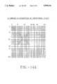
- FIG. 21illustrates the interconnection options for a switch matrix using the PIP array as shown in FIG. 19.
- the figureis a graphical representation showing the possible interconnections of each of the connections 1-20 through the switching matrix.
- the possible interconnections of connection 1is shown in the upper left hand corner.
- the possible interconnections of connection 20are shown in the lower right hand corner.
- FIG. 22illustrates the interconnection array for the segment box on vertical buses 1 and 9. It can be seen that the segment box is an alternative switch matrix design, adapted for the peripheral buses.
- Each segment boxhas 20 input connections, five on each side, as illustrated in the figure.
- the input connections 20 and 6are directly connected, input connections 19 and 7 are connected, inputs 18 and 8 are connected, inputs 17 and 9 are connected, and inputs 16 and 10 are connected.
- Inputs 1 and 15are connectable through PIPs to the line connecting inputs 20 and 6.
- Inputs 2 and 14are connectable through respective PIPs to the line connecting inputs 9 and 7.
- Inputs 3 and 13are connectable through PIPs to the line connecting inputs 18 and 8.
- Inputs 4 and 12are connectable through PIPs to the line connecting inputs 17 and 9.
- inputs 5 and 11are connectable through PIPs to the line connecting inputs 16 and 10.
- the segment box on the horizontal buses 1 and 9is shown in FIG. 23.
- inputs 1 and 15are connected directly
- inputs 2 and 14are connected directly
- inputs 3 and 13are connected directly
- inputs 4 and 12are connected directly
- inputs 5 and 11are connected directly.
- Inputs 20 and 6are connectable through PIPs to the line connecting inputs 1 and 15
- inputs 19 and 7are connectable through PIPs to the line connecting inputs 2 and 14.
- Inputs 18 and 8are connectable through PIPs to the line connecting inputs 3 and 13.
- Inputs 17 and 9are connectable through PIPs to the line connecting inputs 4 and 12.
- inputs 16 and 10are connectable through PIPs to the line connecting inputs 5 and 11.
- FIG. 24graphically illustrates in the style of FIG. 21, the possible interconnections for each input to a segment box. These possible interconnections apply equally to the segment boxes on the vertical buses and to the segment boxes on the horizontal buses.
- FIG. 25A detailed implementation of the configurable logic block is set out with reference to FIGS. 25-44. An overview block diagram is set out in FIG. 25.
- the configurable logic block 2500 shown in FIG. 25consists of a combinational function and control generator 2501 which receives inputs from four sides, schematically illustrated by buses 2502-1, 2502-2, 2502-3, and 2502-4.
- the combinational function and control generator 2501communicates with four independently configurable output ports 2503-1, 2503-2, 2503-3, and 2503-4.
- the output portsreceive signals and supply feedback signals to and from the combinational function and control generator 2501 across respective buses 2504-1, 2504-2, 2504-3, and 2504-4.
- Each output portsupplies a plurality of output signals, schematically illustrated by the respective output buses 2505-1, 2505-2, 2505-3, and 2505-4.
- FIG. 25illustrates at a high level the symmetry of the configurable logic block 2500.
- Input signalscan be received from all four sides of the block, likewise, output signals can be supplied to any of the four sides of the block.
- input signals from the input bus 2502can be used to generate output signals across bus 2505-1, 2505-2, 2505-3, or 2505-4. Similar flexibility is provided from all of the other input buses in the configurable logic block.
- the inputs and outputs to the configurable logic blockare set out in FIG. 26. Also, a notation for the inputs and outputs is provided. It can be seen that input signals along the top side of the bus are labeled A1 through D1, EM1, EN1, FM1, FN1, G1, H1, and K1. The outputs are labelled X1 and Y1. Similarly, the suffix 2 is applied to the right side of the chip, the suffix 3 is applied to the bottom of the chip, and the suffix 4 is applied to the left side of the chip. On the left side of the chip, additional inputs GR and GK for global reset and global clock signals are provided.
- the inputs A1 through A4 and B1 through B4are long line inputs.
- Inputs C1 through C4 and D1 through D4are inputs coupled to the bidirectional general interconnect segments for logic signals.
- the inputs EM1 through EM4, FM1 through FM4, EN1 through EN4, and FN1 through FN4are direct connect inputs.
- the inputs G1 through G4 and H1 through H4are inputs to the bidirectional general interconnect segments for control signals.
- the inputs K1 through K4are long line inputs from bus line 15 used for clock and clock enable functions.
- Outputsare supplied at terminals X1 through X4 and Y1 through Y4.
- Direct connect structuresare connected to X1 through X4.
- the general interconnect structuresare coupled to outputs Y1 through Y4.
- the combinational logic blockconsists of a 64 bit RAM addressed through a multiplexing tree as shown in FIG. 27, 16 additional bits of RAM addressed through a special output multiplexer as shown in FIG. 28, four independent output macro cells as shown in FIGS. 29-32, and multiplexing structures used for generation of the logic inputs to the multiplexing tree and for control signals shown in FIG. 35-44.
- the basic combinational logic functionis provided by the multiplexing tree shown in FIG. 27.
- 64 bits of the configuration memory 2700is stored with program data.
- a first level multiplexing structuredivides the 64 bit RAM into eight 8 bit sections. Each 8 bit section is coupled to a 8:1 multiplexer, 2701-1 through 2701-8.
- the 8 bit multiplexersare coupled into pairs sharing three common address signals VA1, VB1, VC1 for multiplexers 2701-1 and 2701-2, signals VA1, VB2, VC2 for multiplexers 2701-3 and 2701-4, signals VA3, VB3, VC3 for multiplexers 2701-5 and 2701-6, and finally, signals VA4, VB4, and VC4 for multiplexers 2701-7 and 2701-8.
- Eight independent outputsare generated by the eight 8:1 multiplexers.
- the outputs FA1 through FA4are supplied respectively from multiplexers 2701-1, 2701-3, 2701-5 and 2701-7.
- Outputs FB1 through FB4are supplied respectively from multiplexers 2701-2, 2701-4, 2701-6 and 2701-8.
- the paired outputs FA1/FB1are supplied to cross-multiplexer 2702-1.
- FA2/FB2are supplied to cross-multiplexer 2702-2.
- FA3/FB3are supplied to cross-multiplexer 2702-3.
- FA4/FB4are supplied to cross-multiplexer 2702-4.
- the cross-multiplexers 2702-1 through 2702-4are each coupled to a respective memory cell 2703-1 through 2703-4 in the configuration memory to receive a respective control variable VD1 through VD4.
- Cross-multiplexer 2702-1generates outputs FC1 and FD1.
- Cross-multiplexer 2702-2generazes outputs FC2 and FD2.
- Cross-multiplexer 2702-3generates outputs FC3 and FD3.
- Cross-multiplexer 2702-4generates outputs FC4 and FD4.
- cross-multiplexer 2701-1If the memory cell 2703-1 associated with cross-multiplexer 2701-1 is equal to 0, then the input FA1 is connected to output FC1, and the input FB1 is connected to output FD1.
- the control variable VD1 coupled to cross-multiplexer 2702-1will have no effect when memory cell 2703-1 is 0.
- a cross-multiplexerjust provides a pass through path for the signals FA1 and FB1, such that the output FC1 and FD1 are two independent variables of the three control signals VA1 through VC1.
- cross-multiplexers 2702-2 through 2702-4The function of the cross-multiplexers 2702-2 through 2702-4 is identical as to that of 2702-1 with the exception that the control signals VD2 through VD4 are independently supplied from the input multiplexing structure. Also, each memory cell 2703-2 through 2703-4 is individually configured during programming.
- the output signals FC1 and FC2are supplied as inputs to third level multiplexer 2704-1. Likewise, signals FC3 and FC4 are supplied to third level multiplexer 2704-2. Logic signals VE1 and VE2 control multiplexers 2704-1 and 2704-2, respectively. The output FE1 of multiplexer 2704-1 and FE2 of 2704-2 represent a logic function of five variables.
- the signals FE1 and FE2are supplied as input to a fourth level multiplexer 2705.
- Multiplexer 2705is controlled by signal VF and generates the output F in response to six variables.
- the signal Fis supplied to a special output multiplexer 2706.
- a second input to the multiplexer 2706is the special output signal G.
- Multiplexer 2706is controlled in response to independent variable VG and generates the output signal H.
- a special output signal Gis generated by the special output stage shown in FIG. 28.
- the special output stageconsists of 16 bits of RAM 2800 in the configuration memory. The 16 bits are coupled to a 16:1 multiplexer 2801. Control inputs to the 16:1 multiplexer include the signals FD1 through FD4 generated by the cross-multiplexers 2702-1 through 2702-4 in FIG. 27. Because the 16 control signals VA1 through VD1, VA2 through VD2, VA3 through VD3, and VA4 through VD4 can be independently supplied by the input multiplexing structure from outside the CLB, the special output G represents a wide gating function of 16 variables. Thus, a limited function of 16 variables is available at the G output.
- the configurable logic block of the present inventionuses 64 bits cascaded with 16 bits to give the ability to decode 64 states of 16 input variables.
- the output macro cells for the configurable logic blockare shown in FIGS. 29-32.
- the macro cell in FIG. 29is coupled to outputs X1 and Y1 of the configurable logic block.
- Inputs to the macro cellinclude FC1, FE1, H and FD1.
- the inputs FC1, FE1 and Hare coupled to multiplexer 2900.
- the output DQ1 of multiplexer 2900is supplied as a D input to register 2901.
- the output Q1 of register 2901is coupled as an input to multiplexer 2902.
- Two additional inputs to multiplexer 2902include FC1 and FE1.
- the output of multiplexer 2902is coupled to line 2903.
- Line 2903supplies the signal QF1 as feedback to the combinational logic. Likewise, it is coupled directly to an output buffer 2904 for driving the output signal Xi for the direct connect.
- Signal 2903is also coupled to multiplexer 2905.
- the second input to multiplexer 2905is a signal FD1.
- the output TY1 of multiplexer 2905is coupled to a tristate output buffer 2906.
- the output of buffer 2906is the Y1 signal for connection to the interconnect structure.
- the tristate buffer 2906is controlled by the control signal OE1 generated within the configurable logic block as described below.
- the register 2901 in the macro cellfurther has the ability to be preloaded during programming. This functionality is illustrated in FIG. 29A where the signal DQ1 is supplied to a multiplexer 2908.
- the second input to multiplexer 2908is program data.
- the multiplexer 2908is controlled by the control signal PROGRAM DONE. When PROGRAM DONE is false, the program data is selected through to the D input of the register 2901. Otherwise, the signal DQ1 is supplied.
- the register 2901is clocked at the output of gate 2909.
- the gate 2909provides an OR function with the frame pointer and the output of AND-gate 2910.
- the inputs to AND-gate 2910include the clock signal CK generated within the configurable logic block and the inverse of PROGRAM DONE.
- the clock signalis disabled and the frame pointer is used to clock register 2901 with program data. After programming is completed, the clock signal is supplied directly through to the register 2901.
- the same structureis utilized in each of the macro cells, although it is not explicitly shown to clarify the diagrams.
- FIG. 30shows the macro cell supplying the outputs X2 and Y2.
- the inputs to macro cell 2 in FIG. 30include FC2, FE2, H, and FD2.
- FC2, FE2, and Hare supplied through multiplexer 3000 to generate the signal DQ2.
- DQ2is supplied to register 3001.
- the output Q2 of register 3001is supplied as an input to multiplexer 3002.
- Other inputs to multiplexer 3002include FC2 and FE2.
- the output QF2 of multiplexer 3002is supplied on line 3003 as feedback and directly to output buffer 3004 supplying the signal X2 to the direct connect.
- the signal on line 3003is also supplied to multiplexer 3005.
- the second input to multiplexer 3005is the signal FD2.
- the output TY2 of multiplexer 3005is supplied as an input to tristate output buffer 3006, which drives the signal Y2.
- Tristate buffer 3006is controlled by control signal OE2.
- the output macro cell of FIG. 31drives the signals X3 and Y3. Its inputs include the signals FC3, FE1, D1, H and FD3. The inputs FC3, FE1, and D1 are coupled through multiplexer 3100 to supply the signal DQ3. Signal DQ3 is coupled to register 3101. The output Q3 of register 3101 is supplied as an input to multiplexer 3102. Two other inputs to multiplexer 3102 include FC3 and H. The output QF3 of multiplexer 3102 is supplied on line 3103 as feedback and directly to the buffer 3104 which drives the signal X3. Also, the signal on line 3103 is supplied to multiplexer 3105. The second input to multiplexer 3105 is signal FD3. The output TY3 of multiplexer 3105 is supplied to the tristate buffer 3106 driving the signal Y3. The tristate buffer 3106 is controlled by the signal OE3.
- the output macro cell for the driving signals X4 and Y4is shown in FIG. 32. It is similar to the macro cell of FIG. 31.
- the input signalsinclude FC4, FE2, D2, H, and FD4.
- the signals FC4, FE2 and D2are supplied through multiplexer 3200 to supply the signal DQ4.
- Signal DQ4is supplied through register 3101 to generate the output signal Q4.
- the output signal Q4is supplied to multiplexer 3102.
- Other inputs to multiplexer 3102include FC4 and H.
- the output of multiplexer 3102is the signal QF4 on line 3203 which is supplied as feedback and is coupled to buffer 3204 to drive the signal X4.
- the signal on line 3203is also supplied to multiplexer 3205.
- a second input to multiplexer 3205is the signal FD4.
- Multiplexer 3205generates a signal TY4 which is coupled to the tristate buffer 3206.
- Tristate buffer 3206is controlled by the signal OE4 and drives the output Y4 of the
- a design goal of the macro cellsis to provide symmetrical function of each of the macro cells. Accordingly, to provide greater symmetry, the macro cell 1 and macro cell 2 could be changed to allow for the addition of input signals D3 and D4, respectively, at the input multiplexers 2900 and 3000. Further, the ability to provide the signal H in either a registered or combinatorial function could be allowed at each of the macro cells. The same is true for the signals FE1 and FE2. However, to optimize utilization of the die in the preferred embodiment, the macro cells shown in FIGS. 29-32 have been adopted. Complete symmetry would be attained by replacing the 3:1 muxes with 4:2 muxes in FIGS. 29-32.
- the macro cells of FIGS. 31 and 32provide for utilization of the registers 3101 and 3201 even if they are not used for driving the output of the combinational logic. This is provided by allowing the inputs D1 and D2 to be directly coupled to the registers in the output macro cells.
- each registerincludes a clock, clock enable and reset control.
- each of the multiplexers shown in the figuresunless a dynamic control signal is explicitly shown, is controlled by memory cells in the configuration program.
- the configuration of the macro cellsis set during programming of the device. Note that each of the macro cells receives signals from the second level of multiplexing, the third level of multiplexing, and the output signal H.
- the macro cellallows the output X1 and the output Y1 to be driven from different sources at the same time. This gives the configurable logic block the ability to produce up to eight outputs at a time.
- the Y1 through Y4 signalsare each applied to drive eight bus lines in the interconnect through PIPs, one of which is an uncommitted long line.
- the outputs X1 through X4provide a high speed signal path to adjacent and next adjacent configurable logic cells or input/output cells in the array.
- the input multiplexing for the configurable logic block for generation of the signals VA1 through VA4is shown in FIG. 33.
- the structureincludes the first 4:1 multiplexer 3300 receiving the signals A1, A2, FD2, and QF2 as inputs.
- the output of multiplexer 3300is supplied as an input to 3:1 multiplexer 3301.
- Two additional inputs to multiplexer 3301include FM2 and FN2.
- the output of multiplexer 3301is the signal DA3 on line 3302.
- Other inputs to the multiplexing treeinclude the signals C1 and QF1 supplied to the 2:1 multiplexer 3303.
- the output of the 2:1 multiplexer 3303is the signal DA1 on line 3304.
- the inputs C1 and QF1are also supplied to a second input multiplexer 3310 which supplies the output DA2 on line 3311.
- the input signals EM1 and EN1are supplied to 2:1 multiplexer 3305.
- the output E1is supplied on line 3306.
- the input D1is coupled to line 3307.
- the signal VA1is supplied at the output of 4:1 multiplexer 3308.
- the four inputs to multiplexer 3308include the signals D1, El, DA1, and DA3.
- the signal VA2is supplied at the output of multiplexer 3309.
- the inputs to multiplexer 3309include the signals D1, El, DA1 and DA3.
- the signal VA3is supplied at the output of multiplexer 3312.
- the inputs to multiplexer 3312include D1, El, DA2 and DA3.
- the signal VA4is supplied at the output of 4:1 multiplexer 3313.
- the inputs to multiplexer 3313include D1, El, DA2 and DA3. All of the multiplexers shown in FIG. 33 are controlled by memory cells in the configuration memory.
- the control signals VB1 through VB4are generated in the multiplexing tree which is identical to the MUX tree of FIG. 33, except that the inputs are different. Thus, the connection of the multiplexing tree is not repeated here. Rather, only the inputs are recited.
- the inputs to the multiplexing treeinclude FN3, FM3, A3, A4, FD3, QF3, C2, QF2, EM2, EN2, and D2. Accordingly, any one of the control signals generated by the multiplexing tree in FIG. 34 is selected from one of eleven inputs.
- FIGS. 35 and 36show respectively the multiplexing trees generating the control signals VCI through VC4, and VD1 through VD4.
- the inputs to the multiplexing tree in FIG. 35include FN4, FM4, B1, B2, FD4, QF4, C3, QF3, EM3, EN3 and D3.
- the inputs to the multiplexing tree of FIG. 36include FN1, FM1, B3, B4, FD1, QF1, C4, QF4, EM4, EN4 and D4.
- control signals VA1 through VA4, VB1 through VB4, VC1 through VC4, VC1 through VD4,are generated using an input multiplexing tree which does not require sharing of input variables.
- each of the outputscan be derived from an independent input variable allowing for a function of from 1 to 16 independent variables.
- the inputsare derived from all four sides of the configurable logic block allowing for symmetrical implementation of a network on the array.
- FIGS. 37, 38, and 39illustrate generation of the control signals VE1, VE2, VF and VG.
- the MUX treegenerates the signals VE1 and VE2 in response to the control signals CT1 and CT2 and to the input signals C1 and C3.
- VE1is generated at the output of multiplexer 3700 which receives all four of the input variables CT1, CT2, C1, C3 as inputs.
- the signal VE2is generated the output of 4:1 multiplexer 3701 which receives CT2, CT1, C1 and C3 as inputs.
- control signals CT1 and CT2 of FIG. 37 and CT3, CT4 and CT5are generated in FIGS. 40A-40E described below.
- the signal VFis generated at the output of multiplexer 3800 shown in FIG. 38.
- Multiplexer 3800is a 4:1 multiplexer receiving the inputs CT3, CT4, C2 and C4.
- the signal VGis generated at the output of the 3:1 multiplexer 3900 shown in FIG. 39, receiving the input signals CT5, V CC and GROUND.
- FIGS. 40A-40Hillustrate generation of the internal control signals CT1 through CT8, respectively.
- FIG. 40Aillustrates generation of the signal CT1 in response to the inputs G1 and G2 through multiplexer 4001.
- FIG. 40Billustrates generation of the signal CT2 through multiplexer 4002 in response to inputs G3 and G4.
- FIG. 40Cillustrates generation of the signal CT3 through multiplexer 4003 in response to inputs H1 and H2.
- FIG. 40Dillustrates generation of the signal CT4 through multiplexer 4004 in response to inputs H3 and H4.
- FIG. 40Eillustrates generation of the signal CT5 by multiplexer 4005 in response to inputs G1 and G2.
- FIG. 40Fillustrates generation of the signal CT6 by multiplexer 4006 in response to inputs G3 and G4.
- FIG. 40Gillustrates generation of the signal CT7 by multiplexer 4007 in response to inputs H1 and H2.
- FIG. 40Hillustrates generation of the signal CT8 by multiplexer 4008 in response to inputs H3 and H4.
- FIG. 41illustrates generation of the output enable signals OE1 through OE4 used in the output macro cells of FIGS. 29-32.
- Each of the signals OE1 through OE4is independently supplied by respective multiplexers 4100, 4101, 4102 and 4103.
- the inputs to multiplexers 4100, 4101, 4102 and 4103include V CC and the common OE control signal on line 4104.
- the signal on line 4104is generated at the output of 4:1 multiplexer 4105.
- 4:1 multiplexer 4105is coupled to four memory cells in the configuration memory 4106.
- Multiplexer 4105is controlled by the signals CT5 and CT6.
- each output enable signalcan be configured to be statically enabled by selecting this V CC as the output signal. Alternatively, it can be dynamically enabled or disabled in response to the common OE control signal on line 4104. Further independence of programming can be accomplished by providing independent dynamic signals for use as the output enables.
- FIG. 42illustrates generation of the clock signal CK which is used to clock the registers in the output macro cells. This signal is generated at the output of 2:1 multiplexer 4200.
- the inputs to the 2:1 multiplexer 4200include a true and complement version of the signal supplied on line 4201 at the output of 6:1 multiplexer 4202.
- Multiplexer 4202receives as inputs the signals K1 through K4 from bus line 15 on four sides of the macro cell, the input GK from the global clock lines, and the control signal CT7.
- the multiplexers in FIG. 42are configured by memory cells in the configuration memory.
- FIG. 43illustrates generation of the clock enable signal which is coupled to the registers in the output macro cells.
- the clock enable signalis generated at the output of multiplexer 4300.
- the input to multiplexer 4300includes a signal on line 4301 which is supplied at the output of the 3:1 multiplexer 4302.
- the second input to multiplexer 4300is the V CC signal.
- the clock enable signalcan be permanently enabled by connection to V CC .
- the inputs to multiplexer 4302include the K1 signal, K2 signal and the control signal CT7.
- FIG. 44illustrates generation of the reset signal RST which is supplied to the registers in the output macro cells in the configurable logic block.
- the reset signalis generated at the output of OR-gate 4400.
- the inputs to OR-gate 4400include the signal on line 4401 which is generated at the output of multiplexer 4402.
- the other input to OR-gate 4400is the global reset signal GR.
- the two inputs to multiplexer 4402include CT8 and GROUND.
- the reset signal CT8can be permanently inhibited by connection to GROUND. Global reset is always allowed.
- the configurable logic block described aboveprovides for symmetrical interfaces on all four sides of the block to the interconnect structure. Furthermore, it allows for wide gating and narrow gating functions without suffering a speed penalty for the narrow gated functions. Furthermore, the wide gating functions do not require sharing of input signals which complicates logic design using the configurable logic block.
- the configurable input/output blocks in the programmable gate array of the present inventionconsist of a simple block as shown in FIG. 45 and a complex block as shown in FIG. 46.
- Each input/output block (IOB)is coupled to memory cells in the configuration memory, the states of which control the configuration of the IOB.
- an IOBallows data to pass in two directions: (i) from an input/output pad to the programmable general connect and specific CLBs; (ii) from the programmable general connect and specific CLBs to a pad.
- the configuration of an IOBsets the type of conditioning the signal receives on passing through the IOB.
- the padmay or may not be bonded to a physical package pin.
- IOBsthere are two types in IOBs in the device.
- a complex IOB as shown in FIG. 46provides an input register/latch and an output register in addition to combinatorial features.
- the complex IOBalso has internal links for giving the user input register read-back at the package pin, and direct links to adjacent complex IOBs that allow data to be transferred to the registers of an adjacent IOB.
- the silicon diecan be put into packages having more than, less than, or the same number of package pins as there are IOB pads on the die. If there are fewer package pins than IOB pads, then some IOBs may not be linked to a device package pins and so become buried IOBs for internal device use.
- the number of simple IOBs and complex IOBs on a given implementationmay vary due to die size and speed constraints.
- the PGAcould include all simple IOBs or all complex IOBs, if desired.
- FIG. 45illustrates the preferred implementation of the simple IOB.
- the IOBprovides a configurable interconnection between the input/output pad 4500 and the interconnect structure.
- the interconnect structuresupplies output signals as inputs to multiplexer 4501.
- the IOBsupplies input signals I to an interconnect bus at the output on line 4503 of buffer 4502.
- Input signals DIare coupled to adjacent configurable logic blocks at the output on line 4505 of buffer 4504.
- Each IOBhas at least one input supplied from a long line on a bus which is perpendicular to the side of the chip on which the IOB is placed. Also, it is connected to the bidirectional general interconnect lines on the bus that runs parallel to the side and to an uncommitted long line on the bus parallel to the side.
- the IOBalso has two direct connect inputs.
- the output of multiplexer 4501is supplied to tristate buffer 4506.
- the tristate buffer 4506has a slew rate control circuit 4507 as known in the art.
- the buffer 4506is controlled by the tristate output signal TO on line 4508.
- the tristate output signal TOis supplied at the output of multiplexer 4509.
- the inputs to multiplexer 4509are the power supply V CC , the true and complement versions of the signal OEN which is supplied as a control input to the IOB from the interconnect structure, and GROUND.
- the pin output signal 70is supplied across line 4510 to the output pad 4500. Coupled to line 4510 also is a passive pull up circuit 4511 which is configured in response to program data through transistor 4512. A pull up resistor 4513 is coupled from the output of transistor 4512 to V CC .
- Inputs from the IO pad 4500are supplied through buffer 4514.
- the output PI of buffer 4514is supplied on line 4515 as input to output buffer 4504 and to output buffer 4502.
- the output buffer 4502is a tristate buffer controlled by the tristate input signal TI on line 4516.
- the tristate input signal TI on line 4516is generated at the output of multiplexer 4517.
- the inputs to multiplexer 4517are V CC , the true and complement of the control signal IEN which is supplied as input to the IO block, and GROUND.
- the multiplexers 4501, 4509, and 4517are each controlled by memory cells in the configuration memory.
- the signal supplied as input to buffer 4514can be derived from three sources: the package pin coupled to the IO pad, the output PO of the output buffer on line 4510, or the high level created by the passive pull up circuit.
- the multiplexer 4517generates the TI signal from four sources.
- V CCWhen V CC is selected, the buffer 4502 is permanently enabled.
- GROUNDWhen GROUND is selected, the buffer 4502 is permanently disabled and does not switch during operation of the programmable gate array, which could cause wasted current drain.
- the multiplexer 4517is configured to select the IEN signal in either its true or complement form, the buffer 4502 is dynamically controlled.
- the multiplexer 4501has six inputs in the preferred system. Two of the inputs come from nearby configurable logic blocks as direct connects, the remaining come from the programmable general interconnect structure.
- the output enable TO on line 4508comes from V CC , OEN or GROUND.
- V CCWhen V CC is selected, buffer 4506 is permanently enabled.
- GROUNDWhen GROUND is selected, buffer 4506 is permanently disabled.
- OENWhen OEN is selected, in either its true or complement forms, buffer 4506 is dynamically controlled.
- the passive pull up 4511 for the output link 4510is controlled by memory cell 4511. When enabled, it ensures that the pad or package pin does not float when it is not used in an application.
- FIG. 46illustrates the complex IOB.
- the complex IOBprovides configurable data paths from the IO pad 4600 to the interconnect across lines 4601 and 4602, and from the interconnect which is coupled to the input multiplexer 4603 to the IO pad 4600.
- the IOBis coupled to the previous counterclockwise adjacent complex IOB to receive input signals QP1 and QP2 at lines 4604 and 4605.
- the IOBsupplies as output the signals Q1 and Q2 to the next clockwise adjacent complex IOB on lines 4606 and 4607.
- the input pathincludes line 4608 which is connected from the IO pad 4600 as input to the input buffer 4609.
- the input bufferdrives a signal PI on line 4610.
- the signal PIis coupled as an input to multiplexer 4611.
- the second input to multiplexer 4611is the output 4612 of multiplexer 4613.
- the inputs to multiplexer 4613include the signals QP1 and QP2.
- Multiplexer 4611is controlled in response to the signal SL1 to supply the signal D1 on line 4614.
- Signal D1is supplied at the data input of the input register/latch 4615.
- the register/latch 4615is clocked by the output 4616 of multiplexer 4617.
- Inputs to multiplexer 4617include the control signals GK, K, and CEN which are supplied as inputs to the IOB.
- the register/latchfurther includes a global reset input 4618 which receives the GR signal, which is an input to the IOB.
- a clock enable input signal LH1is supplied on line 4619 to the register/latch 4615. This signal LH1 is supplied at the output of multiplexer 4620.
- the inputs to multiplexer 4620include the CEN signal and V CC .
- the output Q1 of the register/latch 4615is supplied on line 4621 as an input to multiplexer 4622, as an input to multiplexer 4623, and as the Q1 output signal on line 4606, and input to the multiplexer 4640.
- a second input to multiplexer 4622is the PI signal on line 4610.
- a third input to multiplexer 4622is the output of the output register on line 4624 as described below.
- the output of multiplexer 4622is supplied to line 4625.
- Line 4625is coupled as input to buffer 4626 which drives line 4602 to the direct connect, and as an input to buffer 4627 which is a tristate buffer driving connections to the long lines on line 4601. Buffer 4627 is controlled by the tristate input signal on line 4628.
- the signal on line 4628is supplied at the output of the 4:1 multiplexer 4629. Inputs to the 4:1 multiplexer 4629 include the V CC signal, IEN in its true and complement form, and GROUND.
- the output path through the complex IOBis connected to receive the signal O on line 4630 at the output of multiplexer 4603.
- the signal O on line 4630is supplied as the second input to multiplexer 4623.
- the output of multiplexer 4623is supplied as input to multiplexer 4631.
- the second input to multiplexer 4631is supplied at the output of multiplexer 4632.
- the inputs to multiplexer 4632are the QP1 and QP2 signals.
- the output of multiplexer 4631is the D2 signal on line 4633.
- the D2 signalis coupled as data input to the output register 4634.
- the output register 4634is coupled to the global reset signal GR on line 4635. It is clocked by the signal K2 on line 4636 which is generated at the output of multiplexer 4637. Inputs to multiplexer 4637 include the global clock GK, the K signal, and the CEN signal. A clock enable signal LH2 is supplied on line 4638 to the register 4634. The source of the signal LH2 on line 4638 is the multiplexer 4639 which receives as input the CEN signal and V CC .
- the output of the register 4634is supplied to line 4607, which drives the output Q2, and to line 4624, which is coupled as a first input to multiplexer 4640 and as an input to multiplexer 4622.
- the second input to multiplexer 4640is the output Q1 of register/latch 4615 on line 4621.
- the third input to multiplexer 4640is the signal O on line 4630.
- the output of multiplexer 4640is the pin output signal PO on line 4641. It is supplied through the tristate output buffer 4642 to the IO pad 4600.
- the tristate bufferincludes a slew rate control circuit 4643 as known in the art. Further, a pass transistor 4644 and resistor 4645 provide a pull up path to V CC at the output of buffer 4642. This pull up path is enabled in response to the passive pull up circuit 4646 which is implemented by a configuration memory cell.
- the tristate buffer 4642is controlled by the tristate output signal TO on line 4647.
- the signalis generated at the output of multiplexer 4648 which receives four inputs.
- the inputsinclude V CC , GROUND, and a true and complement version of the signal OEN.
- Control signals K, GK, and GRare supplied directly from the interconnect structure.
- the control signals IEN, CEN and OENare supplied at the output of respective multiplexers 4650, 4651, and 4652, each of which receives two inputs from the general interconnect.
- the signal on IENgives the ability for dynamic control of the input path through the buffer 4627.
- the signal on OENgives the ability for dynamic control of the output path through the output buffer 4642.
- the signal CENcan be used as a clock or as a clock enable signal.
- the signals SL1 and SL2are derived at the output of 3:1 multiplexers 4653 and 4654. Two of the inputs to the multiplexers 4653 and 4654 are derived from the interconnect structure as described below and the third is coupled to ground.
- the signal SL1allows the input register of the IOB to be loaded with data either from the pad or from an adjacent counterclockwise complex IOB through QP1 or QP2.
- the signal SL2allows the output register of the IOB to be loaded with data from either the output of MUX 4623 or from the next adjacent counterclockwise IOB through QP1 or QP2.
- the input register/latch 4615can be configured to operate either as a latch or a register, in response to a memory cell in the configuration memory.
- data at the input Dis transferred to the output Q on the rising edge of the clock signal K1 on line 4616.
- the elementoperates as a latch, any data change at D is seen at Q while the signal K1 is high.
- K1returns to the low state, the output Q is frozen in its present state and any change on D will not affect the condition of Q.
- the slew rate control circuit 4643allows the output to either have a fast or a slow rise time subject to the state of the memory cell controlling that function.
- Each of the multiplexers shown in FIG. 46is controlled by a memory cell or cells in the configuration memory with the exception of multiplexers 4631 and 4611. These two multiplexers are controlled by the signals SL1 and SL2.
- the input pathreceives a signal from the pad 4600 on line 4608 and passes it through buffer 4609 to generate the signal PI on line 4610.
- the signal PIis supplied as an input to the register load multiplexer 4611 which is controlled by the control signal SL1.
- the second input to the multiplexer 4611is derived from the output of multiplexer 4613 which allows the supplying of a signal from either the input register or the output register of a previous counterclockwise adjacent complex IOB.
- the signal SL1is not connected to any lines in the circuit, it defaults to the low state allowing the signal PI to pass through.
- the output D1 of the multiplexer 4611is the data input to the input storage element 4615.
- the source of data at the input storage elementis either the IO pad, the output buffer 4642, the high state generated by the passive pull up circuit 4646, or the input or output register of the adjacent complex IOB.
- the contents of the input register/latchcan be frozen by asserting the signal LH1.
- the input pathalso includes the multiplexer 4622 which drives the output buffers 4627 and 4626.
- the inputs to the multiplexer 4622include the signal PI from the line 4610, the signal Q1 at the output of the storage element 4615, and the signal Q2 at the output of the output register 4634.
- the input signals to the interconnect structurecan be derived from the input register, the combinatorial signal on line PI or from the output register. This allows the options for a registered or combinatorial signal derived from the IO pad. It also allows a synchronized output signal which can be derived by driving the signal from the input register output Q1 through the output register 4634 and across line 4624 back to the input driving multiplexer 4622.
- the Q1 output of the input register 4615is also available as an input to the 3:1 multiplexer 4640 driving the signal PO. This facilitates read back of an input signal as part of the user application. Further, the signal Q1 at the output of the input register is coupled as an input to the 2:1 multiplexer 4623 to create the synchronization path and to the output pin Q1 for coupling to the next adjacent clockwise complex IOB.
- the operation of the output pathis similar to that of the input path.
- the signal O on line 4630 derived from the multiplexer 4603comes from either adjacent CLBs or from the programmable general interconnect structure for routing to the pad 4600.
- the inputs to the output registercan be derived from the signal QP1 and QP2 from the adjacent counterclockwise complex IOB, the output of the input register Q1 on line 4621 or from the signal O.
- the signal PO which supplies the output signal to the output buffer 4642can be derived either from the output Q2 of the output register 4634, the output Q1 of the input register 4615, or from line 4630 supplying the combinatorial signal O from the output of multiplexer 4603.
- the contents of the output registercan be frozen by asserting the signal LH2 on line 4638.
- the output buffer 4642drives both the pad 4600 and the input circuit across line 4608.
- the IOBcan be used as a buried structure when the pad is not bonded to a physical package pin.
- FIGS. 47 and 48illustrate the inputs and outputs of the complex and simple IOBs, respectively. These figures can be referred to when reviewing the interconnect structures described in the following sections.
- the signal DIcorresponds to the signal on line 4602 in FIG. 46.
- the signal Icorresponds to the signal on line 4601 in FIG. 46.
- the signal Ocorresponds to the output of the multiplexer 4603.
- the other labeled signalscan be clearly correlated with signals supplied in FIG. 46.
- the signal DIis the signal supplied on line 4505.
- the signal Iis the signal supplied on line 4503.
- the signal Ocorresponds to the output of multiplexer 4501.
- the IEN and OEN signalsare input control signals clearly shown in FIG. 45.
- FIG. 49illustrates conceptually the operation of the links QP1, QP2, Q1 and Q2 between the complex IOBs.
- the IOBsare arranged around the perimeter of the device. They are coupled to allow a clockwise data flow direction such that the inputs QP1 and QP2 are coupled to the outputs Q1 and Q2 of a next adjacent counterclockwise complex IOB.
- the outputs Q1 and Q2are coupled as input QP1 and QP2 to the next adjacent clockwise complex IOB.
- the complex IOBscan be connected together in a string allowing for implementation of shift registers or similar structures. This increases utilization of the logic provided in the complex IOBs, which might otherwise be unused in a given application.
- the configurable interconnect structureprovides a means of connecting the CLBs and IOBs together. It is divided into two major categories, called the direct connect and the programmable general connect.
- the programmable general connectincludes long lines, the bidirectional general interconnects and the uncommitted long lines.
- netsThe programmed connections required between the blocks for a user application are referred to as nets.
- a netcan have single or multiple sources, and single or multiple destinations.
- the type of interconnect resource used to construct a netis determined from availability to the software routing algorithm and the propagation delay allowed for the net. The allowed propagation delay is defined by user application.
- FIGS. 50 and 51show all the direct connections supplied as inputs EM1 through EM4, EN1 through EN4, FM1 through FM4, and FN1 through FN4 supplied from the outputs X1 through X4 of eight neighbor CLBs.
- FIG. 50the connection of next adjacent CLBs to the inputs FM1 through FM4 and FN1 through FN4 are shown.
- the connection X4 from CLB of row i-2 column jis coupled to the input FN1 of the CLB of row i in column j.
- Output X2 of CLB of row i-2 in column jis coupled to the input FM3.
- Output X1 of CLB of row i and column j+2is coupled to the input FN2.
- Output X3 of CLB of row i column j+2is coupled to the input FM4.
- the output X4 of CLB of row i+2 in column jis coupled to the input FM1 of the center CLB.
- the output X2 of row i+2 and column jis coupled to the input FN3 of the center CLB.
- the output X3 of the CLB of row i and column j-2is coupled to the input FN4.
- Output X1 of the CLB of row i in column j-2is coupled to the input FM2.
- the output X4 of the CLB in row i-1 and column jis coupled to the input EN1 of the center CLB in row i and column j.
- Output X2 of the CLB in row i-1 and column jis coupled to the input EM3 in the center CLB.
- Output X1 of the CLB in row i and column j+1is coupled to the input EN2 of the center CLB.
- the output X3 of the CLB in row i column j+1is coupled to the input EM4.
- the output X2 of the CLB in row i-1 and column jis coupled to the input EN3.
- the output X4 of the CLB in row i+1 in column jis coupled to the input EM1.
- the output X3 of the CLB in row i and column j-1is coupled to the input EN4.
- the output X1 in the CLB in row i, column j-1is coupled to the input EM2.
- FIGS. 50 and 51illustrate that the CLBs in the center of the array are directly coupled to eight neighbor CLBs. Further, the interconnections allow for direction of data flow in any direction through the direct connect structure among CLBs.
- the CLB at row i-1, column j+1; row i+1, column j+1; row i-1, column j-1; and row i+1 column j-1could be connected in place the four outer CLBs shown in FIGS. 50 and 51. This would provide eight neighbors with diagonal interconnection paths through the device. However, it is found that the ability to traverse a row or column with a direct connect structure provides for enhanced speed in transferring signals across the device.
- FIG. 52illustrates the connection of the outputs X1 through X4 on the center CLB in row i column j to the eight neighbor CLBs.
- the output X4 of the CLB in the centeris connected to the input FM1 of the CLB in row i-2, column j; the input EM1 of the CLB in row i-1, column j; the input EN1 of the CLB in row i+1, column j; and the input FN1 in the CLB of row i+2, column j.
- the output X1is coupled to the input FN2 of the CLB in row i, column j-2 ; the input EN2 in the CLB in row i, column j-1 ; the input EM2 in the CLB in row i, column j+1; and the input FM2 in the CLB in row i, column j+2.
- the output X2is coupled to the inputs FN3 and EN3 in the CLBs in rows i-2 and i-1, column j, respectively, and to the inputs EM3 and FM3 in the CLBs of rows i+1 and i+2, of column j, respectively.
- the output X3is coupled to the inputs FM4 and EM4 of the CLBs in row i columns j-2 and j-1, respectively, and to the inputs EN4 and FN4 in the CLBs of row i columns j+1 and j+2, respectively.
- FIGS. 53-55The direct connections on the peripheral CLBs which include direct connections to the IOBs are shown in FIGS. 53-55.
- the figuresare shown with the IOBs along the left side of the figure so that the columns of peripheral CLBs shown are columns 1 and 2.
- the connectionsapply as well for structures in which the peripheral CLBs are on rows 1 and 2 rather than columns 1 and 2, columns 7 and 8 rather than columns 1 and 2, and rows 7 and 8 rather than columns 1 and 2.
- the connectionsare just rotated where appropriate.
- FIG. 53shows the connection of the CLB in column 1 row i, for i between 3 and 6. Also, the connections of the CLB in column 2 row i are shown.
- the IOBs in the configurable gate array of the present inventionare grouped into three blocks per row or column of the array.
- Ri1, Ri2, and Ri3there are three IOBs Ri1, Ri2, and Ri3.
- Ri1 and Ri3are complex IOBs while Ri2 is a simple IOB.
- Eachhas a multiplexer receiving a plurality of signals for supply as the output signal to the associated pin. These inputs are shown by the reference O.
- the output X1 in the CLB C1Riis coupled directly to the output in the IOB Ri1, to the input EM2 in the CLB C2Ri and to the input FM2 in the CLB C3Ri.
- the output X2 of the CLB C1Riis coupled directly to the inputs FN3 and EN3 of the CLBs in column 1 rows Ri-2 and i-1, respectively. Also, the output X2 is coupled directly to the inputs EM3 and FM3 in the CLBs in column 1 rows Ri+1 and Ri+2, respectively.
- the output X3 of the CLB C1Riis coupled directly to the terminal 0 in the complex IOB Ri3 and to the EN4 and FN4 inputs of the CLBs C2Ri and C3Ri, respectively.
- the output X4 of the CLB C1Riis coupled directly to the O terminal of the simple IOB Ri2 and directly to the FM1 and EM1 terminals of CLBs C1Ri-2 and C1Ri-1, respectively. Also, the output X4 of the CLB C1Ri is coupled directly to the EN1 and FN1 inputs of CLB in column 1 rows i+1 and i+2, respectively.
- the output X1 in the CLB C2Riis coupled directly to the O terminal of the complex IOB Ri1, and to the EN2 terminal of the CLB C1Ri. Output X1 is also coupled to the EM2 and FM2 inputs of CLBs C3Ri and C4Ri, respectively.
- the output X2 of the CLB C2Riis coupled directly to the inputs FN3 and EN3 of the CLBs C2Ri-2 and C2Ri-1 .
- the output X2 of C2Riis also coupled to the EM3 and FM3 inputs of CLBs C2Ri+1 and C2Ri+2.
- the output X3 of the CLB C2Riis coupled directly to the O terminal of the complex IOB Ri3, to the EM4 input of the CLB C1Ri to the EN4 input of CLB C3Ri and to the input FN4 of CLB C4Ri.
- the output terminal X4 of the CLB C2Riis connected directly to the inputs FM1 and EM1 of CLBs C2Ri-2 and C2Ri-1. Output X4 is also coupled to the inputs EN1 and FN1 of CLBs C2Ri+1 and C2Ri+2, respectively. In addition, the output X4 of CLB C2Ri is connected directly to the O terminal of the simple IOB Ri2.
- the inputs EM1 through EM4 and EN1 through EN4 of the CLB C1Riare shown in FIG. 54.
- the terminal EM1is coupled to receive the output X4 of CLB C1Ri+1.
- the input EN1is coupled to receive the output X4 of the CLB C1Ri-1.
- the input EM2is coupled to receive an input from the complex IOB Ri3.
- the input EN2is coupled to receive the output X1 of the CLB C2Ri.
- the input EM3is coupled to receive the output X2 of the CLB C1Ri-1.
- the input EN3is coupled to receive the output X2 of the CLB C1Ri+1.
- the input EM4is coupled to receive the output X3 of the CLB C2Ri.
- the input EN4is coupled to receive an input from the complex IOB Ri1.
- FIG. 55the FM1 through FM4 and FN1 through FN4 inputs of CLBs C1Ri and C2Ri are shown.
- the outputs X4 of CLBs C1Ri-2 and C2Ri-2are connected respectively to the FN1 inputs of CLBs C1Ri and C2Ri.
- the outputs X2 of the CLBs C1Ri-2 and C2Ri-2are connected directly to the inputs FM3 of CLBs C1Ri and C2Ri.
- the outputs X1 of the CLBs C3Ri and C4Riare connected directly to the FN2 inputs of CLBs C1Ri and C2Ri, respectively.
- the outputs X3 of the CLBs C3Ri and C4Riare connected directly to the FM4 inputs of C1Ri and C2Ri.
- the terminal DI of the complex IOB Ri1is coupled directly to the FN4 input of CLB C2Ri.
- the input DI received from the simple IOB Ri2is coupled directly to the FN4 input and FM2 input of the CLB C1Ri.
- the input signal DI derived from the complex IOB Ri3is coupled directly to the FM2 input of CLB C2Ri.
- the programmable general connectis illustrated in FIGS. 56-70. It provides a means for routing nets around the device.
- the CLBs and IOBsare linked through this network by means of programmable interconnection points PIPs.
- the programmable general connectis subdivided into the long lines and the bidirectional general interconnects BGI, which are lines incorporating metal segments spanning one or two CLBs, usually terminating in a switching matrix or segment box as described above with reference to FIGS. 4-24.
- FIG. 56shows the programmable connections of the outputs Y1 through Y4 to the long lines and BGI.
- the outputs Y1 through Y4are also connected to the uncommitted long lines as shown in FIG. 58. Also, the outputs are coupled differently to the vertical bus 1 and horizontal bus 1, vertical bus 9 and horizontal bus 9 as shown in FIG. 59 as it relates to the long lines 1-4 in the respective buses.
- FIG. 56shows that the output Y1 is coupled to PIPs associated with long lines 3, 4, and 15, and BGIs 5, 9, 13, and 14 in HBUS i.
- the output Y2 of CLB CiRiis coupled to VBUS i+1 long lines 1 and 2 and 15, and BGIs 5, 7, 11, and 14.
- Output Y3 of CiRiis coupled to HBUS i+1 long lines 1, 2, and 15, and to BGI lines 5, 8, 12, and 14.
- the output Y4 of CiRiis coupled to VBUS i long lines 3, 4, and 15, and to BGI 5, 6, 10, and 14.
- FIG. 56Also shown in FIG. 56 are the inputs to C1 through C4 and D1 through D4. These inputs are coupled as the unidirectional PIPs using four to one multiplexers in the preferred system to save on memory. One could use bidirectional PIPs, if desired.
- the input C1is coupled to BGI 7, 9, 11, and 13 on HBUS i.
- Input D1is coupled to BGI 6, 8, 10, and 12 on HBUS i.
- Input C2is coupled to BGI of VBUS i+1 lines 6, 8, 10, and 12, while input D2 is coupled to VBUS i+1 BGI 7, 9, 11, and 13.
- the input C3is coupled to HBUS i+1 BGI 6, 8, 10, and 12.
- Input D3is coupled to HBUS i+1 BGI 7, 9, 11, and 13.
- the input C4is coupled to VBUS i BGI 7, 9, 11, and 13.
- the input D4is coupled to VBUS i BGI 6, 8, 10, and 12.
- FIG. 57shows the fixed inputs from the long lines and BGI to CLB CiRi from the adjacent buses.
- long line 4is coupled to input A1
- long line 3is coupled to input B1
- BGI 5is coupled to input G1
- BGI 14is coupled to input HI
- long line 15is coupled to input K1.
- long line 1is coupled to input A2
- long line 2is coupled to input B2
- BGI 5is coupled to input G2
- BGI 14is coupled to input H2
- long line 15is coupled to input K2.
- long line 4is coupled to input A4, long line 3 is coupled to input B4, BGI 5 is coupled to input G4, BGI 14 is coupled to input H4, long line 15 is coupled to input K4, long line 16 is coupled to input GK, and long line 17 is coupled to input GR.
- FIG. 58The connection of the configurable logic blocks to the uncommitted long lines is shown in FIG. 58.
- Each CLBsuch as CLB R3C4
- CLB R3C4has outputs Y1 through Y4 coupled to one uncommitted long line each.
- the connectionswill not be recited because they are shown in FIG. 58.
- FIG. 58only lines 18-25 of the vertical buses, and lines 16-23 of the horizontal buses are shown, because these are the only uncommitted long lines.
- the CLB R3C4 output Y1is coupled to uncommitted long line 21 of HBUS 3.
- the output Y2 of R3C4is coupled to uncommitted long line 23 of VBUS 5.
- the output Y3is coupled to uncommitted long line 21 of HBUS 4.
- the output Y4is coupled to uncommitted long line 23 of VBUS 4. Note that the uncommitted long lines do not have programmable connections to inputs of CLBs. The selection of the connections of the outputs of the uncommitted long lines has been carried out to achieve a distributed uniform pattern that facilitates programming of nets through the array.
- FIG. 59shows the connection of the long lines 1-4 in HBUS 1, VBUS 1, VBUS 9, and HBUS 9.
- the Figureshows utilization of the corner intersections of VBUS 9 with HBUS 1 and HBUS 9, and VBUS 1 with HBUS 1 and HBUS 9 to allow propagation of a signal supplied to any one of the four outer long lines all the way around the chip. This facilitates utilization of a single signal as a control input to all IOBs as desired.
- the outputs Y1 of CLBs in row 1are all connected to HBUS 1 long lines 1, 3, and 4 with the exception of the Y1 output of R1C8 which is coupled to HBUS 1 long lines 2, 3, and 4.
- the outputs Y2 of CLBs in row 1are all connected to HBUS 1 long line 2, with the exception of R1C8.
- the Y4 output of R1C8is coupled to HBUS 1 long line 1.
- the Y2 output of all CLBs in column 8, except for R8C8,is coupled to VBUS9 long lines 1, 2, and 4.
- the Y3 output of all CLBs in column 8, with the exception of C8R8,is coupled to VBUS 9 long line 3.
- the Y1 output of C8R8is coupled to VBUS 9 long line 4.
- the Y2 output of CLB C8R8is coupled to VBUS 9 long lines 1, 2, and 3.
- the Y3 outputs of all CLBs in row 8, with the exception of C1R8,are coupled to HBUS 9 long lines 1, 2, and 4.
- the Y4 output of CLBs in row 8, with the exception of C1R8,is coupled to HBUS 9 long line 3.
- the Y2 output of C1R8is coupled to long line 4 of HBUS 9.
- the Y3 output of C1R8is coupled to long lines 1, 2, and 3 of HBUS 9.
- the CLBs in column 1, with the exception of C1R1,are connected so that Y4 is connected to VBUS 1 long lines 1, 3, and 4, and Y1 is connected to VBUS 1 long line 2.
- the CLB C1R1 output Y4is connected to VBUS 1 long lines 2-4 and the output Y3 is connected to VBUS 1 long line 1.
- Passage of a signal on any long line about the periphery of the chipis enabled by the interconnect structure 5900 at the intersection of VBUS 9 and HBUS 1, and the interconnect structure 5901 at the intersection of VBUS 1 and HBUS 9.
- These structures 5900 and 5901allow connection of a signal on any one of the four long lines around the periphery to one of the two outer long lines on the respective buses, and vice versa.
- FIG. 60illustrates the long line reach between IOBs and CLBs.
- a signal input from an IOBcan be supplied directly as an input to a CLB with only one PIP delay.
- a signal output from a CLBcan be supplied as an output signal to an IOB with only one PIP delay.
- the signal Y1 generated at CLB R6C5can be supplied along long line 4 of HBUS 6 through PIP 6000 as an input across line 6001 to the simple IOB R6-2.
- the square symbol 6003 on long line 4corresponds to an input to the multiplexer 4501 of FIG. 45.
- an input signal from the IOB R6-2 and IOB R6-1can be coupled through PIPs to long line 3 which is supplied as a direct input B1 to R6C5 and to R6C4.
- long line 3which is supplied as a direct input B1 to R6C5 and to R6C4.
- an input signal from R6-1can be supplied directly to a CLB in the interior of the device.
- Similar pathscan be seen from the IOBs C4-1, C4-2, C4-3, C5-1, C5-2, and C5-3 at the top or bottom of the chip. These connections are similarly made for IOBs at the end of each column or row in the chip.
- the four long lines 1-4 of each bushave a programmable pull up resistor at their ends (not shown). These four long lines are envisioned to be used for connectivity between the IOBs and CLBs in the center of the device, or long reach between CLBs.
- the pull up resistorcan be enabled by the program data in the configuration memory such that if no signal arrives at the line, the line can be taken to a logical one state. This stops lines from carrying spurious signals across the whole device.
- a second feature of the pull upis the ability to construct a wired-AND by driving the line from a number of CLBs or IOBs output buffers that are tristatable.
- Each output buffermay be configured such that when passing a logic zero, the buffer asserts a low to the long line. When passing a logic 1, the buffer asserts a tristate (high impedance) to the line. If no other buffer is driving the line (i.e., all buffers connected are in tristate--the logic 1 case for each) then the pull-up resistor forces a logic high onto the line, giving the result of the AND function required.
- FIGS. 61-70show connections to the IOB structure with the interconnect.
- FIG. 61the connections of the input terminals I and the output terminals O of the eight groups of input/output blocks along the top side of the array to horizontal bus 1 are shown.
- the circular symbols at the intersection of linesrefer to bidirectional PIP connections.
- the squares at the intersectionindicate a connection to the multiplexer in the IOB which generates the O signal which is described above with reference to FIGS. 45 and 46. It can be seen upon review of FIG. 61 that each IOB input terminal I is coupled to one BGI and one uncommitted long line through a PIP.
- Each output terminal O in the IOBsis coupled to one uncommitted long line and one BGI at the input multiplexer.
- the input terminal I of the simple IOBs in respective centers of the tripletsare all coupled to long line 15 through a PIP.
- the distribution of the connectionshas been chosen to provide for a predictable scheme that facilitates programming of networks on the device.
- a wide variety of interconnection schemescould be implemented as meets the needs of a specific application.
- FIG. 62illustrates the connections to the IOBs along the bottom side to horizontal bus 9.
- the pattern of connections on FIG. 62is similar to that of FIG. 61. The same explanation applies.
- FIG. 63shows the IOB connections along the left side of the array to vertical bus 1. Again, this connection scheme is similar to that as described with reference to FIG. 61 and the explanation is not restated.
- FIG. 64shows the IOB connections along the right side or the array to vertical bus 9. Again, this interconnection scheme is similar to that described with reference to FIG. 61 and is not explained again.
- FIGS. 65-68show the connections of the IOBs along the top side of the array to the vertical buses VBUS i and VBUS i+1, and show the inputs for the control signals GK, GR and K.
- the input I of IOB Ci1is coupled through a PIP to long line 3 of VBUS i in addition to the connections shown in FIG. 61.
- the terminal O of IOB Ci1is coupled through the multiplexer inside the IOB to long line 4 of VBUS i.
- the GK and GR input signalsare coupled to the long lines 16 and 17 of VBUS i.
- the input Kis directly coupled to long line 15 of HBUS 1.
- the simple IOB Ci2has its terminal I connected through PIPs to long lines 3 and 15 of VBUS i, and long line 1 of VBUS i+1.
- the terminal O on the simple IOB Ci2receives as inputs to its multiplexer, connections to long line 2 of VBUS i+1 and long line 4 of VBUS i.
- the complex IOB Ci3has its input terminal I coupled to long line 1 of VBUS i+1 and a multiplexer generating the signal O coupled to receive the signal on long line 2 of VBUS i+1.
- the control signals GK and GR in IOB Ci3are coupled to long line 16 and 17 of VBUS i.
- Control input Kis coupled to long line 15 of HBUS 1.
- FIG. 66shows connections to the IOBs along the bottom side with the vertical buses VBUS i and VBUS i+1, as well as the control inputs K, GR, and GK. Note that the connections to these IOBs is similar to that described with reference to FIG. 65, except that the terminal I in the simple IOB Ci2 is connected to long line 4 of VBUS i and long lines 2 and 15 of VBUS i+1. In this manner, the long line 15 of VBUS i+1 is connected to receive signals from the simple IOB Ci2 along the bottom side of the array while the VBUS i line 15 is coupled to receive a signal from the IOB at the top side of the array for IOBs over one column of CLBs.
- FIG. 67shows connections to the IOBs along the left side of the array with the horizontal buses HBUS i and HBUS i+1 and with the control signals supplied along VBUS 1.
- the complex IOB Ri1receives an input from long line 3 of HBUS i at its terminal O.
- the I terminal of Ri1is coupled through a PIP to long line 4 of HBUS i.
- Control signals K, GR and GKare coupled to lines 15, 17, and 16 respectively of VBUS 1.
- the output O of simple IOB Ri2is coupled to receive inputs from long line 3 of HBUS i and long line 1 of HBUS i-1.
- the terminal I of simple IOB Ri2is coupled through PIPs to long line 4 of HBUS i, long line 2 of HBUS i+1, and long line 15 of HBUS i+1.
- the terminal O of complex IOB Ri3is coupled to receive an input from long line 1 of HBUS i+1.
- the control signals K, GR, and GKare coupled to lines 15, 17, and 16 respectively of VBUS 1.
- the terminal I in complex IOB Ri3is coupled through a PIP to long line 2 of HBUS i+1.
- FIG. 68shows the connection of the IOBs along the right side of the array to the horizontal buses HBUS i and HBUS i+1, and for receiving the control signals from vertical bus VBUS 9. These connections are similar to those described with reference to FIG. 67 and are not restated. The only exception is that long line 15 of HBUS i is coupled to the terminal I of Ri2 along the right side (FIG. 68), while long line 15 of HBUS i+1 is coupled to terminal I of the simple IOB along the left side (FIG. 67).
- FIG. 69shows the connections of the other control inputs IEN, OEN, SL1, SL2, and CEN to the complex IOBs along the top and left side of the array.
- Each of these signalsis generated at the output of a multiplexer as is described with reference to FIG. 46.
- the convention of using a square at the intersection of two linesindicates an input into the multiplexer rather than a bidirectional PIP.
- the inputs to the multiplexer generating the signals IENare supplied from long line 1 and BGI 9 of the adjacent horizontal bus HBUS 1 for IOBs along the top, and of the adjacent vertical bus VBUS 1 for IOBs along the left side.
- the signal OENis supplied either from long line 1 or BGI 8.
- the signal SL1is supplied either from long line 2 or BGI 7.
- the signal SL2is supplied either from long line 3 of BGI 6.
- the signal CENis supplied either from long line 4 or BGI 5.
- FIG. 70shows the inputs to the multiplexers for the control signals of complex IOBs along the right and bottom sides of the array.
- the signal IENis supplied either from long line 4 or BGi 10 of VBUS 9 or HBUS 9.
- the signal OENis supplied either from long line 4 or BGI 11.
- the signal SL1is supplied either from long line 3 or BGI 12.
- the signal SL2is supplied either from long line 2 or BGI 13.
- the signal CENis supplied either from long line 1 or BGI 14.
- the present inventioncan be characterized as a new architecture for a programmable gate array device which comprises improved input/output blocks, configurable logic blocks, and interconnect structures.
- the architectureovercomes many of the problems of the prior art.
- the signal propagationis no longer constrained from left to right by the interconnect structure or the input and output orientation of the CLBs.
- the interconnect structure of the present inventionfacilitates propagation of signals across the device with few PIP delays. This is accomplished using the BGIs that are two CLBs in length, use of uncommitted long lines, and providing direct connection between eight neighbors.
- the architectureeliminates the need for tristate buffers distributed through the device that must be incorporated into a net. This is accomplished by moving the tristate buffers inside the IOBs and CLBs. Thus, for applications requiring multi-source nets, interconnect resources are not used up.
- the architecturefurther provides a plurality of sources for clocks that are unavailable in prior art systems.
- the clockcan be driven from any CLB in the array.
- the present inventionfurther provides greater utilization of the resources in the configurable input/output blocks.
- IOBsrequire a great deal of functionality in order to meet the flexible needs of a device like the programmable gate array.
- these resourceshave only been used for input/output functions, wasting space and logic when not used.
- the present inventionprovides a variety of paths for utilizing resources of the input/output blocks for purposes other than input and output.
- the IO blocks of the prior artare relatively slow because of the complex nature of the structures.
- the present inventionprovides the mixture of simple and complex input/output blocks. Because of the availability of the simple input/output blocks, the speed penalty associated with complex blocks can be avoided for certain applications.
- the input/output blocks of the present inventionare directly connected to a greater number of adjacent configurable logic blocks than in the prior art. This prevents many applications from becoming input/output bound and limiting the utilization of the logic available on the chip.
- the configurable logic blocks according to the present inventioneliminate the sharing of input variables in wide gating functions, provide the ability to perform wide gating functions without speed penalty for the narrow gating functions, and allow much greater utilization of the combinational logic available in the CLB because of the input multiplexing structure. Furthermore, the CLBs are symmetrical in that they allow inputs and outputs from all four sides of the block, and are capable of receiving control signals and clock signals from all four sides.
- the present inventionallows for implementation of a programmable gate array in which the symmetry of the interconnections, the ability to provide multi-source nets, the ability to propagate signals long distances across the array without suffering speed penalty, and greater combinational logic capability are combined.
- the present inventionthus allows implementation of programmable gate arrays that are adaptable to a wider variety of applications than the prior art. Further, these implementations allow manufacture of a programmable gate array with greater functional density that can be efficiently utilized at a greater percentage capacity than available in prior art architectures for PGAs.
Landscapes
- Physics & Mathematics (AREA)
- Mathematical Physics (AREA)
- Engineering & Computer Science (AREA)
- Computer Hardware Design (AREA)
- Computing Systems (AREA)
- General Engineering & Computer Science (AREA)
- Computer Networks & Wireless Communication (AREA)
- Logic Circuits (AREA)
- Design And Manufacture Of Integrated Circuits (AREA)
- Executing Machine-Instructions (AREA)
Abstract
Description
TABLE 1______________________________________ TO IOB DIRECT CLB TOFROM CLB (DI) IOBPAD # LOCATION TO CLB (O)______________________________________2 R1C1 EM3 X4 R2C1 FM3 X43 R1C1 FN1 FM3 X1 R2C1 -- X14 R1C1 EN1 X2 R2C1 FN1 X25 R1C2 EM3 X4 R2C2 FM3 X46 R1C2 FN1 FM3 X1 R2C2 -- X17 R1C2 EN1 X2 R2C2 FN1 X28 R1C3 EM3 X4 R2C3 FM3 X49 R1C3 FN1 FM3 X1 R2C3 -- X110 R1C3 EN1 X2 R2C3 FN1 X211 R1C4 EM3 X4 R2C4 FM3 X412 R1C4 FN1 FM3 X1 R2C4 -- X113 R1C4 EN1 X2 R2C4 FN1 X216 R1C5 EM3 X4 R2C5 FM3 X417 R1C5 FN1 FM3 X1 R2C5 -- X118 R1C5 EN1 X2 R2C5 FN1 X219 R1C6 EM3 X4 R2C6 FM3 X420 R1C6 FN1 FM3 X1 R2C6 -- X121 R1C6 EN1 X2 R2C6 FN1 X222 R1C7 EM3 X4 R2C7 FM3 X423 R1C7 FN1 FM3 X1 R2C7 -- X124 R1C7 EN1 X2 R2C7 FN1 X225 R1C8 EM3 X4 R2C8 FM3 X426 R1C8 FN1 FM3 X1 R2C8 -- X127 R1C8 EN1 X2 R2C8 FN1 X229 R1C8 EM4 X1 R1C7 FM4 X130 R1C8 FN2 FM4 X2 R1C7 -- X231 R1C8 EN2 X3 R1C7 FN2 X332 R2C8 EM4 X1 R2C7 FM4 X133 R2C8 FN2 FM4 X2 R2C7 -- X234 R2C8 EN2 X3 R2C7 FN2 X335 R3C8 EM4 X1 R3C7 FM4 X136 R3C8 FN2 FM4 X2 R3C7 -- X237 R3C8 EN2 X3 R3C7 FN2 X338 R4C8 EM4 X1 R4C7 FM4 X139 R4C8 FN2 FM4 X2 R4C7 -- X240 R4C8 EN2 X3 R4C7 FN2 X343 R5C8 EM4 X1 R5C7 FM4 X144 R5C8 FN2 FM4 X2 R5C7 -- X245 R5C8 EN2 X3 R5C7 FN2 X346 R6C8 EM4 X1 R6C7 FM4 X147 R6C8 FN2 FM4 X2 R6C7 -- X248 R6C8 EN2 X3 R6C7 FN2 X349 R7C8 EM4 X1 R7C7 FM4 X150 R7C8 FN2 FM4 X2 R7C7 -- X251 R7C8 EN2 X3 R7C7 FN2 X352 R8C8 EM4 X1 R8C7 FM4 X153 R8C8 FN2 FM4 X2 R8C7 -- X254 R8C8 EN2 X3 R8C7 FN2 X357 R8C8 EM1 X2 R7C8 FM1 X258 R8C8 FM1 FN3 X3 R7C8 -- X359 R8C8 EN3 X4 R7C8 FN3 X460 R8C7 EM1 X2 R7C7 FM1 X261 R8C7 FM1 FN3 X3 R7C7 -- X362 R8C7 EN3 X4 R7C7 FN3 X463 R8C6 EM1 X2 R7C6 FM1 X264 R8C6 FM1 FN3 X3 R7C6 -- X365 R8C6 EN3 X4 R7C6 FN3 X466 R8C5 EM1 X2 R7C5 FM1 X267 R8C5 FM1 FN3 X3 R7C5 -- X368 R8C5 EN3 X4 R7C5 FN3 X471 R8C4 EM1 X2 R7C4 FM1 X272 R8C4 FM1 FN3 X3 R7C4 -- X373 R8C4 EN3 X4 R7C4 FN3 X474 R8C3 EM1 X2 R7C3 FM1 X275 R8C3 FM1 FN3 X3 R7C3 -- X376 R8C3 EN3 X4 R7C3 FN3 X477 R8C2 EM1 X2 R7C2 FM1 X278 R8C2 FM1 FN3 X3 R7C2 -- X379 R8C2 EN3 X4 R7C2 FN3 X480 R8C1 EM1 X2 R7C1 FM1 X281 R8C1 FM1 FN3 X3 R7C1 -- X382 R8C1 EN3 X4 R7C1 FN3 X485 R8C1 EM2 X3 R8C2 FM2 X386 R8C1 FM2 FN4 X4 R8C2 -- X487 R8C1 EN4 X1 R8C2 FN4 X188 R7C1 EM2 X3 R7C2 FM2 X389 R7C1 FM2 FN4 X4 R7C2 -- X490 R7C1 EN4 X1 R7C2 FN4 X191 R6C1 EM2 X3 R6C2 FM2 X392 R6C1 FM2 FN4 X4 R6C2 -- X493 R6C1 EN4 X1 R6C2 FN4 X194 R5C1 EM2 X3 R5C2 FM2 X395 R5C1 FM2 FN4 X4 R5C2 -- X496 R5C1 EN4 X1 R5C2 FN4 X199 R4C1 EM2 X3 R4C2 FM2 X3100 R4C1 FM2 FN4 X4 R4C2 -- X4101 R4C1 EN4 X1 R4C2 FN4 X1102 R3C1 EM2 X3 R3C2 FM2 X3103 R3C1 FM2 FN4 X4 R3C2 -- X4104 R3C1 EN4 X1 R3C2 FN4 X1105 R2C1 EM2 X3 R2C2 FM2 X3106 R2C1 FM2 FN4 X4 R2C2 -- X4107 R2C1 EN4 X1 R2C2 FN4 X1108 R1C1 EM2 X3 R1C2 FM2 X3109 R1C1 FM2 FN4 X4 R1C2 -- X4110 R1C1 EN4 X1 R1C2 FN4 X1______________________________________
Claims (16)
Priority Applications (4)
| Application Number | Priority Date | Filing Date | Title |
|---|---|---|---|
| US08/596,679US5598346A (en) | 1989-08-15 | 1996-02-05 | Array of configurable logic blocks including network means for broadcasting clock signals to different pluralities of logic blocks |
| US08/700,616US5740069A (en) | 1989-08-15 | 1996-08-16 | Logic device (PLD) having direct connections between configurable logic blocks (CLBs) and configurable input/output blocks (IOBs) |
| US09/037,095US6128770A (en) | 1989-08-15 | 1998-03-09 | Configurable logic array including IOB to longlines interconnect means for providing selectable access to plural longlines from each IOB (input/output block) |
| US09/632,319US6567969B1 (en) | 1989-08-15 | 2000-08-04 | Configurable logic array including lookup table means for generating functions of different numbers of input terms |
Applications Claiming Priority (5)
| Application Number | Priority Date | Filing Date | Title |
|---|---|---|---|
| US07/394,221US5212652A (en) | 1989-08-15 | 1989-08-15 | Programmable gate array with improved interconnect structure |
| US08/012,573US5329460A (en) | 1989-08-15 | 1993-02-01 | Programmable gate array with improved interconnect structure, input/output structure and configurable logic block |
| US08/271,872US5422823A (en) | 1989-08-15 | 1994-07-07 | Programmable gate array device having cascaded means for function definition |
| US08/423,303US5490074A (en) | 1989-08-15 | 1995-04-18 | Constant delay interconnect for coupling configurable logic blocks |
| US08/596,679US5598346A (en) | 1989-08-15 | 1996-02-05 | Array of configurable logic blocks including network means for broadcasting clock signals to different pluralities of logic blocks |
Related Parent Applications (2)
| Application Number | Title | Priority Date | Filing Date |
|---|---|---|---|
| US08/423,303DivisionUS5490074A (en) | 1989-08-15 | 1995-04-18 | Constant delay interconnect for coupling configurable logic blocks |
| US08/423,303ContinuationUS5490074A (en) | 1989-08-15 | 1995-04-18 | Constant delay interconnect for coupling configurable logic blocks |
Related Child Applications (2)
| Application Number | Title | Priority Date | Filing Date |
|---|---|---|---|
| US08/700,616DivisionUS5740069A (en) | 1989-08-15 | 1996-08-16 | Logic device (PLD) having direct connections between configurable logic blocks (CLBs) and configurable input/output blocks (IOBs) |
| US08/700,616ContinuationUS5740069A (en) | 1989-08-15 | 1996-08-16 | Logic device (PLD) having direct connections between configurable logic blocks (CLBs) and configurable input/output blocks (IOBs) |
Publications (1)
| Publication Number | Publication Date |
|---|---|
| US5598346Atrue US5598346A (en) | 1997-01-28 |
Family
ID=23558055
Family Applications (12)
| Application Number | Title | Priority Date | Filing Date |
|---|---|---|---|
| US07/394,221Expired - Fee RelatedUS5212652A (en) | 1989-08-15 | 1989-08-15 | Programmable gate array with improved interconnect structure |
| US08/012,573Expired - Fee RelatedUS5329460A (en) | 1989-08-15 | 1993-02-01 | Programmable gate array with improved interconnect structure, input/output structure and configurable logic block |
| US08/025,551Expired - LifetimeUS5359536A (en) | 1989-08-15 | 1993-03-03 | Programmable gate array with improved interconnect structure, input/output structure and configurable logic block |
| US08/271,872Expired - Fee RelatedUS5422823A (en) | 1989-08-15 | 1994-07-07 | Programmable gate array device having cascaded means for function definition |
| US08/423,303Expired - Fee RelatedUS5490074A (en) | 1989-08-15 | 1995-04-18 | Constant delay interconnect for coupling configurable logic blocks |
| US08/462,934Expired - LifetimeUS5469368A (en) | 1989-08-15 | 1995-06-05 | Array of configurable logic blocks each including a first lookup table output coupled to selectively replace an output of second lookup with an alternate function output |
| US08/461,196Expired - LifetimeUS5586044A (en) | 1989-08-15 | 1995-06-05 | Array of configurable logic blocks including cascadable lookup tables |
| US08/560,933Expired - LifetimeUS5587921A (en) | 1989-08-15 | 1995-11-20 | Array of configurable logic blocks each including a look up table having inputs coupled to a first multiplexer and having outputs coupled to a second multiplexer |
| US08/596,679Expired - Fee RelatedUS5598346A (en) | 1989-08-15 | 1996-02-05 | Array of configurable logic blocks including network means for broadcasting clock signals to different pluralities of logic blocks |
| US08/700,616Expired - LifetimeUS5740069A (en) | 1989-08-15 | 1996-08-16 | Logic device (PLD) having direct connections between configurable logic blocks (CLBs) and configurable input/output blocks (IOBs) |
| US09/037,095Expired - Fee RelatedUS6128770A (en) | 1989-08-15 | 1998-03-09 | Configurable logic array including IOB to longlines interconnect means for providing selectable access to plural longlines from each IOB (input/output block) |
| US09/632,319Expired - Fee RelatedUS6567969B1 (en) | 1989-08-15 | 2000-08-04 | Configurable logic array including lookup table means for generating functions of different numbers of input terms |
Family Applications Before (8)
| Application Number | Title | Priority Date | Filing Date |
|---|---|---|---|
| US07/394,221Expired - Fee RelatedUS5212652A (en) | 1989-08-15 | 1989-08-15 | Programmable gate array with improved interconnect structure |
| US08/012,573Expired - Fee RelatedUS5329460A (en) | 1989-08-15 | 1993-02-01 | Programmable gate array with improved interconnect structure, input/output structure and configurable logic block |
| US08/025,551Expired - LifetimeUS5359536A (en) | 1989-08-15 | 1993-03-03 | Programmable gate array with improved interconnect structure, input/output structure and configurable logic block |
| US08/271,872Expired - Fee RelatedUS5422823A (en) | 1989-08-15 | 1994-07-07 | Programmable gate array device having cascaded means for function definition |
| US08/423,303Expired - Fee RelatedUS5490074A (en) | 1989-08-15 | 1995-04-18 | Constant delay interconnect for coupling configurable logic blocks |
| US08/462,934Expired - LifetimeUS5469368A (en) | 1989-08-15 | 1995-06-05 | Array of configurable logic blocks each including a first lookup table output coupled to selectively replace an output of second lookup with an alternate function output |
| US08/461,196Expired - LifetimeUS5586044A (en) | 1989-08-15 | 1995-06-05 | Array of configurable logic blocks including cascadable lookup tables |
| US08/560,933Expired - LifetimeUS5587921A (en) | 1989-08-15 | 1995-11-20 | Array of configurable logic blocks each including a look up table having inputs coupled to a first multiplexer and having outputs coupled to a second multiplexer |
Family Applications After (3)
| Application Number | Title | Priority Date | Filing Date |
|---|---|---|---|
| US08/700,616Expired - LifetimeUS5740069A (en) | 1989-08-15 | 1996-08-16 | Logic device (PLD) having direct connections between configurable logic blocks (CLBs) and configurable input/output blocks (IOBs) |
| US09/037,095Expired - Fee RelatedUS6128770A (en) | 1989-08-15 | 1998-03-09 | Configurable logic array including IOB to longlines interconnect means for providing selectable access to plural longlines from each IOB (input/output block) |
| US09/632,319Expired - Fee RelatedUS6567969B1 (en) | 1989-08-15 | 2000-08-04 | Configurable logic array including lookup table means for generating functions of different numbers of input terms |
Country Status (3)
| Country | Link |
|---|---|
| US (12) | US5212652A (en) |
| EP (2) | EP0744835A3 (en) |
| JP (3) | JPH0379125A (en) |
Cited By (36)
| Publication number | Priority date | Publication date | Assignee | Title |
|---|---|---|---|---|
| US5966522A (en)* | 1997-03-28 | 1999-10-12 | International Business Machines Corporation | Multi-phase clock distribution method and system for complex integrated-circuit devices |
| US5983294A (en)* | 1996-12-12 | 1999-11-09 | Electronics And Telecommunications Research Institute | Synchronous cross-connect system with the function of ring network interworking using backplane interconnection |
| US6034541A (en)* | 1997-04-07 | 2000-03-07 | Lattice Semiconductor Corporation | In-system programmable interconnect circuit |
| US6130551A (en)* | 1998-01-19 | 2000-10-10 | Vantis Corporation | Synthesis-friendly FPGA architecture with variable length and variable timing interconnect |
| US20030163796A1 (en)* | 2002-02-28 | 2003-08-28 | Snider Gregory Stuart | Computer readable medium and a method for representing an electronic circuit as a routing-resource graph |
| US20040010767A1 (en)* | 2002-07-12 | 2004-01-15 | Lattice Semiconductor Corporation | Hierarchical general interconnect architecture for high density fpga's |
| US20070001974A1 (en)* | 2005-06-30 | 2007-01-04 | Seiko Epson Corporation | Integrated circuit device and electronic instrument |
| US20070001972A1 (en)* | 2005-06-30 | 2007-01-04 | Seiko Epson Corporation | Integrated circuit device and electronic instrument |
| US20070002063A1 (en)* | 2005-06-30 | 2007-01-04 | Seiko Epson Corporation | Integrated circuit device and electronic instrument |
| US20070000971A1 (en)* | 2005-06-30 | 2007-01-04 | Seiko Epson Corporation | Integrated circuit device and electronic instrument |
| US20070001970A1 (en)* | 2005-06-30 | 2007-01-04 | Seiko Epson Corporation | Integrated circuit device and electronic instrument |
| US20070001886A1 (en)* | 2005-06-30 | 2007-01-04 | Seiko Epson Corporation | Integrated circuit device and electronic instrument |
| US20070001971A1 (en)* | 2005-06-30 | 2007-01-04 | Seiko Epson Corporation | Integrated circuit device and electronic instrument |
| US20070002670A1 (en)* | 2005-06-30 | 2007-01-04 | Seiko Epson Corporation | Integrated circuit device and electronic instrument |
| US20070001982A1 (en)* | 2005-06-30 | 2007-01-04 | Seiko Epson Corporation | Integrated circuit device and electronic instrument |
| US20070002062A1 (en)* | 2005-06-30 | 2007-01-04 | Seiko Epson Corporation | Integrated circuit device and electronic instrument |
| US20070001975A1 (en)* | 2005-06-30 | 2007-01-04 | Seiko Epson Corporation | Integrated circuit device and electronic instrument |
| US20070001968A1 (en)* | 2005-06-30 | 2007-01-04 | Seiko Epson Corporation | Display device and electronic instrument |
| US20070002509A1 (en)* | 2005-06-30 | 2007-01-04 | Seiko Epson Corporation | Integrated circuit device and electronic instrument |
| US20070002188A1 (en)* | 2005-06-30 | 2007-01-04 | Seiko Epson Corporation | Integrated circuit device and electronic instrument |
| US20070001983A1 (en)* | 2005-06-30 | 2007-01-04 | Seiko Epson Corporation | Integrated circuit device and electronic instrument |
| US20070001984A1 (en)* | 2005-06-30 | 2007-01-04 | Seiko Epson Corporation | Integrated circuit device and electronic instrument |
| US20070013684A1 (en)* | 2005-06-30 | 2007-01-18 | Seiko Epson Corporation | Integrated circuit device and electronic instrument |
| US20070016700A1 (en)* | 2005-06-30 | 2007-01-18 | Seiko Epson Corporation | Integrated circuit device and electronic instrument |
| US20070013635A1 (en)* | 2005-06-30 | 2007-01-18 | Seiko Epson Corporation | Integrated circuit device and electronic instrument |
| US20070013634A1 (en)* | 2005-06-30 | 2007-01-18 | Seiko Epson Corporation | Integrated circuit device and electronic instrument |
| US20070013687A1 (en)* | 2005-06-30 | 2007-01-18 | Seiko Epson Corporation | Integrated circuit device and electronic instrument |
| US20070013074A1 (en)* | 2005-06-30 | 2007-01-18 | Seiko Epson Corporation | Integrated circuit device and electronic instrument |
| US20070013685A1 (en)* | 2005-06-30 | 2007-01-18 | Seiko Epson Corporation | Integrated circuit device and electronic instrument |
| US20070187762A1 (en)* | 2006-02-10 | 2007-08-16 | Seiko Epson Corporation | Integrated circuit device and electronic instrument |
| US7478355B2 (en)* | 2004-05-21 | 2009-01-13 | United Microelectronics Corp. | Input/output circuits with programmable option and related method |
| US7522441B2 (en) | 2005-06-30 | 2009-04-21 | Seiko Epson Corporation | Integrated circuit device and electronic instrument |
| US7561478B2 (en) | 2005-06-30 | 2009-07-14 | Seiko Epson Corporation | Integrated circuit device and electronic instrument |
| US7593270B2 (en) | 2005-06-30 | 2009-09-22 | Seiko Epson Corporation | Integrated circuit device and electronic instrument |
| US7613066B2 (en) | 2005-06-30 | 2009-11-03 | Seiko Epson Corporation | Integrated circuit device and electronic instrument |
| US8339352B2 (en) | 2005-09-09 | 2012-12-25 | Seiko Epson Corporation | Integrated circuit device and electronic instrument |
Families Citing this family (342)
| Publication number | Priority date | Publication date | Assignee | Title |
|---|---|---|---|---|
| US5225719A (en)* | 1985-03-29 | 1993-07-06 | Advanced Micro Devices, Inc. | Family of multiple segmented programmable logic blocks interconnected by a high speed centralized switch matrix |
| US5451887A (en)* | 1986-09-19 | 1995-09-19 | Actel Corporation | Programmable logic module and architecture for field programmable gate array device |
| US5644497A (en)* | 1988-03-15 | 1997-07-01 | Hyman; Edward | Method and apparatus for compiling and implementing state-machine states and outputs for a universal cellular sequential logic array |
| US5255203A (en)* | 1989-08-15 | 1993-10-19 | Advanced Micro Devices, Inc. | Interconnect structure for programmable logic device |
| US5185706A (en)* | 1989-08-15 | 1993-02-09 | Advanced Micro Devices, Inc. | Programmable gate array with logic cells having configurable output enable |
| US5212652A (en)* | 1989-08-15 | 1993-05-18 | Advanced Micro Devices, Inc. | Programmable gate array with improved interconnect structure |
| US5644496A (en)* | 1989-08-15 | 1997-07-01 | Advanced Micro Devices, Inc. | Programmable logic device with internal time-constant multiplexing of signals from external interconnect buses |
| US5231588A (en)* | 1989-08-15 | 1993-07-27 | Advanced Micro Devices, Inc. | Programmable gate array with logic cells having symmetrical input/output structures |
| JPH05506526A (en)* | 1990-01-05 | 1993-09-22 | マスパー・コンピューター・コーポレイション | Lauta chip with quad crossbar and hyperbar personality |
| US5198705A (en) | 1990-05-11 | 1993-03-30 | Actel Corporation | Logic module with configurable combinational and sequential blocks |
| US5144166A (en)* | 1990-11-02 | 1992-09-01 | Concurrent Logic, Inc. | Programmable logic cell and array |
| US5389795A (en)* | 1991-02-11 | 1995-02-14 | Rye; Timothy W. | Method and apparatus for directing air and optical signals to detect edge cracks and other absences of product |
| US5241224A (en)* | 1991-04-25 | 1993-08-31 | Altera Corporation | High-density erasable programmable logic device architecture using multiplexer interconnections |
| JP3359932B2 (en)* | 1991-05-10 | 2002-12-24 | 株式会社東芝 | Programmable logic unit circuit and programmable logic circuit |
| US5260611A (en)* | 1991-09-03 | 1993-11-09 | Altera Corporation | Programmable logic array having local and long distance conductors |
| US5260610A (en)* | 1991-09-03 | 1993-11-09 | Altera Corporation | Programmable logic element interconnections for programmable logic array integrated circuits |
| US20020130681A1 (en) | 1991-09-03 | 2002-09-19 | Cliff Richard G. | Programmable logic array integrated circuits |
| US6759870B2 (en) | 1991-09-03 | 2004-07-06 | Altera Corporation | Programmable logic array integrated circuits |
| US5550782A (en)* | 1991-09-03 | 1996-08-27 | Altera Corporation | Programmable logic array integrated circuits |
| US5412261A (en)* | 1992-04-14 | 1995-05-02 | Aptix Corporation | Two-stage programmable interconnect architecture |
| US5258668A (en)* | 1992-05-08 | 1993-11-02 | Altera Corporation | Programmable logic array integrated circuits with cascade connections between logic modules |
| JPH06125067A (en)* | 1992-10-12 | 1994-05-06 | Mitsubishi Electric Corp | Semiconductor integrated circuit and method of designing the same |
| US5384497A (en)* | 1992-11-04 | 1995-01-24 | At&T Corp. | Low-skew signal routing in a programmable array |
| US5414638A (en)* | 1992-12-18 | 1995-05-09 | Aptix Corporation | Programmable interconnect architecture |
| US6002268A (en)* | 1993-01-08 | 1999-12-14 | Dynachip Corporation | FPGA with conductors segmented by active repeaters |
| US6130550A (en)* | 1993-01-08 | 2000-10-10 | Dynalogic | Scaleable padframe interface circuit for FPGA yielding improved routability and faster chip layout |
| US5430734A (en)* | 1993-02-12 | 1995-07-04 | Metalithic Systems, Inc. | Fault-tolerant waferscale integrated circuit device and method |
| US5396126A (en)* | 1993-02-19 | 1995-03-07 | At&T Corp. | FPGA with distributed switch matrix |
| JPH06243677A (en)* | 1993-02-19 | 1994-09-02 | Hitachi Ltd | Semiconductor memory device, memory device, and method of setting product type |
| US5648913A (en)* | 1993-03-29 | 1997-07-15 | Xilinx, Inc. | Frequency driven layout system and method for field programmable gate arrays |
| US5483178A (en)* | 1993-03-29 | 1996-01-09 | Altera Corporation | Programmable logic device with logic block outputs coupled to adjacent logic block output multiplexers |
| SG46393A1 (en)* | 1993-05-28 | 1998-02-20 | Univ California | Field programmable logic device with dynamic interconnections to a dynamic logic core |
| US5438295A (en) | 1993-06-11 | 1995-08-01 | Altera Corporation | Look-up table using multi-level decode |
| GB2280293B (en)* | 1993-07-19 | 1997-12-10 | Hewlett Packard Co | Architecture for programmable logic |
| EP0665998A4 (en)* | 1993-08-03 | 1996-06-12 | Xilinx Inc | Microprocessor-based fpga. |
| US5457410A (en) | 1993-08-03 | 1995-10-10 | Btr, Inc. | Architecture and interconnect scheme for programmable logic circuits |
| US6460131B1 (en) | 1993-08-03 | 2002-10-01 | Xilinx Inc. | FPGA input output buffer with registered tristate enable |
| US6462578B2 (en) | 1993-08-03 | 2002-10-08 | Btr, Inc. | Architecture and interconnect scheme for programmable logic circuits |
| US6051991A (en)* | 1993-08-03 | 2000-04-18 | Btr, Inc. | Architecture and interconnect scheme for programmable logic circuits |
| US5561607A (en)* | 1993-10-12 | 1996-10-01 | Harris Corporation | Method of manufacture of multi-cell integrated circuit architecture |
| DE69534659T2 (en)* | 1994-04-14 | 2006-09-07 | BTR, Inc., Reno | Architecture and connection model for programmable logic circuits |
| US5426378A (en)* | 1994-04-20 | 1995-06-20 | Xilinx, Inc. | Programmable logic device which stores more than one configuration and means for switching configurations |
| US5689195A (en)* | 1995-05-17 | 1997-11-18 | Altera Corporation | Programmable logic array integrated circuit devices |
| JP3494469B2 (en)* | 1994-05-26 | 2004-02-09 | 株式会社ルネサステクノロジ | Field programmable gate array |
| JP3168839B2 (en) | 1994-09-09 | 2001-05-21 | 株式会社日立製作所 | Logic emulation system and equivalent circuit generation method |
| US5815726A (en)* | 1994-11-04 | 1998-09-29 | Altera Corporation | Coarse-grained look-up table architecture |
| US5537057A (en)* | 1995-02-14 | 1996-07-16 | Altera Corporation | Programmable logic array device with grouped logic regions and three types of conductors |
| US5631842A (en)* | 1995-03-07 | 1997-05-20 | International Business Machines Corporation | Parallel approach to chip wiring |
| US5757207A (en)* | 1995-03-22 | 1998-05-26 | Altera Corporation | Programmable logic array integrated circuit incorporating a first-in first-out memory |
| US6049223A (en)* | 1995-03-22 | 2000-04-11 | Altera Corporation | Programmable logic array integrated circuit with general-purpose memory configurable as a random access or FIFO memory |
| US5594363A (en)* | 1995-04-07 | 1997-01-14 | Zycad Corporation | Logic cell and routing architecture in a field programmable gate array |
| GB9508932D0 (en)* | 1995-05-02 | 1995-06-21 | Xilinx Inc | FPGA with parallel and serial user interfaces |
| US5850564A (en)* | 1995-05-03 | 1998-12-15 | Btr, Inc, | Scalable multiple level tab oriented interconnect architecture |
| WO1996035261A1 (en) | 1995-05-03 | 1996-11-07 | Btr, Inc. | Scalable multiple level interconnect architecture |
| US5909126A (en)* | 1995-05-17 | 1999-06-01 | Altera Corporation | Programmable logic array integrated circuit devices with interleaved logic array blocks |
| US5646546A (en)* | 1995-06-02 | 1997-07-08 | International Business Machines Corporation | Programmable logic cell having configurable gates and multiplexers |
| US5652529A (en)* | 1995-06-02 | 1997-07-29 | International Business Machines Corporation | Programmable array clock/reset resource |
| US5671432A (en)* | 1995-06-02 | 1997-09-23 | International Business Machines Corporation | Programmable array I/O-routing resource |
| US5631578A (en)* | 1995-06-02 | 1997-05-20 | International Business Machines Corporation | Programmable array interconnect network |
| US5646545A (en)* | 1995-08-18 | 1997-07-08 | Xilinx, Inc. | Time multiplexed programmable logic device |
| US5784313A (en)* | 1995-08-18 | 1998-07-21 | Xilinx, Inc. | Programmable logic device including configuration data or user data memory slices |
| US5764080A (en)* | 1995-08-24 | 1998-06-09 | Altera Corporation | Input/output interface circuitry for programmable logic array integrated circuit devices |
| US5943242A (en) | 1995-11-17 | 1999-08-24 | Pact Gmbh | Dynamically reconfigurable data processing system |
| US5734582A (en)* | 1995-12-12 | 1998-03-31 | International Business Machines Corporation | Method and system for layout and schematic generation for heterogeneous arrays |
| US5848285A (en)* | 1995-12-26 | 1998-12-08 | Cypress Semiconductor Corporation | Macrocell having a dual purpose input register for use in a logic device |
| US5990502A (en)* | 1995-12-29 | 1999-11-23 | Lsi Logic Corporation | High density gate array cell architecture with metallization routing tracks having a variable pitch |
| US5760719A (en)* | 1995-12-29 | 1998-06-02 | Cypress Semiconductor Corp. | Programmable I/O cell with data conversion capability |
| US5869982A (en)* | 1995-12-29 | 1999-02-09 | Cypress Semiconductor Corp. | Programmable I/O cell with data conversion capability |
| US5917337A (en)* | 1995-12-29 | 1999-06-29 | Cypress Semiconductor Corp. | Programmable I/O cell with data conversion capability |
| US7266725B2 (en) | 2001-09-03 | 2007-09-04 | Pact Xpp Technologies Ag | Method for debugging reconfigurable architectures |
| US5786710A (en)* | 1995-12-29 | 1998-07-28 | Cypress Semiconductor Corp. | Programmable I/O cell with data conversion capability |
| US5811989A (en)* | 1995-12-29 | 1998-09-22 | Cypress Semiconductor Corp. | Programmable I/O cell with data conversion capability |
| US6570404B1 (en) | 1996-03-29 | 2003-05-27 | Altera Corporation | High-performance programmable logic architecture |
| US5977791A (en) | 1996-04-15 | 1999-11-02 | Altera Corporation | Embedded memory block with FIFO mode for programmable logic device |
| US5894565A (en)* | 1996-05-20 | 1999-04-13 | Atmel Corporation | Field programmable gate array with distributed RAM and increased cell utilization |
| US6147511A (en)* | 1996-05-28 | 2000-11-14 | Altera Corporation | Overvoltage-tolerant interface for integrated circuits |
| US5742181A (en)* | 1996-06-04 | 1998-04-21 | Hewlett-Packard Co. | FPGA with hierarchical interconnect structure and hyperlinks |
| JP2800781B2 (en)* | 1996-06-04 | 1998-09-21 | 日本電気株式会社 | Optimal placement method for semiconductor integrated circuits |
| US6034547A (en)* | 1996-09-04 | 2000-03-07 | Advantage Logic, Inc. | Method and apparatus for universal program controlled bus |
| US6624658B2 (en) | 1999-02-04 | 2003-09-23 | Advantage Logic, Inc. | Method and apparatus for universal program controlled bus architecture |
| US5781032A (en)* | 1996-09-09 | 1998-07-14 | International Business Machines Corporation | Programmable inverter circuit used in a programmable logic cell |
| US6297665B1 (en) | 1996-11-22 | 2001-10-02 | Xilinx, Inc. | FPGA architecture with dual-port deep look-up table RAMS |
| US6323682B1 (en) | 1996-11-22 | 2001-11-27 | Xilinx, Inc. | FPGA architecture with wide function multiplexers |
| US6288568B1 (en) | 1996-11-22 | 2001-09-11 | Xilinx, Inc. | FPGA architecture with deep look-up table RAMs |
| US5889413A (en)* | 1996-11-22 | 1999-03-30 | Xilinx, Inc. | Lookup tables which double as shift registers |
| DE19651075A1 (en) | 1996-12-09 | 1998-06-10 | Pact Inf Tech Gmbh | Unit for processing numerical and logical operations, for use in processors (CPU's), multi-computer systems, data flow processors (DFP's), digital signal processors (DSP's) or the like |
| DE19654593A1 (en) | 1996-12-20 | 1998-07-02 | Pact Inf Tech Gmbh | Reconfiguration procedure for programmable blocks at runtime |
| DE19654595A1 (en) | 1996-12-20 | 1998-07-02 | Pact Inf Tech Gmbh | I0 and memory bus system for DFPs as well as building blocks with two- or multi-dimensional programmable cell structures |
| US6338106B1 (en) | 1996-12-20 | 2002-01-08 | Pact Gmbh | I/O and memory bus system for DFPS and units with two or multi-dimensional programmable cell architectures |
| DE19654846A1 (en)* | 1996-12-27 | 1998-07-09 | Pact Inf Tech Gmbh | Process for the independent dynamic reloading of data flow processors (DFPs) as well as modules with two- or multi-dimensional programmable cell structures (FPGAs, DPGAs, etc.) |
| ATE243390T1 (en) | 1996-12-27 | 2003-07-15 | Pact Inf Tech Gmbh | METHOD FOR INDEPENDENT DYNAMIC LOADING OF DATA FLOW PROCESSORS (DFPS) AND COMPONENTS WITH TWO- OR MULTI-DIMENSIONAL PROGRAMMABLE CELL STRUCTURES (FPGAS, DPGAS, O.L.) |
| US5880598A (en)* | 1997-01-10 | 1999-03-09 | Xilinx, Inc. | Tile-based modular routing resources for high density programmable logic device |
| US5959466A (en) | 1997-01-31 | 1999-09-28 | Actel Corporation | Field programmable gate array with mask programmed input and output buffers |
| US5936426A (en) | 1997-02-03 | 1999-08-10 | Actel Corporation | Logic function module for field programmable array |
| DE19704044A1 (en)* | 1997-02-04 | 1998-08-13 | Pact Inf Tech Gmbh | Address generation with systems having programmable modules |
| DE19704728A1 (en) | 1997-02-08 | 1998-08-13 | Pact Inf Tech Gmbh | Method for self-synchronization of configurable elements of a programmable module |
| US6542998B1 (en) | 1997-02-08 | 2003-04-01 | Pact Gmbh | Method of self-synchronization of configurable elements of a programmable module |
| DE19704742A1 (en) | 1997-02-11 | 1998-09-24 | Pact Inf Tech Gmbh | Internal bus system for DFPs, as well as modules with two- or multi-dimensional programmable cell structures, for coping with large amounts of data with high networking effort |
| US5920202A (en)* | 1997-02-26 | 1999-07-06 | Xilinx, Inc. | Configurable logic element with ability to evaluate five and six input functions |
| US6204689B1 (en) | 1997-02-26 | 2001-03-20 | Xilinx, Inc. | Input/output interconnect circuit for FPGAs |
| US5914616A (en)* | 1997-02-26 | 1999-06-22 | Xilinx, Inc. | FPGA repeatable interconnect structure with hierarchical interconnect lines |
| US5889411A (en)* | 1997-02-26 | 1999-03-30 | Xilinx, Inc. | FPGA having logic element carry chains capable of generating wide XOR functions |
| US6201410B1 (en) | 1997-02-26 | 2001-03-13 | Xilinx, Inc. | Wide logic gate implemented in an FPGA configurable logic element |
| US5942913A (en)* | 1997-03-20 | 1999-08-24 | Xilinx, Inc. | FPGA repeatable interconnect structure with bidirectional and unidirectional interconnect lines |
| US5963050A (en)* | 1997-02-26 | 1999-10-05 | Xilinx, Inc. | Configurable logic element with fast feedback paths |
| US6150837A (en) | 1997-02-28 | 2000-11-21 | Actel Corporation | Enhanced field programmable gate array |
| US5977574A (en)* | 1997-03-28 | 1999-11-02 | Lsi Logic Corporation | High density gate array cell architecture with sharing of well taps between cells |
| EP0889413A3 (en)* | 1997-06-30 | 2002-03-27 | Sun Microsystems, Inc. | System and method for interconnecting personal computer in computer workstation |
| US6020760A (en)* | 1997-07-16 | 2000-02-01 | Altera Corporation | I/O buffer circuit with pin multiplexing |
| US6034857A (en) | 1997-07-16 | 2000-03-07 | Altera Corporation | Input/output buffer with overcurrent protection circuit |
| US6011744A (en) | 1997-07-16 | 2000-01-04 | Altera Corporation | Programmable logic device with multi-port memory |
| US6028447A (en)* | 1997-07-24 | 2000-02-22 | Lucent Technologies Inc. | FPGA having predictable open-drain drive mode |
| US8686549B2 (en) | 2001-09-03 | 2014-04-01 | Martin Vorbach | Reconfigurable elements |
| US6097212A (en)* | 1997-10-09 | 2000-08-01 | Lattice Semiconductor Corporation | Variable grain architecture for FPGA integrated circuits |
| US6289494B1 (en) | 1997-11-12 | 2001-09-11 | Quickturn Design Systems, Inc. | Optimized emulation and prototyping architecture |
| US6069490A (en)* | 1997-12-02 | 2000-05-30 | Xilinx, Inc. | Routing architecture using a direct connect routing mesh |
| US6127843A (en)* | 1997-12-22 | 2000-10-03 | Vantis Corporation | Dual port SRAM memory for run time use in FPGA integrated circuits |
| DE19861088A1 (en) | 1997-12-22 | 2000-02-10 | Pact Inf Tech Gmbh | Repairing integrated circuits by replacing subassemblies with substitutes |
| US6137308A (en)* | 1998-01-20 | 2000-10-24 | Cypress Semiconductor Corporation | Programmable interconnect matrix architecture for complex programmable logic device |
| DE19807872A1 (en) | 1998-02-25 | 1999-08-26 | Pact Inf Tech Gmbh | Method of managing configuration data in data flow processors |
| US6772387B1 (en) | 1998-03-16 | 2004-08-03 | Actel Corporation | Cyclic redundancy checking of a field programmable gate array having an SRAM memory architecture |
| US6049487A (en)* | 1998-03-16 | 2000-04-11 | Actel Corporation | Embedded static random access memory for field programmable gate array |
| US6038627A (en)* | 1998-03-16 | 2000-03-14 | Actel Corporation | SRAM bus architecture and interconnect to an FPGA |
| US7146441B1 (en) | 1998-03-16 | 2006-12-05 | Actel Corporation | SRAM bus architecture and interconnect to an FPGA |
| US6064225A (en)* | 1998-03-20 | 2000-05-16 | Lucent Technologies Inc. | Global signal distribution with reduced routing tracks in an FPGA |
| US7389487B1 (en) | 1998-04-28 | 2008-06-17 | Actel Corporation | Dedicated interface architecture for a hybrid integrated circuit |
| US6467017B1 (en) | 1998-06-23 | 2002-10-15 | Altera Corporation | Programmable logic device having embedded dual-port random access memory configurable as single-port memory |
| US6549035B1 (en) | 1998-09-15 | 2003-04-15 | Actel Corporation | High density antifuse based partitioned FPGA architecture |
| US6215326B1 (en) | 1998-11-18 | 2001-04-10 | Altera Corporation | Programmable logic device architecture with super-regions having logic regions and a memory region |
| US6191612B1 (en)* | 1998-11-19 | 2001-02-20 | Vantis Corporation | Enhanced I/O control flexibility for generating control signals |
| US6218857B1 (en)* | 1998-11-24 | 2001-04-17 | Vantis Corporation | Variable sized line driving amplifiers for input/output blocks (IOBs) in FPGA integrated circuits |
| US6467073B1 (en)* | 1998-12-10 | 2002-10-15 | Cypress Semiconductor Corp. | Method and apparatus for the automated generation of single and multistage programmable interconnect matrices with automatic routing tools |
| US6311316B1 (en) | 1998-12-14 | 2001-10-30 | Clear Logic, Inc. | Designing integrated circuit gate arrays using programmable logic device bitstreams |
| US6204686B1 (en)* | 1998-12-16 | 2001-03-20 | Vantis Corporation | Methods for configuring FPGA's having variable grain blocks and shared logic for providing symmetric routing of result output to differently-directed and tristateable interconnect resources |
| US6262933B1 (en) | 1999-01-29 | 2001-07-17 | Altera Corporation | High speed programmable address decoder |
| US6407576B1 (en)* | 1999-03-04 | 2002-06-18 | Altera Corporation | Interconnection and input/output resources for programmable logic integrated circuit devices |
| WO2000054411A1 (en)* | 1999-03-11 | 2000-09-14 | Easic Corporation | Integrated circuit technology |
| WO2000077652A2 (en) | 1999-06-10 | 2000-12-21 | Pact Informationstechnologie Gmbh | Sequence partitioning in cell structures |
| US6486702B1 (en) | 1999-07-02 | 2002-11-26 | Altera Corporation | Embedded memory blocks for programmable logic |
| US6625796B1 (en)* | 1999-08-30 | 2003-09-23 | Altera Corporation | Apparatus and method for programming a set of programmable logic devices in parallel |
| US6555398B1 (en)* | 1999-10-22 | 2003-04-29 | Magic Corporation | Software programmable multiple function integrated circuit module |
| US6553447B1 (en) | 1999-11-09 | 2003-04-22 | International Business Machines Corporation | Data processing system with fully interconnected system architecture (FISA) |
| US6415424B1 (en)* | 1999-11-09 | 2002-07-02 | International Business Machines Corporation | Multiprocessor system with a high performance integrated distributed switch (IDS) controller |
| US7185293B1 (en)* | 1999-11-29 | 2007-02-27 | Cellot, Inc. | Universal hardware device and method and tools for use therewith |
| US6320412B1 (en) | 1999-12-20 | 2001-11-20 | Btr, Inc. C/O Corporate Trust Co. | Architecture and interconnect for programmable logic circuits |
| US6864710B1 (en) | 1999-12-30 | 2005-03-08 | Cypress Semiconductor Corp. | Programmable logic device |
| US6388464B1 (en) | 1999-12-30 | 2002-05-14 | Cypress Semiconductor Corp. | Configurable memory for programmable logic circuits |
| JP3735855B2 (en)* | 2000-02-17 | 2006-01-18 | 日本電気株式会社 | Semiconductor integrated circuit device and driving method thereof |
| US6285212B1 (en) | 2000-03-06 | 2001-09-04 | Actel Corporation | Block connector splitting in logic block of a field programmable gate array |
| US6567968B1 (en)* | 2000-03-06 | 2003-05-20 | Actel Corporation | Block level routing architecture in a field programmable gate array |
| US6861869B1 (en) | 2000-03-06 | 2005-03-01 | Actel Corporation | Block symmetrization in a field programmable gate array |
| US6268743B1 (en) | 2000-03-06 | 2001-07-31 | Acatel Corporation | Block symmetrization in a field programmable gate array |
| US7233167B1 (en)* | 2000-03-06 | 2007-06-19 | Actel Corporation | Block symmetrization in a field programmable gate array |
| US6536028B1 (en)* | 2000-03-14 | 2003-03-18 | Ammocore Technologies, Inc. | Standard block architecture for integrated circuit design |
| US6637017B1 (en)* | 2000-03-17 | 2003-10-21 | Cypress Semiconductor Corp. | Real time programmable feature control for programmable logic devices |
| US6608500B1 (en) | 2000-03-31 | 2003-08-19 | Cypress Semiconductor Corp. | I/O architecture/cell design for programmable logic device |
| US6356110B1 (en) | 2000-04-03 | 2002-03-12 | Altera Corporation San Jose Ca | Multifunction memory array in a programmable logic device |
| US6857043B1 (en)* | 2000-04-28 | 2005-02-15 | Altera Corporation | Shift register implementations of first-in/first-out memories utilizing a double increment gray code counter |
| US6462577B1 (en) | 2000-04-28 | 2002-10-08 | Altera Corporation | Configurable memory structures in a programmable logic device |
| US6411124B2 (en) | 2000-04-28 | 2002-06-25 | Altera Corporation | Programmable logic device logic modules with shift register capabilities |
| US6529040B1 (en)* | 2000-05-05 | 2003-03-04 | Xilinx, Inc. | FPGA lookup table with speed read decoder |
| US6697957B1 (en) | 2000-05-11 | 2004-02-24 | Quickturn Design Systems, Inc. | Emulation circuit with a hold time algorithm, logic analyzer and shadow memory |
| US6470484B1 (en)* | 2000-05-18 | 2002-10-22 | Lsi Logic Corporation | System and method for efficient layout of functionally extraneous cells |
| EP2226732A3 (en) | 2000-06-13 | 2016-04-06 | PACT XPP Technologies AG | Cache hierarchy for a multicore processor |
| US6937063B1 (en) | 2000-09-02 | 2005-08-30 | Actel Corporation | Method and apparatus of memory clearing with monitoring RAM memory cells in a field programmable gated array |
| US7015719B1 (en) | 2000-09-02 | 2006-03-21 | Actel Corporation | Tileable field-programmable gate array architecture |
| US7426665B1 (en) | 2000-09-02 | 2008-09-16 | Actel Corporation | Tileable field-programmable gate array architecture |
| US6476636B1 (en) | 2000-09-02 | 2002-11-05 | Actel Corporation | Tileable field-programmable gate array architecture |
| US6870396B2 (en) | 2000-09-02 | 2005-03-22 | Actel Corporation | Tileable field-programmable gate array architecture |
| AU2060002A (en) | 2000-10-06 | 2002-04-22 | Pact Inf Tech Gmbh | Method and device |
| US8058899B2 (en) | 2000-10-06 | 2011-11-15 | Martin Vorbach | Logic cell array and bus system |
| US6470485B1 (en)* | 2000-10-18 | 2002-10-22 | Lattice Semiconductor Corporation | Scalable and parallel processing methods and structures for testing configurable interconnect network in FPGA device |
| US8149048B1 (en) | 2000-10-26 | 2012-04-03 | Cypress Semiconductor Corporation | Apparatus and method for programmable power management in a programmable analog circuit block |
| US8103496B1 (en) | 2000-10-26 | 2012-01-24 | Cypress Semicondutor Corporation | Breakpoint control in an in-circuit emulation system |
| US8176296B2 (en) | 2000-10-26 | 2012-05-08 | Cypress Semiconductor Corporation | Programmable microcontroller architecture |
| US6724220B1 (en) | 2000-10-26 | 2004-04-20 | Cyress Semiconductor Corporation | Programmable microcontroller architecture (mixed analog/digital) |
| US7765095B1 (en) | 2000-10-26 | 2010-07-27 | Cypress Semiconductor Corporation | Conditional branching in an in-circuit emulation system |
| US6724810B1 (en) | 2000-11-17 | 2004-04-20 | Xilinx, Inc. | Method and apparatus for de-spreading spread spectrum signals |
| US6990555B2 (en)* | 2001-01-09 | 2006-01-24 | Pact Xpp Technologies Ag | Method of hierarchical caching of configuration data having dataflow processors and modules having two- or multidimensional programmable cell structure (FPGAs, DPGAs, etc.) |
| US7210129B2 (en) | 2001-08-16 | 2007-04-24 | Pact Xpp Technologies Ag | Method for translating programs for reconfigurable architectures |
| US7581076B2 (en) | 2001-03-05 | 2009-08-25 | Pact Xpp Technologies Ag | Methods and devices for treating and/or processing data |
| US9037807B2 (en) | 2001-03-05 | 2015-05-19 | Pact Xpp Technologies Ag | Processor arrangement on a chip including data processing, memory, and interface elements |
| US7444531B2 (en) | 2001-03-05 | 2008-10-28 | Pact Xpp Technologies Ag | Methods and devices for treating and processing data |
| US7844796B2 (en) | 2001-03-05 | 2010-11-30 | Martin Vorbach | Data processing device and method |
| GB2374242B (en)* | 2001-04-07 | 2005-03-16 | Univ Dundee | Integrated circuit and related improvements |
| US6653862B2 (en)* | 2001-05-06 | 2003-11-25 | Altera Corporation | Use of dangling partial lines for interfacing in a PLD |
| US6895570B2 (en)* | 2001-05-06 | 2005-05-17 | Altera Corporation | System and method for optimizing routing lines in a programmable logic device |
| US6605962B2 (en) | 2001-05-06 | 2003-08-12 | Altera Corporation | PLD architecture for flexible placement of IP function blocks |
| US6720796B1 (en) | 2001-05-06 | 2004-04-13 | Altera Corporation | Multiple size memories in a programmable logic device |
| US7054741B2 (en)* | 2002-02-11 | 2006-05-30 | Landnet Corporation | Land software tool |
| AU2002347560A1 (en) | 2001-06-20 | 2003-01-02 | Pact Xpp Technologies Ag | Data processing method |
| US7996827B2 (en) | 2001-08-16 | 2011-08-09 | Martin Vorbach | Method for the translation of programs for reconfigurable architectures |
| US7139292B1 (en)* | 2001-08-31 | 2006-11-21 | Cypress Semiconductor Corp. | Configurable matrix architecture |
| US7434191B2 (en) | 2001-09-03 | 2008-10-07 | Pact Xpp Technologies Ag | Router |
| US8686475B2 (en) | 2001-09-19 | 2014-04-01 | Pact Xpp Technologies Ag | Reconfigurable elements |
| US7406674B1 (en) | 2001-10-24 | 2008-07-29 | Cypress Semiconductor Corporation | Method and apparatus for generating microcontroller configuration information |
| US6751783B1 (en)* | 2001-10-30 | 2004-06-15 | Lsi Logic Corporation | System and method for optimizing an integrated circuit design |
| US8078970B1 (en) | 2001-11-09 | 2011-12-13 | Cypress Semiconductor Corporation | Graphical user interface with user-selectable list-box |
| US8042093B1 (en) | 2001-11-15 | 2011-10-18 | Cypress Semiconductor Corporation | System providing automatic source code generation for personalization and parameterization of user modules |
| US7774190B1 (en) | 2001-11-19 | 2010-08-10 | Cypress Semiconductor Corporation | Sleep and stall in an in-circuit emulation system |
| US8069405B1 (en) | 2001-11-19 | 2011-11-29 | Cypress Semiconductor Corporation | User interface for efficiently browsing an electronic document using data-driven tabs |
| US7770113B1 (en) | 2001-11-19 | 2010-08-03 | Cypress Semiconductor Corporation | System and method for dynamically generating a configuration datasheet |
| US6971004B1 (en) | 2001-11-19 | 2005-11-29 | Cypress Semiconductor Corp. | System and method of dynamically reconfiguring a programmable integrated circuit |
| US7844437B1 (en) | 2001-11-19 | 2010-11-30 | Cypress Semiconductor Corporation | System and method for performing next placements and pruning of disallowed placements for programming an integrated circuit |
| US7577822B2 (en) | 2001-12-14 | 2009-08-18 | Pact Xpp Technologies Ag | Parallel task operation in processor and reconfigurable coprocessor configured based on information in link list including termination information for synchronization |
| JP4098719B2 (en)* | 2001-12-18 | 2008-06-11 | アナログ デバイシーズ インク | Programmable data encryption engine for AES algorithm |
| EP1968193B1 (en)* | 2002-01-17 | 2011-07-27 | Sicronic Remote KG, LLC | Utilization of unused IO block for core logic functions |
| DE10392560D2 (en) | 2002-01-19 | 2005-05-12 | Pact Xpp Technologies Ag | Reconfigurable processor |
| US8127061B2 (en) | 2002-02-18 | 2012-02-28 | Martin Vorbach | Bus systems and reconfiguration methods |
| US8914590B2 (en) | 2002-08-07 | 2014-12-16 | Pact Xpp Technologies Ag | Data processing method and device |
| US8103497B1 (en) | 2002-03-28 | 2012-01-24 | Cypress Semiconductor Corporation | External interface for event architecture |
| US6886143B1 (en) | 2002-03-29 | 2005-04-26 | Altera Corporation | Method and apparatus for providing clock/buffer network in mask-programmable logic device |
| US6742172B2 (en)* | 2002-03-29 | 2004-05-25 | Altera Corporation | Mask-programmable logic devices with programmable gate array sites |
| US6938236B1 (en) | 2002-03-29 | 2005-08-30 | Altera Corporation | Method of creating a mask-programmed logic device from a pre-existing circuit design |
| US6680871B1 (en) | 2002-03-29 | 2004-01-20 | Altera Corporation | Method and apparatus for testing memory embedded in mask-programmable logic device |
| US7308608B1 (en) | 2002-05-01 | 2007-12-11 | Cypress Semiconductor Corporation | Reconfigurable testing system and method |
| US6774667B1 (en) | 2002-05-09 | 2004-08-10 | Actel Corporation | Method and apparatus for a flexible chargepump scheme for field-programmable gate arrays |
| US7378867B1 (en) | 2002-06-04 | 2008-05-27 | Actel Corporation | Field-programmable gate array low voltage differential signaling driver utilizing two complimentary output buffers |
| US6891394B1 (en) | 2002-06-04 | 2005-05-10 | Actel Corporation | Field-programmable gate array low voltage differential signaling driver utilizing two complimentary output buffers |
| US6810513B1 (en)* | 2002-06-19 | 2004-10-26 | Altera Corporation | Method and apparatus of programmable interconnect array with configurable multiplexer |
| AU2003286131A1 (en) | 2002-08-07 | 2004-03-19 | Pact Xpp Technologies Ag | Method and device for processing data |
| US7657861B2 (en) | 2002-08-07 | 2010-02-02 | Pact Xpp Technologies Ag | Method and device for processing data |
| US7434080B1 (en) | 2002-09-03 | 2008-10-07 | Actel Corporation | Apparatus for interfacing and testing a phase locked loop in a field programmable gate array |
| US7394284B2 (en) | 2002-09-06 | 2008-07-01 | Pact Xpp Technologies Ag | Reconfigurable sequencer structure |
| US7761845B1 (en) | 2002-09-09 | 2010-07-20 | Cypress Semiconductor Corporation | Method for parameterizing a user module |
| US7043703B2 (en)* | 2002-09-11 | 2006-05-09 | Lsi Logic Corporation | Architecture and/or method for using input/output affinity region for flexible use of hard macro I/O buffers |
| US6885218B1 (en) | 2002-10-08 | 2005-04-26 | Actel Corporation | Parallel programmable antifuse field programmable gate array device (FPGA) and a method for programming and testing an antifuse FPGA |
| US7769893B2 (en)* | 2002-10-08 | 2010-08-03 | Koninklijke Philips Electronics N.V. | Integrated circuit and method for establishing transactions |
| US7209867B2 (en)* | 2002-10-15 | 2007-04-24 | Massachusetts Institute Of Technology | Analog continuous time statistical processing |
| DE10347975B4 (en)* | 2002-10-24 | 2008-10-09 | Siemens Ag | Setup of programmable logic |
| US6813754B2 (en)* | 2002-11-05 | 2004-11-02 | Lattice Semiconductor Corporation | Placement processing for programmable logic devices |
| US6727726B1 (en) | 2002-11-12 | 2004-04-27 | Actel Corporation | Field programmable gate array architecture including a buffer module and a method of distributing buffer modules in a field programmable gate array |
| US7111110B1 (en) | 2002-12-10 | 2006-09-19 | Altera Corporation | Versatile RAM for programmable logic device |
| US6920627B2 (en)* | 2002-12-13 | 2005-07-19 | Xilinx, Inc. | Reconfiguration of a programmable logic device using internal control |
| US6907595B2 (en)* | 2002-12-13 | 2005-06-14 | Xilinx, Inc. | Partial reconfiguration of a programmable logic device using an on-chip processor |
| US6946871B1 (en) | 2002-12-18 | 2005-09-20 | Actel Corporation | Multi-level routing architecture in a field programmable gate array having transmitters and receivers |
| US6891396B1 (en) | 2002-12-27 | 2005-05-10 | Actel Corporation | Repeatable block producing a non-uniform routing architecture in a field programmable gate array having segmented tracks |
| US7385420B1 (en) | 2002-12-27 | 2008-06-10 | Actel Corporation | Repeatable block producing a non-uniform routing architecture in a field programmable gate array having segmented tracks |
| US7800401B1 (en)* | 2003-02-10 | 2010-09-21 | Altera Corporation | Fracturable lookup table and logic element |
| US6943580B2 (en)* | 2003-02-10 | 2005-09-13 | Altera Corporation | Fracturable lookup table and logic element |
| US7134097B2 (en)* | 2003-03-06 | 2006-11-07 | Hewlett-Packard Development Company, L.P. | Method and apparatus for a configurable metal register |
| US7255437B2 (en)* | 2003-10-09 | 2007-08-14 | Howell Thomas A | Eyeglasses with activity monitoring |
| US6864712B2 (en)* | 2003-04-28 | 2005-03-08 | Stmicroelectronics Limited | Hardening logic devices |
| US7058918B2 (en)* | 2003-04-28 | 2006-06-06 | Dafca, Inc. | Reconfigurable fabric for SoCs using functional I/O leads |
| US6838902B1 (en) | 2003-05-28 | 2005-01-04 | Actel Corporation | Synchronous first-in/first-out block memory for a field programmable gate array |
| US6825690B1 (en) | 2003-05-28 | 2004-11-30 | Actel Corporation | Clock tree network in a field programmable gate array |
| US6867615B1 (en) | 2003-05-30 | 2005-03-15 | Actel Corporation | Dedicated input/output first in/first out module for a field programmable gate array |
| US7385419B1 (en) | 2003-05-30 | 2008-06-10 | Actel Corporation | Dedicated input/output first in/first out module for a field programmable gate array |
| US7225422B2 (en)* | 2003-06-19 | 2007-05-29 | International Business Machines Corporation | Wire trimmed programmable logic array |
| US7234125B1 (en) | 2003-06-23 | 2007-06-19 | Altera Corporation | Timing analysis for programmable logic |
| US7290237B2 (en)* | 2003-06-23 | 2007-10-30 | Altera Corporation | Method for programming a mask-programmable logic device and device so programmed |
| US7796464B1 (en) | 2003-06-27 | 2010-09-14 | Cypress Semiconductor Corporation | Synchronous memory with a shadow-cycle counter |
| US7098685B1 (en)* | 2003-07-14 | 2006-08-29 | Lattice Semiconductor Corporation | Scalable serializer-deserializer architecture and programmable interface |
| US6990010B1 (en) | 2003-08-06 | 2006-01-24 | Actel Corporation | Deglitching circuits for a radiation-hardened static random access memory based programmable architecture |
| EP1676208A2 (en) | 2003-08-28 | 2006-07-05 | PACT XPP Technologies AG | Data processing device and method |
| WO2005062212A1 (en)* | 2003-12-18 | 2005-07-07 | Koninklijke Philips Electronics N.V. | Template-based domain-specific reconfigurable logic |
| US7622947B1 (en)* | 2003-12-18 | 2009-11-24 | Nvidia Corporation | Redundant circuit presents connections on specified I/O ports |
| US7853634B2 (en)* | 2003-12-29 | 2010-12-14 | Xilinx, Inc. | Digital signal processing circuit having a SIMD circuit |
| US7882165B2 (en) | 2003-12-29 | 2011-02-01 | Xilinx, Inc. | Digital signal processing element having an arithmetic logic unit |
| US7860915B2 (en) | 2003-12-29 | 2010-12-28 | Xilinx, Inc. | Digital signal processing circuit having a pattern circuit for determining termination conditions |
| US7853636B2 (en)* | 2003-12-29 | 2010-12-14 | Xilinx, Inc. | Digital signal processing circuit having a pattern detector circuit for convergent rounding |
| US7853632B2 (en)* | 2003-12-29 | 2010-12-14 | Xilinx, Inc. | Architectural floorplan for a digital signal processing circuit |
| US7849119B2 (en)* | 2003-12-29 | 2010-12-07 | Xilinx, Inc. | Digital signal processing circuit having a pattern detector circuit |
| US7870182B2 (en)* | 2003-12-29 | 2011-01-11 | Xilinx Inc. | Digital signal processing circuit having an adder circuit with carry-outs |
| US7840630B2 (en)* | 2003-12-29 | 2010-11-23 | Xilinx, Inc. | Arithmetic logic unit circuit |
| US7865542B2 (en) | 2003-12-29 | 2011-01-04 | Xilinx, Inc. | Digital signal processing block having a wide multiplexer |
| US7844653B2 (en)* | 2003-12-29 | 2010-11-30 | Xilinx, Inc. | Digital signal processing circuit having a pre-adder circuit |
| US7840627B2 (en)* | 2003-12-29 | 2010-11-23 | Xilinx, Inc. | Digital signal processing circuit having input register blocks |
| US7207020B1 (en)* | 2004-02-09 | 2007-04-17 | Altera Corporation | Method and apparatus for utilizing long-path and short-path timing constraints in an electronic-design-automation tool |
| DE102004006769B3 (en)* | 2004-02-11 | 2005-08-11 | Infineon Technologies Ag | readout device |
| US7284222B1 (en)* | 2004-06-30 | 2007-10-16 | Tabula, Inc. | Method and apparatus for identifying connections between configurable nodes in a configurable integrated circuit |
| US7049845B1 (en) | 2004-03-02 | 2006-05-23 | Xilinx, Inc. | Programmable delay line using configurable logic block |
| US7295049B1 (en) | 2004-03-25 | 2007-11-13 | Cypress Semiconductor Corporation | Method and circuit for rapid alignment of signals |
| US6975139B2 (en) | 2004-03-30 | 2005-12-13 | Advantage Logic, Inc. | Scalable non-blocking switching network for programmable logic |
| US7132852B2 (en)* | 2004-04-14 | 2006-11-07 | Altera Corporation | Routing architecture with high speed I/O bypass path |
| US7698118B2 (en)* | 2004-04-15 | 2010-04-13 | Mentor Graphics Corporation | Logic design modeling and interconnection |
| US7312630B2 (en) | 2004-06-30 | 2007-12-25 | Tabula, Inc. | Configurable integrated circuit with built-in turns |
| US7282950B1 (en)* | 2004-11-08 | 2007-10-16 | Tabula, Inc. | Configurable IC's with logic resources with offset connections |
| KR100605600B1 (en)* | 2004-07-27 | 2006-07-28 | 주식회사 하이닉스반도체 | Semiconductor memory device |
| US7460529B2 (en) | 2004-07-29 | 2008-12-02 | Advantage Logic, Inc. | Interconnection fabric using switching networks in hierarchy |
| US8069436B2 (en) | 2004-08-13 | 2011-11-29 | Cypress Semiconductor Corporation | Providing hardware independence to automate code generation of processing device firmware |
| US7743085B2 (en)* | 2004-11-08 | 2010-06-22 | Tabula, Inc. | Configurable IC with large carry chains |
| US7332976B1 (en) | 2005-02-04 | 2008-02-19 | Cypress Semiconductor Corporation | Poly-phase frequency synthesis oscillator |
| US7530033B2 (en) | 2005-03-15 | 2009-05-05 | Tabula, Inc. | Method and apparatus for decomposing functions in a configurable IC |
| US7230467B1 (en) | 2005-03-24 | 2007-06-12 | Cirrus Logic, Inc. | Constant edge generation circuits and methods and systems using the same |
| US7501341B1 (en) | 2005-05-05 | 2009-03-10 | Xilinx, Inc. | Interconnect array formed at least in part with repeated application of an interconnect pattern |
| US7400183B1 (en) | 2005-05-05 | 2008-07-15 | Cypress Semiconductor Corporation | Voltage controlled oscillator delay cell and method |
| JP4508947B2 (en)* | 2005-05-30 | 2010-07-21 | Okiセミコンダクタ株式会社 | Semiconductor device automatic design method and automatic design apparatus |
| JP4552803B2 (en)* | 2005-08-10 | 2010-09-29 | ソニー株式会社 | Semiconductor integrated circuit |
| US8832326B1 (en)* | 2005-11-01 | 2014-09-09 | Xilinx, Inc. | Circuit and method for ordering data words |
| US8463836B1 (en) | 2005-11-07 | 2013-06-11 | Tabula, Inc. | Performing mathematical and logical operations in multiple sub-cycles |
| US8085067B1 (en) | 2005-12-21 | 2011-12-27 | Cypress Semiconductor Corporation | Differential-to-single ended signal converter circuit and method |
| JP2009524134A (en) | 2006-01-18 | 2009-06-25 | ペーアーツェーテー イクスペーペー テクノロジーズ アクチエンゲゼルシャフト | Hardware definition method |
| US7378868B2 (en)* | 2006-01-19 | 2008-05-27 | Altera Corporation | Modular I/O bank architecture |
| US7423453B1 (en) | 2006-01-20 | 2008-09-09 | Advantage Logic, Inc. | Efficient integrated circuit layout scheme to implement a scalable switching network used in interconnection fabric |
| US8395903B1 (en)* | 2006-02-10 | 2013-03-12 | Xilinx, Inc. | Interconnect pattern for semiconductor packaging |
| US7797497B1 (en)* | 2006-03-08 | 2010-09-14 | Tabula, Inc. | System and method for providing more logical memory ports than physical memory ports |
| US8067948B2 (en) | 2006-03-27 | 2011-11-29 | Cypress Semiconductor Corporation | Input/output multiplexer bus |
| US7930666B1 (en) | 2006-12-12 | 2011-04-19 | Tabula, Inc. | System and method of providing a memory hierarchy |
| US8386976B2 (en)* | 2007-02-15 | 2013-02-26 | United Microelectronics Corp. | Method for producing layout of semiconductor integrated circuit with radio frequency devices |
| US20080200132A1 (en)* | 2007-02-15 | 2008-08-21 | United Microelectronics Corp. | Method for producing layout of semiconductor integrated circuit with radio frequency devices |
| US20080240230A1 (en)* | 2007-03-29 | 2008-10-02 | Horizon Semiconductors Ltd. | Media processor with an integrated TV receiver |
| US8040266B2 (en) | 2007-04-17 | 2011-10-18 | Cypress Semiconductor Corporation | Programmable sigma-delta analog-to-digital converter |
| US8516025B2 (en) | 2007-04-17 | 2013-08-20 | Cypress Semiconductor Corporation | Clock driven dynamic datapath chaining |
| US8130025B2 (en) | 2007-04-17 | 2012-03-06 | Cypress Semiconductor Corporation | Numerical band gap |
| US9564902B2 (en) | 2007-04-17 | 2017-02-07 | Cypress Semiconductor Corporation | Dynamically configurable and re-configurable data path |
| US7737724B2 (en)* | 2007-04-17 | 2010-06-15 | Cypress Semiconductor Corporation | Universal digital block interconnection and channel routing |
| US8092083B2 (en) | 2007-04-17 | 2012-01-10 | Cypress Semiconductor Corporation | Temperature sensor with digital bandgap |
| US8026739B2 (en) | 2007-04-17 | 2011-09-27 | Cypress Semiconductor Corporation | System level interconnect with programmable switching |
| US8065653B1 (en) | 2007-04-25 | 2011-11-22 | Cypress Semiconductor Corporation | Configuration of programmable IC design elements |
| US8266575B1 (en) | 2007-04-25 | 2012-09-11 | Cypress Semiconductor Corporation | Systems and methods for dynamically reconfiguring a programmable system on a chip |
| US9720805B1 (en) | 2007-04-25 | 2017-08-01 | Cypress Semiconductor Corporation | System and method for controlling a target device |
| US8049569B1 (en) | 2007-09-05 | 2011-11-01 | Cypress Semiconductor Corporation | Circuit and method for improving the accuracy of a crystal-less oscillator having dual-frequency modes |
| US7650585B1 (en)* | 2007-09-27 | 2010-01-19 | Xilinx, Inc. | Implementing a user design in a programmable logic device with single event upset mitigation |
| US8020780B2 (en)* | 2007-11-30 | 2011-09-20 | Honeywell International Inc. | Thermostatic control system having a configurable lock |
| US7893772B1 (en) | 2007-12-03 | 2011-02-22 | Cypress Semiconductor Corporation | System and method of loading a programmable counter |
| US8863067B1 (en) | 2008-02-06 | 2014-10-14 | Tabula, Inc. | Sequential delay analysis by placement engines |
| US7816947B1 (en) | 2008-03-31 | 2010-10-19 | Man Wang | Method and apparatus for providing a non-volatile programmable transistor |
| US8166435B2 (en)* | 2008-06-26 | 2012-04-24 | Tabula, Inc. | Timing operations in an IC with configurable circuits |
| US8438522B1 (en) | 2008-09-24 | 2013-05-07 | Iowa State University Research Foundation, Inc. | Logic element architecture for generic logic chains in programmable devices |
| US8661394B1 (en) | 2008-09-24 | 2014-02-25 | Iowa State University Research Foundation, Inc. | Depth-optimal mapping of logic chains in reconfigurable fabrics |
| US8751990B2 (en)* | 2008-12-19 | 2014-06-10 | L3 Communications Integrated Systems, L.P. | System for determining median values of video data |
| US8543635B2 (en)* | 2009-01-27 | 2013-09-24 | Xilinx, Inc. | Digital signal processing block with preadder stage |
| US8479133B2 (en)* | 2009-01-27 | 2013-07-02 | Xilinx, Inc. | Method of and circuit for implementing a filter in an integrated circuit |
| US9448964B2 (en) | 2009-05-04 | 2016-09-20 | Cypress Semiconductor Corporation | Autonomous control in a programmable system |
| US7999570B2 (en) | 2009-06-24 | 2011-08-16 | Advantage Logic, Inc. | Enhanced permutable switching network with multicasting signals for interconnection fabric |
| US8255702B1 (en)* | 2009-12-03 | 2012-08-28 | Altera Corporation | Programmable logic device with improved security |
| CN101865977B (en)* | 2010-05-27 | 2015-11-25 | 复旦大学 | Based on the traversal method of testing of the FPGA programmable logic cells of look-up table configuration |
| US8913601B1 (en)* | 2010-10-01 | 2014-12-16 | Xilinx, Inc. | Programmable integrated circuit and method of asynchronously routing data in a circuit block of an integrated circuit |
| CN102410683A (en)* | 2010-12-31 | 2012-04-11 | 秦贯丰 | Method and device for preparing fluidized ice slurry by using disc type double-sided scraped surface heat exchanger |
| US9450585B2 (en) | 2011-04-20 | 2016-09-20 | Microchip Technology Incorporated | Selecting four signals from sixteen inputs |
| US20120268162A1 (en)* | 2011-04-21 | 2012-10-25 | Microchip Technology Incorporated | Configurable logic cells |
| KR20130006942A (en)* | 2011-06-27 | 2013-01-18 | 삼성전자주식회사 | Reconfigurable logic device |
| US8519740B2 (en) | 2012-01-06 | 2013-08-27 | Altera Corporation | Integrated circuits with shared interconnect buses |
| US9490811B2 (en)* | 2012-10-04 | 2016-11-08 | Efinix, Inc. | Fine grain programmable gate architecture with hybrid logic/routing element and direct-drive routing |
| US9525419B2 (en)* | 2012-10-08 | 2016-12-20 | Efinix, Inc. | Heterogeneous segmented and direct routing architecture for field programmable gate array |
| US8645892B1 (en)* | 2013-01-07 | 2014-02-04 | Freescale Semiconductor, Inc. | Configurable circuit and mesh structure for integrated circuit |
| EP2894572B1 (en)* | 2014-01-09 | 2018-08-29 | Université de Rennes 1 | Method and device for programming a FPGA |
| US9509217B2 (en) | 2015-04-20 | 2016-11-29 | Altera Corporation | Asymmetric power flow controller for a power converter and method of operating the same |
| US10686447B1 (en)* | 2018-04-12 | 2020-06-16 | Flex Logix Technologies, Inc. | Modular field programmable gate array, and method of configuring and operating same |
| DE102019006293A1 (en)* | 2019-09-05 | 2021-03-11 | PatForce GmbH | Switch box |
| US12052160B2 (en)* | 2021-02-22 | 2024-07-30 | Efinix, Inc. | FPGA neighbor output mux direct connections to minimize routing hops |
Citations (6)
| Publication number | Priority date | Publication date | Assignee | Title |
|---|---|---|---|---|
| US5212652A (en)* | 1989-08-15 | 1993-05-18 | Advanced Micro Devices, Inc. | Programmable gate array with improved interconnect structure |
| US5258668A (en)* | 1992-05-08 | 1993-11-02 | Altera Corporation | Programmable logic array integrated circuits with cascade connections between logic modules |
| US5291079A (en)* | 1992-07-23 | 1994-03-01 | Xilinx, Inc. | Configuration control unit for programming a field programmable gate array and reading array status |
| US5319254A (en)* | 1992-07-23 | 1994-06-07 | Xilinx, Inc. | Logic cell which can be configured as a latch without static one's problem |
| US5331226A (en)* | 1992-07-23 | 1994-07-19 | Xilinx, Inc. | Logic cell for field programmable gate array having optional input inverters |
| US5365125A (en)* | 1992-07-23 | 1994-11-15 | Xilinx, Inc. | Logic cell for field programmable gate array having optional internal feedback and optional cascade |
Family Cites Families (31)
| Publication number | Priority date | Publication date | Assignee | Title |
|---|---|---|---|---|
| US4536859A (en)* | 1981-08-31 | 1985-08-20 | Sharp Kabushiki Kaisha | Cross-coupled inverters static random access memory |
| US4675673A (en)* | 1984-01-27 | 1987-06-23 | Oliver Douglas E | Programmable pin driver system |
| US4870302A (en)* | 1984-03-12 | 1989-09-26 | Xilinx, Inc. | Configurable electrical circuit having configurable logic elements and configurable interconnects |
| US4668880A (en)* | 1984-03-26 | 1987-05-26 | American Telephone And Telegraph Company, At&T Bell Laboratories | Chain logic scheme for programmed logic array |
| US4609986A (en)* | 1984-06-14 | 1986-09-02 | Altera Corporation | Programmable logic array device using EPROM technology |
| US4688072A (en)* | 1984-06-29 | 1987-08-18 | Hughes Aircraft Company | Hierarchical configurable gate array |
| US4724531A (en)* | 1984-07-18 | 1988-02-09 | Hughes Aircraft Company | Gate array with bidirectional symmetry |
| US4642487A (en)* | 1984-09-26 | 1987-02-10 | Xilinx, Inc. | Special interconnect for configurable logic array |
| US4713557A (en)* | 1984-09-26 | 1987-12-15 | Xilinx, Inc. | Bidirectional buffer amplifier |
| US4706216A (en)* | 1985-02-27 | 1987-11-10 | Xilinx, Inc. | Configurable logic element |
| US4677318A (en)* | 1985-04-12 | 1987-06-30 | Altera Corporation | Programmable logic storage element for programmable logic devices |
| US4691161A (en)* | 1985-06-13 | 1987-09-01 | Raytheon Company | Configurable logic gate array |
| US4845633A (en)* | 1985-12-02 | 1989-07-04 | Apple Computer Inc. | System for programming graphically a programmable, asynchronous logic cell and array |
| US4775942A (en)* | 1985-12-09 | 1988-10-04 | International Business Machines Corporation | Seed and stitch approach to embedded arrays |
| US4772811A (en)* | 1986-07-04 | 1988-09-20 | Ricoh Company, Ltd. | Programmable logic device |
| US5015885A (en)* | 1986-09-19 | 1991-05-14 | Actel Corporation | Reconfigurable programmable interconnect architecture |
| US4910417A (en)* | 1986-09-19 | 1990-03-20 | Actel Corporation | Universal logic module comprising multiplexers |
| US4758745B1 (en)* | 1986-09-19 | 1994-11-15 | Actel Corp | User programmable integrated circuit interconnect architecture and test method |
| DE3750926T2 (en)* | 1986-10-16 | 1995-08-03 | Fairchild Semiconductor | Synchronous array logic circuit. |
| US5089973A (en)* | 1986-11-07 | 1992-02-18 | Apple Computer Inc. | Programmable logic cell and array |
| US4786904A (en)* | 1986-12-15 | 1988-11-22 | Zoran Corporation | Electronically programmable gate array having programmable interconnect lines |
| US4855669A (en)* | 1987-10-07 | 1989-08-08 | Xilinx, Inc. | System for scan testing of logic circuit networks |
| US5023606A (en)* | 1988-01-13 | 1991-06-11 | Plus Logic, Inc. | Programmable logic device with ganged output pins |
| US4847612A (en)* | 1988-01-13 | 1989-07-11 | Plug Logic, Inc. | Programmable logic device |
| US4931946A (en)* | 1988-03-10 | 1990-06-05 | Cirrus Logic, Inc. | Programmable tiles |
| US4987319A (en)* | 1988-09-08 | 1991-01-22 | Kawasaki Steel Corporation | Programmable input/output circuit and programmable logic device |
| US4937475B1 (en)* | 1988-09-19 | 1994-03-29 | Massachusetts Inst Technology | Laser programmable integrated circuit |
| EP0651343B1 (en)* | 1988-10-05 | 2004-04-28 | Quickturn Design Systems, Inc. | Method of using electronically reconfigurable gate array logic and apparatus formed thereby |
| US5452231A (en)* | 1988-10-05 | 1995-09-19 | Quickturn Design Systems, Inc. | Hierarchically connected reconfigurable logic assembly |
| US5203005A (en)* | 1989-05-02 | 1993-04-13 | Horst Robert W | Cell structure for linear array wafer scale integration architecture with capability to open boundary i/o bus without neighbor acknowledgement |
| US5128871A (en)* | 1990-03-07 | 1992-07-07 | Advanced Micro Devices, Inc. | Apparatus and method for allocation of resoures in programmable logic devices |
- 1989
- 1989-08-15USUS07/394,221patent/US5212652A/ennot_activeExpired - Fee Related
- 1990
- 1990-04-20JPJP2106314Apatent/JPH0379125A/enactivePending
- 1990-04-20JPJP2106315Apatent/JPH0379126A/enactivePending
- 1990-04-20JPJP10631390Apatent/JP3284223B2/ennot_activeExpired - Fee Related
- 1990-07-20EPEP96106057Apatent/EP0744835A3/ennot_activeWithdrawn
- 1990-07-20EPEP19900307974patent/EP0415542A3/ennot_activeWithdrawn
- 1993
- 1993-02-01USUS08/012,573patent/US5329460A/ennot_activeExpired - Fee Related
- 1993-03-03USUS08/025,551patent/US5359536A/ennot_activeExpired - Lifetime
- 1994
- 1994-07-07USUS08/271,872patent/US5422823A/ennot_activeExpired - Fee Related
- 1995
- 1995-04-18USUS08/423,303patent/US5490074A/ennot_activeExpired - Fee Related
- 1995-06-05USUS08/462,934patent/US5469368A/ennot_activeExpired - Lifetime
- 1995-06-05USUS08/461,196patent/US5586044A/ennot_activeExpired - Lifetime
- 1995-11-20USUS08/560,933patent/US5587921A/ennot_activeExpired - Lifetime
- 1996
- 1996-02-05USUS08/596,679patent/US5598346A/ennot_activeExpired - Fee Related
- 1996-08-16USUS08/700,616patent/US5740069A/ennot_activeExpired - Lifetime
- 1998
- 1998-03-09USUS09/037,095patent/US6128770A/ennot_activeExpired - Fee Related
- 2000
- 2000-08-04USUS09/632,319patent/US6567969B1/ennot_activeExpired - Fee Related
Patent Citations (9)
| Publication number | Priority date | Publication date | Assignee | Title |
|---|---|---|---|---|
| US5212652A (en)* | 1989-08-15 | 1993-05-18 | Advanced Micro Devices, Inc. | Programmable gate array with improved interconnect structure |
| US5329460A (en)* | 1989-08-15 | 1994-07-12 | Advanced Micro Devices, Inc. | Programmable gate array with improved interconnect structure, input/output structure and configurable logic block |
| US5422823A (en)* | 1989-08-15 | 1995-06-06 | Advanced Micro Devices, Inc. | Programmable gate array device having cascaded means for function definition |
| US5490074A (en)* | 1989-08-15 | 1996-02-06 | Advanced Micro Devices, Inc. | Constant delay interconnect for coupling configurable logic blocks |
| US5258668A (en)* | 1992-05-08 | 1993-11-02 | Altera Corporation | Programmable logic array integrated circuits with cascade connections between logic modules |
| US5291079A (en)* | 1992-07-23 | 1994-03-01 | Xilinx, Inc. | Configuration control unit for programming a field programmable gate array and reading array status |
| US5319254A (en)* | 1992-07-23 | 1994-06-07 | Xilinx, Inc. | Logic cell which can be configured as a latch without static one's problem |
| US5331226A (en)* | 1992-07-23 | 1994-07-19 | Xilinx, Inc. | Logic cell for field programmable gate array having optional input inverters |
| US5365125A (en)* | 1992-07-23 | 1994-11-15 | Xilinx, Inc. | Logic cell for field programmable gate array having optional internal feedback and optional cascade |
Cited By (56)
| Publication number | Priority date | Publication date | Assignee | Title |
|---|---|---|---|---|
| US5983294A (en)* | 1996-12-12 | 1999-11-09 | Electronics And Telecommunications Research Institute | Synchronous cross-connect system with the function of ring network interworking using backplane interconnection |
| US5966522A (en)* | 1997-03-28 | 1999-10-12 | International Business Machines Corporation | Multi-phase clock distribution method and system for complex integrated-circuit devices |
| US6034541A (en)* | 1997-04-07 | 2000-03-07 | Lattice Semiconductor Corporation | In-system programmable interconnect circuit |
| US6130551A (en)* | 1998-01-19 | 2000-10-10 | Vantis Corporation | Synthesis-friendly FPGA architecture with variable length and variable timing interconnect |
| US20030163796A1 (en)* | 2002-02-28 | 2003-08-28 | Snider Gregory Stuart | Computer readable medium and a method for representing an electronic circuit as a routing-resource graph |
| US6738961B2 (en)* | 2002-02-28 | 2004-05-18 | Hewlett-Packard Development Company, L.P. | Computer readable medium and a method for representing an electronic circuit as a routing-resource graph |
| US20040010767A1 (en)* | 2002-07-12 | 2004-01-15 | Lattice Semiconductor Corporation | Hierarchical general interconnect architecture for high density fpga's |
| US7000212B2 (en)* | 2002-07-12 | 2006-02-14 | Lattice Semiconductor Corporation | Hierarchical general interconnect architecture for high density FPGA'S |
| US7478355B2 (en)* | 2004-05-21 | 2009-01-13 | United Microelectronics Corp. | Input/output circuits with programmable option and related method |
| US20070013634A1 (en)* | 2005-06-30 | 2007-01-18 | Seiko Epson Corporation | Integrated circuit device and electronic instrument |
| US7471573B2 (en) | 2005-06-30 | 2008-12-30 | Seiko Epson Corporation | Integrated circuit device and electronic instrument |
| US20070002063A1 (en)* | 2005-06-30 | 2007-01-04 | Seiko Epson Corporation | Integrated circuit device and electronic instrument |
| US20070000971A1 (en)* | 2005-06-30 | 2007-01-04 | Seiko Epson Corporation | Integrated circuit device and electronic instrument |
| US20070001970A1 (en)* | 2005-06-30 | 2007-01-04 | Seiko Epson Corporation | Integrated circuit device and electronic instrument |
| US20070001886A1 (en)* | 2005-06-30 | 2007-01-04 | Seiko Epson Corporation | Integrated circuit device and electronic instrument |
| US20070001971A1 (en)* | 2005-06-30 | 2007-01-04 | Seiko Epson Corporation | Integrated circuit device and electronic instrument |
| US20070002670A1 (en)* | 2005-06-30 | 2007-01-04 | Seiko Epson Corporation | Integrated circuit device and electronic instrument |
| US20070001982A1 (en)* | 2005-06-30 | 2007-01-04 | Seiko Epson Corporation | Integrated circuit device and electronic instrument |
| US20070002062A1 (en)* | 2005-06-30 | 2007-01-04 | Seiko Epson Corporation | Integrated circuit device and electronic instrument |
| US20070001975A1 (en)* | 2005-06-30 | 2007-01-04 | Seiko Epson Corporation | Integrated circuit device and electronic instrument |
| US20070001968A1 (en)* | 2005-06-30 | 2007-01-04 | Seiko Epson Corporation | Display device and electronic instrument |
| US20070002509A1 (en)* | 2005-06-30 | 2007-01-04 | Seiko Epson Corporation | Integrated circuit device and electronic instrument |
| US20070002188A1 (en)* | 2005-06-30 | 2007-01-04 | Seiko Epson Corporation | Integrated circuit device and electronic instrument |
| US20070001983A1 (en)* | 2005-06-30 | 2007-01-04 | Seiko Epson Corporation | Integrated circuit device and electronic instrument |
| US20070001984A1 (en)* | 2005-06-30 | 2007-01-04 | Seiko Epson Corporation | Integrated circuit device and electronic instrument |
| US20070013684A1 (en)* | 2005-06-30 | 2007-01-18 | Seiko Epson Corporation | Integrated circuit device and electronic instrument |
| US20070016700A1 (en)* | 2005-06-30 | 2007-01-18 | Seiko Epson Corporation | Integrated circuit device and electronic instrument |
| US20070013635A1 (en)* | 2005-06-30 | 2007-01-18 | Seiko Epson Corporation | Integrated circuit device and electronic instrument |
| US20070001974A1 (en)* | 2005-06-30 | 2007-01-04 | Seiko Epson Corporation | Integrated circuit device and electronic instrument |
| US20070013687A1 (en)* | 2005-06-30 | 2007-01-18 | Seiko Epson Corporation | Integrated circuit device and electronic instrument |
| US20070013074A1 (en)* | 2005-06-30 | 2007-01-18 | Seiko Epson Corporation | Integrated circuit device and electronic instrument |
| US20070013685A1 (en)* | 2005-06-30 | 2007-01-18 | Seiko Epson Corporation | Integrated circuit device and electronic instrument |
| US20070001972A1 (en)* | 2005-06-30 | 2007-01-04 | Seiko Epson Corporation | Integrated circuit device and electronic instrument |
| US7492659B2 (en) | 2005-06-30 | 2009-02-17 | Seiko Epson Corporation | Integrated circuit device and electronic instrument |
| US7495988B2 (en) | 2005-06-30 | 2009-02-24 | Seiko Epson Corporation | Integrated circuit device and electronic instrument |
| US20090091580A1 (en)* | 2005-06-30 | 2009-04-09 | Seiko Epson Corporation | Integrated circuit device and electronic instrument |
| US7522441B2 (en) | 2005-06-30 | 2009-04-21 | Seiko Epson Corporation | Integrated circuit device and electronic instrument |
| US7561478B2 (en) | 2005-06-30 | 2009-07-14 | Seiko Epson Corporation | Integrated circuit device and electronic instrument |
| US7564734B2 (en) | 2005-06-30 | 2009-07-21 | Seiko Epson Corporation | Integrated circuit device and electronic instrument |
| US7567479B2 (en) | 2005-06-30 | 2009-07-28 | Seiko Epson Corporation | Integrated circuit device and electronic instrument |
| US7593270B2 (en) | 2005-06-30 | 2009-09-22 | Seiko Epson Corporation | Integrated circuit device and electronic instrument |
| US7613066B2 (en) | 2005-06-30 | 2009-11-03 | Seiko Epson Corporation | Integrated circuit device and electronic instrument |
| US7616520B2 (en) | 2005-06-30 | 2009-11-10 | Seiko Epson Corporation | Integrated circuit device and electronic instrument |
| US7755587B2 (en) | 2005-06-30 | 2010-07-13 | Seiko Epson Corporation | Integrated circuit device and electronic instrument |
| US7764278B2 (en) | 2005-06-30 | 2010-07-27 | Seiko Epson Corporation | Integrated circuit device and electronic instrument |
| US7782694B2 (en) | 2005-06-30 | 2010-08-24 | Seiko Epson Corporation | Integrated circuit device and electronic instrument |
| US7859928B2 (en) | 2005-06-30 | 2010-12-28 | Seiko Epson Corporation | Integrated circuit device and electronic instrument |
| US7986541B2 (en) | 2005-06-30 | 2011-07-26 | Seiko Epson Corporation | Integrated circuit device and electronic instrument |
| US8054710B2 (en) | 2005-06-30 | 2011-11-08 | Seiko Epson Corporation | Integrated circuit device and electronic instrument |
| US8188544B2 (en) | 2005-06-30 | 2012-05-29 | Seiko Epson Corporation | Integrated circuit device and electronic instrument |
| US8310478B2 (en) | 2005-06-30 | 2012-11-13 | Seiko Epson Corporation | Integrated circuit device and electronic instrument |
| US8547773B2 (en) | 2005-06-30 | 2013-10-01 | Seiko Epson Corporation | Integrated circuit device and electronic instrument |
| US8547722B2 (en) | 2005-06-30 | 2013-10-01 | Seiko Epson Corporation | Integrated circuit device and electronic instrument |
| US8339352B2 (en) | 2005-09-09 | 2012-12-25 | Seiko Epson Corporation | Integrated circuit device and electronic instrument |
| US20070187762A1 (en)* | 2006-02-10 | 2007-08-16 | Seiko Epson Corporation | Integrated circuit device and electronic instrument |
| US8188545B2 (en) | 2006-02-10 | 2012-05-29 | Seiko Epson Corporation | Integrated circuit device and electronic instrument |
Also Published As
| Publication number | Publication date |
|---|---|
| US5740069A (en) | 1998-04-14 |
| US5587921A (en) | 1996-12-24 |
| US5359536A (en) | 1994-10-25 |
| US5586044A (en) | 1996-12-17 |
| EP0415542A3 (en) | 1991-10-02 |
| US5212652A (en) | 1993-05-18 |
| US6128770A (en) | 2000-10-03 |
| US5329460A (en) | 1994-07-12 |
| JP3284223B2 (en) | 2002-05-20 |
| EP0415542A2 (en) | 1991-03-06 |
| JPH0378317A (en) | 1991-04-03 |
| EP0744835A2 (en) | 1996-11-27 |
| EP0744835A3 (en) | 1996-12-04 |
| US5490074A (en) | 1996-02-06 |
| US5469368A (en) | 1995-11-21 |
| JPH0379125A (en) | 1991-04-04 |
| US5422823A (en) | 1995-06-06 |
| JPH0379126A (en) | 1991-04-04 |
| US6567969B1 (en) | 2003-05-20 |
Similar Documents
| Publication | Publication Date | Title |
|---|---|---|
| US5598346A (en) | Array of configurable logic blocks including network means for broadcasting clock signals to different pluralities of logic blocks | |
| US5260881A (en) | Programmable gate array with improved configurable logic block | |
| US5233539A (en) | Programmable gate array with improved interconnect structure, input/output structure and configurable logic block | |
| US5255203A (en) | Interconnect structure for programmable logic device | |
| US5231588A (en) | Programmable gate array with logic cells having symmetrical input/output structures | |
| EP0450811B1 (en) | Integrated circuit | |
| US6292021B1 (en) | FPGA structure having main, column and sector reset lines | |
| US5396126A (en) | FPGA with distributed switch matrix | |
| US6492834B1 (en) | Programmable logic device with highly routable interconnect | |
| US5883850A (en) | Programmable logic array integrated circuits | |
| US6414514B1 (en) | Logic device architecture and method of operation | |
| JPH0653817A (en) | Programmable logic array integrated circuit | |
| JPH06224394A (en) | Fpga architecture including direct interconnection of logic function circuit and input-output module | |
| US7161384B1 (en) | Flexible macrocell interconnect | |
| US6255847B1 (en) | Programmable logic device | |
| US5463328A (en) | Expanded programmable logic architecture | |
| US6094064A (en) | Programmable logic device incorporating and input/output overflow bus | |
| US6429681B1 (en) | Programmable logic device routing architecture to facilitate register re-timing | |
| HK1003312A (en) | Fpga with distributed switch matrix |
Legal Events
| Date | Code | Title | Description |
|---|---|---|---|
| CC | Certificate of correction | ||
| AS | Assignment | Owner name:VANTIS CORPORATION, CALIFORNIA Free format text:ASSIGNMENT OF ASSIGNORS INTEREST;ASSIGNOR:ADVANCED MICRO DEVICES, INC.;REEL/FRAME:009472/0719 Effective date:19971219 | |
| AS | Assignment | Owner name:VANTIS CORPORATION, CALIFORNIA Free format text:PATENT ASSIGNMENT AGREEMENT;ASSIGNOR:ADVANCED MICRO DEVICES, INC.;REEL/FRAME:009178/0222 Effective date:19971219 | |
| FPAY | Fee payment | Year of fee payment:4 | |
| FEPP | Fee payment procedure | Free format text:PAYOR NUMBER ASSIGNED (ORIGINAL EVENT CODE: ASPN); ENTITY STATUS OF PATENT OWNER: LARGE ENTITY | |
| AS | Assignment | Owner name:LATTICE SEMICONDUCTOR CORPORATION, OREGON Free format text:MERGER;ASSIGNOR:VANTIS CORPORATION;REEL/FRAME:012937/0738 Effective date:20020211 | |
| FPAY | Fee payment | Year of fee payment:8 | |
| REMI | Maintenance fee reminder mailed | ||
| LAPS | Lapse for failure to pay maintenance fees | ||
| STCH | Information on status: patent discontinuation | Free format text:PATENT EXPIRED DUE TO NONPAYMENT OF MAINTENANCE FEES UNDER 37 CFR 1.362 | |
| FP | Lapsed due to failure to pay maintenance fee | Effective date:20090128 | |
| AS | Assignment | Owner name:JEFFERIES FINANCE LLC, NEW YORK Free format text:SECURITY INTEREST;ASSIGNORS:LATTICE SEMICONDUCTOR CORPORATION;SIBEAM, INC.;SILICON IMAGE, INC.;AND OTHERS;REEL/FRAME:035220/0048 Effective date:20150310 | |
| AS | Assignment | Owner name:DVDO, INC., OREGON Free format text:RELEASE BY SECURED PARTY;ASSIGNOR:JEFFERIES FINANCE LLC;REEL/FRAME:049827/0326 Effective date:20190517 Owner name:SIBEAM, INC., OREGON Free format text:RELEASE BY SECURED PARTY;ASSIGNOR:JEFFERIES FINANCE LLC;REEL/FRAME:049827/0326 Effective date:20190517 Owner name:LATTICE SEMICONDUCTOR CORPORATION, OREGON Free format text:RELEASE BY SECURED PARTY;ASSIGNOR:JEFFERIES FINANCE LLC;REEL/FRAME:049827/0326 Effective date:20190517 Owner name:SILICON IMAGE, INC., OREGON Free format text:RELEASE BY SECURED PARTY;ASSIGNOR:JEFFERIES FINANCE LLC;REEL/FRAME:049827/0326 Effective date:20190517 |