US5598174A - Printed sleeve antenna - Google Patents
Printed sleeve antennaDownload PDFInfo
- Publication number
- US5598174A US5598174AUS08/538,316US53831695AUS5598174AUS 5598174 AUS5598174 AUS 5598174AUS 53831695 AUS53831695 AUS 53831695AUS 5598174 AUS5598174 AUS 5598174A
- Authority
- US
- United States
- Prior art keywords
- strip
- antenna system
- antenna
- strips
- conductive
- Prior art date
- Legal status (The legal status is an assumption and is not a legal conclusion. Google has not performed a legal analysis and makes no representation as to the accuracy of the status listed.)
- Expired - Lifetime
Links
- 230000010363phase shiftEffects0.000claimsdescription2
- 230000005404monopoleEffects0.000description7
- XVIZMMSINIOIQP-UHFFFAOYSA-N1,2-dichloro-3-(2-chlorophenyl)benzeneChemical compoundClC1=CC=CC(C=2C(=CC=CC=2)Cl)=C1ClXVIZMMSINIOIQP-UHFFFAOYSA-N0.000description5
- 230000005540biological transmissionEffects0.000description4
- 230000000694effectsEffects0.000description3
- 230000010287polarizationEffects0.000description3
- 238000002955isolationMethods0.000description2
- 230000005855radiationEffects0.000description2
- QVWUJLANSDKRAH-UHFFFAOYSA-N1,2,4-trichloro-3-(2,3-dichlorophenyl)benzeneChemical compoundClC1=CC=CC(C=2C(=C(Cl)C=CC=2Cl)Cl)=C1ClQVWUJLANSDKRAH-UHFFFAOYSA-N0.000description1
- PXAGFNRKXSYIHU-UHFFFAOYSA-N1,3-dichloro-2-(2,6-dichlorophenyl)benzeneChemical compoundClC1=CC=CC(Cl)=C1C1=C(Cl)C=CC=C1ClPXAGFNRKXSYIHU-UHFFFAOYSA-N0.000description1
- 238000010521absorption reactionMethods0.000description1
- 238000010276constructionMethods0.000description1
- 238000005388cross polarizationMethods0.000description1
- 230000005670electromagnetic radiationEffects0.000description1
- 238000005562fadingMethods0.000description1
- 238000010348incorporationMethods0.000description1
- 230000006698inductionEffects0.000description1
- 239000002184metalSubstances0.000description1
Images


Classifications
- H—ELECTRICITY
- H01—ELECTRIC ELEMENTS
- H01Q—ANTENNAS, i.e. RADIO AERIALS
- H01Q9/00—Electrically-short antennas having dimensions not more than twice the operating wavelength and consisting of conductive active radiating elements
- H01Q9/04—Resonant antennas
- H01Q9/16—Resonant antennas with feed intermediate between the extremities of the antenna, e.g. centre-fed dipole
- H01Q9/28—Conical, cylindrical, cage, strip, gauze, or like elements having an extended radiating surface; Elements comprising two conical surfaces having collinear axes and adjacent apices and fed by two-conductor transmission lines
- H01Q9/285—Planar dipole
Definitions
- This inventionrelates to an antenna which is compact in design, and which incorporates a balun.
- balunis a device which is used to couple a balanced impedance, such as an antenna, to an unbalanced transmission line, such as a coaxial cable.
- a balunprevents asymmetrical loading of the balanced impedance and the induction of currents on the exterior of the unbalanced transmission line.
- Loperating wavelength
- an antenna system according to the inventionthat the provision of a ground plane is unnecessary. This results from the incorporation of the functionality of the balun in the antenna system.
- Another advantageis that the antenna system can be directly connected to an unbalanced feed means such as a coaxial cable feed line.
- a second, identical antenna systemhaving its dipole antenna arranged orthogonally to the dipole antenna of the first system.
- switching meansto switch between the two antenna systems in accordance with the strength of the signals received.
- a plurality of identical antenna systems according to the inventionmay be arranged with all of the dipoles arranged to be parallel, and having a phase shift means between each pair of systems; a steerable antenna array is thereby provided.
- a single antenna systemmay be connected to a hand held wireless terminal.
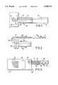
- FIG. 1is a plan view of an antenna system
- FIG. 2illustrates schematically the currents in the various parts of the antenna system
- FIG. 3illustrates an antenna system incorporated in a wireless terminal
- FIG. 4shows a prior art arrangement
- FIG. 5illustrates a polarization diversity unit
- FIG. 6illustrates the associated switching circuit
- FIG. 7illustrates an antenna array based on antenna systems according to the invention.
- FIG. 1illustrates an antenna system, indicated generally as 10, which comprises first and second conductive strips 12, 14 on a printed circuit board (PCB) 16.
- Strips 12, 14are on the lower side of the PCB as viewed in FIG. 1, and are therefore shown in dashed outline.
- Each stripis L/4 in length where L is the wavelength of operation, and strips are connected end-to-end.
- the end of strip 12 remote from strip 14is connected to one side of a radio frequency (RF) generator 18 operating at wavelength L.
- RFradio frequency
- strip 22is straight and of length L/4 and one end is connected to the other side of the generator 18.
- Strip 24is essentially "L" shaped, the longer arm of the L lying parallel to and spaced from strip part 22, and the shorter arm being connected to the opposite end of strip 22 to the generator connection.
- Adjacent strips 22, 24is a fifth conducting strip 26 perpendicular to the other four strips.
- Strip 26is of relatively small size and provides a suitable connection for unbalanced feed means such as a coaxial feed cable (not shown) which connects the RF source 18 to the antenna. It will be appreciated that with this arrangement, the provision of a true ground plane, which would need to be of much greater size than strip 26, is unnecessary.
- Strip 22overlies strip 12, i.e., strips are in register but are separated by the thickness of PCB 16.
- PCB 16advantageously follows the general elongated outline of the strips but is of slightly greater area.
- both sides of the PCB 16are shown in a schematic view.
- strips 12, 14, and below the chain dashed lineare strips 22, 24 and strip 26. While strips 12, 14 are shown to be thinner than strips 22, 24, this is for clarity of illustration only; the strips in practice may be of equal width.
- strip 14 attached to strip 12can be regarded as a L/4 monopole with respect to the virtual ground positioned at the end of strip 22 underneath the junction of strips 12 and 14.
- the RF generatorhas moved to the other end of the line formed by strips 12, 22 and has one of its outputs connected to strip 14 and the other floating.
- the RF currents I 24 and I 14are of equal amplitude and orientation, as in the case of a center fed dipole, while the unbalanced RF generator 18 appears to feed unbalanced monopole antenna 14, through microstrip line 12, 22.
- the RF currents I 12 and I 22cancel each other in terms of radiation, while currents I 14 and I 24 act together as a center fed dipole. More precisely the currents in strips 14 and 24 are distributed in the same way as in the arms of a center fed dipole, creating its effect of a true dipole-like radiation pattern.
- the dipole 14, 24is in fact end fed (through line 12, 22), and thus has the convenience of an end fed antenna.
- FIG. 3is a view of a hand held wireless terminal 30 comprising a metalized housing 32 carrying call buttons 34 and a display panel 36.
- the housing 32contains the RF generator 18, and from the housing projects a long narrow PCB 16 carrying strips 12, 14 on the reverse side (and therefore shown dashed) and strips 22, 24 on the upper side, strips being connected to opposite sides of the generator 18 as shown in the Fig.
- FIG. 4shows a prior art hand held wireless terminal 40 comprising a metal casing 42, buttons 44, and display panel 46, and also having a quarter wavelength monopole antenna, or whip antenna, 48.
- the current I 48 passing along itis the main source of electromagnetic radiation.
- the use of the inventive antenna systemresults in the RF currents being confined mainly to the antenna, and the casing 32 is almost free of surface currents.
- the RF loss by absorption by the user's handis minimized, giving a performance improvement of up to 3 dB.
- the convenience of the end-fed formatis clear from the figure.
- FIG. 5two antenna systems according to the invention are shown on a triangular PCB 54.
- the two sets of strips 56, 57, 61 and 62, on the upper surface of the PCB as viewed (and shown shaded)are arranged orthogonally; on the lower surface, and, therefore, indicated in dashed outline, are the respective folded strip arrangements 58 and 60, and a conductive connection area 64, here shown as a square.
- the respective antenna systemsare indicated as A5 and A6.
- the connections between the generator 18 and the systems A5, A6pass through the conductive connection area 64 and feed connection 63 in this arrangement.
- any two antenna systems according to the inventionif collocated and arranged orthogonally, retain 20 dB isolation between them.
- This low cross polarizationallows the arrangement of FIG. 5 to be used as a polarization diversity antenna unit, i.e. a unit in which one antenna system may be selected when it gives the stronger signal.
- a selection circuitis shown in FIG. 6, with the antenna systems A5 and A6 shown schematically.
- the feed ends of the antenna systemsare connected through a series arrangement of two diodes at 70, 72 and there is an RF generator and DC supply 68 connected between the diodes.
- the RF supply line to each antennais provided with a respective current sink resistor 74, 76.
- the RF and DC unit 68is connected to signal transceiver means 78.
- the DC current supplyis positive and passes to antenna A5 through diode 72; as the signal received from this antenna system fades, the current is switched to negative, so that the other antenna system A6 is brought into operation.
- the resistors 74, 76are each one Kilo Ohm, and the switching diodes 70, 72 are low cost PIN diodes with very low leads inductance.
- the diodes 70, 72are located in the gaps between strips 57, 62 and the feed connection 63, respectively, shown in FIG. 5.
- the 20 dB isolation between the antenna systemsis roughly equal to the depth of the Rayleigh fading in an indoor radio channel.
- the arrangement of FIGS. 5 and 6may be applied to permit switching from one antenna to the other to counteract this.
- the FIG. 5 arrangementmay be provided in an adapter for use in an indoor radio channel to allow the connection of personal computers.
- FIG. 7illustrates an antenna array.
- the arrayis provided on a double sided PCB 84 and has N antenna systems, A 1 , A 2 , A 3 . . . A N each comprising a linear half wavelength strip L 1 , L 2 , L 3 . . . L N on one side of the PCB and shown blocked in, and a folded half wavelength strip F 1 , F 2 , F 3 . . . F N on the other side of the PCB.
- the feed ends of the antennaeare interconnected by conventional microstrip lines 86.
- a phase shifter P 1 , P 2 , P.sub.(N-1)is connected between each adjacent pair of systems; the first system is connected directly to a RF generator 88, and subsequent systems are supplied through the phase shifters P in series.
- the arrangementis such that there is a phase delay ⁇ between each adjacent pair of antennae systems, the phase delay increasing along the array, and each antenna system has almost purely linear polarization. The array can therefore be steered. It will be clear that the higher the number N of systems, the higher the directivity and gain of the antenna array.
- the microstrip lines 86give very easy access to the individual antenna systems.
Landscapes
- Variable-Direction Aerials And Aerial Arrays (AREA)
Abstract
Description
Claims (6)
Applications Claiming Priority (2)
| Application Number | Priority Date | Filing Date | Title |
|---|---|---|---|
| GB9516564 | 1995-08-12 | ||
| GBGB9516564.3AGB9516564D0 (en) | 1995-08-12 | 1995-08-12 | Compact antenna |
Publications (1)
| Publication Number | Publication Date |
|---|---|
| US5598174Atrue US5598174A (en) | 1997-01-28 |
Family
ID=10779160
Family Applications (1)
| Application Number | Title | Priority Date | Filing Date |
|---|---|---|---|
| US08/538,316Expired - LifetimeUS5598174A (en) | 1995-08-12 | 1995-10-03 | Printed sleeve antenna |
Country Status (2)
| Country | Link |
|---|---|
| US (1) | US5598174A (en) |
| GB (1) | GB9516564D0 (en) |
Cited By (16)
| Publication number | Priority date | Publication date | Assignee | Title |
|---|---|---|---|---|
| US5754145A (en)* | 1995-08-23 | 1998-05-19 | U.S. Philips Corporation | Printed antenna |
| EP0969546A1 (en)* | 1998-06-30 | 2000-01-05 | Lucent Technologies Inc. | Phase delay line for collinear array antenna |
| US6346916B1 (en)* | 1999-02-26 | 2002-02-12 | Kabushiki Kaisha Toshiba | Antenna apparatus and radio device using antenna apparatus |
| US6377227B1 (en) | 1999-04-28 | 2002-04-23 | Superpass Company Inc. | High efficiency feed network for antennas |
| US20020175804A1 (en)* | 2001-05-22 | 2002-11-28 | Takeshi Saito | Interrogator and goods management system adopting the same |
| US6538614B2 (en) | 2001-04-17 | 2003-03-25 | Lucent Technologies Inc. | Broadband antenna structure |
| US20030075604A1 (en)* | 2000-09-19 | 2003-04-24 | International Business Machines Corporation | Connecting structure of card, card, and computer system |
| US6559809B1 (en)* | 2001-11-29 | 2003-05-06 | Qualcomm Incorporated | Planar antenna for wireless communications |
| US6580397B2 (en)* | 2000-10-27 | 2003-06-17 | Telefonaktiebolaget L M Ericsson (Publ) | Arrangement for a mobile terminal |
| US20040056805A1 (en)* | 2002-09-24 | 2004-03-25 | Gemtek Technology Co., Ltd. | Multi-frequency printed antenna |
| US20040217912A1 (en)* | 2003-04-25 | 2004-11-04 | Mohammadian Alireza Hormoz | Electromagnetically coupled end-fed elliptical dipole for ultra-wide band systems |
| US20050035911A1 (en)* | 2003-04-01 | 2005-02-17 | Pih-Si Cheng | Dual-band antenna |
| US20080079640A1 (en)* | 2006-10-02 | 2008-04-03 | Airgain, Inc. | Compact multi-element antenna with phase shift |
| US20080150823A1 (en)* | 2004-11-29 | 2008-06-26 | Alireza Hormoz Mohammadian | Compact antennas for ultra wide band applications |
| US20100134377A1 (en)* | 2008-11-28 | 2010-06-03 | Asustek Computer Inc. | Planar antenna |
| US20130214982A1 (en)* | 2012-02-16 | 2013-08-22 | Stuart James Dean | Dipole antenna element with independently tunable sleeve |
Citations (4)
| Publication number | Priority date | Publication date | Assignee | Title |
|---|---|---|---|---|
| US4015265A (en)* | 1974-07-18 | 1977-03-29 | Etat Francais | Folded doublet antenna |
| US5182570A (en)* | 1989-11-13 | 1993-01-26 | X-Cyte Inc. | End fed flat antenna |
| US5440317A (en)* | 1993-05-17 | 1995-08-08 | At&T Corp. | Antenna assembly for a portable transceiver |
| US5495260A (en)* | 1993-08-09 | 1996-02-27 | Motorola, Inc. | Printed circuit dipole antenna |
- 1995
- 1995-08-12GBGBGB9516564.3Apatent/GB9516564D0/enactivePending
- 1995-10-03USUS08/538,316patent/US5598174A/ennot_activeExpired - Lifetime
Patent Citations (4)
| Publication number | Priority date | Publication date | Assignee | Title |
|---|---|---|---|---|
| US4015265A (en)* | 1974-07-18 | 1977-03-29 | Etat Francais | Folded doublet antenna |
| US5182570A (en)* | 1989-11-13 | 1993-01-26 | X-Cyte Inc. | End fed flat antenna |
| US5440317A (en)* | 1993-05-17 | 1995-08-08 | At&T Corp. | Antenna assembly for a portable transceiver |
| US5495260A (en)* | 1993-08-09 | 1996-02-27 | Motorola, Inc. | Printed circuit dipole antenna |
Cited By (28)
| Publication number | Priority date | Publication date | Assignee | Title |
|---|---|---|---|---|
| US5754145A (en)* | 1995-08-23 | 1998-05-19 | U.S. Philips Corporation | Printed antenna |
| JP3420532B2 (en) | 1998-06-30 | 2003-06-23 | ルーセント テクノロジーズ インコーポレーテッド | Phase delay line for collinear array antenna |
| EP0969546A1 (en)* | 1998-06-30 | 2000-01-05 | Lucent Technologies Inc. | Phase delay line for collinear array antenna |
| US6222494B1 (en) | 1998-06-30 | 2001-04-24 | Agere Systems Guardian Corp. | Phase delay line for collinear array antenna |
| US6346916B1 (en)* | 1999-02-26 | 2002-02-12 | Kabushiki Kaisha Toshiba | Antenna apparatus and radio device using antenna apparatus |
| US6377227B1 (en) | 1999-04-28 | 2002-04-23 | Superpass Company Inc. | High efficiency feed network for antennas |
| US6942149B2 (en)* | 2000-09-19 | 2005-09-13 | International Business Machines Corporation | Connecting structure of card, card, and computer system |
| US20030075604A1 (en)* | 2000-09-19 | 2003-04-24 | International Business Machines Corporation | Connecting structure of card, card, and computer system |
| US6580397B2 (en)* | 2000-10-27 | 2003-06-17 | Telefonaktiebolaget L M Ericsson (Publ) | Arrangement for a mobile terminal |
| US6538614B2 (en) | 2001-04-17 | 2003-03-25 | Lucent Technologies Inc. | Broadband antenna structure |
| US7164380B2 (en)* | 2001-05-22 | 2007-01-16 | Hitachi, Ltd. | Interrogator and goods management system adopting the same |
| US20020175804A1 (en)* | 2001-05-22 | 2002-11-28 | Takeshi Saito | Interrogator and goods management system adopting the same |
| US6559809B1 (en)* | 2001-11-29 | 2003-05-06 | Qualcomm Incorporated | Planar antenna for wireless communications |
| US6906678B2 (en)* | 2002-09-24 | 2005-06-14 | Gemtek Technology Co. Ltd. | Multi-frequency printed antenna |
| US20040056805A1 (en)* | 2002-09-24 | 2004-03-25 | Gemtek Technology Co., Ltd. | Multi-frequency printed antenna |
| US6891504B2 (en) | 2003-04-01 | 2005-05-10 | Wistron Neweb Corporation | Dual-band antenna |
| US20050035911A1 (en)* | 2003-04-01 | 2005-02-17 | Pih-Si Cheng | Dual-band antenna |
| US20040217912A1 (en)* | 2003-04-25 | 2004-11-04 | Mohammadian Alireza Hormoz | Electromagnetically coupled end-fed elliptical dipole for ultra-wide band systems |
| US7973733B2 (en) | 2003-04-25 | 2011-07-05 | Qualcomm Incorporated | Electromagnetically coupled end-fed elliptical dipole for ultra-wide band systems |
| US20080150823A1 (en)* | 2004-11-29 | 2008-06-26 | Alireza Hormoz Mohammadian | Compact antennas for ultra wide band applications |
| US8059054B2 (en) | 2004-11-29 | 2011-11-15 | Qualcomm, Incorporated | Compact antennas for ultra wide band applications |
| US20080079640A1 (en)* | 2006-10-02 | 2008-04-03 | Airgain, Inc. | Compact multi-element antenna with phase shift |
| US8081123B2 (en)* | 2006-10-02 | 2011-12-20 | Airgain, Inc. | Compact multi-element antenna with phase shift |
| US20120086604A1 (en)* | 2006-10-02 | 2012-04-12 | Xiao Ping Yang | Compact Multi-Element Antenna With Phase Shift |
| US8310402B2 (en)* | 2006-10-02 | 2012-11-13 | Airgain, Inc. | Compact multi-element antenna with phase shift |
| US20100134377A1 (en)* | 2008-11-28 | 2010-06-03 | Asustek Computer Inc. | Planar antenna |
| US20130214982A1 (en)* | 2012-02-16 | 2013-08-22 | Stuart James Dean | Dipole antenna element with independently tunable sleeve |
| US8830135B2 (en)* | 2012-02-16 | 2014-09-09 | Ultra Electronics Tcs Inc. | Dipole antenna element with independently tunable sleeve |
Also Published As
| Publication number | Publication date |
|---|---|
| GB9516564D0 (en) | 1995-10-11 |
Similar Documents
| Publication | Publication Date | Title |
|---|---|---|
| US5598174A (en) | Printed sleeve antenna | |
| EP0969546B1 (en) | Phase delay line for collinear array antenna | |
| KR100526585B1 (en) | Planar antenna with circular and linear polarization. | |
| US5532708A (en) | Single compact dual mode antenna | |
| US5754145A (en) | Printed antenna | |
| US6307525B1 (en) | Multiband flat panel antenna providing automatic routing between a plurality of antenna elements and an input/output port | |
| US6339404B1 (en) | Diversity antenna system for lan communication system | |
| US6424311B1 (en) | Dual-fed coupled stripline PCB dipole antenna | |
| EP1025614B1 (en) | Compact antenna structures including baluns | |
| US6400332B1 (en) | PCB dipole antenna | |
| US5448250A (en) | Laminar microstrip patch antenna | |
| US6025811A (en) | Closely coupled directional antenna | |
| EP0762542A2 (en) | Diversity antenna circuit | |
| US7042412B2 (en) | Printed dual dipole antenna | |
| US7764242B2 (en) | Broadband antenna system | |
| CA2270302A1 (en) | High efficiency printed antennas | |
| EP1206000A2 (en) | Portable communication terminal with reduced specific absorption rate | |
| US11264730B2 (en) | Quad-port radiating element | |
| US6259416B1 (en) | Wideband slot-loop antennas for wireless communication systems | |
| US4740793A (en) | Antenna elements and arrays | |
| KR100449857B1 (en) | Wideband Printed Dipole Antenna | |
| JP3378513B2 (en) | Planar directional antenna | |
| JPH01147905A (en) | Plane antenna | |
| CN1156941C (en) | dipole antenna combination | |
| JP2006014157A (en) | Balun device and antenna device |
Legal Events
| Date | Code | Title | Description |
|---|---|---|---|
| AS | Assignment | Owner name:AT&T CORP., NEW YORK Free format text:ASSIGNMENT OF ASSIGNORS INTEREST;ASSIGNORS:ERKOCEVIC, NEDIM;JANSEN, AUGUSTINUS MARIA;REEL/FRAME:007860/0528 Effective date:19950920 | |
| AS | Assignment | Owner name:LUCENT TECHNOLOGIES INC., NEW JERSEY Free format text:ASSIGNMENT OF ASSIGNORS INTEREST;ASSIGNOR:AT&T CORP.;REEL/FRAME:008196/0181 Effective date:19960329 | |
| STCF | Information on status: patent grant | Free format text:PATENTED CASE | |
| FEPP | Fee payment procedure | Free format text:PAYOR NUMBER ASSIGNED (ORIGINAL EVENT CODE: ASPN); ENTITY STATUS OF PATENT OWNER: LARGE ENTITY | |
| FPAY | Fee payment | Year of fee payment:4 | |
| FPAY | Fee payment | Year of fee payment:8 | |
| FPAY | Fee payment | Year of fee payment:12 | |
| AS | Assignment | Owner name:DEUTSCHE BANK AG NEW YORK BRANCH, AS COLLATERAL AG Free format text:PATENT SECURITY AGREEMENT;ASSIGNORS:LSI CORPORATION;AGERE SYSTEMS LLC;REEL/FRAME:032856/0031 Effective date:20140506 | |
| AS | Assignment | Owner name:AGERE SYSTEMS GUARDIAN CORP., PENNSYLVANIA Free format text:ASSIGNMENT OF ASSIGNORS INTEREST;ASSIGNOR:LUCENT TECHNOLOGIES INC.;REEL/FRAME:035000/0144 Effective date:20010201 Owner name:AVAGO TECHNOLOGIES GENERAL IP (SINGAPORE) PTE. LTD Free format text:ASSIGNMENT OF ASSIGNORS INTEREST;ASSIGNOR:AGERE SYSTEMS LLC;REEL/FRAME:035059/0001 Effective date:20140804 Owner name:AGERE SYSTEMS LLC, PENNSYLVANIA Free format text:MERGER;ASSIGNOR:AGERE SYSTEMS INC.;REEL/FRAME:035058/0895 Effective date:20120724 Owner name:AGERE SYSTEMS INC., PENNSYLVANIA Free format text:MERGER;ASSIGNOR:AGERE SYSTEMS GUARDIAN CORP.;REEL/FRAME:035058/0884 Effective date:20020822 | |
| AS | Assignment | Owner name:LSI CORPORATION, CALIFORNIA Free format text:TERMINATION AND RELEASE OF SECURITY INTEREST IN PATENT RIGHTS (RELEASES RF 032856-0031);ASSIGNOR:DEUTSCHE BANK AG NEW YORK BRANCH, AS COLLATERAL AGENT;REEL/FRAME:037684/0039 Effective date:20160201 Owner name:AGERE SYSTEMS LLC, PENNSYLVANIA Free format text:TERMINATION AND RELEASE OF SECURITY INTEREST IN PATENT RIGHTS (RELEASES RF 032856-0031);ASSIGNOR:DEUTSCHE BANK AG NEW YORK BRANCH, AS COLLATERAL AGENT;REEL/FRAME:037684/0039 Effective date:20160201 |