US5598095A - Switchable current source for digital-to-analog converter (DAC) - Google Patents
Switchable current source for digital-to-analog converter (DAC)Download PDFInfo
- Publication number
- US5598095A US5598095AUS08/401,022US40102295AUS5598095AUS 5598095 AUS5598095 AUS 5598095AUS 40102295 AUS40102295 AUS 40102295AUS 5598095 AUS5598095 AUS 5598095A
- Authority
- US
- United States
- Prior art keywords
- current
- transistor
- source
- output
- enable signal
- Prior art date
- Legal status (The legal status is an assumption and is not a legal conclusion. Google has not performed a legal analysis and makes no representation as to the accuracy of the status listed.)
- Expired - Lifetime
Links
- 230000007704transitionEffects0.000claimsabstractdescription19
- 230000000295complement effectEffects0.000claims3
- 230000004044responseEffects0.000abstractdescription6
- 230000003111delayed effectEffects0.000abstract2
- 229920005994diacetyl cellulosePolymers0.000abstract1
- 230000006870functionEffects0.000description6
- 238000000034methodMethods0.000description5
- 238000006243chemical reactionMethods0.000description4
- 238000010586diagramMethods0.000description4
- 230000008901benefitEffects0.000description3
- 230000008859changeEffects0.000description3
- 230000000694effectsEffects0.000description3
- 238000004519manufacturing processMethods0.000description3
- 230000008569processEffects0.000description3
- 230000001934delayEffects0.000description2
- 230000009471actionEffects0.000description1
- 230000002411adverseEffects0.000description1
- 230000006872improvementEffects0.000description1
- 230000005923long-lasting effectEffects0.000description1
- 230000009467reductionEffects0.000description1
- 230000007480spreadingEffects0.000description1
Images

Classifications
- G—PHYSICS
- G05—CONTROLLING; REGULATING
- G05F—SYSTEMS FOR REGULATING ELECTRIC OR MAGNETIC VARIABLES
- G05F3/00—Non-retroactive systems for regulating electric variables by using an uncontrolled element, or an uncontrolled combination of elements, such element or such combination having self-regulating properties
- G05F3/02—Regulating voltage or current
- G05F3/08—Regulating voltage or current wherein the variable is DC
- G05F3/10—Regulating voltage or current wherein the variable is DC using uncontrolled devices with non-linear characteristics
- G05F3/16—Regulating voltage or current wherein the variable is DC using uncontrolled devices with non-linear characteristics being semiconductor devices
- G05F3/20—Regulating voltage or current wherein the variable is DC using uncontrolled devices with non-linear characteristics being semiconductor devices using diode- transistor combinations
- G05F3/26—Current mirrors
- G05F3/262—Current mirrors using field-effect transistors only
Definitions
- the present inventionrelates generally to switchable current sources, and more specifically to switchable current sources for current scaling video digital-to-analog converters (DACs).
- DACsdigital-to-analog converters
- the general family of DACsincludes both voltage scaling, charge scaling and current scaling designs.
- a number of binary weighted circuitsare selectively summed at a common node according to a digital input. Due to changes in node voltages, voltage scaling DACs produce switching transients that can result in conversion errors unless an appropriate settling time is taken into consideration.
- Current scaling DACscontain a number of switchable current sources that selectively switch an output current into a current summing node in response to a digital input signal.
- Each switchable current sourcecan be conceptualized as having a current source, and a current switch.
- the current sourcefunctions to provides a binary weighted output current.
- current mirrorsImproved current mirrors are set forth in U.S. Pat. No. 3,936,725 issued to Herbert A. Schneider on Feb. 3, 1976.
- the current switchpositioned between the current source and the summing node, switches the output current into the summing node according to the digital input.
- each switchable current sourcewhen switched on, provide a reliable, precise output current to the summing node. Accordingly, it would be desirable to have a switchable current source with a current magnitude determining circuit that is isolated from the current switch.
- the switching action of a given individual switchable current sourcecan also contribute to, or generate by itself, output transients.
- Output transientsare particularly bothersome to video DACs because they can result in distracting anomalies on the video display screen.
- the preferred embodiment of the present inventionis a switchable current source for providing a weighted output current to an output node in response to an enable signal.
- the present inventionincludes a current source and a current switch.
- the current sourceprovides an output current in response to a reference current, and is formed by a current mirror connected in a cascode arrangement to a cascode pair of transistors. Both the current mirror and the cascode pair are formed by two p-channel transistors.
- the current mirroris coupled to the supply voltage and the cascode pair is coupled to the current mirror.
- the cascode pairprovides an input reference current node and an output current node.
- a reference currentis provided to the input reference current node by a reference current source.
- a current switchis connected to the output current node and provides alternate switch paths; a first current path to ground and a second current path to the output node.
- the switchable current sourceswitches between and “on” state and an “off” state in response to an enable signal provided by an enable signal source.
- the current switchIn the off state, the current switch provides the first current path to ground. In the on state the first current path is disabled and the second current path to the output node is provided.
- the current switch and enable signalare designed so that in an off-to-on transition the second current path is provided prior to disabling the first current path. In a similar fashion, in an on-to-off transition the first current path is provided prior to disabling the second current path. This "make-before-break" operation of the current switch has been found to greatly reduce output transients in DACs employing the present invention.
- An advantage of the present inventionis that it can be realized with current source transistors having a smaller channel length than that of the prior art.
- FIG. 1is a block schematic diagram illustrating the preferred embodiment of the present invention.
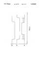
- FIG. 2is a block schematic diagram illustrating the enable signal generator of the preferred embodiment of the present invention.
- FIG. 3is a timing diagram illustrating the operation of the enable signal generator.
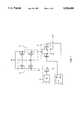
- the preferred embodiment of the present inventionis a switchable current source and is set forth in detail in FIG. 1, and designated by the general reference character 10.
- the switchable current sourcecan be conceptualized as being composed of a current source 12, a reference current generator 14, a current switch 16 and an enable signal generator 18.
- the current source 12 of the preferred embodiment 10includes a current mirror 20 and a cascode pair 22.
- the current mirror 20includes a first PMOS transistor Q1 and a second PMOS transistor Q2. Both Q1 and Q2 are connected by their respective sources to the positive supply voltage Vcc.
- Q1 and Q2are gate coupled, with Q1 having its gate further connected to its drain.
- the cascode pair 22is similar to the current mirror 20 being composed of two gate-coupled PMOS transistors Q3 and Q4, the gate of Q3 being further connected to its drain.
- the cascode pair 22is coupled to the current mirror 20 by connecting the drains of Q1 and Q2 to the sources of Q3 and Q4, respectively.
- the current source 12provides an output current in response to a reference current.
- the reference currentis supplied at node N1, and an output current is generated at node N2.
- the transistor pairs making up the current mirror and cascode pair (20 and 22) of the preferred embodiment 10are scaled. That is, the channel width-to-length ratio (W/L) of Q2 and Q4 are three times than that of Q1 and Q3. This allows for a more compact design, enabling the smaller transistors to control the larger ones. While the preferred embodiment employs a 1:3 ratio, it is understood that other ratios may be selected.
- the present inventorhas found that combination of current mirror 20 with cascode pair 22 provides a stable voltage level at node N3. As current is drawn through the current source 12, any source-drain voltage drop occurs between node N2 and node N3, with the source-drain voltage between N3 and Vcc remaining relatively constant. This reduces current variations and transients in the current source 12 and allows Q2 to be designed with a smaller channel length than prior art designs. This reduces the overall layout size of the circuit. In addition, because transistors Q1, Q3 and Q5 are isolated from any switching functions, switching does not adversely affect bias conditions of the current mirror 20 and consequently, the current supplied remains stable during all phases of operation.
- the reference current generator 14 of the preferred embodiment 10includes a voltage generator 24 and a PMOS transistor Q5. Referring once again to FIG. 1, it is shown that Q5 is connected by its source to node N1, by its gate to the voltage generator 24, and by its drain to ground. A reference current is supplied at N1 according to the biasing voltage applied to the gate of Q5 by the voltage generator 24.
- the type and arrangement of the voltage generator 24is not critical to the invention and so will not be set forth in detail herein. All that is necessary is for the appropriate voltage to be applied to generate the desired reference current. It is noted that in the preferred embodiment 10, the reference current generated is one third of the desired output current, due to the W/L ratios of the transistors in the current source 20 and the cascode pair 22. Accordingly, once the desired gate voltage is applied to Q5 an output current will be present at node N2.
- the current switch 16includes two PMOS transistors Q6 and Q7.
- Q6 and Q7are connected by their respective sources to node N2.
- the drain of Q6is connected to ground, and the drain of Q7 is connected to an output node N4.
- the gates of both Q6 and Q7are connected to the enable signal generator 18, with Q6 receiving an enable signal "EN", and Q7 receiving an inverted enable signal "ENI”.
- the enable signal generator 18is set forth in detail in FIG. 2. As illustrated in the figure the enable signal generator 18 receives a decoder input "DEC" and provides the EN and ENI output signals.
- the enable signal generatoris shown to include a first branch 26 and a second branch 28.
- the first branch 26receives the DEC signal and then splits down a first delay path 30 and a first direct path 32.
- the two paths (30 and 32)terminate as mutual inputs to a NAND gate G1.
- G1provides an output to inverter I1, which in turn, provides the EN signal.
- the second branch 28is similar to the first branch, having a second delay path 34, a second direct path 36, a NAND gate G2 and an inverter I2 arranged in a similar fashion.
- the second branch 28differs from the first in that the DEC signal first passes through an inverter I3, prior to entering the second delay path 34 and second direct path 36.
- the delay paths (30 and 34)are formed by four successive delay inverters, each identified as I4.
- the inverters I4function to delay the propagation of the DEC signal down their respective paths.
- ENis coupled to the gate of Q6 and ENI to the gate of Q7. From the timing of EN and ENI illustrated in FIG. 3, it is shown that EN and ENI drive transistors Q6 and Q7 in a "make-before-break" switching arrangement between ground and the output node N4.
- EN and ENIdrive transistors Q6 and Q7 in a "make-before-break" switching arrangement between ground and the output node N4.
- the inventorhas found the "make before break" switching arrangement greatly reduces any transients generated by switching the current source 12 to the output node. Absent such switch timing the current source 12 can be briefly interrupted, and voltage transients can develop at node N4, despite the advantages of the current mirror 20/cascode pair 22 design. As a result, time would be required to reestablish stable behavior in the current source 12. While the preferred embodiment sets forth a "make before break" switching arrangement with a particular current source 12, it is understood the same switching arrangement may be applied to other current sources to reduce output transients.
- the switchable current source of the present invention 10is primarily intended for use in video digital-to-analog converters (DACs). However, the present invention 10 may be utilized in any application wherein conventional DACs are used.
- the main area of improvementis the reduction in the magnitude of transients produced when the output current of the weighted current sources are switched to a common current summing node.
- switchable current source of the present inventionmay be readily constructed using present fabrication methods, it is expected that they will be acceptable in the industry as substitutes for conventional DAC current sources. For these and other reasons, it is expected that the utility and industrial applicability of the invention will be both significant in scope and long-lasting in duration.
Landscapes
- Engineering & Computer Science (AREA)
- Microelectronics & Electronic Packaging (AREA)
- Physics & Mathematics (AREA)
- Nonlinear Science (AREA)
- Electromagnetism (AREA)
- General Physics & Mathematics (AREA)
- Radar, Positioning & Navigation (AREA)
- Automation & Control Theory (AREA)
- Analogue/Digital Conversion (AREA)
Abstract
Description
Claims (20)
Priority Applications (1)
| Application Number | Priority Date | Filing Date | Title |
|---|---|---|---|
| US08/401,022US5598095A (en) | 1995-03-08 | 1995-03-08 | Switchable current source for digital-to-analog converter (DAC) |
Applications Claiming Priority (1)
| Application Number | Priority Date | Filing Date | Title |
|---|---|---|---|
| US08/401,022US5598095A (en) | 1995-03-08 | 1995-03-08 | Switchable current source for digital-to-analog converter (DAC) |
Publications (1)
| Publication Number | Publication Date |
|---|---|
| US5598095Atrue US5598095A (en) | 1997-01-28 |
Family
ID=23585948
Family Applications (1)
| Application Number | Title | Priority Date | Filing Date |
|---|---|---|---|
| US08/401,022Expired - LifetimeUS5598095A (en) | 1995-03-08 | 1995-03-08 | Switchable current source for digital-to-analog converter (DAC) |
Country Status (1)
| Country | Link |
|---|---|
| US (1) | US5598095A (en) |
Cited By (14)
| Publication number | Priority date | Publication date | Assignee | Title |
|---|---|---|---|---|
| US5883501A (en)* | 1996-04-19 | 1999-03-16 | Sony Corporation | Power supply circuit |
| US5892388A (en)* | 1996-04-15 | 1999-04-06 | National Semiconductor Corporation | Low power bias circuit using FET as a resistor |
| US5945821A (en)* | 1997-04-04 | 1999-08-31 | Citizen Watch Co., Ltd. | Reference voltage generating circuit |
| US6225929B1 (en) | 1998-12-02 | 2001-05-01 | Hewlett-Packard Company | Digital-to-analog converter having switchable current sources and resistor string |
| US6294939B1 (en)* | 1998-10-30 | 2001-09-25 | Stmicroelectronics, Inc. | Device and method for data input buffering |
| US6509855B1 (en)* | 2000-06-28 | 2003-01-21 | Intel Corporation | Digital-to-analog cell having reduced power consumption and method therefor |
| US6603338B1 (en) | 1998-10-30 | 2003-08-05 | Stmicroelectronics, Inc. | Device and method for address input buffering |
| WO2001093429A3 (en)* | 2000-05-25 | 2003-10-30 | Rockwell Tech Llc | Track/attenuate circuit and method for switched current source dac |
| US6667609B2 (en)* | 2000-03-28 | 2003-12-23 | Infineon Technologies Ag | Current generating device with reduced switching time from an energy saving mode |
| US6741195B1 (en) | 2002-12-11 | 2004-05-25 | Micron Technology, Inc. | Low glitch current steering digital to analog converter and method |
| US20090167424A1 (en)* | 2007-12-27 | 2009-07-02 | Sang-June Kim | Current cell circuit in digital-analog converter |
| US8537040B2 (en)* | 2011-11-15 | 2013-09-17 | Integrated Device Technology, Inc. | Data converter current sources using thin-oxide core devices |
| EP2207257A4 (en)* | 2007-10-02 | 2014-01-01 | Mitsubishi Electric Corp | GRID CONTROL CIRCUIT |
| TWI768973B (en)* | 2021-06-17 | 2022-06-21 | 瑞昱半導體股份有限公司 | Method for calibrating currents, current control system and voltage control system |
Citations (11)
| Publication number | Priority date | Publication date | Assignee | Title |
|---|---|---|---|---|
| US3936725A (en)* | 1974-08-15 | 1976-02-03 | Bell Telephone Laboratories, Incorporated | Current mirrors |
| US4016435A (en)* | 1974-03-11 | 1977-04-05 | U.S. Philips Corporation | Current stabilizing arrangement |
| US4229729A (en)* | 1978-05-19 | 1980-10-21 | Hughes Aircraft Company | Analog to digital converter utilizing a quantizer network |
| US4408190A (en)* | 1980-06-03 | 1983-10-04 | Tokyo Shibaura Denki Kabushiki Kaisha | Resistorless digital-to-analog converter using cascaded current mirror circuits |
| US4573005A (en)* | 1983-02-08 | 1986-02-25 | U.S. Philips Corporation | Current source arrangement having a precision current-mirror circuit |
| US4904922A (en)* | 1985-03-21 | 1990-02-27 | Brooktree Corporation | Apparatus for converting between digital and analog values |
| US4967140A (en)* | 1988-09-12 | 1990-10-30 | U.S. Philips Corporation | Current-source arrangement |
| US5166540A (en)* | 1990-03-10 | 1992-11-24 | Goldstar Electron Co., Ltd. | Stepped signal generating circuit |
| US5272432A (en)* | 1991-05-01 | 1993-12-21 | Winbond Electronics N.A. Corporation | DAC current source with stabilizing bias |
| US5285148A (en)* | 1991-08-23 | 1994-02-08 | Deutsche Itt Industries Gmbh | Current-regulating circuit having parallel control paths |
| US5430400A (en)* | 1993-08-03 | 1995-07-04 | Schlumberger Technologies Inc. | Driver circuits for IC tester |
- 1995
- 1995-03-08USUS08/401,022patent/US5598095A/ennot_activeExpired - Lifetime
Patent Citations (12)
| Publication number | Priority date | Publication date | Assignee | Title |
|---|---|---|---|---|
| US4016435A (en)* | 1974-03-11 | 1977-04-05 | U.S. Philips Corporation | Current stabilizing arrangement |
| US3936725A (en)* | 1974-08-15 | 1976-02-03 | Bell Telephone Laboratories, Incorporated | Current mirrors |
| US4229729A (en)* | 1978-05-19 | 1980-10-21 | Hughes Aircraft Company | Analog to digital converter utilizing a quantizer network |
| US4408190A (en)* | 1980-06-03 | 1983-10-04 | Tokyo Shibaura Denki Kabushiki Kaisha | Resistorless digital-to-analog converter using cascaded current mirror circuits |
| US4573005A (en)* | 1983-02-08 | 1986-02-25 | U.S. Philips Corporation | Current source arrangement having a precision current-mirror circuit |
| US4904922A (en)* | 1985-03-21 | 1990-02-27 | Brooktree Corporation | Apparatus for converting between digital and analog values |
| US4904922B1 (en)* | 1985-03-21 | 1992-09-01 | Apparatus for converting between digital and analog values | |
| US4967140A (en)* | 1988-09-12 | 1990-10-30 | U.S. Philips Corporation | Current-source arrangement |
| US5166540A (en)* | 1990-03-10 | 1992-11-24 | Goldstar Electron Co., Ltd. | Stepped signal generating circuit |
| US5272432A (en)* | 1991-05-01 | 1993-12-21 | Winbond Electronics N.A. Corporation | DAC current source with stabilizing bias |
| US5285148A (en)* | 1991-08-23 | 1994-02-08 | Deutsche Itt Industries Gmbh | Current-regulating circuit having parallel control paths |
| US5430400A (en)* | 1993-08-03 | 1995-07-04 | Schlumberger Technologies Inc. | Driver circuits for IC tester |
Cited By (15)
| Publication number | Priority date | Publication date | Assignee | Title |
|---|---|---|---|---|
| US5892388A (en)* | 1996-04-15 | 1999-04-06 | National Semiconductor Corporation | Low power bias circuit using FET as a resistor |
| US5883501A (en)* | 1996-04-19 | 1999-03-16 | Sony Corporation | Power supply circuit |
| US5945821A (en)* | 1997-04-04 | 1999-08-31 | Citizen Watch Co., Ltd. | Reference voltage generating circuit |
| US6603338B1 (en) | 1998-10-30 | 2003-08-05 | Stmicroelectronics, Inc. | Device and method for address input buffering |
| US6294939B1 (en)* | 1998-10-30 | 2001-09-25 | Stmicroelectronics, Inc. | Device and method for data input buffering |
| US6225929B1 (en) | 1998-12-02 | 2001-05-01 | Hewlett-Packard Company | Digital-to-analog converter having switchable current sources and resistor string |
| US6667609B2 (en)* | 2000-03-28 | 2003-12-23 | Infineon Technologies Ag | Current generating device with reduced switching time from an energy saving mode |
| WO2001093429A3 (en)* | 2000-05-25 | 2003-10-30 | Rockwell Tech Llc | Track/attenuate circuit and method for switched current source dac |
| US6509855B1 (en)* | 2000-06-28 | 2003-01-21 | Intel Corporation | Digital-to-analog cell having reduced power consumption and method therefor |
| US6741195B1 (en) | 2002-12-11 | 2004-05-25 | Micron Technology, Inc. | Low glitch current steering digital to analog converter and method |
| EP2207257A4 (en)* | 2007-10-02 | 2014-01-01 | Mitsubishi Electric Corp | GRID CONTROL CIRCUIT |
| US20090167424A1 (en)* | 2007-12-27 | 2009-07-02 | Sang-June Kim | Current cell circuit in digital-analog converter |
| US7782236B2 (en)* | 2007-12-27 | 2010-08-24 | Dongbu Hitek Co., Ltd | Current cell circuit in digital-analog converter |
| US8537040B2 (en)* | 2011-11-15 | 2013-09-17 | Integrated Device Technology, Inc. | Data converter current sources using thin-oxide core devices |
| TWI768973B (en)* | 2021-06-17 | 2022-06-21 | 瑞昱半導體股份有限公司 | Method for calibrating currents, current control system and voltage control system |
Similar Documents
| Publication | Publication Date | Title |
|---|---|---|
| US5598095A (en) | Switchable current source for digital-to-analog converter (DAC) | |
| KR100242905B1 (en) | Semiconductor circuit | |
| US5144173A (en) | Programmable delay line integrated circuit having programmable resistor circuit | |
| US7157941B2 (en) | Differential switching circuit and digital-to-analog converter | |
| KR20040098566A (en) | Level shift circuit | |
| KR900008802B1 (en) | Bimos logic circuitry | |
| US6288591B1 (en) | Level shifter for multiple supply voltage circuitry | |
| KR950002078B1 (en) | Level conversion circuit | |
| US4721866A (en) | CMOS current switching circuit | |
| KR930009432B1 (en) | Current element for digital / analog converter | |
| KR19990044240A (en) | Output buffer with shared intermediate node | |
| US20060097769A1 (en) | Level shift circuit and semiconductor circuit device including the level shift circuit | |
| KR930004351B1 (en) | Level shift circuit | |
| KR960010390B1 (en) | Switching constant current source circuit | |
| KR100429895B1 (en) | Level shifter having a plurlity of outputs | |
| US6211721B1 (en) | Multiplexer with short propagation delay and low power consumption | |
| JPS63300623A (en) | Semiconductor buffer circuit | |
| KR950008957B1 (en) | Digital/analog converter | |
| US6344761B2 (en) | Current comparison type latch | |
| JPH0556048B2 (en) | ||
| US5057713A (en) | Bipolar MOS logic circuit and semiconductor integrated circuit | |
| KR19980034655A (en) | Current Source Cell Device for Digital / Analog Converters | |
| US5160863A (en) | Delay circuit using primarily a transistor's parasitic capacitance | |
| JP3209967B2 (en) | Current cell and digital / analog converter using the same | |
| US5945851A (en) | Current source apparatus with bias switches |
Legal Events
| Date | Code | Title | Description |
|---|---|---|---|
| AS | Assignment | Owner name:ALLIANCE SEMICONDUCTOR CORPORATION, CALIFORNIA Free format text:ASSIGNMENT OF ASSIGNORS INTEREST;ASSIGNOR:SCHNAITTER, WILLIAM N.;REEL/FRAME:007389/0540 Effective date:19950307 | |
| STCF | Information on status: patent grant | Free format text:PATENTED CASE | |
| FPAY | Fee payment | Year of fee payment:4 | |
| FPAY | Fee payment | Year of fee payment:8 | |
| AS | Assignment | Owner name:ACACIA PATENT ACQUISITION CORPORATION, CALIFORNIA Free format text:OPTION;ASSIGNOR:ALLIANCE SEMICONDUCTOR CORPORATION;REEL/FRAME:019246/0001 Effective date:20070430 | |
| AS | Assignment | Owner name:ACACIA PATENT ACQUISTION CORPORATION, CALIFORNIA Free format text:ASSIGNMENT OF ASSIGNORS INTEREST;ASSIGNOR:ALLIANCE SEMICONDUCTOR CORPORATION;REEL/FRAME:019628/0979 Effective date:20070628 | |
| FPAY | Fee payment | Year of fee payment:12 | |
| AS | Assignment | Owner name:SHARED MEMORY GRAPHICS LLC, CALIFORNIA Free format text:ASSIGNMENT OF ASSIGNORS INTEREST;ASSIGNOR:ACACIA PATENT ACQUISITION LLC;REEL/FRAME:022892/0469 Effective date:20090601 |