US5597737A - Method for testing and burning-in a semiconductor wafer - Google Patents
Method for testing and burning-in a semiconductor waferDownload PDFInfo
- Publication number
- US5597737A US5597737AUS08/552,448US55244895AUS5597737AUS 5597737 AUS5597737 AUS 5597737AUS 55244895 AUS55244895 AUS 55244895AUS 5597737 AUS5597737 AUS 5597737A
- Authority
- US
- United States
- Prior art keywords
- bump
- bonding pads
- contacting
- semiconductor wafer
- under
- Prior art date
- Legal status (The legal status is an assumption and is not a legal conclusion. Google has not performed a legal analysis and makes no representation as to the accuracy of the status listed.)
- Expired - Lifetime
Links
Images


Classifications
- G—PHYSICS
- G01—MEASURING; TESTING
- G01R—MEASURING ELECTRIC VARIABLES; MEASURING MAGNETIC VARIABLES
- G01R31/00—Arrangements for testing electric properties; Arrangements for locating electric faults; Arrangements for electrical testing characterised by what is being tested not provided for elsewhere
- G01R31/28—Testing of electronic circuits, e.g. by signal tracer
- G01R31/282—Testing of electronic circuits specially adapted for particular applications not provided for elsewhere
- G01R31/2831—Testing of materials or semi-finished products, e.g. semiconductor wafers or substrates
- G—PHYSICS
- G01—MEASURING; TESTING
- G01R—MEASURING ELECTRIC VARIABLES; MEASURING MAGNETIC VARIABLES
- G01R31/00—Arrangements for testing electric properties; Arrangements for locating electric faults; Arrangements for electrical testing characterised by what is being tested not provided for elsewhere
- G01R31/28—Testing of electronic circuits, e.g. by signal tracer
- G01R31/2851—Testing of integrated circuits [IC]
- G01R31/2886—Features relating to contacting the IC under test, e.g. probe heads; chucks
Definitions
- the present inventionrelates to a method for testing and burning-in a semiconductor wafer generally, and more specifically to a method for testing a pre-bump semiconductor wafer to provide known good die.
- Flip-chip bondingis one method currently used in the semiconductor industry to physically and electrically connect a semiconductor die to the next level of interconnection wiring. Solder bumps are deposited on the bonding pads of a semiconductor die, and these solder bumps are then soldered to traces on the next level interconnect to link the die's internal functional portions to the next level interconnect. Typically, solder bumping and wafer probe test is done at the wafer level before the die are sent to assembly and test.
- a wafer reflow stepcan be performed after probing in an effort to regain the round bump shape, but if the deformation is extensive, the additional reflow step cannot cure this defect.
- the reflow stepis a cost adder.
- Another problem with the present method of probing bumped semiconductor wafersis that bump height variations across the wafer can cause some false readings of failures so that good die may erroneously be discarded due to false test results.
- lead oxide (Pb x O y ) from the solder bumpstends to stick to the probe tips thus requiring cleaning of the probe tips to eliminate the risk of contamination.
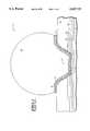
- FIG. 1illustrates, in cross-section, an enlarged view of a flip chip solder bump on a semiconductor die as known in the art.
- FIG. 2illustrates, in cross-section, an enlarged view of an under-bump-metallurgy on a bond pad of a semiconductor die.
- FIGS. 3-5illustrate, in cross-section, various methods for testing the semiconductor die through contacting the under-bump-metallurgy in accordance with the invention.
- the present inventionprovides a method for testing and burning-in a semiconductor wafer of flip-chip dice without deforming the solder bumps which are used to provide external electrical interconnects on flip-chip dice. Testing is done on the hard planar surface of the under-bump-metallurgy prior to the solder bumps being deposited.
- a probe tipconfigured either in an array or cantilevered arrangement, makes contact with the top layer of the under-bump-metallurgy, typically gold, on each bonding pad of each flip-chip die on the wafer. In this manner, known good die on the wafer level can be determined prior to the solder bumping process.
- FIG. 2Illustrated in FIG. 2 is a cross-sectional view of a bonding pad 14 of a semiconductor die 32.
- the bonding pad 14provides both the physical bond to the die surface and the electrical link into the actual circuitry of the semiconductor die. Additionally, the bonding pad provides an adhesive connection to the subsequently deposited solder bumps (as shown in FIG. 1).
- the bonding padis usually prepared by selectively depositing a series of localized under-bump-metallurgies onto a semiconductor wafer. Alternatively, a blanket film of these materials can be deposited directly onto the wafer and then selectively etched to leave the wettable bonding pads in the selected areas, namely overlying the bonding pads.
- the metallurgyis typically composed of a chrome-copper-gold stack, although titanium or titanium/tungsten can be used as alternatives to chrome, and nickel can be used as an alternative to copper.
- the gold layer at the top of the stackprevents oxidation of the copper in the under bump metallurgy.
- the total thickness of the layersis typically approximately 5,000 to 20,000 Angstroms ( ⁇ ).
- the bonding pad 14 of the semiconductor die 32is covered with a chrome-copper-gold under-bump-metallurgy (layers 16', 38 and 40, respectively) overlying metal line 22.
- a chrome-copper-gold under-bump-metallurgylayers 16', 38 and 40, respectively
- the under-bump-metallurgycan be deposited using conventional equipment and deposition techniques which are well known in the art. After the under-bump-metallurgy layers are formed but before the solder bumps are deposited, the semiconductor wafer can be tested or probed for opens and shorts, and then optionally burned-in, in accordance with the invention.
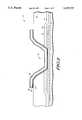
- FIGS. 3-5illustrate, in cross-section, various methods for testing the semiconductor die 32 through contacting the under-bump-metallurgy in accordance with the invention.
- a blunt array probe tip 42is shown positioned above the bonding pad. What is not illustrated is the remainder of the testing equipment to which the array probe tip 42 is attached.
- the testing equipmentcan be any of the commercially available tester for purposes of practicing the present invention.
- the blunt array probe tipwould move downward to contact the shoulder portions of the bonding pad to test for open/short of the device. Since the top layer of the under-bump-metallurgy is gold which is non-contaminating, there is no risk of lead contamination of the probe tip, which is an advantage over the prior art method of probing the solder bumps.
- FIG. 4illustrates a tapered array probe tip 44 which contacts the bonding pad 14. Because the probe tip 44 is tapered, it can contact the bonding pad in a central portion of the bonding pad. However, it is also possible for the tapered probe tip to contact the shoulder of the bonding pad 14 in a similar fashion to FIG. 3. For reliability reasons, it may be preferable to make contact on the shoulder portions of the bonding pad instead of within the trough of the pad.
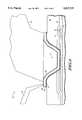
- FIG. 5illustrates two other types of probe tips that may be used in practicing the present invention.
- a tapered and pointed tip 46 of a cantilevered probe needleis illustrated making contact with the top layer 40 of the under-bump-metallurgy on the bonding pad 14.
- This pointed tip 46can have a typical tip radius of approximately 1.0 mil (25.4 ⁇ m) so as to be sufficiently rounded to prevent damage to the gold layer 40.
- a blunt tip 48 of a cantilevered probe needleis illustrated making contact with the top layer 40 of the under-bump-metallurgy.
- This blunt tip 48typically 5 mils (127 ⁇ m) in width, has the advantage of having a larger contact area so that the placement of the needle tip does not need to be as tightly and precisely controlled as the pointed tip 46.
- the pointed tip 46would be advantageous over the blunt tip 48 for contacting the bonding pad in the central portion or trough of the bonding pad as opposed to contacting it on the shoulder as shown.
- the semiconductor wafercan undergo an oxygen ash if required to reduce surface leakage.
- This oxygen ashcan be performed either after the semiconductor wafer has been tested at the wafer level by probing the under-bump-metallurgy and the good semiconductor dice on the wafer have been mapped, or the oxygen ash can be done after the under-bump-metallurgy has been formed but prior to wafer probe.
- an oxygen ashis intended to reduce current leakage between bonding pads by removing any organic contamination, such as carbonized polyimide, that occurs in the topmost layers of the polyimide layer 30. This oxygen ash is performed in the prior art on bumped wafers to reduce this surface leakage between solder bumps.
- a problem with the prior art methodis that the oxygen ash forms a thick oxide on the solder bumps which then adheres to the probe tips during test and burn-in causing contamination of the probes. Additionally, the presence of this oxide requires the use of an aggressive flux at assembly to achieve good wetting of the bumps to the next level interconnect.
- An advantage to performing the oxygen ash on semiconductor wafers prior to solder bumping, in accordance with the present invention,is that there are no solder bumps to oxidize. Hence, an aggressive flux cleaning step is not required at assembly thus eliminating a problem source causing marginal joining.
- solder bumpscan be deposited on the bonding pads of all the devices that passed testing and, optionally, burning-in to provide bumped known-good-die as desired in the semiconductor industry. Methods of forming traditional solder bumps are known in the art. In addition, methods for forming solder bumps having intrinsic potential for forming an extended eutectic region is disclosed in an allowed patent application, Ser. No. 08/236,320, now U.S. Pat. No. 5,470,787 by Stuart E. Greer, filed May 2, 1994, the teachings of which are herein incorporated by reference.
- the top layer of the under-bump-metallurgyis not limited to gold but may be another metal or any anti-oxidant barrier as long as it allows good joining between the under-bump-metallurgy and the solder bump. Therefore, it is intended that this invention encompass all such variations and modifications falling within the scope of the appended claims.
Landscapes
- Engineering & Computer Science (AREA)
- General Engineering & Computer Science (AREA)
- Physics & Mathematics (AREA)
- General Physics & Mathematics (AREA)
- Testing Or Measuring Of Semiconductors Or The Like (AREA)
- Measuring Leads Or Probes (AREA)
Abstract
Description
Claims (19)
Priority Applications (1)
| Application Number | Priority Date | Filing Date | Title |
|---|---|---|---|
| US08/552,448US5597737A (en) | 1995-11-03 | 1995-11-03 | Method for testing and burning-in a semiconductor wafer |
Applications Claiming Priority (1)
| Application Number | Priority Date | Filing Date | Title |
|---|---|---|---|
| US08/552,448US5597737A (en) | 1995-11-03 | 1995-11-03 | Method for testing and burning-in a semiconductor wafer |
Publications (1)
| Publication Number | Publication Date |
|---|---|
| US5597737Atrue US5597737A (en) | 1997-01-28 |
Family
ID=24205386
Family Applications (1)
| Application Number | Title | Priority Date | Filing Date |
|---|---|---|---|
| US08/552,448Expired - LifetimeUS5597737A (en) | 1995-11-03 | 1995-11-03 | Method for testing and burning-in a semiconductor wafer |
Country Status (1)
| Country | Link |
|---|---|
| US (1) | US5597737A (en) |
Cited By (26)
| Publication number | Priority date | Publication date | Assignee | Title |
|---|---|---|---|---|
| US5681758A (en)* | 1995-03-16 | 1997-10-28 | Komatsu Electronic Metals Co., Ltd. | Method for fabricating semiconductor single crystal |
| US5693565A (en)* | 1996-07-15 | 1997-12-02 | Dow Corning Corporation | Semiconductor chips suitable for known good die testing |
| US5766979A (en)* | 1996-11-08 | 1998-06-16 | W. L. Gore & Associates, Inc. | Wafer level contact sheet and method of assembly |
| US5958222A (en)* | 1997-11-17 | 1999-09-28 | Uop Llc | Standpipe distributor for short time contact of hydrocarbon compounds with particles |
| US5981370A (en)* | 1997-12-01 | 1999-11-09 | Texas Instruments Incorporated | Method for maximizing interconnection integrity and reliability between integrated circuits and external connections |
| US6337576B1 (en) | 1999-07-19 | 2002-01-08 | Alpine Microsystems, Inc. | Wafer-level burn-in |
| US6340895B1 (en) | 1999-07-14 | 2002-01-22 | Aehr Test Systems, Inc. | Wafer-level burn-in and test cartridge |
| US6413113B2 (en) | 1999-07-14 | 2002-07-02 | Aehr Test Systems | Kinematic coupling |
| US20020102832A1 (en)* | 1999-04-26 | 2002-08-01 | Katsumi Miyata | Semiconductor device and method of manufacturing the same |
| US6538326B2 (en)* | 2000-10-16 | 2003-03-25 | Sharp Kabushiki Kaisha | Semiconductor device and manufacturing method thereof |
| US6562636B1 (en) | 1999-07-14 | 2003-05-13 | Aehr Test Systems | Wafer level burn-in and electrical test system and method |
| US20030094963A1 (en)* | 2001-11-16 | 2003-05-22 | Jen-Kuang Fang | Device for testing electrical characteristics of chips |
| US6580283B1 (en) | 1999-07-14 | 2003-06-17 | Aehr Test Systems | Wafer level burn-in and test methods |
| US6599822B1 (en) | 1998-09-30 | 2003-07-29 | Micron Technology, Inc. | Methods of fabricating semiconductor substrate-based BGA interconnection |
| US20040005771A1 (en)* | 2001-09-10 | 2004-01-08 | Taiwan Semiconductor Manufacturing Company | Bumping process to increase bump height and to create a more robust bump structure |
| US20040018660A1 (en)* | 2002-07-27 | 2004-01-29 | Kim Su Hyeon | Method of fabricating multilayered UBM for flip chip interconnections by electroplating |
| US6933998B1 (en)* | 1999-12-01 | 2005-08-23 | Kawasaki Microelectronic, Inc. | Display devices with integrated control elements and methods of making devices |
| US20060131745A1 (en)* | 2004-12-14 | 2006-06-22 | Mitsubishi Denki Kabushiki Kaisha | Semiconductor device and manufacturing method therefor |
| US7102371B1 (en)* | 2004-05-19 | 2006-09-05 | National Semiconductor Corporation | Bilevel probe |
| US7319341B1 (en)* | 2003-08-28 | 2008-01-15 | Altera Corporation | Method of maintaining signal integrity across a capacitive coupled solder bump |
| US20090051379A1 (en)* | 2005-04-22 | 2009-02-26 | Alexander Leon | Method of treating and probing a via |
| US20090289253A1 (en)* | 2008-05-21 | 2009-11-26 | Stats Chippac, Ltd. | Semiconductor Wafer and Method of Forming Sacrificial Bump Pad for Wafer Probing During Wafer Sort Test |
| US20120178189A1 (en)* | 2011-01-06 | 2012-07-12 | Reber Douglas M | Method for forming an over pad metalization (opm) on a bond pad |
| US20150077148A1 (en)* | 2013-09-18 | 2015-03-19 | Seagate Technology Llc | Work piece contact pad with centering feature |
| US20180331000A1 (en)* | 2017-05-11 | 2018-11-15 | Invensas Bonding Technologies, Inc. | Probe methodology for ultrafine pitch Interconnects |
| DE102016100258B4 (en) | 2015-01-28 | 2024-06-27 | Infineon Technologies Ag | Method for forming an intermediate layer for copper structuring |
Citations (4)
| Publication number | Priority date | Publication date | Assignee | Title |
|---|---|---|---|---|
| US4950623A (en)* | 1988-08-02 | 1990-08-21 | Microelectronics Center Of North Carolina | Method of building solder bumps |
| US5289631A (en)* | 1992-03-04 | 1994-03-01 | Mcnc | Method for testing, burn-in, and/or programming of integrated circuit chips |
| US5470787A (en)* | 1994-05-02 | 1995-11-28 | Motorola, Inc. | Semiconductor device solder bump having intrinsic potential for forming an extended eutectic region and method for making and using the same |
| US5495667A (en)* | 1994-11-07 | 1996-03-05 | Micron Technology, Inc. | Method for forming contact pins for semiconductor dice and interconnects |
- 1995
- 1995-11-03USUS08/552,448patent/US5597737A/ennot_activeExpired - Lifetime
Patent Citations (4)
| Publication number | Priority date | Publication date | Assignee | Title |
|---|---|---|---|---|
| US4950623A (en)* | 1988-08-02 | 1990-08-21 | Microelectronics Center Of North Carolina | Method of building solder bumps |
| US5289631A (en)* | 1992-03-04 | 1994-03-01 | Mcnc | Method for testing, burn-in, and/or programming of integrated circuit chips |
| US5470787A (en)* | 1994-05-02 | 1995-11-28 | Motorola, Inc. | Semiconductor device solder bump having intrinsic potential for forming an extended eutectic region and method for making and using the same |
| US5495667A (en)* | 1994-11-07 | 1996-03-05 | Micron Technology, Inc. | Method for forming contact pins for semiconductor dice and interconnects |
Cited By (55)
| Publication number | Priority date | Publication date | Assignee | Title |
|---|---|---|---|---|
| US5681758A (en)* | 1995-03-16 | 1997-10-28 | Komatsu Electronic Metals Co., Ltd. | Method for fabricating semiconductor single crystal |
| US5693565A (en)* | 1996-07-15 | 1997-12-02 | Dow Corning Corporation | Semiconductor chips suitable for known good die testing |
| US5766979A (en)* | 1996-11-08 | 1998-06-16 | W. L. Gore & Associates, Inc. | Wafer level contact sheet and method of assembly |
| US6313411B1 (en) | 1996-11-08 | 2001-11-06 | W. L. Gore & Associates, Inc. | Wafer level contact sheet and method of assembly |
| US5958222A (en)* | 1997-11-17 | 1999-09-28 | Uop Llc | Standpipe distributor for short time contact of hydrocarbon compounds with particles |
| US5981370A (en)* | 1997-12-01 | 1999-11-09 | Texas Instruments Incorporated | Method for maximizing interconnection integrity and reliability between integrated circuits and external connections |
| US7126224B2 (en) | 1998-09-30 | 2006-10-24 | Micron Technology, Inc. | Semiconductor substrate-based interconnection assembly for semiconductor device bearing external connection elements |
| US6646286B1 (en)* | 1998-09-30 | 2003-11-11 | Micron Technology, Inc. | Semiconductor substrate-based BGA interconnection |
| US7061109B2 (en) | 1998-09-30 | 2006-06-13 | Micron Technology, Inc. | Semiconductor substrate-based BGA interconnection for testing semiconductor devices |
| US20040212092A1 (en)* | 1998-09-30 | 2004-10-28 | Salman Akram | Methods of fabricating semiconductor substrate-based BGA interconnections |
| US6740578B2 (en) | 1998-09-30 | 2004-05-25 | Micron Technology, Inc. | Methods of fabricating semiconductor substrate-based BGA interconnections |
| US20040004228A1 (en)* | 1998-09-30 | 2004-01-08 | Salman Akram | Methods of fabricating semiconductor substrate-based BGA interconnection |
| US6599822B1 (en) | 1998-09-30 | 2003-07-29 | Micron Technology, Inc. | Methods of fabricating semiconductor substrate-based BGA interconnection |
| US7276386B2 (en)* | 1999-04-26 | 2007-10-02 | Fujitsu Limited | Semiconductor device and method of manufacturing the same |
| US20020102832A1 (en)* | 1999-04-26 | 2002-08-01 | Katsumi Miyata | Semiconductor device and method of manufacturing the same |
| US20050006792A1 (en)* | 1999-04-26 | 2005-01-13 | Fujitsu Limited | Semiconductor device and method of manufacturing the same |
| US7619428B2 (en) | 1999-07-14 | 2009-11-17 | Aehr Test Systems | Wafer level burn-in and electrical test system and method |
| US7928754B2 (en) | 1999-07-14 | 2011-04-19 | Aehr Test Systems | Wafer level burn-in and electrical test system and method |
| US6580283B1 (en) | 1999-07-14 | 2003-06-17 | Aehr Test Systems | Wafer level burn-in and test methods |
| US6682945B2 (en) | 1999-07-14 | 2004-01-27 | Aehr Test Systems | Wafer level burn-in and electrical test system and method |
| US7541822B2 (en) | 1999-07-14 | 2009-06-02 | Aehr Test Systems | Wafer burn-in and text employing detachable cartridge |
| US20040046578A1 (en)* | 1999-07-14 | 2004-03-11 | Uher Frank Otto | Wafer burn-in and test employing detachable cartridge |
| US6340895B1 (en) | 1999-07-14 | 2002-01-22 | Aehr Test Systems, Inc. | Wafer-level burn-in and test cartridge |
| US20040113645A1 (en)* | 1999-07-14 | 2004-06-17 | Aehr Test Systems | Wafer level burn-in and electrical test system and method |
| US6562636B1 (en) | 1999-07-14 | 2003-05-13 | Aehr Test Systems | Wafer level burn-in and electrical test system and method |
| US6556032B2 (en) | 1999-07-14 | 2003-04-29 | Aehr Test Systems | Wafer-burn-in and test employing detachable cartridge |
| US6413113B2 (en) | 1999-07-14 | 2002-07-02 | Aehr Test Systems | Kinematic coupling |
| US7088117B2 (en) | 1999-07-14 | 2006-08-08 | Aehr Test System | Wafer burn-in and test employing detachable cartridge |
| US20060132154A1 (en)* | 1999-07-14 | 2006-06-22 | Uher Frank O | Wafer Burn-In and Test Employing Detachable Cartridge |
| US6337576B1 (en) | 1999-07-19 | 2002-01-08 | Alpine Microsystems, Inc. | Wafer-level burn-in |
| US6933998B1 (en)* | 1999-12-01 | 2005-08-23 | Kawasaki Microelectronic, Inc. | Display devices with integrated control elements and methods of making devices |
| US6538326B2 (en)* | 2000-10-16 | 2003-03-25 | Sharp Kabushiki Kaisha | Semiconductor device and manufacturing method thereof |
| US20040005771A1 (en)* | 2001-09-10 | 2004-01-08 | Taiwan Semiconductor Manufacturing Company | Bumping process to increase bump height and to create a more robust bump structure |
| US6956292B2 (en)* | 2001-09-10 | 2005-10-18 | Taiwan Semiconductor Manufacturing Co., Ltd. | Bumping process to increase bump height and to create a more robust bump structure |
| US6878963B2 (en)* | 2001-11-16 | 2005-04-12 | Advanced Semiconductor Engineering, Inc. | Device for testing electrical characteristics of chips |
| US20030094963A1 (en)* | 2001-11-16 | 2003-05-22 | Jen-Kuang Fang | Device for testing electrical characteristics of chips |
| US20040018660A1 (en)* | 2002-07-27 | 2004-01-29 | Kim Su Hyeon | Method of fabricating multilayered UBM for flip chip interconnections by electroplating |
| US7319341B1 (en)* | 2003-08-28 | 2008-01-15 | Altera Corporation | Method of maintaining signal integrity across a capacitive coupled solder bump |
| US7102371B1 (en)* | 2004-05-19 | 2006-09-05 | National Semiconductor Corporation | Bilevel probe |
| US20090004761A1 (en)* | 2004-12-14 | 2009-01-01 | Mitsubishi Denki Kabushiki Kaisha | Semiconductor device and manufacturing method therefor |
| US8178972B2 (en) | 2004-12-14 | 2012-05-15 | Mitsubishi Denki Kabushiki Kaisha | Semiconductor device and manufacturing method therefor |
| US7880763B2 (en) | 2004-12-14 | 2011-02-01 | Mitsubishi Denki Kabushiki Kaisha | Semiconductor device and manufacturing method therefor |
| US20110057311A1 (en)* | 2004-12-14 | 2011-03-10 | Mitsubishi Denki Kabushiki Kaisha | Semiconductor device and manufacturing method therefor |
| US20060131745A1 (en)* | 2004-12-14 | 2006-06-22 | Mitsubishi Denki Kabushiki Kaisha | Semiconductor device and manufacturing method therefor |
| US20090051379A1 (en)* | 2005-04-22 | 2009-02-26 | Alexander Leon | Method of treating and probing a via |
| US7954693B2 (en)* | 2005-04-22 | 2011-06-07 | Hewlett-Packard Development Company, L.P. | Method of treating and probing a via |
| US20090289253A1 (en)* | 2008-05-21 | 2009-11-26 | Stats Chippac, Ltd. | Semiconductor Wafer and Method of Forming Sacrificial Bump Pad for Wafer Probing During Wafer Sort Test |
| US8987014B2 (en) | 2008-05-21 | 2015-03-24 | Stats Chippac, Ltd. | Semiconductor wafer and method of forming sacrificial bump pad for wafer probing during wafer sort test |
| US20120178189A1 (en)* | 2011-01-06 | 2012-07-12 | Reber Douglas M | Method for forming an over pad metalization (opm) on a bond pad |
| US20150077148A1 (en)* | 2013-09-18 | 2015-03-19 | Seagate Technology Llc | Work piece contact pad with centering feature |
| US9478237B2 (en)* | 2013-09-18 | 2016-10-25 | Seagate Technology Llc | Work piece contact pad with centering feature |
| DE102016100258B4 (en) | 2015-01-28 | 2024-06-27 | Infineon Technologies Ag | Method for forming an intermediate layer for copper structuring |
| US20180331000A1 (en)* | 2017-05-11 | 2018-11-15 | Invensas Bonding Technologies, Inc. | Probe methodology for ultrafine pitch Interconnects |
| US10529634B2 (en)* | 2017-05-11 | 2020-01-07 | Invensas Bonding Technologies, Inc. | Probe methodology for ultrafine pitch interconnects |
| US10748824B2 (en) | 2017-05-11 | 2020-08-18 | Invensas Bonding Technologies, Inc. | Probe methodology for ultrafine pitch interconnects |
Similar Documents
| Publication | Publication Date | Title |
|---|---|---|
| US5597737A (en) | Method for testing and burning-in a semiconductor wafer | |
| US5532612A (en) | Methods and apparatus for test and burn-in of integrated circuit devices | |
| US6954000B2 (en) | Semiconductor component with redistribution circuit having conductors and test contacts | |
| US7977803B2 (en) | Chip structure with bumps and testing pads | |
| US5854513A (en) | Semiconductor device having a bump structure and test electrode | |
| US6562641B1 (en) | Apparatus and methods of semiconductor packages having circuit-bearing interconnect components | |
| US6166556A (en) | Method for testing a semiconductor device and semiconductor device tested thereby | |
| US5985682A (en) | Method for testing a bumped semiconductor die | |
| US11600523B2 (en) | Semiconductor package having exposed redistribution layer features and related methods of packaging and testing | |
| US7271611B2 (en) | Method for testing semiconductor components using bonded electrical connections | |
| JPH03187236A (en) | Test circuit which checks passive substrate for incorporating integrated circuit | |
| US8629557B2 (en) | Structures and methods for detecting solder wetting of pedestal sidewalls | |
| US6878963B2 (en) | Device for testing electrical characteristics of chips | |
| KR100527260B1 (en) | Fabricating method of semiconductor device | |
| US7102372B2 (en) | Apparatus and method for testing conductive bumps | |
| US6281693B1 (en) | Semiconductor device test board and a method of testing a semiconductor device | |
| CN112530893A (en) | Integrated circuit structure | |
| JPH0758727B2 (en) | Method for manufacturing semiconductor device | |
| Pokela et al. | The reliability of integrated circuits protected with Ti-W/Au bumps | |
| JP2001102482A (en) | Semiconductor integrated circuit and test method therefor | |
| JPH11287825A (en) | Method for inspecting wafer | |
| JPS59117228A (en) | semiconductor equipment | |
| TW200410353A (en) | Method for manufacturing and testing semiconductor component | |
| JPS6210021B2 (en) |
Legal Events
| Date | Code | Title | Description |
|---|---|---|---|
| AS | Assignment | Owner name:MOTOROLA, INC., ILLINOIS Free format text:ASSIGNMENT OF ASSIGNORS INTEREST;ASSIGNORS:GREER, STUART E.;DIETZ, JOEL P.;SPARKMAN, AUBREY K.;REEL/FRAME:007766/0070 Effective date:19951031 | |
| STCF | Information on status: patent grant | Free format text:PATENTED CASE | |
| FPAY | Fee payment | Year of fee payment:4 | |
| FEPP | Fee payment procedure | Free format text:PAYOR NUMBER ASSIGNED (ORIGINAL EVENT CODE: ASPN); ENTITY STATUS OF PATENT OWNER: LARGE ENTITY | |
| AS | Assignment | Owner name:FREESCALE SEMICONDUCTOR, INC., TEXAS Free format text:ASSIGNMENT OF ASSIGNORS INTEREST;ASSIGNOR:MOTOROLA, INC.;REEL/FRAME:015698/0657 Effective date:20040404 Owner name:FREESCALE SEMICONDUCTOR, INC.,TEXAS Free format text:ASSIGNMENT OF ASSIGNORS INTEREST;ASSIGNOR:MOTOROLA, INC.;REEL/FRAME:015698/0657 Effective date:20040404 | |
| FPAY | Fee payment | Year of fee payment:8 | |
| AS | Assignment | Owner name:CITIBANK, N.A. AS COLLATERAL AGENT, NEW YORK Free format text:SECURITY AGREEMENT;ASSIGNORS:FREESCALE SEMICONDUCTOR, INC.;FREESCALE ACQUISITION CORPORATION;FREESCALE ACQUISITION HOLDINGS CORP.;AND OTHERS;REEL/FRAME:018855/0129 Effective date:20061201 Owner name:CITIBANK, N.A. AS COLLATERAL AGENT,NEW YORK Free format text:SECURITY AGREEMENT;ASSIGNORS:FREESCALE SEMICONDUCTOR, INC.;FREESCALE ACQUISITION CORPORATION;FREESCALE ACQUISITION HOLDINGS CORP.;AND OTHERS;REEL/FRAME:018855/0129 Effective date:20061201 | |
| FPAY | Fee payment | Year of fee payment:12 | |
| AS | Assignment | Owner name:CITIBANK, N.A., AS COLLATERAL AGENT,NEW YORK Free format text:SECURITY AGREEMENT;ASSIGNOR:FREESCALE SEMICONDUCTOR, INC.;REEL/FRAME:024397/0001 Effective date:20100413 Owner name:CITIBANK, N.A., AS COLLATERAL AGENT, NEW YORK Free format text:SECURITY AGREEMENT;ASSIGNOR:FREESCALE SEMICONDUCTOR, INC.;REEL/FRAME:024397/0001 Effective date:20100413 | |
| AS | Assignment | Owner name:CITIBANK, N.A., AS NOTES COLLATERAL AGENT, NEW YORK Free format text:SECURITY AGREEMENT;ASSIGNOR:FREESCALE SEMICONDUCTOR, INC.;REEL/FRAME:030633/0424 Effective date:20130521 Owner name:CITIBANK, N.A., AS NOTES COLLATERAL AGENT, NEW YOR Free format text:SECURITY AGREEMENT;ASSIGNOR:FREESCALE SEMICONDUCTOR, INC.;REEL/FRAME:030633/0424 Effective date:20130521 | |
| AS | Assignment | Owner name:CITIBANK, N.A., AS NOTES COLLATERAL AGENT, NEW YORK Free format text:SECURITY AGREEMENT;ASSIGNOR:FREESCALE SEMICONDUCTOR, INC.;REEL/FRAME:031591/0266 Effective date:20131101 Owner name:CITIBANK, N.A., AS NOTES COLLATERAL AGENT, NEW YOR Free format text:SECURITY AGREEMENT;ASSIGNOR:FREESCALE SEMICONDUCTOR, INC.;REEL/FRAME:031591/0266 Effective date:20131101 | |
| AS | Assignment | Owner name:FREESCALE SEMICONDUCTOR, INC., TEXAS Free format text:PATENT RELEASE;ASSIGNOR:CITIBANK, N.A., AS COLLATERAL AGENT;REEL/FRAME:037354/0225 Effective date:20151207 Owner name:FREESCALE SEMICONDUCTOR, INC., TEXAS Free format text:PATENT RELEASE;ASSIGNOR:CITIBANK, N.A., AS COLLATERAL AGENT;REEL/FRAME:037356/0143 Effective date:20151207 Owner name:FREESCALE SEMICONDUCTOR, INC., TEXAS Free format text:PATENT RELEASE;ASSIGNOR:CITIBANK, N.A., AS COLLATERAL AGENT;REEL/FRAME:037356/0553 Effective date:20151207 | |
| AS | Assignment | Owner name:MORGAN STANLEY SENIOR FUNDING, INC., MARYLAND Free format text:ASSIGNMENT AND ASSUMPTION OF SECURITY INTEREST IN PATENTS;ASSIGNOR:CITIBANK, N.A.;REEL/FRAME:037486/0517 Effective date:20151207 | |
| AS | Assignment | Owner name:MORGAN STANLEY SENIOR FUNDING, INC., MARYLAND Free format text:ASSIGNMENT AND ASSUMPTION OF SECURITY INTEREST IN PATENTS;ASSIGNOR:CITIBANK, N.A.;REEL/FRAME:037518/0292 Effective date:20151207 | |
| AS | Assignment | Owner name:NXP, B.V., F/K/A FREESCALE SEMICONDUCTOR, INC., NETHERLANDS Free format text:RELEASE BY SECURED PARTY;ASSIGNOR:MORGAN STANLEY SENIOR FUNDING, INC.;REEL/FRAME:040925/0001 Effective date:20160912 Owner name:NXP, B.V., F/K/A FREESCALE SEMICONDUCTOR, INC., NE Free format text:RELEASE BY SECURED PARTY;ASSIGNOR:MORGAN STANLEY SENIOR FUNDING, INC.;REEL/FRAME:040925/0001 Effective date:20160912 | |
| AS | Assignment | Owner name:NXP B.V., NETHERLANDS Free format text:RELEASE BY SECURED PARTY;ASSIGNOR:MORGAN STANLEY SENIOR FUNDING, INC.;REEL/FRAME:040928/0001 Effective date:20160622 | |
| AS | Assignment | Owner name:MORGAN STANLEY SENIOR FUNDING, INC., MARYLAND Free format text:CORRECTIVE ASSIGNMENT TO CORRECT THE REMOVE PATENTS 8108266 AND 8062324 AND REPLACE THEM WITH 6108266 AND 8060324 PREVIOUSLY RECORDED ON REEL 037518 FRAME 0292. ASSIGNOR(S) HEREBY CONFIRMS THE ASSIGNMENT AND ASSUMPTION OF SECURITY INTEREST IN PATENTS;ASSIGNOR:CITIBANK, N.A.;REEL/FRAME:041703/0536 Effective date:20151207 | |
| AS | Assignment | Owner name:SHENZHEN XINGUODU TECHNOLOGY CO., LTD., CHINA Free format text:CORRECTIVE ASSIGNMENT TO CORRECT THE TO CORRECT THE APPLICATION NO. FROM 13,883,290 TO 13,833,290 PREVIOUSLY RECORDED ON REEL 041703 FRAME 0536. ASSIGNOR(S) HEREBY CONFIRMS THE THE ASSIGNMENT AND ASSUMPTION OF SECURITYINTEREST IN PATENTS.;ASSIGNOR:MORGAN STANLEY SENIOR FUNDING, INC.;REEL/FRAME:048734/0001 Effective date:20190217 | |
| AS | Assignment | Owner name:MORGAN STANLEY SENIOR FUNDING, INC., MARYLAND Free format text:CORRECTIVE ASSIGNMENT TO CORRECT THE REMOVE APPLICATION11759915 AND REPLACE IT WITH APPLICATION 11759935 PREVIOUSLY RECORDED ON REEL 037486 FRAME 0517. ASSIGNOR(S) HEREBY CONFIRMS THE ASSIGNMENT AND ASSUMPTION OF SECURITYINTEREST IN PATENTS;ASSIGNOR:CITIBANK, N.A.;REEL/FRAME:053547/0421 Effective date:20151207 | |
| AS | Assignment | Owner name:NXP B.V., NETHERLANDS Free format text:CORRECTIVE ASSIGNMENT TO CORRECT THE REMOVEAPPLICATION 11759915 AND REPLACE IT WITH APPLICATION11759935 PREVIOUSLY RECORDED ON REEL 040928 FRAME 0001. ASSIGNOR(S) HEREBY CONFIRMS THE RELEASE OF SECURITYINTEREST;ASSIGNOR:MORGAN STANLEY SENIOR FUNDING, INC.;REEL/FRAME:052915/0001 Effective date:20160622 | |
| AS | Assignment | Owner name:NXP, B.V. F/K/A FREESCALE SEMICONDUCTOR, INC., NETHERLANDS Free format text:CORRECTIVE ASSIGNMENT TO CORRECT THE REMOVEAPPLICATION 11759915 AND REPLACE IT WITH APPLICATION11759935 PREVIOUSLY RECORDED ON REEL 040925 FRAME 0001. ASSIGNOR(S) HEREBY CONFIRMS THE RELEASE OF SECURITYINTEREST;ASSIGNOR:MORGAN STANLEY SENIOR FUNDING, INC.;REEL/FRAME:052917/0001 Effective date:20160912 |