US5596454A - Uneven surface image transfer apparatus - Google Patents
Uneven surface image transfer apparatusDownload PDFInfo
- Publication number
- US5596454A US5596454AUS08/332,548US33254894AUS5596454AUS 5596454 AUS5596454 AUS 5596454AUS 33254894 AUS33254894 AUS 33254894AUS 5596454 AUS5596454 AUS 5596454A
- Authority
- US
- United States
- Prior art keywords
- optical plate
- platen
- image
- sensing device
- aspheric
- Prior art date
- Legal status (The legal status is an assumption and is not a legal conclusion. Google has not performed a legal analysis and makes no representation as to the accuracy of the status listed.)
- Expired - Fee Related
Links
Images


Classifications
- G—PHYSICS
- G02—OPTICS
- G02B—OPTICAL ELEMENTS, SYSTEMS OR APPARATUS
- G02B17/00—Systems with reflecting surfaces, with or without refracting elements
- G02B17/08—Catadioptric systems
- G02B17/0856—Catadioptric systems comprising a refractive element with a reflective surface, the reflection taking place inside the element, e.g. Mangin mirrors
- G02B17/086—Catadioptric systems comprising a refractive element with a reflective surface, the reflection taking place inside the element, e.g. Mangin mirrors wherein the system is made of a single block of optical material, e.g. solid catadioptric systems
- G—PHYSICS
- G02—OPTICS
- G02B—OPTICAL ELEMENTS, SYSTEMS OR APPARATUS
- G02B17/00—Systems with reflecting surfaces, with or without refracting elements
- G02B17/08—Catadioptric systems
- G02B17/0836—Catadioptric systems using more than three curved mirrors
- G02B17/0848—Catadioptric systems using more than three curved mirrors off-axis or unobscured systems in which not all of the mirrors share a common axis of rotational symmetry, e.g. at least one of the mirrors is warped, tilted or decentered with respect to the other elements
- G—PHYSICS
- G06—COMPUTING OR CALCULATING; COUNTING
- G06V—IMAGE OR VIDEO RECOGNITION OR UNDERSTANDING
- G06V40/00—Recognition of biometric, human-related or animal-related patterns in image or video data
- G06V40/10—Human or animal bodies, e.g. vehicle occupants or pedestrians; Body parts, e.g. hands
- G06V40/12—Fingerprints or palmprints
- G06V40/13—Sensors therefor
- G06V40/1324—Sensors therefor by using geometrical optics, e.g. using prisms
Definitions
- the present inventionrelates to an uneven surface image transfer apparatus, and more particularly to an apparatus for transferring the image, for example, of a fingerprint, from a finger platen to an image detection device while preserving geometric fidelity.
- an ink impression of a fingerprintis printed on paper for subsequent scanning into a digital computer.
- the fingeris stained with ink each time the fingerprint data is entered. Any uneven coating or blurring of the ink hinders the input operation, as does any lateral motion or shear of the inked finger when applied to the paper.
- the fingeris typically "rolled" across the paper to transfer a greater portion of the surface of the person's finger thereto. While the rolling step increases the overall amount of data acquired, the increased risk of finger shear undermines the integrity of the acquired data. Further, geometric or electronic distortion may be introduced during the process of scanning the data into the digital computer.
- fingerprintsare obtained by reflecting or scattering an image of the finger surface onto an image sensor, such as a charge coupled device.
- an image sensorsuch as a charge coupled device.
- Devices that perform this functionare described in, for example, U.S. Pat. No. 4,924,085 to Kato et al., U.S. Pat. No. 5,088,817 to Igaki et al., and U.S. Pat. No. 5,067,162 to Driscoll, Jr., et al., the disclosures of which are hereby incorporated by reference as though set forth in their entirety herein.
- a light sourceis irradiated at an angle onto the ridge and groove portions of a fingerprint which has been pressed against a light conducting plate.
- the reflected or the scattered light from the fingerprintis transferred.
- the image sensorcaptures the transferred light so that the captured fingerprint data can be stored.
- These fingerprint readershave comprised relatively large optical systems having numerous optical components or, in an attempt to simplify the optical system, for example, as in the U.S. Pat. No. 4,924,085, have sacrificed resolution and geometric fidelity.
- the inventionprovides an uneven surface image transfer apparatus having enhanced performance characteristics by a well-defined convergent field of illumination using an aspheric illuminating lens, the illuminating lens transferring light from an external radiation source to a platen at or above a critical angle to create total internal reflection (TIR) within an optical plate.
- TIRtotal internal reflection
- a finger or other objectis placed on the platen to selectively decouple an evanescent wave image formed at the platen and for conveyance to an off-axis imaging lens by TIR reflections within the optical plate.
- the radiation sourceis nominally focussed by the illuminating lens at the stop of the imaging lens.
- the evanescent wave imageis totally internally reflected off of the platen and along an optical path including a plurality of TIR surfaces as image rays to achieve a predetermined optical path length.
- the imaging lensis aspheric and has a split-axis aperture stop which is adjusted by one or more of the TIR surfaces, or absence thereof.
- the imaging lenstransfers the image rays to the image sensing device.
- the split axis aperture stophas its stop axes on opposite sides of the nominal focal point of the aspheric illuminating lens to accommodate astigmatism.
- the image transfer apparatushas utility with surfaces that are uneven in the sense that there is coded image data in the form of spatial or intensity contrasts, such as bar codes.
- the aspheric illuminating lens, aspheric imaging lens, and each of the TIR surfaces therebetween, including the platen,may be formed integral to the optical plate.
- the inventionprovides an optical plate for transferring such images from the platen to the external image sensing device.
- a pair of toroidal reflective surfacesare used in conjunction with the off-axis aspheric imaging lens. In conjunction with the off-axis nature of the design, this creates astigmatism within the optical path in the vicinity of the stop plane of the imaging lens, which must be controlled for resolution. This may be accomplished by providing reflective surfaces with particular geometries, coatings, or both to reduce or eliminate astigmatism and geometric distortion.
- the toroidal surfaces of the disclosed embodimentsare provided with optical power that is dominant in the axis of propagation.
- optical plateThis creates astigmatism within the optical plate, especially at the nominal stop plane of the off-axis aspheric imaging lens, which then has differential stop planes in the x- and y-axes.
- additional reflective surfacesmay be provided to increase the optical path length sufficient to provide a preselected image magnification, to direct the light within the optical plate toward the aspheric imaging lens, or for both reasons.
- the inventionprovides an optical plate for transferring bar code or other high-contrast data from the vicinity of from a platen to an external image sensing device.
- the "uneven surface”is uneven in the optical sense insofar as the surface may contain contrasting spatial or intensity surfaces, and in particular, juxtaposed black and white images such as found in a bar code label such as a UPC label.
- the radiation source or image sensing meanscan be either shuttered, strobed, or both, in order to reduce the exposure time of the image sensing device to image data from the platen.
- FIG. 1shows a perspective view of a fingerprint reader apparatus as may be used with the uneven surface image transfer apparatus of a first embodiment of the present invention
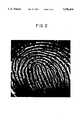
- FIG. 2is a negative image of a fingerprint that has been transferred to an image sensing device by the uneven surface image transfer apparatus of the present invention
- FIG. 3is an exploded view of the apparatus of FIG. 1 detailing the relative arrangement of the uneven surface image transfer apparatus of the present invention with other components;
- FIG. 4is a partial cross-sectional view of the apparatus of FIG. 1 illustrating the assembled arrangement of the uneven surface image transfer apparatus of the present invention with other components;
- FIG. 5is a top view of only the image transfer apparatus, taken along the line 5--5 of FIG. 4;
- FIG. 6is a bottom view of only the image transfer apparatus, taken along the line 6--6 of FIG. 4;
- FIG. 7is a cross-sectional view taken along the line 7--7 of FIG. 5;
- FIG. 8is a cross-sectional view taken along the line 8--8 of FIG. 7;
- FIG. 9is a cross-sectional view taken along the line 9--9 of FIG. 7;
- FIG. 10is a cross-sectional view taken along the line 10--10 of FIG. 7;
- FIG. 11is a side view of a propagation of light waves through the apparatus of FIG. 5 onto an image sensing device;
- FIG. 12is a front view of the propagation of light waves as shown in FIG. 11;
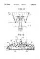
- FIG. 13is an uneven surface image transfer apparatus in accordance with a second embodiment of the present invention.
- a fingerprint reader apparatus 20as may be used with the uneven surface image transfer apparatus of the present invention.
- the illustrated fingerprint reader apparatus 20has particular advantages that are attributable to the ergonomic shape of the unit, as described in co-pending U.S. Application Serial No. UNASSIGNED to Merjanian, for ERGONOMIC FINGERPRINT READER APPARATUS, filed on Oct. 28, 1994, the disclosure of which is hereby incorporated by reference as though fully set forth herein.
- the particular housing for the image transfer apparatus of the present inventionis not critical to the present invention.
- the ergonomic apparatus 20may be connected by a tether 22 to a base unit 24 to comprise a fingerprint reading system 26.
- a hand 28has grasped the ergonomic reader 20 and has placed a digit 32 on a platen 130 (obscured in this Figure by the digit 32).
- the platenis one reflective surface of an optical plate 64 that comprises the uneven surface image transfer apparatus of the present invention.
- the platenserves as an image transfer surface upon which the image from the digit 32 is conveyed to an image sensing device.
- the image sensing deviceconverts the optical image from a top or presentation surface 31 of the platen 130 to an electronic signal for transmission through wires or optical cables (not shown) within the tether 22 to the base 24.
- informationmay be transferred from the base 24 to an external device, for example, a computer or modem, through a serial interface 40.
- a power port 41may be used to connect the system to an external source of power, if necessary.
- the print of every digit 32is comprised of raised ridges separated by sunken valleys.
- the patterns of the printare unique to every individual.
- the ridges of the fingerprintwill decouple near-surface electromagnetic fields at their contact points, thereby causing an evanescent wave surface effect to occur at the platen, that is, causing the rays at those points to be absorbed, scattered, or both. This severely attenuates the rays at those contact points and produces a wavefront of attenuated evanescent wave image rays (or an absence of evanescent wave image rays) for transfer to the image sensing device 168.
- the dark portions of the fingerprint imagerepresent the contact points of the ridges of the fingerprint of the individual's digit 32 with the presentation surface 31 of the platen 130. These contact points cause an evanescent wave surface effect to occur at the platen 130, and produce a wavefront of severely attenuated image rays for transfer to the image sensing device 168.
- the lighter portionsrepresent the locations of the valleys of the individual's digit at which points the evanescent wave has not been decoupled because no surface effect has occurred at the platen 130, and so any radiation injected into the optical plate 64 is transferred to the image sensing device 168 at these points without interference.
- veiling glarethat is, internal scattering that ultimately impinges on the image sensing device
- the contrast between the dark and light portionsmay be reduced somewhat; however, this mild reduction in contrast is tolerable by most image processing systems.
- the ergonomic reader 20has first and second hemispherical portions 58,60 that house an integrated optical system 62.
- the integrated optical system 62comprises in addition to the optical plate 64 having a platen 130 on one side thereof, a printed circuit board (PCB) 66 on the other side thereof, although other configurations are of course possible.
- the PCB 66includes the external image sensing device 168 upon which images from the platen 130 are conveyed and a complement of other electronic components 70A,B, . . . N.
- the first hemispherical portion 58has a generally planar surface 46 with an aperture 48 therethrough.
- the aperture 48is assembled in register with the platen 130 of the optical plate 64 to provide a window to the platen so that fingerprint data may be acquired by placing the digit 32 on the presentation surface 31 of the platen 130, as illustrated in FIG. 1. While the aperture 48 is illustrated as having a generally elliptical opening, the invention is not so limited. As previously noted, the housing for the uneven surface image transfer apparatus is not critical to the invention.
- Through-holes 74 in the PCB 66 and posts 76, extending from one side of the optical plate 64,permit assembly of the integrated optical system 62 as a unit.
- the posts 76have threaded apertures 77 (FIG. 7) to receive screws 77A to complete the assembly.
- a piece of structural foam adhesive tape 78is interposed between the assembly of the integrated optical system 62 and the first hemispherical portion 58 to seal the assembly into contact with the first hemispherical portion.
- the tape 78also serves as a gasket to block light, seal out dirt and grease, and otherwise isolate the reflective surfaces of the optical plate 64 from contact with the first hemispherical portion or other objects along the optical path that the evanescent wave image is conveyed. Isolation along the optical path is required as any contact with a reflective surface in the path will decouple portions of the evanescent wave image by absorbing light and causing scatter instead of reflection.
- At least one aperture 80is provided in the tape 78 to isolate reflective surfaces of a top surface 86 of the optical plate 64 along the optical path of the transferred image.
- an apertured surfacemay be placed in contact with a bottom surface 88, provided that the interface of the optical plate 64 with some other object is free of contact with the other object at points of total internal reflection (TIR) along the optical path.
- TIRtotal internal reflection
- the aperture 48 in the first hemispherical portionallows contact of the digit 32 with the presentation surface 31 to decouple the field in the vicinity of the ridges of the fingerprint, but not in the vicinity of the valleys, to prevent specular reflection at such contact points and remove radiation thereat.
- a negative image of the digit 32 on the presentation surface 31is created and transferred to the external image sensing device 168, as shown in FIG. 2.
- the second hemispherical portion 60is snap-fit into contact with the first hemispherical portion 58 to complete the assembly.
- Other electronicsfor example, circuitry related to fingerprint data compression, analysis, or both, or related to other electronic functions such as wireless communication, etc. may be housed within the second hemispherical portion 60.
- FIG. 4depicts the physical relationship among the assembled components, and in particular, the assembly of the integrated optical system 62 of FIG. 3.
- the printed circuit board 66 and optical plate 64 assemblyare secured in position by the tape 78 immediately below the planar surface 46.
- the platen 130is shown aligned with the aperture 48 so that a digit 32 placed on the presentation surface 31 of the platen 130 can provide input data to the image sensing device 168 mounted on the printed circuit board 66.
- the optical plate 64precisely converges a field of radiation from an external source 90 using an aspherical illuminating lens 128.
- the illuminating lens 128is an aspherical lens that nominally focusses the radiation from the source 90 at point between two totally internally reflecting (TIR) surfaces within the optical plate 64.
- the source 90is mounted within a slot 92 on the bottom surface 88 of the optical plate 64 such that its center line of radiation is in common with the center line of the illuminating lens 128 (see FIG. 6).
- the source 90has the form factor of a T-1 package, and preferably is a T-1 package light emitting diode (LED).
- the aspherical illuminating lens 128uniformly irradiates leading and trailing edges 94, 96 of the platen 130 by bending the light from the source 90 while efficiently coupling the radiation therefrom into the optical plate 64.
- the aspherical illuminating lens 128mildly converges the radiation from the source 90 into a cone that is nominally focussed at the aperture stop of an imaging lens 142, so that most of the light from the source 90 transfers to the image sensing device 168 as a wavefront of evanescent wave image rays.
- the light from the source 90is conveyed by the illumination lens 128 to the platen 130 at angles in excess of the critical angle according to Fresnel's laws of reflection.
- the radiation that is incident on the platen 130will then totally internally reflect (TIR) therefrom at each glass-to-air or plastic-to-air interface along the optical path and thereby propagate or transfer through the optical plate 64 to the imaging lens 142.
- TIRtotally internally reflect
- the critical angleis approximately forty-two degrees for acrylic plastic; however, TIR can be achieved at angles less than the critical angle by coating the surface with a reflective material such as aluminum or silver, for example.
- the evanescent wave image raysreflect at an angle equal to angle of incidence in accordance with Snell's Law, and is directed, according to the present invention, by changing the orientation or curvature of the reflecting surface.
- the evanescent wave image rayscontinue to reflect within the optical plate 64 until it is directed to the imaging lens 142, at which point it exits the optical plate 64 and is presented to the surface of the external image sensing device 168.
- a diffusing or apodizing surface 98may be interposed between the source 90 and the illuminating lens 128.
- TIRrequires an angle of incidence of the radiation source 90 to the planar presentation surface 31 that is typically in excess of forty-two degrees
- the image rays transferred to the external image sensing device 168would normally experience a high degree of geometric perspective distortion.
- a rectangular platenis imaged to the external imaging device 168, it appears in a keystone or trapezoidal shape because the sides are imaged to be non-parallel.
- each of the optical surfacesare used off-axis, that is, light is not nominally incident in a direction normal to their surfaces, but rather strikes a leading edge of the surface before the trailing edge.
- Such distortioncan be corrected by a compensating tilt in the image plane as taught in the aforementioned U.S. Pat. No.
- one or more toroidal TIR elementsare placed intermediate to the presentation surface 31 and the imaging lens 142 to reduce or eliminate geometric perspective distortion and astigmatism prior to transferring the image rays to the external image sensing device 168.
- the toroidal elements in conjunction with the off-axis imaging asphereinfluence the light path in a manner to make the image at the image sensing device 168 appear as though the source 90 irradiated the platen 130 in a nearly orthogonal direction, rather than at the critical angle that was actually used to introduce TIR. Further, the use of aspheric lenses 128 and 142 in place of simple spherical surfaces further contributes to the high-resolution, low distortion images that are transferred by the optical plate 64 to the external image sensing device 168.
- each of the described surfacesis positioned along the optical axis of the optical plate 64 so that reflected light from the leading and trailing edges 94, 96 of the platen 130 are incident upon each of the respective surfaces and transferred toward the external image sensing device 168 by TIR.
- the optical plate 64may comprise a clear, solid block of optical plastic, for example, acrylic, formed by an injection molding process, or may be a glass plate. In either case, the optical plate 64 is fabricated so as to provide surfaces and lenses for transferring image data from the platen 130 to the external image sensing device 168.
- the optical plate 64comprises the platen 130, and the aspheric illuminating and imaging lenses 128,142, respectively, for imaging a fingerprint from the platen 130 onto the external image sensing device 168 as light rays by refraction from the imaging lens 142. Integral with the optical plate 64 are reflecting surfaces between the platen 130 and the aspheric imaging lens, some of which are toroidal.
- the toroidal surfaceswork in combination with the aspheric imaging lens 142 to reduce or eliminate any geometric distortion or astigmatism in the image that is transferred to the image sensing device 168.
- the geometric distortionresults from the optical TIR angular perspective view of the platen at the image sensing device 168.
- the top surface 86 of the optical plate 64is shown.
- the top surface 86has ground and polished surfaces that comprise the platen 130 and first and second toroidal surfaces 136, 140.
- the toroidal surfaces 136, 140have optical power that is dominant in the axis of propagation to reduce or eliminate geometric distortion and astigmatism at the plane of the imaging device. However, this creates astigmatism within the optical plate 64, especially at the nominal stop plane of the off-axis aspheric imaging lens 142, which then has differential stop planes in the x- and y-axes.
- the second toroidal surface 140provides a narrow aperture in an axis transverse to the propagation of light, which is arbitrarily labeled the x-axis in this embodiment, and a wide aperture in an axis aligned with the propagation of light, which is arbitrarily labeled the y-axis.
- the second toroidal surface 140is formed as a rectangular surface, with the long axis oriented in the y-direction, and a relatively narrow surface in the x-direction.
- the second toroidal surface 140provides an aperture stop in the x-direction only and at an optimal astigmatic distance from the imaging lens 142, thereby stopping down or narrowing the cone of light rays that are incident on the imaging lens 142 in this axial direction.
- the narrowed conereduces the circle of confusion or blur in an image at the image sensing device 168 in this axial direction.
- the second toroidal surface 140is positioned relative to the top surface 86 within an angular recess 100 at the frustrum of a frustrotrapezoidal section 102 to receive light reflected from a second planar surface 138, described below.
- the frustrumpreferably has an aluminum or silver coating 103 to enhance the reflectivity of this surface.
- the x-direction aperture stop for the aspheric imaging lens 142is located on one side of the nominal focal point of the illuminating lens 128 whereas the y-direction aperture stop for the imaging lens 142 is displaced in space to the other side of this nominal focal point.
- FIG. 6shows the bottom surface 88 of the optical plate 64 through which radiation is provided and image data is extracted.
- the bottom surface 88includes a wall 104 that extends normally therefrom along one margin of the optical plate.
- the wall 104has the slot 92 therethrough for housing the source 90 at an angle sufficient to totally internally reflect radiant energy from the source off of the platen 130.
- a cavity 106Between the wall 104 and the illuminating lens 128 is a cavity 106 that permits radiation from the source 90 to shine on the illuminating lens 128.
- the walls of the cavity 106may define slots 108 for supporting the optional diffusing or apodizing surface 98.
- the filler 110On the other side of the illuminating lens 128 there is a filler 110 which prevents truncation of radiation from the source 90 between a bottommost portion of the illuminating lens 128 and the ostensible bottom plane of the optical plate 64.
- the fillerhas an unpolished tool surface 112 (FIG. 7) and is simply an extension of the optical material of the optical plate 64.
- first and second planar surfaces 134, 138are provided, in part, to steer evanescent wave image rays reflected from the platen 130 toward the aspheric imaging lens 142.
- the first planar surface 134is positioned on the bottom surface 88 so that reflected image rays from the leading and trailing edges 94, 96 of the platen 130 are incident thereupon.
- the second planar surface 138is formed as the frustrum of a frustroconical section 114, although the invention is not so limited.
- the frustroconical section 114positions the frustrum or second planar surface 138 so that the TIR evanescent wave image rays, reflected from the first toroidal surface 136, are incident thereupon.
- the second planar surface 138need only be formed to provide a wide aperture in the x-axis, and a narrow aperture in the y-axis to provide an aperture stop in a direction orthoganol to the aperture stop provided by the second toroidal surface 140, namely, in the y-direction only at an optimal astigmatic distance from the imaging lens 142, stopping down or narrowing the cone of light rays that are incident on the imaging lens 142 in this axial direction.
- the second planar surfacecould readily be formed as a rectangular surface, with the long axis oriented in the y-direction.
- the second planar surface 138, the second toroidal surface 140, and the aspheric imaging lens 142provide a split-axis aperture stop, stopping down or narrowing the cone of light rays incident on the imaging lens 142 in the x- and y-directions, at different points in space, thereby accommodating the astigmatism of the stop plane.
- the off-axis TIR design with geometric distortion-correcting toroidsintroduces an astigmatism in the optical system
- the x- and y-focal pointsdo not coincide in one plane within the optical plate 64.
- the stop of the systemis disjointed or split, and resolution, in terms of depth of focus, is enhanced by the aforementioned second planar surface 138 which is adapted to stop down the y-directed rays of light from the platen 130 at the y-focal point, and by the aforementioned second toroidal surface 140 which is adapted to stop down the x-directed rays of light from the platen 130 at the x-focal point, which is further along the direction of propagation of the light, that is, the y-direction.
- Image bluris therefore reduced or eliminated by accommodating stop-plane astigmatism which is otherwise introduced by the toroids 136, 140 and the off-axis aspheric lens 142, while providing a wide field of view of the platen 130.
- one of the toroidal elements and one of the planar elementsare used in combination to form the system aperture to control the f/number, the overall resolution, and stray light.
- the light path for image transfer through the optical plate 64commences with source 90 through illuminating lens 128 to the platen 130 where a digit 32 may be placed, and from the platen 130 to the first planar surface 134, then to the first toroidal surface 136 and then to the second planar surface 138, all by TIR. From the second planar surface 138, the evanescent wave image rays strike the second toroidal surface 140 which is backed by an aluminum coating because it is only about sixty percent TIR, and reflects therefrom to the imaging lens 142. From the imaging lens 142, the evanescent wave image rays are transferred to the external image sensing device 168. In shorthand, the optical path into and out of the optical plate 64 is: 90-128-130-134-136-138-140-142-168.
- the optical plate 64is mounted in spaced relation to the PCB 66 having the image sensing device 168 by the posts 76 and threaded apertures 77.
- a flange 116 on one of the posts 76may locate the imaging lens 142 relative to the image sensing device 168 when the optical plate 64 and PCB 66 are assembled.
- the flange 116may be received in a slot 69 in the image sensing device 168, which slot is typically provided so that the pins of the integrated device, for example, a charge coupled device chip, may be oriented with respect to the PCB 66.
- the flangewould therefore assist in locating the optical plate 64 over the PCB 66.
- the integrated optical system 62is held together by screws 77A.
- FIG. 7is not intended to be a scale drawing. It is seen that the source 90 in the slot 92 irradiates the aspheric illuminating lens 128 at a preselected angle so that the light from the source 90 is distributed across the platen 130 by the illuminating lens 128 at the critical angle or greater. In FIG. 8, the filler 110 and unpolished surface 112 are shown.
- the light from the source 90is not truncated, but rather floods the extent of the platen 130, from its leading to trailing edges 94,96.
- the geometry of the first toroidal surface 136is shown as having a curve of one radius in the y-axis, and, in FIG. 9, a curve of another radius in the x-axis.
- the geometry of the second toroidal surface 140is shown in the orthoganol views of FIGS. 7 and 10.
- the second toroidal surface 140has its long axis oriented in the y-direction (FIG. 7), and has its relatively narrow surface in the x-direction (FIG. 10).
- FIG. 7also shows the relative alignment of the aspheric imaging lens 142 and the image sensing device 168.
- the evanescent wave image rays including digit data or fingerprint informationare transferred by the aspheric imaging lens 142 uniformly across the top surface of the image sensing device 168. Further, the aspheric imaging lens 142 is positioned so that its aperture stop is located at the nominal focal point of the illuminating lens 128. In this way, a high percentage of the radiation can be delivered the external image sensing device 168.
- the optically active regionthat is the portion of the optical plate 64 through which the evanescent wave image rays travel, is approximately 0.75" W ⁇ 0.31" H ⁇ 2.00" L.
- the radiation source mountingthe wall 122 and the slot 104
- the external image sensing device 168 mounted on the PCB 66the overall dimensions increase to approximately 0.75" W ⁇ 0.75" H ⁇ 2.50" L.
- the propagation or transfer of the evanescent wave imageis detailed in the y-direction, that is, in the direction of the propagation of light, with the optical plate 64 shown in phantom.
- the source 90emits radiation in a generally diverging pattern which is converted to a mildly convergent beam by the aspherical illuminating lens 128.
- the illuminating lens 128spreads the radiant energy from the source across the platen 130 from its leading edge 94 to its trailing edge 96 so that evanescent wave image data presented to the platen 130 can be transferred to the image sensing device 168.
- TIRthe image data is reflected from the platen 130 to the surfaces 134, 136, 138, 140 and through the imaging lens 142.
- the image waveconverges as it travels toward the second planar surface 138, and before reaching the second toroidal surface 140, the image wave converges at the nominal focal point FP of the illuminating lens 128. Thereafter, the leading and trailing edges of the image wave are inverted, and so the data from the leading edge 94 of the platen strikes the second toroidal surface 140 at that surface's trailing edge, and vice versa. The reversed image then exits the optical plate 64 through the imaging lens 142 and is transferred to the external image sensing device 168.
- FIG. 12the same propagation of the evanescent wave image is illustrated, this time from a front view, that is, showing the x-direction which is transverse to the direction of the propagation of light in the optical plate 64.
- the evanescent wave imageconverges at FP between the second planar surface 138 and the second toroidal surface 140.
- the overall magnification or fan in these directionsis preferably configured to be the same. For example, a construction can be achieved having nearly matching magnifications, M, in the x- and y-axes (FIGS. 11 and 12).
- FIG. 13a second embodiment of the uneven surface detection apparatus is shown in which features common to the first embodiment are given corresponding reference numerals. Otherwise than as specifically described below, this alternative embodiment shares the inventive lens arrangement adapted to reduce or eliminate geometric perspective distortion and astigmatism within the optical plate 64, and operates using the source 90 as described above. However, for certain database and security applications, it may be desirable to scan information to supplement fingerprint data, or simply other information altogether such as bar code or other data.
- the optical system 62' of FIG. 13includes in addition to the features of the optical plate 64, a source 200 mounted on the PCB 66' so as to irradiate the optical plate 64' nearly or substantially normal to the bottom surface 88.
- the light radiated by the source 200enters the optical plate 64' at A, beneath the presentation surface 31, and passes therethrough to an opposite margin B, at which point it is refracted outward at an angle somewhat skewed from a line normal to the top surface 86 of the optical plate 64'.
- the light irradiated from the source 200may then impinge upon an object 202 located generally above point B, but not necessarily in contact with or parallel to the presentation surface 31.
- the object 202may contain a bar code BC or other uneven surface for transferring to an image sensing device 204 (or image sensing device 168).
- the image sensing device 204may be a linear CCD chip, as commonly used for bar code scanning in point-of-sale and industrial applications.
- the image sensing device 168 of the first embodimentwhich is preferably a CCD chip including an image area sensor (IAR)
- IARimage area sensor
- the image sensing device 168 of the first embodimentcan be used as a limited-field or linear CCD by prematurely terminating the area scan pattern with a scan reset pulse so that only a few lines in the CCD array are utilized. In this manner, only that portion of the CCD scan area which receives the transferred image from the object 202 is utilized.
- the complement of other electronic components 70A,B, . . . N mounted on the PCB 66'may include circuitry to reset the scan cycle of the image sensing device 168 under control of such circuitry as understood by persons skilled in the art, and may further include circuitry to switch the mode of operation between that described for the first and second embodiments.
- the optical plate 64'includes a linear prismatic element 206 in the vicinity of the trailing edge 96 of the platen 130. A portion of the light reflected from the object 202 enters the optical plate 64' through the refractive prismatic element 206. The light is then reflectively transferred in a manner as previously described to the image sensing device.
- the linear prismatic element 206may be integrally formed on the optical plate 64', and, in any event, is mounted or formed at an angle chosen to frustrate TIR, in other words, at an angle that is refractively transmissive.
- Scanning of two-dimensional bar codescan be facilitated by providing a slot (not shown) for controlled motion of objects 202 such as credit cards.
- This slotmay be integral to the presentation surface 31, and in particular, can be formed as part of a finger-stop or tactile feedback means which may also serve as an indicator to the operator of the location of his or her digit 32 on the platen 130.
- a fingerprintcan be captured at a location remote to the optical plate 64' for later transfer to the image sensing device by use of a thermally activated sheet of paper.
- the thermally activated paperresponds, for example, to an individual's body temperature by recording a fingerprint image thereon.
- the imagecan then be converted to a digital format by reflecting the fingerprint image data from the thermal paper (which serves as the object 202 in this exemplary application) using the uneven surface detection apparatus of FIG. 13.
- the resolution performancecan be enhanced by including a device for shuttering the external image sensing device 168,204 between open and closed positions.
- the object whose image is being transferredis captured over an abbreviated time period which reduces the exposure time of the image sensing device and thereby limits the effects of any motion of the object which might otherwise blur the transferred image.
- the optical system 62'may include a strobing device for intermittently illuminating the platen, and perhaps an actuator for actuating the image sensing device and causing same to capture either evanescent wave or bar code BC image data from the platen 130 or the prismatic element 206.
- the sourcemay be operated at a higher level of emission to deliver a nominally equivalent amount of energy in a shorter period of time without overheating or being damaged.
- the actuatorcauses the external image sensing device to capture images in synchronization with the intermittent illuminations of the platen or prismatic surface. Either the shuttering or the strobing or both can be accomplished by conventional mechanical or electronic devices.
- the surface figure and irregularity of the lensesshould be within 20 fringes.
- the scratchshould be no greater than 60 microns wide and the dig no greater than 40 microns wide, per surface.
- the axis of each lens or molding tool insertshould be ground, polished, or both to within 0°1'30".
- the lens centrationshould be ⁇ 0.002" on the toroidal surfaces and ⁇ 0.005" on the other lens surfaces.
- the image sensing device 168may be a conventional CMOS CCD device. It is preferred that the image area sensor (IAR) be able to resolve 500 dots per inch (DPI).
- a conventional CCD chiphas 510 ⁇ 494 pixels, each of which is digitized to an 8 bit value.
- 500 DPIis the baseline resolution used by several fingerprint feature detection systems, including the Federal Bureau of Investigation's fingerprint identification system and in a system disclosed in U.S. application Ser. No. 08/036,845 to Shen, filed Mar. 25, 1993, for METHOD AND SYSTEM FOR DETECTING FEATURES OF FINGERPRINT IN GRAY LEVEL IMAGE, assigned to Cogent Systems, Inc.
- the digitized signalmay be filtered to (a) remove background noise, and (b) perform edge enhancement.
- the edge enhancement processsharpens the image and fills in any erroneous gaps in the ridge of a fingerprint.
- This signalis then ported to a fingerprint feature detection system such as either of the aforementioned systems.
- This signalis from 16K to 40K, depending on the particular application. For example, if the fingerprint information is transmitted by hard wire, then a 40K signal can readily be transmitted.
- the digital processormay further include digital compression to reduce the information down to 16K so that it may be transmitted by a wireless link, as understood by persons skilled in the art.
- Any acquired fingerprint image datais stored in less than about 1K of memory, for example, in a bar code such as by Symbol, in semiconductor memory (RAM, DRAM, SRAM, EPROM, PROM, ROM), or on optical or magnetic media (CD ROM, Laserdisk, Minidisk, hard disk, or floppy disk), as understood by those skilled in the art.
- a bar codesuch as by Symbol, in semiconductor memory (RAM, DRAM, SRAM, EPROM, PROM, ROM), or on optical or magnetic media (CD ROM, Laserdisk, Minidisk, hard disk, or floppy disk), as understood by those skilled in the art.
- the source 90emits a small range of wavelengths centered around 565 nm (which appear green to the naked eye), preferably in the range of 550 to 600 nm. While other wavelengths could be used as well, these preferred wavelengths are selected because they provide a sharp image at the image sensing device 168 and optimal contrast for flesh-tone fingerprints.
- the center wavelength output by the sourcehas been chosen to be at the peak sensitivity of CCD's so that the image sensing device is made sensitive. This center wavelength is outside of the range of wavelengths centered about 565 nm.
- optical plate 64efficiently reflects light to the image sensing device, some sensitivity can be sacrificed in the present design in favor of image quality, at the discretion of the optical design engineer charged with striking a balance between these conflicting design criteria.
- the reflective surfaces intermediate the platen 130 and the image sensing device 168are selected to optimize the optical design by minimizing geometric distortion at the selected source output wavelength.
- uneven surfacerefers to a surface that is uneven in the physical sense of an irregular surface contour, or uneven in the optical sense of contrasting surfaces, and in particular, juxtaposed black and white images such as the bar code BC.
- fingerprintrefers to the ridge and groove patterns found on the digits of either hand, including the pinky, ring, middle, and index fingers as well as the thumb.
- image processing systemrefers to the compression, analysis, and matching routines that may be used in conjunction with the integrated optical system 62 of the present invention.
- plateas used herein embraces the prismatic element 206, notwithstanding any previous discussions in which the terms are used in the alternative.
Landscapes
- Physics & Mathematics (AREA)
- General Physics & Mathematics (AREA)
- Optics & Photonics (AREA)
- Engineering & Computer Science (AREA)
- Human Computer Interaction (AREA)
- Multimedia (AREA)
- Theoretical Computer Science (AREA)
- Image Input (AREA)
- Lenses (AREA)
- Solid State Image Pick-Up Elements (AREA)
Abstract
Description
Claims (31)
Priority Applications (7)
| Application Number | Priority Date | Filing Date | Title |
|---|---|---|---|
| US08/332,548US5596454A (en) | 1994-10-28 | 1994-10-28 | Uneven surface image transfer apparatus |
| CN95197922ACN1209881A (en) | 1994-10-28 | 1995-10-27 | Uneven surface image transfer apparatus |
| PCT/US1995/014373WO1996013742A1 (en) | 1994-10-28 | 1995-10-27 | Uneven surface image transfer apparatus |
| JP8514866AJPH11509639A (en) | 1994-10-28 | 1995-10-27 | Rough surface image transfer device |
| CA002203924ACA2203924A1 (en) | 1994-10-28 | 1995-10-27 | Uneven surface image transfer apparatus |
| EP95941361AEP0842448A1 (en) | 1994-10-28 | 1995-10-27 | Uneven surface image transfer apparatus |
| AU42809/96AAU4280996A (en) | 1994-10-28 | 1995-10-27 | Uneven surface image transfer apparatus |
Applications Claiming Priority (1)
| Application Number | Priority Date | Filing Date | Title |
|---|---|---|---|
| US08/332,548US5596454A (en) | 1994-10-28 | 1994-10-28 | Uneven surface image transfer apparatus |
Publications (1)
| Publication Number | Publication Date |
|---|---|
| US5596454Atrue US5596454A (en) | 1997-01-21 |
Family
ID=23298736
Family Applications (1)
| Application Number | Title | Priority Date | Filing Date |
|---|---|---|---|
| US08/332,548Expired - Fee RelatedUS5596454A (en) | 1994-10-28 | 1994-10-28 | Uneven surface image transfer apparatus |
Country Status (7)
| Country | Link |
|---|---|
| US (1) | US5596454A (en) |
| EP (1) | EP0842448A1 (en) |
| JP (1) | JPH11509639A (en) |
| CN (1) | CN1209881A (en) |
| AU (1) | AU4280996A (en) |
| CA (1) | CA2203924A1 (en) |
| WO (1) | WO1996013742A1 (en) |
Cited By (62)
| Publication number | Priority date | Publication date | Assignee | Title |
|---|---|---|---|---|
| WO1998047096A1 (en)* | 1997-04-17 | 1998-10-22 | Cross Check Corporation | Hand-held fingerprint recognition and transmission device |
| US5926318A (en)* | 1998-04-06 | 1999-07-20 | Optimize Incorporated | Biocular viewing system with intermediate image planes for an electronic display device |
| WO1999041631A1 (en)* | 1998-02-12 | 1999-08-19 | Electro-Optical Systems Corporation | Optical fingerprint reader |
| WO1999056236A1 (en)* | 1998-04-28 | 1999-11-04 | Cross Match Technologies, Inc. | Individualized fingerprint scanner |
| US5991431A (en)* | 1996-02-12 | 1999-11-23 | Dew Engineering And Development Limited | Mouse adapted to scan biometric data |
| US5995630A (en)* | 1996-03-07 | 1999-11-30 | Dew Engineering And Development Limited | Biometric input with encryption |
| WO1999063476A1 (en)* | 1998-06-02 | 1999-12-09 | Digital Persona, Inc. | Method and apparatus for scanning a fingerprint using a linear sensor |
| US6122394A (en)* | 1996-05-01 | 2000-09-19 | Xros, Inc. | Compact, simple, 2D raster, image-building fingerprint scanner |
| US6127674A (en)* | 1997-09-01 | 2000-10-03 | Fujitsu Limited | Uneven-surface data detection apparatus |
| US6188781B1 (en) | 1998-07-28 | 2001-02-13 | Digital Persona, Inc. | Method and apparatus for illuminating a fingerprint through side illumination of a platen |
| WO2001018741A1 (en)* | 1999-09-08 | 2001-03-15 | Digital Persona, Inc. | A thin prism fingerprint imager system |
| US6219186B1 (en) | 1998-04-06 | 2001-04-17 | Optimize Incorporated | Compact biocular viewing system for an electronic display |
| US6263090B1 (en) | 1997-05-19 | 2001-07-17 | Cross Match Technologies, Inc. | Code reader fingerprint scanner |
| US6272562B1 (en) | 1999-05-28 | 2001-08-07 | Cross Match Technologies, Inc. | Access control unit interface |
| US6289114B1 (en)* | 1996-06-14 | 2001-09-11 | Thomson-Csf | Fingerprint-reading system |
| US6414749B1 (en) | 1998-12-24 | 2002-07-02 | Mitsubishi Denki Kabushiki Kaisha | Uneven-pattern reading apparatus |
| US20020110266A1 (en)* | 1998-11-12 | 2002-08-15 | Teng Harry H. | High contrast, low distortion optical acquisition system for image capturing |
| US20020131624A1 (en)* | 2000-08-11 | 2002-09-19 | Yury Shapiro | Fingerprint imaging device with fake finger detection |
| US20020163601A1 (en)* | 2001-05-04 | 2002-11-07 | Min Kyoung Il | Liquid crystal display and fingerprint capture panel |
| US20030016427A1 (en)* | 2001-04-26 | 2003-01-23 | Arnold Joe F. | Silicon rubber surfaces for biometric print TIR prisms |
| US20030053228A1 (en)* | 2001-09-17 | 2003-03-20 | Lee Jong Ik | Optical fingerprint acquisition apparatus |
| US20030091219A1 (en)* | 1999-08-19 | 2003-05-15 | Martinez Chris J. | Method and apparatus for rolled fingerprint capture |
| US20030123716A1 (en)* | 1999-08-09 | 2003-07-03 | Cross Match Technologies, Inc. | System and method for sending a packet with position address and line scan data over an interface cable |
| US20030128240A1 (en)* | 1999-08-09 | 2003-07-10 | Martinez Chris J. | Method, system, and computer program product for a GUI to fingerprint scanner interface |
| US20030133103A1 (en)* | 2002-01-17 | 2003-07-17 | Arnold Joseph F. | Systems and methods for illuminating a platen in a print scanner |
| US20030133143A1 (en)* | 2002-01-17 | 2003-07-17 | Cross Match Technology, Inc. | Biometric imaging system and method |
| US20030149343A1 (en)* | 2001-09-26 | 2003-08-07 | Cross Match Technologies, Inc. | Biometric based facility security |
| US20030200446A1 (en)* | 2002-04-19 | 2003-10-23 | Cross Match Technologies, Inc. | System and methods for access control utilizing two factors to control access |
| US20030197593A1 (en)* | 2002-04-19 | 2003-10-23 | Cross Match Technologies, Inc. | Systems and methods utilizing biometric data |
| US20030206287A1 (en)* | 2002-01-17 | 2003-11-06 | Cross Match Technologies, Inc. | Light wedge for illuminating a platen in a print scanner |
| US20040016811A1 (en)* | 2002-04-19 | 2004-01-29 | Cross Match Technologies, Inc. | Mobile handheld code reader and print scanner system and method |
| US6687391B1 (en) | 1999-10-22 | 2004-02-03 | Cross Match Technologies, Inc. | Adjustable, rotatable finger guide in a tenprint scanner with movable prism platen |
| US6744910B1 (en) | 1999-06-25 | 2004-06-01 | Cross Match Technologies, Inc. | Hand-held fingerprint scanner with on-board image normalization data storage |
| US20040109590A1 (en)* | 2002-08-02 | 2004-06-10 | Cannon Gregory L. | System and method for counting ridges in a captured print image |
| US20040156555A1 (en)* | 1999-08-09 | 2004-08-12 | Cross Match Technologies, Inc. | Calibration and correction in a fingerprint scanner |
| US20040170303A1 (en)* | 2003-02-28 | 2004-09-02 | Cross Match Technology, Inc. | Dynamic image adaption method for adjusting the quality of digital prints |
| WO2004097715A1 (en)* | 2003-05-01 | 2004-11-11 | Novo Nordisk A/S | An optical system |
| US20050047631A1 (en)* | 2003-08-26 | 2005-03-03 | Cross Match Technologies, Inc. | Method and apparatus for rolled fingerprint image capture with variable blending |
| US6870946B1 (en) | 1998-08-06 | 2005-03-22 | Secugen Corporation | Compact optical fingerprint capturing and recognition system |
| US20050069182A1 (en)* | 2003-09-30 | 2005-03-31 | Schneider John K. | Finger scanner and method of scanning a finger |
| US6886104B1 (en) | 1999-06-25 | 2005-04-26 | Cross Match Technologies | Rechargeable mobile hand-held fingerprint scanner with a data and power communication interface |
| US6912300B1 (en)* | 1999-08-20 | 2005-06-28 | Mitsubishi Denki Kabushiki Kaisha | Irregular pattern reader |
| US20050157914A1 (en)* | 2002-08-21 | 2005-07-21 | Jee-Hoon Kim | TFT sensor having improved imaging surface |
| US6928195B2 (en) | 2000-12-18 | 2005-08-09 | Cross Match Technologies, Inc. | Palm scanner using a programmable nutating mirror for increased resolution |
| US6956608B1 (en) | 2000-08-11 | 2005-10-18 | Identix Incorporated | Fingerprint imaging device including an optical plate having microreflectors |
| US20050231576A1 (en)* | 2001-06-22 | 2005-10-20 | Lee David L | Color reproduction process |
| US6983062B2 (en) | 2000-08-18 | 2006-01-03 | Cross Match Technologies, Inc. | Fingerprint scanner auto-capture system and method |
| US7162060B1 (en) | 1999-08-09 | 2007-01-09 | Cross Match Technologies | Method, system, and computer program product for control of platen movement during a live scan |
| FR2890208A1 (en)* | 2005-08-30 | 2007-03-02 | Chuan Liang Ind Co Ltd | Fingerprint identification assembly for use in e.g. cellular phone, has light source illuminating fingerprint, where illuminated fingerprint is re-illuminated to sensor by multiple reflective surfaces |
| US20070112525A1 (en)* | 2005-11-16 | 2007-05-17 | Songtao Li | System and device for image-based biological data quantification |
| US20070209832A1 (en)* | 2006-03-09 | 2007-09-13 | Shelby Ball | Gaskets for protecting fingerprint readers from electrostatic discharge surges |
| US7277562B2 (en) | 2003-08-01 | 2007-10-02 | Cross Match Technologies, Inc. | Biometric imaging capture system and method |
| US20080273771A1 (en)* | 2007-05-01 | 2008-11-06 | Ming Hsieh | Apparatus for capturing a high quality image of a moist finger |
| US20090153293A1 (en)* | 2007-12-14 | 2009-06-18 | Chi Mei Communication Systems, Inc. | System and method for controlling access to a handheld device by validating fingerprints |
| US20090206243A1 (en)* | 2008-02-11 | 2009-08-20 | Texmag Gmbh Vertriebsgesellschaft | Image Capturing System and Method for the Analysis of Image Data |
| US20090208070A1 (en)* | 2008-02-14 | 2009-08-20 | Sagem Securite | Device for acquiring images of patterns formed by furrows in the skin of fingers or the palm of the hand |
| US20090268988A1 (en)* | 2002-02-14 | 2009-10-29 | Cogent Systems, Inc. | Method and apparatus for two dimensional image processing |
| US20100027852A1 (en)* | 2004-11-12 | 2010-02-04 | Ming Hsieh | System and Method for Fast Biometric Pattern Matching |
| US20120087555A1 (en)* | 2009-06-16 | 2012-04-12 | Morpho | Imaging device having a prismatic element |
| US20120146948A1 (en)* | 2010-12-13 | 2012-06-14 | Sae Magnetics (H.K.) Ltd. | Optical Navigation Module and Mobile Electronic Appliance Using Optical Navigation Module |
| US20120188385A1 (en)* | 2009-09-30 | 2012-07-26 | Sharp Kabushiki Kaisha | Optical pointing device and electronic equipment provided with the same, and light-guide and light-guiding method |
| US8683562B2 (en) | 2011-02-03 | 2014-03-25 | Imprivata, Inc. | Secure authentication using one-time passwords |
Families Citing this family (9)
| Publication number | Priority date | Publication date | Assignee | Title |
|---|---|---|---|---|
| US6259108B1 (en)* | 1998-10-09 | 2001-07-10 | Kinetic Sciences Inc. | Fingerprint image optical input apparatus |
| WO2003095766A1 (en)* | 2002-05-08 | 2003-11-20 | Kingyee Chan | Sidewall of swimming pool which matching with stand and method thereof |
| US7426020B2 (en) | 2003-06-17 | 2008-09-16 | Cross Match Technologies, Inc. | System for print imaging with prism illumination optics |
| US6954261B2 (en)* | 2003-06-17 | 2005-10-11 | Cross Match Technologies, Inc. | System and method for illuminating a platen in a live scanner and producing high-contrast print images |
| FR2859804B1 (en)* | 2003-09-12 | 2006-01-06 | Sagem | OPTICAL DEVICE FOR FORMING AN IMAGE OF DIGITAL IMPRESSIONS |
| US7063261B2 (en)* | 2004-07-23 | 2006-06-20 | Symbol Technologies, Inc. | Electro-optical reader with improved laser intensity modulation over extended working range |
| US8411916B2 (en) | 2007-06-11 | 2013-04-02 | 3M Cogent, Inc. | Bio-reader device with ticket identification |
| DE102010010328A1 (en)* | 2010-03-04 | 2011-09-29 | Jos. Schneider Optische Werke Gmbh | Planar imaging system |
| JP7241684B2 (en)* | 2016-10-25 | 2023-03-17 | トリナミクス ゲゼルシャフト ミット ベシュレンクテル ハフツング | detector for optical detection of at least one object |
Citations (18)
| Publication number | Priority date | Publication date | Assignee | Title |
|---|---|---|---|---|
| US3865488A (en)* | 1973-11-30 | 1975-02-11 | Rca Corp | Fingerprint display system utilizing a stored fingerprint |
| US3975711A (en)* | 1974-08-30 | 1976-08-17 | Sperry Rand Corporation | Real time fingerprint recording terminal |
| US4120585A (en)* | 1976-11-19 | 1978-10-17 | Calspan Corporation | Fingerprint identification system using a pliable optical prism |
| US4455083A (en)* | 1981-08-24 | 1984-06-19 | Elmes Paul B | Method and apparatus for fingerprint verification of identity |
| US4684802A (en)* | 1986-02-18 | 1987-08-04 | International Business Machines Corporation | Elliptical finger press scanner with rotating light source |
| US4728186A (en)* | 1985-03-03 | 1988-03-01 | Fujitsu Limited | Uneven-surface data detection apparatus |
| US4783167A (en)* | 1987-05-05 | 1988-11-08 | Fingermatrix, Inc. | Finger imaging apparatus using curved platen |
| US4784484A (en)* | 1985-05-02 | 1988-11-15 | Jydsk Telefon A/S | Method and apparatus for automatic scanning of fingerprints |
| US4785171A (en)* | 1987-01-15 | 1988-11-15 | Fingerprint Technology, Inc. | Fingerprint acquisition system with a fiber optic block |
| US4924085A (en)* | 1988-06-23 | 1990-05-08 | Fujitsu Limited | Uneven-surface data detection apparatus |
| US5067162A (en)* | 1986-06-30 | 1991-11-19 | Identix Incorporated | Method and apparatus for verifying identity using image correlation |
| US5088321A (en)* | 1989-11-02 | 1992-02-18 | Sumitomo Rubber Industries, Ltd. | Apparatus and method for observing the ground contact patch of a tire |
| US5088817A (en)* | 1988-11-25 | 1992-02-18 | Fujitsu Ltd | Biological object detection apparatus |
| US5109428A (en)* | 1988-12-06 | 1992-04-28 | Fujitsu Ltd | Minutia data extraction in fingerprint identification |
| US5146102A (en)* | 1990-02-22 | 1992-09-08 | Kabushiki Kaisha Toshiba | Fingerprint image input apparatus including a cylindrical lens |
| US5177802A (en)* | 1990-03-07 | 1993-01-05 | Sharp Kabushiki Kaisha | Fingerprint input apparatus |
| US5187748A (en)* | 1990-07-21 | 1993-02-16 | Goldstar, Inc. | Optical apparatus for fingerprint identification system |
| US5241606A (en)* | 1990-10-11 | 1993-08-31 | Matsushita Electric Industrial Co., Ltd. | Person identification apparatus |
Family Cites Families (2)
| Publication number | Priority date | Publication date | Assignee | Title |
|---|---|---|---|---|
| EP0308162A3 (en)* | 1987-09-15 | 1990-06-06 | Identix Incorporated | Optical system for fingerprint imaging |
| EP0359554B1 (en)* | 1988-09-16 | 1994-11-17 | Fujitsu Limited | Biological object detecting system and fingerprint collating system employing same |
- 1994
- 1994-10-28USUS08/332,548patent/US5596454A/ennot_activeExpired - Fee Related
- 1995
- 1995-10-27CNCN95197922Apatent/CN1209881A/enactivePending
- 1995-10-27EPEP95941361Apatent/EP0842448A1/ennot_activeWithdrawn
- 1995-10-27JPJP8514866Apatent/JPH11509639A/enactivePending
- 1995-10-27CACA002203924Apatent/CA2203924A1/ennot_activeAbandoned
- 1995-10-27AUAU42809/96Apatent/AU4280996A/ennot_activeAbandoned
- 1995-10-27WOPCT/US1995/014373patent/WO1996013742A1/ennot_activeApplication Discontinuation
Patent Citations (18)
| Publication number | Priority date | Publication date | Assignee | Title |
|---|---|---|---|---|
| US3865488A (en)* | 1973-11-30 | 1975-02-11 | Rca Corp | Fingerprint display system utilizing a stored fingerprint |
| US3975711A (en)* | 1974-08-30 | 1976-08-17 | Sperry Rand Corporation | Real time fingerprint recording terminal |
| US4120585A (en)* | 1976-11-19 | 1978-10-17 | Calspan Corporation | Fingerprint identification system using a pliable optical prism |
| US4455083A (en)* | 1981-08-24 | 1984-06-19 | Elmes Paul B | Method and apparatus for fingerprint verification of identity |
| US4728186A (en)* | 1985-03-03 | 1988-03-01 | Fujitsu Limited | Uneven-surface data detection apparatus |
| US4784484A (en)* | 1985-05-02 | 1988-11-15 | Jydsk Telefon A/S | Method and apparatus for automatic scanning of fingerprints |
| US4684802A (en)* | 1986-02-18 | 1987-08-04 | International Business Machines Corporation | Elliptical finger press scanner with rotating light source |
| US5067162A (en)* | 1986-06-30 | 1991-11-19 | Identix Incorporated | Method and apparatus for verifying identity using image correlation |
| US4785171A (en)* | 1987-01-15 | 1988-11-15 | Fingerprint Technology, Inc. | Fingerprint acquisition system with a fiber optic block |
| US4783167A (en)* | 1987-05-05 | 1988-11-08 | Fingermatrix, Inc. | Finger imaging apparatus using curved platen |
| US4924085A (en)* | 1988-06-23 | 1990-05-08 | Fujitsu Limited | Uneven-surface data detection apparatus |
| US5088817A (en)* | 1988-11-25 | 1992-02-18 | Fujitsu Ltd | Biological object detection apparatus |
| US5109428A (en)* | 1988-12-06 | 1992-04-28 | Fujitsu Ltd | Minutia data extraction in fingerprint identification |
| US5088321A (en)* | 1989-11-02 | 1992-02-18 | Sumitomo Rubber Industries, Ltd. | Apparatus and method for observing the ground contact patch of a tire |
| US5146102A (en)* | 1990-02-22 | 1992-09-08 | Kabushiki Kaisha Toshiba | Fingerprint image input apparatus including a cylindrical lens |
| US5177802A (en)* | 1990-03-07 | 1993-01-05 | Sharp Kabushiki Kaisha | Fingerprint input apparatus |
| US5187748A (en)* | 1990-07-21 | 1993-02-16 | Goldstar, Inc. | Optical apparatus for fingerprint identification system |
| US5241606A (en)* | 1990-10-11 | 1993-08-31 | Matsushita Electric Industrial Co., Ltd. | Person identification apparatus |
Cited By (115)
| Publication number | Priority date | Publication date | Assignee | Title |
|---|---|---|---|---|
| US5991431A (en)* | 1996-02-12 | 1999-11-23 | Dew Engineering And Development Limited | Mouse adapted to scan biometric data |
| US5995630A (en)* | 1996-03-07 | 1999-11-30 | Dew Engineering And Development Limited | Biometric input with encryption |
| US6122394A (en)* | 1996-05-01 | 2000-09-19 | Xros, Inc. | Compact, simple, 2D raster, image-building fingerprint scanner |
| US6289114B1 (en)* | 1996-06-14 | 2001-09-11 | Thomson-Csf | Fingerprint-reading system |
| US6459804B2 (en) | 1996-06-14 | 2002-10-01 | Thomson-Csf | Fingerprint-reading system |
| EP1501039A1 (en)* | 1997-04-17 | 2005-01-26 | Cross Match Technologies, Inc. | Hand-held fingerprint recognition and transmission device |
| WO1998047096A1 (en)* | 1997-04-17 | 1998-10-22 | Cross Check Corporation | Hand-held fingerprint recognition and transmission device |
| US6111977A (en)* | 1997-04-17 | 2000-08-29 | Cross Match Technologies, Inc. | Hand-held fingerprint recognition and transmission device |
| US6263090B1 (en) | 1997-05-19 | 2001-07-17 | Cross Match Technologies, Inc. | Code reader fingerprint scanner |
| US6127674A (en)* | 1997-09-01 | 2000-10-03 | Fujitsu Limited | Uneven-surface data detection apparatus |
| WO1999041631A1 (en)* | 1998-02-12 | 1999-08-19 | Electro-Optical Systems Corporation | Optical fingerprint reader |
| US6008939A (en)* | 1998-04-06 | 1999-12-28 | Optimize Incorporated | Method of color correction in a color video display system |
| US6219186B1 (en) | 1998-04-06 | 2001-04-17 | Optimize Incorporated | Compact biocular viewing system for an electronic display |
| US6040946A (en)* | 1998-04-06 | 2000-03-21 | Optimize Incorporated | Color superposition and mixing of light beams for a video display system |
| US5926318A (en)* | 1998-04-06 | 1999-07-20 | Optimize Incorporated | Biocular viewing system with intermediate image planes for an electronic display device |
| US6178255B1 (en) | 1998-04-28 | 2001-01-23 | Cross Match Technologies, Inc. | Individualized fingerprint scanner |
| US6628813B2 (en) | 1998-04-28 | 2003-09-30 | Cross Match Technologies, Inc. | Individualized fingerprint scanner |
| US20050100196A1 (en)* | 1998-04-28 | 2005-05-12 | Cross Match Technologies Inc. | Methods for capturing fingerprint images using a moving platen |
| WO1999056236A1 (en)* | 1998-04-28 | 1999-11-04 | Cross Match Technologies, Inc. | Individualized fingerprint scanner |
| US7103201B2 (en) | 1998-04-28 | 2006-09-05 | Cross Match Technologies, Inc. | Methods for capturing fingerprint images using a moving platen |
| US6282303B1 (en) | 1998-06-02 | 2001-08-28 | Digital Persona, Inc. | Method and apparatus for scanning a fingerprint using a linear sensor within a cursor control device |
| WO1999063476A1 (en)* | 1998-06-02 | 1999-12-09 | Digital Persona, Inc. | Method and apparatus for scanning a fingerprint using a linear sensor |
| US6324310B1 (en)* | 1998-06-02 | 2001-11-27 | Digital Persona, Inc. | Method and apparatus for scanning a fingerprint using a linear sensor |
| US6188781B1 (en) | 1998-07-28 | 2001-02-13 | Digital Persona, Inc. | Method and apparatus for illuminating a fingerprint through side illumination of a platen |
| US6870946B1 (en) | 1998-08-06 | 2005-03-22 | Secugen Corporation | Compact optical fingerprint capturing and recognition system |
| US6917695B2 (en) | 1998-11-12 | 2005-07-12 | Secugen Corporation | High contrast, low distortion optical acquisition system for image capturing |
| US20020110266A1 (en)* | 1998-11-12 | 2002-08-15 | Teng Harry H. | High contrast, low distortion optical acquisition system for image capturing |
| US6414749B1 (en) | 1998-12-24 | 2002-07-02 | Mitsubishi Denki Kabushiki Kaisha | Uneven-pattern reading apparatus |
| US6272562B1 (en) | 1999-05-28 | 2001-08-07 | Cross Match Technologies, Inc. | Access control unit interface |
| US6886104B1 (en) | 1999-06-25 | 2005-04-26 | Cross Match Technologies | Rechargeable mobile hand-held fingerprint scanner with a data and power communication interface |
| US6744910B1 (en) | 1999-06-25 | 2004-06-01 | Cross Match Technologies, Inc. | Hand-held fingerprint scanner with on-board image normalization data storage |
| US20030128240A1 (en)* | 1999-08-09 | 2003-07-10 | Martinez Chris J. | Method, system, and computer program product for a GUI to fingerprint scanner interface |
| US20030123716A1 (en)* | 1999-08-09 | 2003-07-03 | Cross Match Technologies, Inc. | System and method for sending a packet with position address and line scan data over an interface cable |
| US7162060B1 (en) | 1999-08-09 | 2007-01-09 | Cross Match Technologies | Method, system, and computer program product for control of platen movement during a live scan |
| US7010148B2 (en) | 1999-08-09 | 2006-03-07 | Cross Match Technologies, Inc. | Calibration and correction in a fingerprint scanner |
| US7068822B2 (en) | 1999-08-09 | 2006-06-27 | Cross Match Technologies, Inc. | System and method for sending a packet with position address and line scan data over an interface cable |
| US20060239518A1 (en)* | 1999-08-09 | 2006-10-26 | Cross Match Technologies, Inc. | System and method for sending a packet with position address and line scan data over an interface cable |
| US20040156555A1 (en)* | 1999-08-09 | 2004-08-12 | Cross Match Technologies, Inc. | Calibration and correction in a fingerprint scanner |
| US20030091219A1 (en)* | 1999-08-19 | 2003-05-15 | Martinez Chris J. | Method and apparatus for rolled fingerprint capture |
| US7095880B2 (en) | 1999-08-19 | 2006-08-22 | Cross Match Technologies, Inc. | Method and apparatus for rolled fingerprint capture |
| US6912300B1 (en)* | 1999-08-20 | 2005-06-28 | Mitsubishi Denki Kabushiki Kaisha | Irregular pattern reader |
| WO2001018741A1 (en)* | 1999-09-08 | 2001-03-15 | Digital Persona, Inc. | A thin prism fingerprint imager system |
| US6687391B1 (en) | 1999-10-22 | 2004-02-03 | Cross Match Technologies, Inc. | Adjustable, rotatable finger guide in a tenprint scanner with movable prism platen |
| US20020131624A1 (en)* | 2000-08-11 | 2002-09-19 | Yury Shapiro | Fingerprint imaging device with fake finger detection |
| US6956608B1 (en) | 2000-08-11 | 2005-10-18 | Identix Incorporated | Fingerprint imaging device including an optical plate having microreflectors |
| US6983062B2 (en) | 2000-08-18 | 2006-01-03 | Cross Match Technologies, Inc. | Fingerprint scanner auto-capture system and method |
| US7657067B2 (en) | 2000-08-18 | 2010-02-02 | Cross Match Technologies, Inc. | Fingerprint scanner auto-capture system and method |
| US20060110016A1 (en)* | 2000-08-18 | 2006-05-25 | Cross Match Technologies, Inc. | Fingerprint scanner auto-capture system and method |
| US6928195B2 (en) | 2000-12-18 | 2005-08-09 | Cross Match Technologies, Inc. | Palm scanner using a programmable nutating mirror for increased resolution |
| US7319565B2 (en) | 2001-04-26 | 2008-01-15 | Cross Match Technologies, Inc. | Silicone rubber surfaces for biometric print TIR prisms |
| US20060139778A1 (en)* | 2001-04-26 | 2006-06-29 | Cross Match Technologies, Inc. | Silicone rubber surfaces for biometric print TIR prisms |
| US20030016427A1 (en)* | 2001-04-26 | 2003-01-23 | Arnold Joe F. | Silicon rubber surfaces for biometric print TIR prisms |
| US20020163601A1 (en)* | 2001-05-04 | 2002-11-07 | Min Kyoung Il | Liquid crystal display and fingerprint capture panel |
| US20050231576A1 (en)* | 2001-06-22 | 2005-10-20 | Lee David L | Color reproduction process |
| US20030053228A1 (en)* | 2001-09-17 | 2003-03-20 | Lee Jong Ik | Optical fingerprint acquisition apparatus |
| US6826000B2 (en) | 2001-09-17 | 2004-11-30 | Secugen Corporation | Optical fingerprint acquisition apparatus |
| US20030149343A1 (en)* | 2001-09-26 | 2003-08-07 | Cross Match Technologies, Inc. | Biometric based facility security |
| US20030133103A1 (en)* | 2002-01-17 | 2003-07-17 | Arnold Joseph F. | Systems and methods for illuminating a platen in a print scanner |
| US20030142856A1 (en)* | 2002-01-17 | 2003-07-31 | Cross Match Technology, Inc. | Biometric imaging system and method |
| US7203344B2 (en) | 2002-01-17 | 2007-04-10 | Cross Match Technologies, Inc. | Biometric imaging system and method |
| US20050180619A1 (en)* | 2002-01-17 | 2005-08-18 | Cross Match Technologies, Inc. | Biometric imaging system and method |
| US8073209B2 (en) | 2002-01-17 | 2011-12-06 | Cross Match Technologies, Inc | Biometric imaging system and method |
| US6954260B2 (en) | 2002-01-17 | 2005-10-11 | Cross Match Technologies, Inc. | Systems and methods for illuminating a platen in a print scanner |
| US20030133143A1 (en)* | 2002-01-17 | 2003-07-17 | Cross Match Technology, Inc. | Biometric imaging system and method |
| US20060170906A1 (en)* | 2002-01-17 | 2006-08-03 | Cross Match Technologies, Inc. | Systems and methods for illuminating a platen in a print scanner |
| US20030206287A1 (en)* | 2002-01-17 | 2003-11-06 | Cross Match Technologies, Inc. | Light wedge for illuminating a platen in a print scanner |
| US6867850B2 (en) | 2002-01-17 | 2005-03-15 | Cross Match Technologies, Inc. | Light wedge for illuminating a platen in a print scanner |
| US7586591B2 (en) | 2002-01-17 | 2009-09-08 | Cross Match Technologies, Inc. | Light wedge for illuminating a platen in a print scanner |
| US7308122B2 (en) | 2002-01-17 | 2007-12-11 | Cross Match Technologies, Inc. | Biometric imaging system and method |
| US20050057742A1 (en)* | 2002-01-17 | 2005-03-17 | Cross Match Technologies, Inc. | Light wedge for illuminating a platen in a print scanner |
| US7271881B2 (en) | 2002-01-17 | 2007-09-18 | Cross Match Technologies, Inc. | Systems and methods for illuminating a platen in a print scanner |
| US20090268988A1 (en)* | 2002-02-14 | 2009-10-29 | Cogent Systems, Inc. | Method and apparatus for two dimensional image processing |
| US8254728B2 (en) | 2002-02-14 | 2012-08-28 | 3M Cogent, Inc. | Method and apparatus for two dimensional image processing |
| US7073711B2 (en) | 2002-04-19 | 2006-07-11 | Cross Match Technologies, Inc. | Mobile handheld code reader and print scanner system and method |
| US20050264398A1 (en)* | 2002-04-19 | 2005-12-01 | Cross Match Technologies, Inc. | Systems and methods utilizing biometric data |
| US20030200446A1 (en)* | 2002-04-19 | 2003-10-23 | Cross Match Technologies, Inc. | System and methods for access control utilizing two factors to control access |
| US7079007B2 (en) | 2002-04-19 | 2006-07-18 | Cross Match Technologies, Inc. | Systems and methods utilizing biometric data |
| US20030197593A1 (en)* | 2002-04-19 | 2003-10-23 | Cross Match Technologies, Inc. | Systems and methods utilizing biometric data |
| US20040016811A1 (en)* | 2002-04-19 | 2004-01-29 | Cross Match Technologies, Inc. | Mobile handheld code reader and print scanner system and method |
| US6944768B2 (en) | 2002-04-19 | 2005-09-13 | Cross Match Technologies, Inc. | System and methods for access control utilizing two factors to control access |
| US20060133656A1 (en)* | 2002-08-02 | 2006-06-22 | Cross Match Technologies, Inc. | System and method for counting ridges in a captured print image |
| US20040109590A1 (en)* | 2002-08-02 | 2004-06-10 | Cannon Gregory L. | System and method for counting ridges in a captured print image |
| US6996259B2 (en) | 2002-08-02 | 2006-02-07 | Cross Match Technologies, Inc. | System and method for counting ridges in a captured print image |
| US20050157914A1 (en)* | 2002-08-21 | 2005-07-21 | Jee-Hoon Kim | TFT sensor having improved imaging surface |
| US7164440B2 (en) | 2003-02-28 | 2007-01-16 | Cross Match Technologies, Inc. | Dynamic image adaptation method for adjusting the quality of digital prints |
| US20040170303A1 (en)* | 2003-02-28 | 2004-09-02 | Cross Match Technology, Inc. | Dynamic image adaption method for adjusting the quality of digital prints |
| WO2004097715A1 (en)* | 2003-05-01 | 2004-11-11 | Novo Nordisk A/S | An optical system |
| US7277562B2 (en) | 2003-08-01 | 2007-10-02 | Cross Match Technologies, Inc. | Biometric imaging capture system and method |
| US20050047631A1 (en)* | 2003-08-26 | 2005-03-03 | Cross Match Technologies, Inc. | Method and apparatus for rolled fingerprint image capture with variable blending |
| US20050069182A1 (en)* | 2003-09-30 | 2005-03-31 | Schneider John K. | Finger scanner and method of scanning a finger |
| WO2005034020A1 (en)* | 2003-09-30 | 2005-04-14 | Ultra-Scan Corporation | Finger scanner and method of scanning a finger |
| US20100027852A1 (en)* | 2004-11-12 | 2010-02-04 | Ming Hsieh | System and Method for Fast Biometric Pattern Matching |
| US8379982B2 (en) | 2004-11-12 | 2013-02-19 | 3M Cogent, Inc. | System and method for fast biometric pattern matching |
| FR2890208A1 (en)* | 2005-08-30 | 2007-03-02 | Chuan Liang Ind Co Ltd | Fingerprint identification assembly for use in e.g. cellular phone, has light source illuminating fingerprint, where illuminated fingerprint is re-illuminated to sensor by multiple reflective surfaces |
| US8583379B2 (en) | 2005-11-16 | 2013-11-12 | 3M Innovative Properties Company | Method and device for image-based biological data quantification |
| US20070112525A1 (en)* | 2005-11-16 | 2007-05-17 | Songtao Li | System and device for image-based biological data quantification |
| US8131477B2 (en) | 2005-11-16 | 2012-03-06 | 3M Cogent, Inc. | Method and device for image-based biological data quantification |
| US7528328B2 (en) | 2006-03-09 | 2009-05-05 | Laird Technologies, Inc. | Gaskets for protecting fingerprint readers from electrostatic discharge surges |
| US20080271916A1 (en)* | 2006-03-09 | 2008-11-06 | Laird Technologies, Inc. | Gaskets for protecting fingerprint readers from electrostatic discharge surges |
| US7399931B2 (en)* | 2006-03-09 | 2008-07-15 | Laird Technologies, Inc. | Gaskets for protecting fingerprint readers from electrostatic discharge surges |
| US20070209832A1 (en)* | 2006-03-09 | 2007-09-13 | Shelby Ball | Gaskets for protecting fingerprint readers from electrostatic discharge surges |
| US20080273771A1 (en)* | 2007-05-01 | 2008-11-06 | Ming Hsieh | Apparatus for capturing a high quality image of a moist finger |
| US8275179B2 (en)* | 2007-05-01 | 2012-09-25 | 3M Cogent, Inc. | Apparatus for capturing a high quality image of a moist finger |
| US20090153293A1 (en)* | 2007-12-14 | 2009-06-18 | Chi Mei Communication Systems, Inc. | System and method for controlling access to a handheld device by validating fingerprints |
| US20090206243A1 (en)* | 2008-02-11 | 2009-08-20 | Texmag Gmbh Vertriebsgesellschaft | Image Capturing System and Method for the Analysis of Image Data |
| US7912250B2 (en)* | 2008-02-14 | 2011-03-22 | Morpho | Device for acquiring images of patterns formed by furrows in the skin of fingers or the palm of the hand |
| US20090208070A1 (en)* | 2008-02-14 | 2009-08-20 | Sagem Securite | Device for acquiring images of patterns formed by furrows in the skin of fingers or the palm of the hand |
| US20120087555A1 (en)* | 2009-06-16 | 2012-04-12 | Morpho | Imaging device having a prismatic element |
| US8811690B2 (en)* | 2009-06-16 | 2014-08-19 | Morpho | Imaging device having a prismatic element |
| US20120188385A1 (en)* | 2009-09-30 | 2012-07-26 | Sharp Kabushiki Kaisha | Optical pointing device and electronic equipment provided with the same, and light-guide and light-guiding method |
| CN102541302A (en)* | 2010-12-13 | 2012-07-04 | 新科实业有限公司 | Optical navigation device and mobile electronic device using optical navigation device |
| US20120146948A1 (en)* | 2010-12-13 | 2012-06-14 | Sae Magnetics (H.K.) Ltd. | Optical Navigation Module and Mobile Electronic Appliance Using Optical Navigation Module |
| US8816963B2 (en)* | 2010-12-13 | 2014-08-26 | Sae Magnetics (H.K.) Ltd. | Optical navigation module and mobile electronic appliance using optical navigation module |
| CN102541302B (en)* | 2010-12-13 | 2015-02-18 | 新科实业有限公司 | Optical navigation device and mobile electronic equipment using same |
| US8683562B2 (en) | 2011-02-03 | 2014-03-25 | Imprivata, Inc. | Secure authentication using one-time passwords |
Also Published As
| Publication number | Publication date |
|---|---|
| EP0842448A4 (en) | 1998-06-17 |
| AU4280996A (en) | 1996-05-23 |
| WO1996013742A1 (en) | 1996-05-09 |
| CA2203924A1 (en) | 1996-05-09 |
| EP0842448A1 (en) | 1998-05-20 |
| CN1209881A (en) | 1999-03-03 |
| JPH11509639A (en) | 1999-08-24 |
Similar Documents
| Publication | Publication Date | Title |
|---|---|---|
| US5596454A (en) | Uneven surface image transfer apparatus | |
| EP0348182B1 (en) | Uneven-surface data detection apparatus | |
| US4428670A (en) | Fingerprint sensing device for deriving an electric signal | |
| US5528355A (en) | Electro-optic palm scanner system employing a non-planar platen | |
| US7177451B2 (en) | Fingerprint input apparatus | |
| US5146102A (en) | Fingerprint image input apparatus including a cylindrical lens | |
| KR900006061B1 (en) | Uneuen-surface data detection apparatus | |
| US4684802A (en) | Elliptical finger press scanner with rotating light source | |
| US6347163B2 (en) | System for reading two-dimensional images using ambient and/or projected light | |
| US6429927B1 (en) | Imaging device, especially for optical fingerprinting | |
| US6385352B1 (en) | System and method for reading and comparing two-dimensional images | |
| KR100469571B1 (en) | Method and apparatus for reduction of trapezoidal distortion and improvement of image sharpness in an optical image capturing system | |
| CA2193041A1 (en) | Mouse adapted to scan biometric data | |
| WO2001065471A1 (en) | Method and apparatus for distinguishing a human finger from a reproduction of a fingerprint | |
| EP1112548A1 (en) | Optical focusing device | |
| EP1251448B1 (en) | Method, device and system for biometric identification | |
| JPS62266686A (en) | Fingerprint collating device | |
| JP2602082B2 (en) | Fingerprint image input device | |
| JPH11250231A (en) | Uneven surface contact pad and uneven pattern sampling device | |
| WO1999041631A1 (en) | Optical fingerprint reader | |
| JP2774313B2 (en) | Biological identification device | |
| AU689237C (en) | An electro-optic palm scanner system employing a non-planar platen | |
| JPH0250782A (en) | Uneven shape detection device | |
| JPH02144684A (en) | biometric identification device | |
| CA2189200A1 (en) | Apparatus for identifying fingerprints |
Legal Events
| Date | Code | Title | Description |
|---|---|---|---|
| AS | Assignment | Owner name:NATIONAL REGISTRY, INC., THE, FLORIDA Free format text:ASSIGNMENT OF ASSIGNORS INTEREST;ASSIGNOR:HEBERT, RAYMOND T.;REEL/FRAME:007352/0415 Effective date:19950112 | |
| AS | Assignment | Owner name:NATIONAL REGISTRY, INC., THE, FLORIDA Free format text:ASSIGNMENT OF ASSIGNORS INTEREST;ASSIGNOR:HEBERT, RAYMOND T.;REEL/FRAME:007721/0193 Effective date:19951113 | |
| FEPP | Fee payment procedure | Free format text:PAT HOLDER CLAIMS SMALL ENTITY STATUS - SMALL BUSINESS (ORIGINAL EVENT CODE: SM02); ENTITY STATUS OF PATENT OWNER: SMALL ENTITY | |
| FPAY | Fee payment | Year of fee payment:4 | |
| AS | Assignment | Owner name:SAFLINK CORPORATION, WASHINGTON Free format text:CHANGE OF NAME;ASSIGNOR:NATIONAL REGISTRY INC., THE;REEL/FRAME:012418/0512 Effective date:19991110 | |
| FEPP | Fee payment procedure | Free format text:PAYOR NUMBER ASSIGNED (ORIGINAL EVENT CODE: ASPN); ENTITY STATUS OF PATENT OWNER: SMALL ENTITY | |
| FEPP | Fee payment procedure | Free format text:PAYER NUMBER DE-ASSIGNED (ORIGINAL EVENT CODE: RMPN); ENTITY STATUS OF PATENT OWNER: SMALL ENTITY Free format text:PAYOR NUMBER ASSIGNED (ORIGINAL EVENT CODE: ASPN); ENTITY STATUS OF PATENT OWNER: SMALL ENTITY | |
| FPAY | Fee payment | Year of fee payment:8 | |
| REMI | Maintenance fee reminder mailed | ||
| LAPS | Lapse for failure to pay maintenance fees | ||
| STCH | Information on status: patent discontinuation | Free format text:PATENT EXPIRED DUE TO NONPAYMENT OF MAINTENANCE FEES UNDER 37 CFR 1.362 | |
| FP | Lapsed due to failure to pay maintenance fee | Effective date:20090121 | |
| AS | Assignment | Owner name:IDENTIPHI, INC., TEXAS Free format text:MERGER;ASSIGNOR:SAFLINK CORPORATION;REEL/FRAME:022678/0130 Effective date:20080211 | |
| AS | Assignment | Owner name:IMPRIVATA, INC., MASSACHUSETTS Free format text:ASSIGNMENT OF ASSIGNORS INTEREST;ASSIGNOR:IDENTIPHI, INC.;REEL/FRAME:022757/0727 Effective date:20090331 |