US5596231A - High power dissipation plastic encapsulated package for integrated circuit die - Google Patents
High power dissipation plastic encapsulated package for integrated circuit dieDownload PDFInfo
- Publication number
- US5596231A US5596231AUS08/348,288US34828894AUS5596231AUS 5596231 AUS5596231 AUS 5596231AUS 34828894 AUS34828894 AUS 34828894AUS 5596231 AUS5596231 AUS 5596231A
- Authority
- US
- United States
- Prior art keywords
- heat sink
- stepped structure
- lead frame
- block
- assembly
- Prior art date
- Legal status (The legal status is an assumption and is not a legal conclusion. Google has not performed a legal analysis and makes no representation as to the accuracy of the status listed.)
- Expired - Lifetime
Links
Images


Classifications
- H—ELECTRICITY
- H01—ELECTRIC ELEMENTS
- H01L—SEMICONDUCTOR DEVICES NOT COVERED BY CLASS H10
- H01L23/00—Details of semiconductor or other solid state devices
- H01L23/34—Arrangements for cooling, heating, ventilating or temperature compensation ; Temperature sensing arrangements
- H01L23/42—Fillings or auxiliary members in containers or encapsulations selected or arranged to facilitate heating or cooling
- H01L23/433—Auxiliary members in containers characterised by their shape, e.g. pistons
- H01L23/4334—Auxiliary members in encapsulations
- H—ELECTRICITY
- H01—ELECTRIC ELEMENTS
- H01L—SEMICONDUCTOR DEVICES NOT COVERED BY CLASS H10
- H01L2224/00—Indexing scheme for arrangements for connecting or disconnecting semiconductor or solid-state bodies and methods related thereto as covered by H01L24/00
- H01L2224/01—Means for bonding being attached to, or being formed on, the surface to be connected, e.g. chip-to-package, die-attach, "first-level" interconnects; Manufacturing methods related thereto
- H01L2224/42—Wire connectors; Manufacturing methods related thereto
- H01L2224/47—Structure, shape, material or disposition of the wire connectors after the connecting process
- H01L2224/48—Structure, shape, material or disposition of the wire connectors after the connecting process of an individual wire connector
- H01L2224/4805—Shape
- H01L2224/4809—Loop shape
- H01L2224/48091—Arched
- H—ELECTRICITY
- H01—ELECTRIC ELEMENTS
- H01L—SEMICONDUCTOR DEVICES NOT COVERED BY CLASS H10
- H01L2224/00—Indexing scheme for arrangements for connecting or disconnecting semiconductor or solid-state bodies and methods related thereto as covered by H01L24/00
- H01L2224/01—Means for bonding being attached to, or being formed on, the surface to be connected, e.g. chip-to-package, die-attach, "first-level" interconnects; Manufacturing methods related thereto
- H01L2224/42—Wire connectors; Manufacturing methods related thereto
- H01L2224/47—Structure, shape, material or disposition of the wire connectors after the connecting process
- H01L2224/48—Structure, shape, material or disposition of the wire connectors after the connecting process of an individual wire connector
- H01L2224/481—Disposition
- H01L2224/48151—Connecting between a semiconductor or solid-state body and an item not being a semiconductor or solid-state body, e.g. chip-to-substrate, chip-to-passive
- H01L2224/48221—Connecting between a semiconductor or solid-state body and an item not being a semiconductor or solid-state body, e.g. chip-to-substrate, chip-to-passive the body and the item being stacked
- H01L2224/48245—Connecting between a semiconductor or solid-state body and an item not being a semiconductor or solid-state body, e.g. chip-to-substrate, chip-to-passive the body and the item being stacked the item being metallic
- H01L2224/48247—Connecting between a semiconductor or solid-state body and an item not being a semiconductor or solid-state body, e.g. chip-to-substrate, chip-to-passive the body and the item being stacked the item being metallic connecting the wire to a bond pad of the item
- H—ELECTRICITY
- H01—ELECTRIC ELEMENTS
- H01L—SEMICONDUCTOR DEVICES NOT COVERED BY CLASS H10
- H01L24/00—Arrangements for connecting or disconnecting semiconductor or solid-state bodies; Methods or apparatus related thereto
- H01L24/01—Means for bonding being attached to, or being formed on, the surface to be connected, e.g. chip-to-package, die-attach, "first-level" interconnects; Manufacturing methods related thereto
- H01L24/42—Wire connectors; Manufacturing methods related thereto
- H01L24/47—Structure, shape, material or disposition of the wire connectors after the connecting process
- H01L24/48—Structure, shape, material or disposition of the wire connectors after the connecting process of an individual wire connector
- H—ELECTRICITY
- H01—ELECTRIC ELEMENTS
- H01L—SEMICONDUCTOR DEVICES NOT COVERED BY CLASS H10
- H01L2924/00—Indexing scheme for arrangements or methods for connecting or disconnecting semiconductor or solid-state bodies as covered by H01L24/00
- H01L2924/0001—Technical content checked by a classifier
- H01L2924/00014—Technical content checked by a classifier the subject-matter covered by the group, the symbol of which is combined with the symbol of this group, being disclosed without further technical details
- H—ELECTRICITY
- H01—ELECTRIC ELEMENTS
- H01L—SEMICONDUCTOR DEVICES NOT COVERED BY CLASS H10
- H01L2924/00—Indexing scheme for arrangements or methods for connecting or disconnecting semiconductor or solid-state bodies as covered by H01L24/00
- H01L2924/01—Chemical elements
- H01L2924/01019—Potassium [K]
- H—ELECTRICITY
- H01—ELECTRIC ELEMENTS
- H01L—SEMICONDUCTOR DEVICES NOT COVERED BY CLASS H10
- H01L2924/00—Indexing scheme for arrangements or methods for connecting or disconnecting semiconductor or solid-state bodies as covered by H01L24/00
- H01L2924/01—Chemical elements
- H01L2924/01039—Yttrium [Y]
- H—ELECTRICITY
- H01—ELECTRIC ELEMENTS
- H01L—SEMICONDUCTOR DEVICES NOT COVERED BY CLASS H10
- H01L2924/00—Indexing scheme for arrangements or methods for connecting or disconnecting semiconductor or solid-state bodies as covered by H01L24/00
- H01L2924/01—Chemical elements
- H01L2924/01078—Platinum [Pt]
- H—ELECTRICITY
- H01—ELECTRIC ELEMENTS
- H01L—SEMICONDUCTOR DEVICES NOT COVERED BY CLASS H10
- H01L2924/00—Indexing scheme for arrangements or methods for connecting or disconnecting semiconductor or solid-state bodies as covered by H01L24/00
- H01L2924/01—Chemical elements
- H01L2924/01079—Gold [Au]
- H—ELECTRICITY
- H01—ELECTRIC ELEMENTS
- H01L—SEMICONDUCTOR DEVICES NOT COVERED BY CLASS H10
- H01L2924/00—Indexing scheme for arrangements or methods for connecting or disconnecting semiconductor or solid-state bodies as covered by H01L24/00
- H01L2924/013—Alloys
- H01L2924/0132—Binary Alloys
- H01L2924/01322—Eutectic Alloys, i.e. obtained by a liquid transforming into two solid phases
- H—ELECTRICITY
- H01—ELECTRIC ELEMENTS
- H01L—SEMICONDUCTOR DEVICES NOT COVERED BY CLASS H10
- H01L2924/00—Indexing scheme for arrangements or methods for connecting or disconnecting semiconductor or solid-state bodies as covered by H01L24/00
- H01L2924/10—Details of semiconductor or other solid state devices to be connected
- H01L2924/11—Device type
- H01L2924/14—Integrated circuits
- H—ELECTRICITY
- H01—ELECTRIC ELEMENTS
- H01L—SEMICONDUCTOR DEVICES NOT COVERED BY CLASS H10
- H01L2924/00—Indexing scheme for arrangements or methods for connecting or disconnecting semiconductor or solid-state bodies as covered by H01L24/00
- H01L2924/15—Details of package parts other than the semiconductor or other solid state devices to be connected
- H01L2924/181—Encapsulation
Definitions
- This inventionrelates to integrated circuit packages and package assembly, and in particular, relates to plastic integrated circuit packages and package assembly for high power dissipation.
- a heat sink formed from a mount structure of a lead frameThe mount structure is a part of the lead frame adapted for attaching an integrated circuit die. Except for one surface of the mount structure and the externals leads of the lead frames, the lead frame is encapsulated by a layer of electrically insulative resin of uniform thickness.
- the resin disclosed in the Yoshimura '518 patentis formed by a method which is said to provide a resin thickness (0.1-0.4 mm) thinner than Yoshimura's prior art, while minimizing pin-holes, bubbles or similar defects.
- U.S. Pat. No. 4,961,106entitled “Metal Packages having Improved Thermal Dissipation,” by Butt et al., filed Aug. 31, 1987, issued Oct. 2, 1990 discloses a metallic package in which a lead frame is glass-sealed between lid and base portions, and in which the base portion comprises two parts forming a cavity therebetween filled with powder or fluid to facilitate heat dissipation.
- the heat sinkmay also be used as a power or ground plane.
- U.S. Pat. No. 4,975,761 entitled “High Performance Plastic Encapsulated Package for Integrated Circuit Die, " by Chu filed Sep. 5, 1989, issued Dec. 4, 1990discloses an assembly including an insulating printed circuit board mounted on and electrically insulated from a heat sink, which may serve as a power or ground plane.
- a structure and a methodprovide an assembly for receiving an integrated circuit die.
- the assemblycomprises a heat sink selectively provided with a layer of electrically insulative material.
- the heat sinkis attached by one of various methods directly on to the integrated circuit die and a lead frame for providing external electrical connections.
- the heat sinkis formed as a stepped structure to increase moisture resistance and reliability by increasing the path of moisture penetration. Such stepped structure also contributes to durability of the resulting package.
- the electrically insulative materialcomprises hard-anodized aluminum, which is first formed on the heat sink by a vapor deposition step, and then followed by a hard anodization step.
- the heat sink in accordance with the present inventioncan be formed out of copper or a copper alloy, selected for strength and electrical and thermal conductivities.
- the heat sinkcan be connected to a power or ground terminal of the integrated circuit, which is bonded on the heat sink at an exposed (i.e. unaluminized) area of the heat sink.
- the exposed area of the heat sinkis formed either by a step which masked off the exposed area from the aluminum deposition, or by subtractive forces, such as a sand-blasting step, selectively removing the deposited aluminum before anodization.
- the assemblyis encapsulated in plastic with one side of the heat sink flush with one outer surface of the plastic encapsulation.
- the heat sink in accordance with the present inventionprovides heat dissipation efficiency because of the layer of thermally conductive and electrically insulating material selectively provided on the heat sink.
- the thermal conductivity of this layerfacilitates in maintaining a desirable wire bonding temperature when a thermosonic wire bonding technique is used.
- the electrically insulative materialis integrally formed on the surface of the heat sink, the number of assembly steps necessary to provide the integrated circuit device in a plastic package is minimized. As a result, the assembly yield of such a package is high, thereby substantially reducing the cost of providing the integrated circuit device.
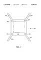
- FIG. 1shows a metal panel 100 patterned for providing six heat sink structures 101-106 of the present invention.
- FIG. 2is a top view of a heat sink 200 in accordance with the present invention.
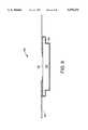
- FIG. 3is a side view of the heat sink 200 of FIG. 2.
- FIG. 4is a top view of another heat sink 250 in accordance with the present invention.
- FIG. 5is an isometric view of the heat sink 200 of FIG. 2.
- FIG. 6is a view from the bottom side of the heat sink 200 of FIG. 2, after aluminization, showing areas 301, 302a-d masked in the aluminization process so as to expose the copper block underneath, in accordance with the present invention.
- FIG. 7is a view from the top side of heat sink 200 of FIG. 6.
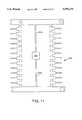
- FIG. 9shows a lead frame 500 having die attach pad 502 and tie bars 501a-s suitable for use as a lead frame 401 in the assembly 400 of FIG. 8.
- FIG. 10shows the lead frame 500 of FIG. 9 after severing die attach pad 502 at certain positions in the tie bars 501a-501d.
- the present inventionprovides a high performance high power dissipation plastic encapsulated package for an integrated circuit device.
- the plastic encapsulated packagecomprises, among other elements, a heat sink on which a lead frame and an integrated circuit die are attached.
- One embodiment of the heat sink in accordance with the present inventionis formed from a metal panel, such as metal panel 100 of FIG. 1.
- a metal panelsuch as metal panel 100 of FIG. 1.
- an array of structures, such as structures 101-106, each patterned to form a heat sinkare provided on metal panel 100.
- Metal panel 100is 0.07" thick, although any suitable thickness can also be used.
- metal panel 100can be of any suitable vertical and horizontal dimensions.
- Suitable materials for providing metal panel 100include copper and copper alloys. Such alloys include but are not limited to copper, copper and zinc, or copper and iron. If the aluminizing process described below is to be used, such copper alloys, however, should not contain sulphur, chlorine or phosphorus.
- heat sink of the present inventionis formed by an electrically conductive material this heat sink can be connected to the power or ground terminals of the integrated circuit die.
- Thermally conductive materialsuch as beryllium and certain ceramics, can also be used as heat sink. Such material typically have a lower thermal conductivity than copper, and therefore are less efficient heat dissipators.
- Structures 101-106are provided on the metal panel 100 by a photolithographical step on the surface of the metal panel 100 using a photoresist, such as du Pont's dry photo resist film applied on by lamination.
- the metal panelis then subject to a chemical etch process.
- Two examples of suitable etchants for this chemical etch processare ferrous chloride and cupric chloride.
- the etch processleaves area 108 of structure 101 intact, "half-etches" area 111 of structure 101, and completely etches areas 107a, 107b, 107c and 107d of the structure 101. In this etch process, while an area to be completely etched is etched from both top and bottom surfaces of the metal panel, a "half-etch" area is etched only from one side of the metal panel.
- the half-etched area 111 of structure 101has a thickness less than the 0.07" at the intact area 108, forming a stepped structure (see FIG. 3, described below).
- the thickness at area 108is selected to be substantially one half the height of the plastic mold used at a later step to encapsulate the heat sink, the integrated circuit die and the lead frame.
- a packagecan be made (to be described below in conjunction with FIG. 12) such that one surface of the heat sink is flush with one outer surface of the plastic encapsulation so as to facilitate heat dissipation to the external environment.
- a thinner heat sinkcan be totally encapsulated by the plastic package material.
- the structure 101can be severed from the metal panel 100 at the connecting strips 109a, 109b, 109c and 109d.
- One such severed structureis shown as the heat sink 200 or 250 in FIGS. 2-5.
- the structuresneed not be severed into individual heat sinks after the chemical etch process.
- the panelmay, however, be cut into strips each containing one row of etched heat sink structures.
- FIG. 2is a top view of a heat sink 200 in accordance with the present invention.
- heat sink 200is formed using a chemical etching step, such heat sink can also be obtained by stamping, milling or any suitable method to provide the shape shown in FIG. 2.
- FIGS. 3 and 5are respectively the side and isometric views of the heat sink 200.
- FIG. 4is the top view of another heat sink 250, which is an alternative configuration suitable for a plastic dual-in-line package (PDIP) or a smaller outline integrated circuit (SOIC) package.
- Heat sink 250has a generally more elongated shape than heat sink 200 of FIG. 2.
- the layer of nickelis provided by an electrochemical plating process known in the art to a thickness sufficient to provide a layer of barrier material, such that the deposited aluminum will not peel or blister from the surface of the heat sink during the subsequent anodization step. Without this barrier material the deposited aluminum may peel away from the copper surface.
- a vacuum deposition equipment suitable for providing the vacuum deposition stepis disclosed in U.K. Patent Application, No. 8918728.0, entitled “Aluminum vacuum deposition machine for coating parts of lead frames for IC chips, " publication no. GB 2234988, published on Feb. 20, 1991, which is hereby incorporated by reference in its entirety. Any other suitable method for providing a thin layer of aluminum can also be used.
- certain arease.g., the die attach area and the areas at which the lead frame is expected to attach
- This masking stepcan be accomplished using a metal mask placed in contact with the heat sink.
- the aluminized heat sink 200is then subjected to a "hard anodization" process known in the art, in which the deposited aluminum is oxidized to result in an electrically insulative surface, except at certain areas masked, such as those shown above in conjunction with FIGS. 6-7.
- a masking step prior to the aluminizationthe person of ordinary skill in the art will appreciate that areas exposing the nickel plated copper core can be obtained by first aluminizing the entire heat sink and then using sandblasting or other appropriate subtractive technique to remove the aluminum from the designated areas before anodizing.
- the subtractive techniqueis preferably applied before anodizing, because the anodizing process hardens the deposited aluminum, thereby making it difficult to remove.
- gold, silver or other suitable metalscan be plated onto the exposed areas, such as areas 301 and 302a-d, to enhance attachments of the integrated circuit die and the lead frame.
- the next steps after attachment of the lead frameare die attach, wire bonding and plastic encapsulation.
- the final assembly 600is shown in FIG. 12.
- the integrated circuit die, shown in FIG. 12 as integrated circuit die 601can be attached to surface 301 of the heat sink 200 using a resinous die attach, an eutectic die attach, soft solder die attach, or any other suitable die attach method known in the art.
- Wire bondingthen connects the terminal pads provided on the integrated circuit 601 to corresponding conductors on the lead frame 401.
- This bondingcan be accomplished by a thermosonic wire bonding technique using lead wires, e.g. the lead wires 602a and 602b shown in FIG. 12.
- the anodized aluminum layer 402is a relatively good thermal conductor, the anodized surface can be used to maintain via the heat sink the wire bonding temperature within the typical desirable range of 5% at the bonding surface.
- connection between the integrated circuit die 601 and the lead frame 401also can be accomplished by a tape automatic bonding (TAB) method.
- TABtape automatic bonding
- the final assembly including semiconductor die 601, bond wires, such as bond wires 602a and 602b, the heat sink 200 and the lead frame 401, except for the external lead portions,are encapsulated in a plastic material 603 customarily used to create plastic packages.
- this surface 202is flush with the plastic encapsulation 603, so that heat can be dissipated by heat sink 200 directly to the exterior. It will be appreciated that, because of the stepped structure of heat sink 200, moisture from the exterior travels a relatively long path to reach the encapsulated elements, such as bond wires 601a and 601b, resulting in enhanced moisture resistance.
- an aluminum heat sinkcan also be fabricated from an aluminum metal panel similar to the metal panel 100 described above.
- Such an aluminum heat sinkcan be anodized directly without the plating and vapor deposition steps described for the copper heat sink above.
- such an aluminum heat sinkhas a lesser thermal performance than a copper heat sink.
- the cost of providing such aluminum heat sinkis less than its copper counterpart. In some applications, where the thermal dissipation requirements are less demanding, the aluminum heat sink is a cost-effective alternative.
Landscapes
- Physics & Mathematics (AREA)
- Condensed Matter Physics & Semiconductors (AREA)
- General Physics & Mathematics (AREA)
- Engineering & Computer Science (AREA)
- Computer Hardware Design (AREA)
- Microelectronics & Electronic Packaging (AREA)
- Power Engineering (AREA)
- Cooling Or The Like Of Semiconductors Or Solid State Devices (AREA)
- Lead Frames For Integrated Circuits (AREA)
Abstract
Description
Claims (18)
Priority Applications (1)
| Application Number | Priority Date | Filing Date | Title |
|---|---|---|---|
| US08/348,288US5596231A (en) | 1991-08-05 | 1994-11-30 | High power dissipation plastic encapsulated package for integrated circuit die |
Applications Claiming Priority (3)
| Application Number | Priority Date | Filing Date | Title |
|---|---|---|---|
| US74055591A | 1991-08-05 | 1991-08-05 | |
| US98192794A | 1994-11-24 | 1994-11-24 | |
| US08/348,288US5596231A (en) | 1991-08-05 | 1994-11-30 | High power dissipation plastic encapsulated package for integrated circuit die |
Related Parent Applications (1)
| Application Number | Title | Priority Date | Filing Date |
|---|---|---|---|
| US98192794AContinuation | 1991-08-05 | 1994-11-24 |
Publications (1)
| Publication Number | Publication Date |
|---|---|
| US5596231Atrue US5596231A (en) | 1997-01-21 |
Family
ID=27113700
Family Applications (1)
| Application Number | Title | Priority Date | Filing Date |
|---|---|---|---|
| US08/348,288Expired - LifetimeUS5596231A (en) | 1991-08-05 | 1994-11-30 | High power dissipation plastic encapsulated package for integrated circuit die |
Country Status (1)
| Country | Link |
|---|---|
| US (1) | US5596231A (en) |
Cited By (80)
| Publication number | Priority date | Publication date | Assignee | Title |
|---|---|---|---|---|
| US5796160A (en)* | 1996-04-11 | 1998-08-18 | Kabushiki Kaisha Toshiba | Resin-sealed semiconductor device |
| FR2764114A1 (en)* | 1997-06-02 | 1998-12-04 | Sgs Thomson Microelectronics | SEMICONDUCTOR DEVICE PROVIDED WITH A THERMAL DISSIPATOR |
| US5854511A (en)* | 1995-11-17 | 1998-12-29 | Anam Semiconductor, Inc. | Semiconductor package including heat sink with layered conductive plate and non-conductive tape bonding to leads |
| US5886400A (en)* | 1995-08-31 | 1999-03-23 | Motorola, Inc. | Semiconductor device having an insulating layer and method for making |
| US6093960A (en)* | 1999-06-11 | 2000-07-25 | Advanced Semiconductor Engineering, Inc. | Semiconductor package having a heat spreader capable of preventing being soldered and enhancing adhesion and electrical performance |
| US6117797A (en)* | 1998-09-03 | 2000-09-12 | Micron Technology, Inc. | Attachment method for heat sinks and devices involving removal of misplaced encapsulant |
| US6159764A (en)* | 1997-07-02 | 2000-12-12 | Micron Technology, Inc. | Varied-thickness heat sink for integrated circuit (IC) packages and method of fabricating IC packages |
| US6163956A (en)* | 1998-02-23 | 2000-12-26 | Micron Technology, Inc. | Method of making chip scale package with heat spreade |
| US6242281B1 (en)* | 1998-06-10 | 2001-06-05 | Asat, Limited | Saw-singulated leadless plastic chip carrier |
| US6249050B1 (en)* | 1997-02-25 | 2001-06-19 | Micron Technology, Inc. | Encapsulated transfer molding of a semiconductor die with attached heat sink |
| US6297550B1 (en)* | 1998-04-01 | 2001-10-02 | Lsi Logic Corporation | Bondable anodized aluminum heatspreader for semiconductor packages |
| US6326687B1 (en) | 1998-09-01 | 2001-12-04 | Micron Technology, Inc. | IC package with dual heat spreaders |
| US6340842B1 (en)* | 1998-04-02 | 2002-01-22 | Oki Electric Industry Co., Ltd. | Semiconductor device in a recess of a semiconductor plate |
| US6372539B1 (en) | 2000-03-20 | 2002-04-16 | National Semiconductor Corporation | Leadless packaging process using a conductive substrate |
| US6399415B1 (en) | 2000-03-20 | 2002-06-04 | National Semiconductor Corporation | Electrical isolation in panels of leadless IC packages |
| US6404065B1 (en) | 1998-07-31 | 2002-06-11 | I-Xys Corporation | Electrically isolated power semiconductor package |
| US6444501B1 (en) | 2001-06-12 | 2002-09-03 | Micron Technology, Inc. | Two stage transfer molding method to encapsulate MMC module |
| US6452255B1 (en) | 2000-03-20 | 2002-09-17 | National Semiconductor, Corp. | Low inductance leadless package |
| US20020175399A1 (en)* | 2000-08-24 | 2002-11-28 | James Stephen L. | Packaged microelectronic devices with pressure release elements and methods for manufacturing and using such packaged microelectronic devices |
| USD466873S1 (en) | 2001-10-31 | 2002-12-10 | Siliconix Incorporated | Semiconductor chip package |
| US20020186549A1 (en)* | 2001-06-11 | 2002-12-12 | Bolken Todd O. | Alternative method used to package multi media card by transfer molding |
| US20030029633A1 (en)* | 2000-08-23 | 2003-02-13 | Ahmad Syed Sajid | Interconnecting substrates for electrical coupling of microelectronic components |
| USD472528S1 (en) | 2001-10-31 | 2003-04-01 | Siliconix Incorporated | Semiconductor chip package |
| US20030080402A1 (en)* | 1998-02-23 | 2003-05-01 | Corisis David J. | Chip scale package with heat spreader and method of manufacture |
| US20030168720A1 (en)* | 2002-03-06 | 2003-09-11 | Nichia Corporation | Semiconductor device and manufacturing method for same |
| US6621159B1 (en)* | 1999-03-19 | 2003-09-16 | Fuji Photo Film Co., Ltd. | Semiconductor light emitting device and method for manufacturing the same |
| US20030178719A1 (en)* | 2002-03-22 | 2003-09-25 | Combs Edward G. | Enhanced thermal dissipation integrated circuit package and method of manufacturing enhanced thermal dissipation integrated circuit package |
| US6657866B2 (en)* | 2002-03-15 | 2003-12-02 | Robert C. Morelock | Electronics assembly with improved heatsink configuration |
| US20030227067A1 (en)* | 2002-06-07 | 2003-12-11 | Heraeus Sensor-Nite Gmbh | Semiconductor component with integrated circuit, cooling body, and temperature sensor |
| US6664139B2 (en) | 2000-06-16 | 2003-12-16 | Micron Technology, Inc. | Method and apparatus for packaging a microelectronic die |
| US20030234454A1 (en)* | 2002-06-24 | 2003-12-25 | Serafin Pedron | Integrated circuit package and method of manufacturing the integrated circuit package |
| US6686652B1 (en)* | 2000-03-20 | 2004-02-03 | National Semiconductor | Locking lead tips and die attach pad for a leadless package apparatus and method |
| US6705388B1 (en) | 1997-11-10 | 2004-03-16 | Parker-Hannifin Corporation | Non-electrically conductive thermal dissipator for electronic components |
| US6727585B2 (en) | 2001-05-04 | 2004-04-27 | Ixys Corporation | Power device with a plastic molded package and direct bonded substrate |
| US6731002B2 (en) | 2001-05-04 | 2004-05-04 | Ixys Corporation | High frequency power device with a plastic molded package and direct bonded substrate |
| US20040084431A1 (en)* | 2002-09-02 | 2004-05-06 | Catem Gmbh & Co. Kg; | Electric heating for motor vehicles |
| US6734552B2 (en) | 2001-07-11 | 2004-05-11 | Asat Limited | Enhanced thermal dissipation integrated circuit package |
| US6790710B2 (en)* | 2002-01-31 | 2004-09-14 | Asat Limited | Method of manufacturing an integrated circuit package |
| US6838760B1 (en) | 2000-08-28 | 2005-01-04 | Micron Technology, Inc. | Packaged microelectronic devices with interconnecting units |
| US7015072B2 (en) | 2001-07-11 | 2006-03-21 | Asat Limited | Method of manufacturing an enhanced thermal dissipation integrated circuit package |
| US7038305B1 (en) | 2003-07-15 | 2006-05-02 | Altera Corp. | Package for integrated circuit die |
| US20060261498A1 (en)* | 2005-05-17 | 2006-11-23 | Micron Technology, Inc. | Methods and apparatuses for encapsulating microelectronic devices |
| US20060273451A1 (en)* | 2005-06-01 | 2006-12-07 | Tdk Corporation | Semiconductor IC and its manufacturing method, and module with embedded semiconductor IC and its manufacturing method |
| CN100374313C (en)* | 2004-03-02 | 2008-03-12 | 凯特姆两合公司 | Electric heating device for motor vehicle |
| US20080206930A1 (en)* | 2007-02-23 | 2008-08-28 | Micron Technology, Inc. | Systems and methods for compressing an encapsulant adjacent a semiconductor workpiece |
| US20090209064A1 (en)* | 2006-04-28 | 2009-08-20 | Somchai Nonahasitthichai | Lead frame land grid array |
| US7790512B1 (en) | 2007-11-06 | 2010-09-07 | Utac Thai Limited | Molded leadframe substrate semiconductor package |
| US20100230802A1 (en)* | 2009-03-12 | 2010-09-16 | Utac Thai Limited | Metallic solderability preservation coating on metal part of semiconductor package to prevent oxide |
| US7827679B1 (en)* | 2006-04-20 | 2010-11-09 | Rati M. Patel | Thermal management circuit board and methods of producing the same |
| US20100311208A1 (en)* | 2008-05-22 | 2010-12-09 | Utac Thai Limited | Method and apparatus for no lead semiconductor package |
| US20100327432A1 (en)* | 2006-09-26 | 2010-12-30 | Utac Thai Limited | Package with heat transfer |
| US20110018111A1 (en)* | 2009-07-23 | 2011-01-27 | Utac Thai Limited | Leadframe feature to minimize flip-chip semiconductor die collapse during flip-chip reflow |
| US20110039371A1 (en)* | 2008-09-04 | 2011-02-17 | Utac Thai Limited | Flip chip cavity package |
| US20110133319A1 (en)* | 2009-12-04 | 2011-06-09 | Utac Thai Limited | Auxiliary leadframe member for stabilizing the bond wire process |
| US20110147931A1 (en)* | 2006-04-28 | 2011-06-23 | Utac Thai Limited | Lead frame land grid array with routing connector trace under unit |
| US20110198752A1 (en)* | 2006-04-28 | 2011-08-18 | Utac Thai Limited | Lead frame ball grid array with traces under die |
| US8013437B1 (en) | 2006-09-26 | 2011-09-06 | Utac Thai Limited | Package with heat transfer |
| US20110221051A1 (en)* | 2010-03-11 | 2011-09-15 | Utac Thai Limited | Leadframe based multi terminal ic package |
| US20120037930A1 (en)* | 2009-04-03 | 2012-02-16 | Osram Opto Semiconductors Gmbh | Method for producing an optoelectronic component, optoelectronic component, and component arrangement having a plurality of optoelectronic components |
| US20120235292A1 (en)* | 2011-03-18 | 2012-09-20 | Shinko Electric Industries Co., Ltd. | Heat radiating component and semiconductor package having the same |
| US8330270B1 (en) | 1998-06-10 | 2012-12-11 | Utac Hong Kong Limited | Integrated circuit package having a plurality of spaced apart pad portions |
| US8461694B1 (en) | 2006-04-28 | 2013-06-11 | Utac Thai Limited | Lead frame ball grid array with traces under die having interlocking features |
| US8460970B1 (en) | 2006-04-28 | 2013-06-11 | Utac Thai Limited | Lead frame ball grid array with traces under die having interlocking features |
| US20130200509A1 (en)* | 2012-02-02 | 2013-08-08 | Samsung Electronics Co., Ltd. | Semiconductor package |
| US20140070397A1 (en)* | 2012-09-13 | 2014-03-13 | Lakshminarayan Viswanathan | High power semiconductor package subsystems |
| US20140217523A1 (en)* | 2011-07-29 | 2014-08-07 | Epcos Ag | Housing for a Semiconductor Chip and Semiconductor Chip with a Housing |
| US8871571B2 (en) | 2010-04-02 | 2014-10-28 | Utac Thai Limited | Apparatus for and methods of attaching heat slugs to package tops |
| US9000590B2 (en) | 2012-05-10 | 2015-04-07 | Utac Thai Limited | Protruding terminals with internal routing interconnections semiconductor device |
| US9006034B1 (en) | 2012-06-11 | 2015-04-14 | Utac Thai Limited | Post-mold for semiconductor package having exposed traces |
| US9082607B1 (en) | 2006-12-14 | 2015-07-14 | Utac Thai Limited | Molded leadframe substrate semiconductor package |
| US9355940B1 (en) | 2009-12-04 | 2016-05-31 | Utac Thai Limited | Auxiliary leadframe member for stabilizing the bond wire process |
| US9449905B2 (en) | 2012-05-10 | 2016-09-20 | Utac Thai Limited | Plated terminals with routing interconnections semiconductor device |
| KR101682067B1 (en) | 2015-08-26 | 2016-12-02 | 제엠제코(주) | Semiconductor package with heat slug and leadframe bonded using ultrasonic welding |
| US9761435B1 (en) | 2006-12-14 | 2017-09-12 | Utac Thai Limited | Flip chip cavity package |
| US9805955B1 (en) | 2015-11-10 | 2017-10-31 | UTAC Headquarters Pte. Ltd. | Semiconductor package with multiple molding routing layers and a method of manufacturing the same |
| US10242953B1 (en) | 2015-05-27 | 2019-03-26 | Utac Headquarters PTE. Ltd | Semiconductor package with plated metal shielding and a method thereof |
| US10242934B1 (en) | 2014-05-07 | 2019-03-26 | Utac Headquarters Pte Ltd. | Semiconductor package with full plating on contact side surfaces and methods thereof |
| US10276477B1 (en) | 2016-05-20 | 2019-04-30 | UTAC Headquarters Pte. Ltd. | Semiconductor package with multiple stacked leadframes and a method of manufacturing the same |
| US11171077B2 (en)* | 2019-07-10 | 2021-11-09 | Nxp Usa, Inc. | Semiconductor device with lead frame that accommodates various die sizes |
| US20220028798A1 (en)* | 2020-07-21 | 2022-01-27 | UTAC Headquarters Pte. Ltd. | Semiconductor packages with integrated shielding |
Citations (12)
| Publication number | Priority date | Publication date | Assignee | Title |
|---|---|---|---|---|
| US3469017A (en)* | 1967-12-12 | 1969-09-23 | Rca Corp | Encapsulated semiconductor device having internal shielding |
| US3611065A (en)* | 1968-09-30 | 1971-10-05 | Siemens Ag | Carrier for semiconductor components |
| US3646409A (en)* | 1968-07-30 | 1972-02-29 | Philips Corp | Heat-sinking package for semiconductor integrated circuit |
| JPS522281A (en)* | 1975-06-24 | 1977-01-08 | Hitachi Ltd | Method of making semiconductor devices |
| US4518983A (en)* | 1982-10-22 | 1985-05-21 | Westinghouse Electric Corp. | Assembly-heat sink for semiconductor devices |
| JPS6116605A (en)* | 1984-07-02 | 1986-01-24 | Hitachi Ltd | Variable gain amplifying circuit |
| US4796083A (en)* | 1987-07-02 | 1989-01-03 | Olin Corporation | Semiconductor casing |
| US4811166A (en)* | 1986-07-02 | 1989-03-07 | Texas Instruments Incorporated | Heat dissipating member for mounting a semiconductor device and electrical circuit unit incorporating the member |
| US4916518A (en)* | 1983-01-25 | 1990-04-10 | Tokyo Shibaura Denki Kabushiki Kaisha | Plastic encapsulated semiconductor device and method for manufacturing the same |
| US4961106A (en)* | 1987-03-27 | 1990-10-02 | Olin Corporation | Metal packages having improved thermal dissipation |
| US4971633A (en)* | 1989-09-26 | 1990-11-20 | The United States Of America As Represented By The Department Of Energy | Photovoltaic cell assembly |
| US4975761A (en)* | 1989-09-05 | 1990-12-04 | Advanced Micro Devices, Inc. | High performance plastic encapsulated package for integrated circuit die |
- 1994
- 1994-11-30USUS08/348,288patent/US5596231A/ennot_activeExpired - Lifetime
Patent Citations (12)
| Publication number | Priority date | Publication date | Assignee | Title |
|---|---|---|---|---|
| US3469017A (en)* | 1967-12-12 | 1969-09-23 | Rca Corp | Encapsulated semiconductor device having internal shielding |
| US3646409A (en)* | 1968-07-30 | 1972-02-29 | Philips Corp | Heat-sinking package for semiconductor integrated circuit |
| US3611065A (en)* | 1968-09-30 | 1971-10-05 | Siemens Ag | Carrier for semiconductor components |
| JPS522281A (en)* | 1975-06-24 | 1977-01-08 | Hitachi Ltd | Method of making semiconductor devices |
| US4518983A (en)* | 1982-10-22 | 1985-05-21 | Westinghouse Electric Corp. | Assembly-heat sink for semiconductor devices |
| US4916518A (en)* | 1983-01-25 | 1990-04-10 | Tokyo Shibaura Denki Kabushiki Kaisha | Plastic encapsulated semiconductor device and method for manufacturing the same |
| JPS6116605A (en)* | 1984-07-02 | 1986-01-24 | Hitachi Ltd | Variable gain amplifying circuit |
| US4811166A (en)* | 1986-07-02 | 1989-03-07 | Texas Instruments Incorporated | Heat dissipating member for mounting a semiconductor device and electrical circuit unit incorporating the member |
| US4961106A (en)* | 1987-03-27 | 1990-10-02 | Olin Corporation | Metal packages having improved thermal dissipation |
| US4796083A (en)* | 1987-07-02 | 1989-01-03 | Olin Corporation | Semiconductor casing |
| US4975761A (en)* | 1989-09-05 | 1990-12-04 | Advanced Micro Devices, Inc. | High performance plastic encapsulated package for integrated circuit die |
| US4971633A (en)* | 1989-09-26 | 1990-11-20 | The United States Of America As Represented By The Department Of Energy | Photovoltaic cell assembly |
Non-Patent Citations (2)
| Title |
|---|
| Electrical isolation of copper thermal cooling device by anodizing aluminum layer on cavity walls.* |
| IBM Technical Disclosure Bulletin vol. 33, No. 3A Aug. 1990.* |
Cited By (203)
| Publication number | Priority date | Publication date | Assignee | Title |
|---|---|---|---|---|
| US5886400A (en)* | 1995-08-31 | 1999-03-23 | Motorola, Inc. | Semiconductor device having an insulating layer and method for making |
| US5854511A (en)* | 1995-11-17 | 1998-12-29 | Anam Semiconductor, Inc. | Semiconductor package including heat sink with layered conductive plate and non-conductive tape bonding to leads |
| US5796160A (en)* | 1996-04-11 | 1998-08-18 | Kabushiki Kaisha Toshiba | Resin-sealed semiconductor device |
| US6583504B2 (en) | 1997-02-25 | 2003-06-24 | Micron Technology, Inc. | Semiconductor die with attached heat sink and transfer mold |
| US20020076856A1 (en)* | 1997-02-25 | 2002-06-20 | Wensel Richard W. | Method and apparatus for transfer molding encapsulation of a semiconductor die with attached heat sink |
| US6869811B2 (en) | 1997-02-25 | 2005-03-22 | Micron Technology, Inc. | Methods for transfer molding encapsulation of a semiconductor die with attached heat sink |
| US6403387B1 (en) | 1997-02-25 | 2002-06-11 | Micron Technology | Method and apparatus for transfer molding encapsulation of a semiconductor die with attached heat sink |
| US20040004274A1 (en)* | 1997-02-25 | 2004-01-08 | Wensel Richard W. | Semiconductor die with attached heat sink and transfer mold |
| US6373132B2 (en) | 1997-02-25 | 2002-04-16 | Micron Technology, Inc. | Semiconductor die with attached heat sink and transfer mold |
| US20040033644A1 (en)* | 1997-02-25 | 2004-02-19 | Wensel Richard W. | Methods for transfer molding encapsulation of a semiconductor die with attached heat sink |
| US7061082B2 (en) | 1997-02-25 | 2006-06-13 | Micron Technology, Inc. | Semiconductor die with attached heat sink and transfer mold |
| US6249050B1 (en)* | 1997-02-25 | 2001-06-19 | Micron Technology, Inc. | Encapsulated transfer molding of a semiconductor die with attached heat sink |
| EP0883177A1 (en)* | 1997-06-02 | 1998-12-09 | STMicroelectronics S.A. | Semiconductor device with heat sink |
| US6064115A (en)* | 1997-06-02 | 2000-05-16 | Sgs-Thomson Microelectronics S.A. | Semiconductor device provided with a heat sink |
| FR2764114A1 (en)* | 1997-06-02 | 1998-12-04 | Sgs Thomson Microelectronics | SEMICONDUCTOR DEVICE PROVIDED WITH A THERMAL DISSIPATOR |
| US6506629B1 (en) | 1997-07-02 | 2003-01-14 | Micron Technology, Inc. | Varied-thickness heat sink for integrated circuit (IC) packages and method of fabricating IC packages |
| US20030077853A1 (en)* | 1997-07-02 | 2003-04-24 | Kinsman Larry D. | Varied-thickness heat sink for integrated circuit (IC) packages and method of fabricating IC packages |
| US6159764A (en)* | 1997-07-02 | 2000-12-12 | Micron Technology, Inc. | Varied-thickness heat sink for integrated circuit (IC) packages and method of fabricating IC packages |
| US7125749B2 (en) | 1997-07-02 | 2006-10-24 | Micron Technology, Inc. | Varied-thickness heat sink for integrated circuit (IC) packages and method of fabricating IC packages |
| US20060267184A1 (en)* | 1997-07-02 | 2006-11-30 | Kinsman Larry D | Varied-thickness heat sink for integrated circuit (IC) package |
| US6705388B1 (en) | 1997-11-10 | 2004-03-16 | Parker-Hannifin Corporation | Non-electrically conductive thermal dissipator for electronic components |
| US7312516B2 (en) | 1998-02-23 | 2007-12-25 | Micron Technology, Inc. | Chip scale package with heat spreader |
| US20050248038A1 (en)* | 1998-02-23 | 2005-11-10 | Corisis David J | Chip scale package with heat spreader |
| US6735859B2 (en) | 1998-02-23 | 2004-05-18 | Micron Technology, Inc. | Method of manufacturing chip scale package |
| US20030080402A1 (en)* | 1998-02-23 | 2003-05-01 | Corisis David J. | Chip scale package with heat spreader and method of manufacture |
| US20060186533A1 (en)* | 1998-02-23 | 2006-08-24 | Corisis David J | Chip scale package with heat spreader |
| US7233056B1 (en) | 1998-02-23 | 2007-06-19 | Micron Technology, Inc. | Chip scale package with heat spreader |
| US6314639B1 (en) | 1998-02-23 | 2001-11-13 | Micron Technology, Inc. | Chip scale package with heat spreader and method of manufacture |
| US6505400B1 (en) | 1998-02-23 | 2003-01-14 | Micron Technology, Inc. | Method of making chip scale package with heat spreader |
| US6163956A (en)* | 1998-02-23 | 2000-12-26 | Micron Technology, Inc. | Method of making chip scale package with heat spreade |
| US6297550B1 (en)* | 1998-04-01 | 2001-10-02 | Lsi Logic Corporation | Bondable anodized aluminum heatspreader for semiconductor packages |
| US6340842B1 (en)* | 1998-04-02 | 2002-01-22 | Oki Electric Industry Co., Ltd. | Semiconductor device in a recess of a semiconductor plate |
| US6538322B2 (en)* | 1998-04-02 | 2003-03-25 | Oki Electric Industry Co., Ltd. | Semiconductor device in a recess of a semiconductor plate |
| US20030122223A1 (en)* | 1998-04-02 | 2003-07-03 | Akio Nakamura | Semiconductor device in a recess of a semiconductor plate |
| US7183132B2 (en) | 1998-04-02 | 2007-02-27 | Oki Electric Industry Co., Ltd. | Semiconductor device in a recess of a semiconductor plate |
| US8330270B1 (en) | 1998-06-10 | 2012-12-11 | Utac Hong Kong Limited | Integrated circuit package having a plurality of spaced apart pad portions |
| US7482690B1 (en) | 1998-06-10 | 2009-01-27 | Asat Ltd. | Electronic components such as thin array plastic packages and process for fabricating same |
| US6242281B1 (en)* | 1998-06-10 | 2001-06-05 | Asat, Limited | Saw-singulated leadless plastic chip carrier |
| US6710463B2 (en) | 1998-07-31 | 2004-03-23 | Ixys Corporation | Electrically isolated power semiconductor package |
| US6534343B2 (en) | 1998-07-31 | 2003-03-18 | Ixys Corporation | Method of making electrically isolated power semiconductor package |
| US6404065B1 (en) | 1998-07-31 | 2002-06-11 | I-Xys Corporation | Electrically isolated power semiconductor package |
| US6920688B2 (en) | 1998-09-01 | 2005-07-26 | Micron Technology, Inc. | Method for a semiconductor assembly having a semiconductor die with dual heat spreaders |
| US6326687B1 (en) | 1998-09-01 | 2001-12-04 | Micron Technology, Inc. | IC package with dual heat spreaders |
| US20020185727A1 (en)* | 1998-09-01 | 2002-12-12 | Corisis David J. | IC package with dual heat spreaders |
| US6765291B2 (en) | 1998-09-01 | 2004-07-20 | Micron Technology, Inc. | IC package with dual heat spreaders |
| US6518098B2 (en) | 1998-09-01 | 2003-02-11 | Micron Technology, Inc. | IC package with dual heat spreaders |
| US6596565B1 (en) | 1998-09-03 | 2003-07-22 | Micron Technology, Inc. | Chip on board and heat sink attachment methods |
| US6784113B2 (en) | 1998-09-03 | 2004-08-31 | Micron Technology, Inc. | Chip on board and heat sink attachment methods |
| US6806567B2 (en) | 1998-09-03 | 2004-10-19 | Micron Technology, Inc. | Chip on board with heat sink attachment and assembly |
| US20040126931A1 (en)* | 1998-09-03 | 2004-07-01 | Hembree David R. | Chip on board and heat sink attachment methods |
| US6630371B2 (en) | 1998-09-03 | 2003-10-07 | Micron Technology, Inc. | Chip on board and heat sink attachment methods |
| US6432840B1 (en) | 1998-09-03 | 2002-08-13 | Micron Technology, Inc. | Methodology of removing misplaced encapsulant for attachment of heat sinks in a chip on board package |
| US6451709B1 (en) | 1998-09-03 | 2002-09-17 | Micron Technology, Inc. | Methodology of removing misplaced encapsulant for attachment of heat sinks in a chip on board package |
| US7244637B2 (en) | 1998-09-03 | 2007-07-17 | Micron Technology, Inc. | Chip on board and heat sink attachment methods |
| US6229204B1 (en) | 1998-09-03 | 2001-05-08 | Micron Technology, Inc. | Chip on board with heat sink attachment |
| US6117797A (en)* | 1998-09-03 | 2000-09-12 | Micron Technology, Inc. | Attachment method for heat sinks and devices involving removal of misplaced encapsulant |
| US6621159B1 (en)* | 1999-03-19 | 2003-09-16 | Fuji Photo Film Co., Ltd. | Semiconductor light emitting device and method for manufacturing the same |
| US6093960A (en)* | 1999-06-11 | 2000-07-25 | Advanced Semiconductor Engineering, Inc. | Semiconductor package having a heat spreader capable of preventing being soldered and enhancing adhesion and electrical performance |
| US6372539B1 (en) | 2000-03-20 | 2002-04-16 | National Semiconductor Corporation | Leadless packaging process using a conductive substrate |
| US6452255B1 (en) | 2000-03-20 | 2002-09-17 | National Semiconductor, Corp. | Low inductance leadless package |
| US6399415B1 (en) | 2000-03-20 | 2002-06-04 | National Semiconductor Corporation | Electrical isolation in panels of leadless IC packages |
| US6686652B1 (en)* | 2000-03-20 | 2004-02-03 | National Semiconductor | Locking lead tips and die attach pad for a leadless package apparatus and method |
| US6683388B2 (en) | 2000-06-16 | 2004-01-27 | Micron Technology, Inc. | Method and apparatus for packaging a microelectronic die |
| US6677675B2 (en)* | 2000-06-16 | 2004-01-13 | Micron Technology, Inc. | Microelectronic devices and microelectronic die packages |
| US6664139B2 (en) | 2000-06-16 | 2003-12-16 | Micron Technology, Inc. | Method and apparatus for packaging a microelectronic die |
| US6796028B2 (en) | 2000-08-23 | 2004-09-28 | Micron Technology, Inc. | Method of Interconnecting substrates for electrical coupling of microelectronic components |
| US6983551B2 (en) | 2000-08-23 | 2006-01-10 | Micron Technology, Inc. | Interconnecting substrates for electrical coupling of microelectronic components |
| US6982386B2 (en) | 2000-08-23 | 2006-01-03 | Micron Technology, Inc. | Interconnecting substrates for electrical coupling of microelectronic components |
| US20030109083A1 (en)* | 2000-08-23 | 2003-06-12 | Ahmad Syed Sajid | Interconnecting substrates for electrical coupling of microelectronic components |
| US20030106709A1 (en)* | 2000-08-23 | 2003-06-12 | Ahmad Syed Sajid | Interconnecting substrates for electrical coupling of microelectronic components |
| US20030029633A1 (en)* | 2000-08-23 | 2003-02-13 | Ahmad Syed Sajid | Interconnecting substrates for electrical coupling of microelectronic components |
| US20060180907A1 (en)* | 2000-08-24 | 2006-08-17 | Micron Technology, Inc. | Packaged microelectronic devices with pressure release elements and methods for manufacturing and using such packaged microelectonic devices |
| US20020175399A1 (en)* | 2000-08-24 | 2002-11-28 | James Stephen L. | Packaged microelectronic devices with pressure release elements and methods for manufacturing and using such packaged microelectronic devices |
| US6979595B1 (en) | 2000-08-24 | 2005-12-27 | Micron Technology, Inc. | Packaged microelectronic devices with pressure release elements and methods for manufacturing and using such packaged microelectronic devices |
| US7049685B2 (en) | 2000-08-24 | 2006-05-23 | Micron Technology, Inc. | Packaged microelectronic devices with pressure release elements and methods for manufacturing and using such packaged microelectronic devices |
| US7101737B2 (en) | 2000-08-28 | 2006-09-05 | Micron Technology, Inc. | Method of encapsulating interconnecting units in packaged microelectronic devices |
| US7332376B2 (en) | 2000-08-28 | 2008-02-19 | Micron Technology, Inc. | Method of encapsulating packaged microelectronic devices with a barrier |
| US20070063335A1 (en)* | 2000-08-28 | 2007-03-22 | Micron Technology, Inc. | Packaged microelectronic devices with interconnecting units and methods for manufacturing and using the interconnecting units |
| US6838760B1 (en) | 2000-08-28 | 2005-01-04 | Micron Technology, Inc. | Packaged microelectronic devices with interconnecting units |
| US6727585B2 (en) | 2001-05-04 | 2004-04-27 | Ixys Corporation | Power device with a plastic molded package and direct bonded substrate |
| US6731002B2 (en) | 2001-05-04 | 2004-05-04 | Ixys Corporation | High frequency power device with a plastic molded package and direct bonded substrate |
| US20050023583A1 (en)* | 2001-06-11 | 2005-02-03 | Bolken Todd O. | Multi media card formed by transfer molding |
| US20050022378A1 (en)* | 2001-06-11 | 2005-02-03 | Bolken Todd O. | Apparatus used to package multimedia card by transfer molding |
| US20060157838A1 (en)* | 2001-06-11 | 2006-07-20 | Bolken Todd O | Multimedia card and transfer molding method |
| US20020186549A1 (en)* | 2001-06-11 | 2002-12-12 | Bolken Todd O. | Alternative method used to package multi media card by transfer molding |
| US7220615B2 (en) | 2001-06-11 | 2007-05-22 | Micron Technology, Inc. | Alternative method used to package multimedia card by transfer molding |
| US7288441B2 (en) | 2001-06-12 | 2007-10-30 | Micron Technology, Inc. | Method for two-stage transfer molding device to encapsulate MMC module |
| US7279781B2 (en) | 2001-06-12 | 2007-10-09 | Micron Technology, Inc. | Two-stage transfer molding device to encapsulate MMC module |
| US20020190429A1 (en)* | 2001-06-12 | 2002-12-19 | Bolken Todd O. | Two-stage transfer molding method to encapsulate MMC module |
| US6764882B2 (en) | 2001-06-12 | 2004-07-20 | Micron Technology, Inc. | Two-stage transfer molding method to encapsulate MMC module |
| US6730995B2 (en) | 2001-06-12 | 2004-05-04 | Micron Technology, Inc. | Two-stage transfer molding device to encapsulate MMC module |
| US20040169265A1 (en)* | 2001-06-12 | 2004-09-02 | Bolken Todd O. | Two-stage transfer molding device to encapsulate MMC module |
| US6538311B2 (en) | 2001-06-12 | 2003-03-25 | Micron Technology, Inc. | Two-stage transfer molding method to encapsulate MMC module |
| US20060110850A1 (en)* | 2001-06-12 | 2006-05-25 | Bolken Todd O | Method for two-stage transfer molding device to encapsulate MMC module |
| US6444501B1 (en) | 2001-06-12 | 2002-09-03 | Micron Technology, Inc. | Two stage transfer molding method to encapsulate MMC module |
| US20030137060A1 (en)* | 2001-06-12 | 2003-07-24 | Bolken Todd O. | Two-stage transfer molding method to encapsulate MMC module |
| US7015072B2 (en) | 2001-07-11 | 2006-03-21 | Asat Limited | Method of manufacturing an enhanced thermal dissipation integrated circuit package |
| US6734552B2 (en) | 2001-07-11 | 2004-05-11 | Asat Limited | Enhanced thermal dissipation integrated circuit package |
| US20060223237A1 (en)* | 2001-07-11 | 2006-10-05 | Combs Edward G | Method of manufacturing enhanced thermal dissipation integrated circuit package |
| USD472528S1 (en) | 2001-10-31 | 2003-04-01 | Siliconix Incorporated | Semiconductor chip package |
| USD466873S1 (en) | 2001-10-31 | 2002-12-10 | Siliconix Incorporated | Semiconductor chip package |
| US6790710B2 (en)* | 2002-01-31 | 2004-09-14 | Asat Limited | Method of manufacturing an integrated circuit package |
| US20050077613A1 (en)* | 2002-01-31 | 2005-04-14 | Mclellan Neil Robert | Integrated circuit package |
| US20030168720A1 (en)* | 2002-03-06 | 2003-09-11 | Nichia Corporation | Semiconductor device and manufacturing method for same |
| US6943433B2 (en)* | 2002-03-06 | 2005-09-13 | Nichia Corporation | Semiconductor device and manufacturing method for same |
| US6657866B2 (en)* | 2002-03-15 | 2003-12-02 | Robert C. Morelock | Electronics assembly with improved heatsink configuration |
| US20040046241A1 (en)* | 2002-03-22 | 2004-03-11 | Combs Edward G. | Method of manufacturing enhanced thermal dissipation integrated circuit package |
| US20030178719A1 (en)* | 2002-03-22 | 2003-09-25 | Combs Edward G. | Enhanced thermal dissipation integrated circuit package and method of manufacturing enhanced thermal dissipation integrated circuit package |
| US6787870B2 (en) | 2002-06-07 | 2004-09-07 | Heraeus Sensor Technology Gmbh | Semiconductor component with integrated circuit, cooling body, and temperature sensor |
| US20030227067A1 (en)* | 2002-06-07 | 2003-12-11 | Heraeus Sensor-Nite Gmbh | Semiconductor component with integrated circuit, cooling body, and temperature sensor |
| US20030234454A1 (en)* | 2002-06-24 | 2003-12-25 | Serafin Pedron | Integrated circuit package and method of manufacturing the integrated circuit package |
| US6940154B2 (en) | 2002-06-24 | 2005-09-06 | Asat Limited | Integrated circuit package and method of manufacturing the integrated circuit package |
| US20040084431A1 (en)* | 2002-09-02 | 2004-05-06 | Catem Gmbh & Co. Kg; | Electric heating for motor vehicles |
| US6919535B2 (en)* | 2002-09-02 | 2005-07-19 | Catem Gmbh & Co. Kg | Electric heating for motor vehicles |
| US7038305B1 (en) | 2003-07-15 | 2006-05-02 | Altera Corp. | Package for integrated circuit die |
| CN100374313C (en)* | 2004-03-02 | 2008-03-12 | 凯特姆两合公司 | Electric heating device for motor vehicle |
| US20100178737A1 (en)* | 2005-01-06 | 2010-07-15 | Tdk Corporation | Semiconductor IC and Its Manufacturing Method, and Module with Embedded Semiconductor IC and Its Manufacturing Method |
| US20060261498A1 (en)* | 2005-05-17 | 2006-11-23 | Micron Technology, Inc. | Methods and apparatuses for encapsulating microelectronic devices |
| US20060273451A1 (en)* | 2005-06-01 | 2006-12-07 | Tdk Corporation | Semiconductor IC and its manufacturing method, and module with embedded semiconductor IC and its manufacturing method |
| US7827679B1 (en)* | 2006-04-20 | 2010-11-09 | Rati M. Patel | Thermal management circuit board and methods of producing the same |
| US20090209064A1 (en)* | 2006-04-28 | 2009-08-20 | Somchai Nonahasitthichai | Lead frame land grid array |
| US8487451B2 (en) | 2006-04-28 | 2013-07-16 | Utac Thai Limited | Lead frame land grid array with routing connector trace under unit |
| US8704381B2 (en) | 2006-04-28 | 2014-04-22 | Utac Thai Limited | Very extremely thin semiconductor package |
| US8685794B2 (en) | 2006-04-28 | 2014-04-01 | Utac Thai Limited | Lead frame land grid array with routing connector trace under unit |
| US9099317B2 (en) | 2006-04-28 | 2015-08-04 | Utac Thai Limited | Method for forming lead frame land grid array |
| US8652879B2 (en) | 2006-04-28 | 2014-02-18 | Utac Thai Limited | Lead frame ball grid array with traces under die |
| US8575762B2 (en) | 2006-04-28 | 2013-11-05 | Utac Thai Limited | Very extremely thin semiconductor package |
| US8310060B1 (en) | 2006-04-28 | 2012-11-13 | Utac Thai Limited | Lead frame land grid array |
| US8492906B2 (en) | 2006-04-28 | 2013-07-23 | Utac Thai Limited | Lead frame ball grid array with traces under die |
| US20100127363A1 (en)* | 2006-04-28 | 2010-05-27 | Utac Thai Limited | Very extremely thin semiconductor package |
| US8460970B1 (en) | 2006-04-28 | 2013-06-11 | Utac Thai Limited | Lead frame ball grid array with traces under die having interlocking features |
| US20110147931A1 (en)* | 2006-04-28 | 2011-06-23 | Utac Thai Limited | Lead frame land grid array with routing connector trace under unit |
| US20110198752A1 (en)* | 2006-04-28 | 2011-08-18 | Utac Thai Limited | Lead frame ball grid array with traces under die |
| US8461694B1 (en) | 2006-04-28 | 2013-06-11 | Utac Thai Limited | Lead frame ball grid array with traces under die having interlocking features |
| US8013437B1 (en) | 2006-09-26 | 2011-09-06 | Utac Thai Limited | Package with heat transfer |
| US8125077B2 (en) | 2006-09-26 | 2012-02-28 | Utac Thai Limited | Package with heat transfer |
| US20100327432A1 (en)* | 2006-09-26 | 2010-12-30 | Utac Thai Limited | Package with heat transfer |
| US9093486B2 (en) | 2006-12-14 | 2015-07-28 | Utac Thai Limited | Molded leadframe substrate semiconductor package |
| US9711343B1 (en) | 2006-12-14 | 2017-07-18 | Utac Thai Limited | Molded leadframe substrate semiconductor package |
| US9082607B1 (en) | 2006-12-14 | 2015-07-14 | Utac Thai Limited | Molded leadframe substrate semiconductor package |
| US9099294B1 (en) | 2006-12-14 | 2015-08-04 | Utac Thai Limited | Molded leadframe substrate semiconductor package |
| US9899208B2 (en) | 2006-12-14 | 2018-02-20 | Utac Thai Limited | Molded leadframe substrate semiconductor package |
| US9196470B1 (en) | 2006-12-14 | 2015-11-24 | Utac Thai Limited | Molded leadframe substrate semiconductor package |
| US9761435B1 (en) | 2006-12-14 | 2017-09-12 | Utac Thai Limited | Flip chip cavity package |
| US20080206930A1 (en)* | 2007-02-23 | 2008-08-28 | Micron Technology, Inc. | Systems and methods for compressing an encapsulant adjacent a semiconductor workpiece |
| US7833456B2 (en) | 2007-02-23 | 2010-11-16 | Micron Technology, Inc. | Systems and methods for compressing an encapsulant adjacent a semiconductor workpiece |
| US8338922B1 (en) | 2007-11-06 | 2012-12-25 | Utac Thai Limited | Molded leadframe substrate semiconductor package |
| US7790512B1 (en) | 2007-11-06 | 2010-09-07 | Utac Thai Limited | Molded leadframe substrate semiconductor package |
| US8063470B1 (en) | 2008-05-22 | 2011-11-22 | Utac Thai Limited | Method and apparatus for no lead semiconductor package |
| US20100311208A1 (en)* | 2008-05-22 | 2010-12-09 | Utac Thai Limited | Method and apparatus for no lead semiconductor package |
| US8071426B2 (en) | 2008-05-22 | 2011-12-06 | Utac Thai Limited | Method and apparatus for no lead semiconductor package |
| US9947605B2 (en) | 2008-09-04 | 2018-04-17 | UTAC Headquarters Pte. Ltd. | Flip chip cavity package |
| US20110039371A1 (en)* | 2008-09-04 | 2011-02-17 | Utac Thai Limited | Flip chip cavity package |
| US8569877B2 (en) | 2009-03-12 | 2013-10-29 | Utac Thai Limited | Metallic solderability preservation coating on metal part of semiconductor package to prevent oxide |
| US20110232693A1 (en)* | 2009-03-12 | 2011-09-29 | Utac Thai Limited | Metallic solderability preservation coating on metal part of semiconductor package to prevent oxide |
| US8367476B2 (en) | 2009-03-12 | 2013-02-05 | Utac Thai Limited | Metallic solderability preservation coating on metal part of semiconductor package to prevent oxide |
| US20100233854A1 (en)* | 2009-03-12 | 2010-09-16 | Utac Thai Limited | Metallic solderability preservation coating on metal part of semiconductor package to prevent oxide |
| US20100230802A1 (en)* | 2009-03-12 | 2010-09-16 | Utac Thai Limited | Metallic solderability preservation coating on metal part of semiconductor package to prevent oxide |
| US8431443B2 (en) | 2009-03-12 | 2013-04-30 | Utac Thai Limited | Metallic solderability preservation coating on metal part of semiconductor package to prevent oxide |
| US20120037930A1 (en)* | 2009-04-03 | 2012-02-16 | Osram Opto Semiconductors Gmbh | Method for producing an optoelectronic component, optoelectronic component, and component arrangement having a plurality of optoelectronic components |
| US9240523B2 (en)* | 2009-04-03 | 2016-01-19 | Osram Opto Semiconductors Gmbh | Method for producing an optoelectronic component, optoelectronic component, and component arrangement having a plurality of optoelectronic components |
| EP2415086B1 (en)* | 2009-04-03 | 2019-02-27 | OSRAM Opto Semiconductors GmbH | Method for producing an optoelectronic component, optoelectronic component, and component arrangement having a plurality of optoelectronic components |
| US20110018111A1 (en)* | 2009-07-23 | 2011-01-27 | Utac Thai Limited | Leadframe feature to minimize flip-chip semiconductor die collapse during flip-chip reflow |
| US9449900B2 (en) | 2009-07-23 | 2016-09-20 | UTAC Headquarters Pte. Ltd. | Leadframe feature to minimize flip-chip semiconductor die collapse during flip-chip reflow |
| US8368189B2 (en) | 2009-12-04 | 2013-02-05 | Utac Thai Limited | Auxiliary leadframe member for stabilizing the bond wire process |
| US9355940B1 (en) | 2009-12-04 | 2016-05-31 | Utac Thai Limited | Auxiliary leadframe member for stabilizing the bond wire process |
| US20110133319A1 (en)* | 2009-12-04 | 2011-06-09 | Utac Thai Limited | Auxiliary leadframe member for stabilizing the bond wire process |
| US20110221051A1 (en)* | 2010-03-11 | 2011-09-15 | Utac Thai Limited | Leadframe based multi terminal ic package |
| US8575732B2 (en) | 2010-03-11 | 2013-11-05 | Utac Thai Limited | Leadframe based multi terminal IC package |
| US8722461B2 (en) | 2010-03-11 | 2014-05-13 | Utac Thai Limited | Leadframe based multi terminal IC package |
| US8871571B2 (en) | 2010-04-02 | 2014-10-28 | Utac Thai Limited | Apparatus for and methods of attaching heat slugs to package tops |
| US20120235292A1 (en)* | 2011-03-18 | 2012-09-20 | Shinko Electric Industries Co., Ltd. | Heat radiating component and semiconductor package having the same |
| US9093417B2 (en)* | 2011-03-18 | 2015-07-28 | Shinko Electric Industries Co., Ltd. | Heat radiating component and semiconductor package having the same |
| JP2012199332A (en)* | 2011-03-18 | 2012-10-18 | Shinko Electric Ind Co Ltd | Heat radiation component and semiconductor package having the same |
| US9177880B2 (en)* | 2011-07-29 | 2015-11-03 | Epcos Ag | Housing for a semiconductor chip and semiconductor chip with a housing |
| US20140217523A1 (en)* | 2011-07-29 | 2014-08-07 | Epcos Ag | Housing for a Semiconductor Chip and Semiconductor Chip with a Housing |
| US20130200509A1 (en)* | 2012-02-02 | 2013-08-08 | Samsung Electronics Co., Ltd. | Semiconductor package |
| US9029198B2 (en) | 2012-05-10 | 2015-05-12 | Utac Thai Limited | Methods of manufacturing semiconductor devices including terminals with internal routing interconnections |
| US9449905B2 (en) | 2012-05-10 | 2016-09-20 | Utac Thai Limited | Plated terminals with routing interconnections semiconductor device |
| US9000590B2 (en) | 2012-05-10 | 2015-04-07 | Utac Thai Limited | Protruding terminals with internal routing interconnections semiconductor device |
| US9922914B2 (en) | 2012-05-10 | 2018-03-20 | Utac Thai Limited | Plated terminals with routing interconnections semiconductor device |
| US9922913B2 (en) | 2012-05-10 | 2018-03-20 | Utac Thai Limited | Plated terminals with routing interconnections semiconductor device |
| US9972563B2 (en) | 2012-05-10 | 2018-05-15 | UTAC Headquarters Pte. Ltd. | Plated terminals with routing interconnections semiconductor device |
| US9397031B2 (en) | 2012-06-11 | 2016-07-19 | Utac Thai Limited | Post-mold for semiconductor package having exposed traces |
| US9006034B1 (en) | 2012-06-11 | 2015-04-14 | Utac Thai Limited | Post-mold for semiconductor package having exposed traces |
| US9673162B2 (en)* | 2012-09-13 | 2017-06-06 | Nxp Usa, Inc. | High power semiconductor package subsystems |
| US20140070397A1 (en)* | 2012-09-13 | 2014-03-13 | Lakshminarayan Viswanathan | High power semiconductor package subsystems |
| US10242934B1 (en) | 2014-05-07 | 2019-03-26 | Utac Headquarters Pte Ltd. | Semiconductor package with full plating on contact side surfaces and methods thereof |
| US10269686B1 (en) | 2015-05-27 | 2019-04-23 | UTAC Headquarters PTE, LTD. | Method of improving adhesion between molding compounds and an apparatus thereof |
| US10242953B1 (en) | 2015-05-27 | 2019-03-26 | Utac Headquarters PTE. Ltd | Semiconductor package with plated metal shielding and a method thereof |
| KR101682067B1 (en) | 2015-08-26 | 2016-12-02 | 제엠제코(주) | Semiconductor package with heat slug and leadframe bonded using ultrasonic welding |
| US10096490B2 (en) | 2015-11-10 | 2018-10-09 | UTAC Headquarters Pte. Ltd. | Semiconductor package with multiple molding routing layers and a method of manufacturing the same |
| US10163658B2 (en) | 2015-11-10 | 2018-12-25 | UTAC Headquarters PTE, LTD. | Semiconductor package with multiple molding routing layers and a method of manufacturing the same |
| US10032645B1 (en) | 2015-11-10 | 2018-07-24 | UTAC Headquarters Pte. Ltd. | Semiconductor package with multiple molding routing layers and a method of manufacturing the same |
| US9922843B1 (en) | 2015-11-10 | 2018-03-20 | UTAC Headquarters Pte. Ltd. | Semiconductor package with multiple molding routing layers and a method of manufacturing the same |
| US9917038B1 (en) | 2015-11-10 | 2018-03-13 | Utac Headquarters Pte Ltd | Semiconductor package with multiple molding routing layers and a method of manufacturing the same |
| US9805955B1 (en) | 2015-11-10 | 2017-10-31 | UTAC Headquarters Pte. Ltd. | Semiconductor package with multiple molding routing layers and a method of manufacturing the same |
| US10325782B2 (en) | 2015-11-10 | 2019-06-18 | UTAC Headquarters Pte. Ltd. | Semiconductor package with multiple molding routing layers and a method of manufacturing the same |
| US10734247B2 (en) | 2015-11-10 | 2020-08-04 | Utac Headquarters PTE. Ltd | Semiconductor package with multiple molding routing layers and a method of manufacturing the same |
| US10276477B1 (en) | 2016-05-20 | 2019-04-30 | UTAC Headquarters Pte. Ltd. | Semiconductor package with multiple stacked leadframes and a method of manufacturing the same |
| US11171077B2 (en)* | 2019-07-10 | 2021-11-09 | Nxp Usa, Inc. | Semiconductor device with lead frame that accommodates various die sizes |
| US20220028798A1 (en)* | 2020-07-21 | 2022-01-27 | UTAC Headquarters Pte. Ltd. | Semiconductor packages with integrated shielding |
| US11901308B2 (en)* | 2020-07-21 | 2024-02-13 | UTAC Headquarters Pte. Ltd. | Semiconductor packages with integrated shielding |
Similar Documents
| Publication | Publication Date | Title |
|---|---|---|
| US5596231A (en) | High power dissipation plastic encapsulated package for integrated circuit die | |
| US6326242B1 (en) | Semiconductor package with heat sink and method of fabrication | |
| US5073521A (en) | Method for housing a tape-bonded electronic device and the package employed | |
| JP4343158B2 (en) | Semiconductor device package manufacturing method | |
| KR970010678B1 (en) | Lead frame and the package thereof | |
| US5506446A (en) | Electronic package having improved wire bonding capability | |
| KR0184588B1 (en) | Multilayer Leadframe for Integrated Circuit Package | |
| USRE41559E1 (en) | Semiconductor device package with improved cooling | |
| EP0962975B1 (en) | Power MOSFET package with directly connected leads | |
| US8890310B2 (en) | Power module package having excellent heat sink emission capability and method for manufacturing the same | |
| CA2142866A1 (en) | Metal electronic package incorporating a multi-chip module | |
| KR900001223B1 (en) | Semiconductor device including plateless pakage | |
| JPS6050354B2 (en) | Resin-encapsulated semiconductor device | |
| CN112018058B (en) | Power inverter module and manufacturing method thereof | |
| JP2620611B2 (en) | Substrate for mounting electronic components | |
| JPH0645504A (en) | Semiconductor device | |
| JP2612468B2 (en) | Substrate for mounting electronic components | |
| JPH06132441A (en) | Resin-sealed semiconductor device and manufacture thereof | |
| JPH07226454A (en) | Semiconductor device | |
| JPS5835953A (en) | Semiconductor device | |
| KR100335759B1 (en) | BGA package and manufacturing method thereof | |
| JP2517360B2 (en) | Electronic component mounting board | |
| JP2649251B2 (en) | Substrate for mounting electronic components | |
| JP2626809B2 (en) | Electronic component mounting board lead frame | |
| JPH03142862A (en) | Lead frame |
Legal Events
| Date | Code | Title | Description |
|---|---|---|---|
| STCF | Information on status: patent grant | Free format text:PATENTED CASE | |
| AS | Assignment | Owner name:CHASE MANHATTAN BANK, THE, NEW YORK Free format text:SECURITY INTEREST;ASSIGNOR:ASAT LIMITED;REEL/FRAME:010381/0449 Effective date:19991029 | |
| FEPP | Fee payment procedure | Free format text:PAT HLDR NO LONGER CLAIMS SMALL ENT STAT AS INDIV INVENTOR (ORIGINAL EVENT CODE: LSM1); ENTITY STATUS OF PATENT OWNER: LARGE ENTITY | |
| FPAY | Fee payment | Year of fee payment:4 | |
| AS | Assignment | Owner name:ASAT LIMITED C/O ASAT, INC., CALIFORNIA Free format text:RELEASE;ASSIGNOR:CHASE MANHATTAN BANK, THE;REEL/FRAME:011410/0518 Effective date:19991029 | |
| FEPP | Fee payment procedure | Free format text:PAYOR NUMBER ASSIGNED (ORIGINAL EVENT CODE: ASPN); ENTITY STATUS OF PATENT OWNER: LARGE ENTITY | |
| FPAY | Fee payment | Year of fee payment:8 | |
| FPAY | Fee payment | Year of fee payment:12 | |
| AS | Assignment | Owner name:ASAT LIMITED,HONG KONG Free format text:NUNC PRO TUNC ASSIGNMENT;ASSIGNOR:ASAT, INC.;REEL/FRAME:024369/0819 Effective date:19950720 Owner name:ASAT, INC.,CALIFORNIA Free format text:NUNC PRO TUNC ASSIGNMENT;ASSIGNOR:COMBS, EDWARD G;REEL/FRAME:024369/0817 Effective date:19950427 | |
| AS | Assignment | Owner name:JPMORGAN CHASE BANK, N.A., AS COLLATERAL AGENT,TEX Free format text:GRANT OF SECURITY INTEREST IN PATENT RIGHTS - FIRST PRIORITY;ASSIGNOR:UTAC HONG KONG LIMITED;REEL/FRAME:024599/0743 Effective date:20100604 Owner name:JPMORGAN CHASE BANK, N.A., AS COLLATERAL AGENT,TEX Free format text:GRANT OF SECURITY INTEREST IN PATENT RIGHTS - SECOND PRIORITY;ASSIGNOR:UTAC HONG KONG LIMITED;REEL/FRAME:024599/0827 Effective date:20100604 Owner name:THE HONGKONG AND SHANGHAI BANKING CORPORATION LIMI Free format text:GRANT OF SECURITY INTEREST IN PATENT RIGHTS - SECOND PRIORITY;ASSIGNOR:UTAC HONG KONG LIMITED;REEL/FRAME:024611/0097 Effective date:20100604 Owner name:JPMORGAN CHASE BANK, N.A., AS COLLATERAL AGENT, TE Free format text:GRANT OF SECURITY INTEREST IN PATENT RIGHTS - FIRST PRIORITY;ASSIGNOR:UTAC HONG KONG LIMITED;REEL/FRAME:024599/0743 Effective date:20100604 Owner name:JPMORGAN CHASE BANK, N.A., AS COLLATERAL AGENT, TE Free format text:GRANT OF SECURITY INTEREST IN PATENT RIGHTS - SECOND PRIORITY;ASSIGNOR:UTAC HONG KONG LIMITED;REEL/FRAME:024599/0827 Effective date:20100604 | |
| AS | Assignment | Owner name:UTAC HONG KONG LIMITED, HONG KONG Free format text:CHANGE OF NAME;ASSIGNOR:ASAT LIMITED;REEL/FRAME:025217/0167 Effective date:20100325 |