US5595930A - Method of manufacturing CCD image sensor by use of recesses - Google Patents
Method of manufacturing CCD image sensor by use of recessesDownload PDFInfo
- Publication number
- US5595930A US5595930AUS08/507,202US50720295AUS5595930AUS 5595930 AUS5595930 AUS 5595930AUS 50720295 AUS50720295 AUS 50720295AUS 5595930 AUS5595930 AUS 5595930A
- Authority
- US
- United States
- Prior art keywords
- layer
- planarizing layer
- forming
- dye
- recesses
- Prior art date
- Legal status (The legal status is an assumption and is not a legal conclusion. Google has not performed a legal analysis and makes no representation as to the accuracy of the status listed.)
- Expired - Lifetime
Links
Images


Classifications
- H—ELECTRICITY
- H10—SEMICONDUCTOR DEVICES; ELECTRIC SOLID-STATE DEVICES NOT OTHERWISE PROVIDED FOR
- H10F—INORGANIC SEMICONDUCTOR DEVICES SENSITIVE TO INFRARED RADIATION, LIGHT, ELECTROMAGNETIC RADIATION OF SHORTER WAVELENGTH OR CORPUSCULAR RADIATION
- H10F39/00—Integrated devices, or assemblies of multiple devices, comprising at least one element covered by group H10F30/00, e.g. radiation detectors comprising photodiode arrays
- H10F39/011—Manufacture or treatment of image sensors covered by group H10F39/12
- H10F39/024—Manufacture or treatment of image sensors covered by group H10F39/12 of coatings or optical elements
- H—ELECTRICITY
- H10—SEMICONDUCTOR DEVICES; ELECTRIC SOLID-STATE DEVICES NOT OTHERWISE PROVIDED FOR
- H10F—INORGANIC SEMICONDUCTOR DEVICES SENSITIVE TO INFRARED RADIATION, LIGHT, ELECTROMAGNETIC RADIATION OF SHORTER WAVELENGTH OR CORPUSCULAR RADIATION
- H10F39/00—Integrated devices, or assemblies of multiple devices, comprising at least one element covered by group H10F30/00, e.g. radiation detectors comprising photodiode arrays
- H10F39/10—Integrated devices
- H10F39/12—Image sensors
- H10F39/15—Charge-coupled device [CCD] image sensors
- H10F39/151—Geometry or disposition of pixel elements, address lines or gate electrodes
- H—ELECTRICITY
- H10—SEMICONDUCTOR DEVICES; ELECTRIC SOLID-STATE DEVICES NOT OTHERWISE PROVIDED FOR
- H10F—INORGANIC SEMICONDUCTOR DEVICES SENSITIVE TO INFRARED RADIATION, LIGHT, ELECTROMAGNETIC RADIATION OF SHORTER WAVELENGTH OR CORPUSCULAR RADIATION
- H10F77/00—Constructional details of devices covered by this subclass
- H10F77/30—Coatings
- H10F77/306—Coatings for devices having potential barriers
- H10F77/331—Coatings for devices having potential barriers for filtering or shielding light, e.g. multicolour filters for photodetectors
- H—ELECTRICITY
- H10—SEMICONDUCTOR DEVICES; ELECTRIC SOLID-STATE DEVICES NOT OTHERWISE PROVIDED FOR
- H10F—INORGANIC SEMICONDUCTOR DEVICES SENSITIVE TO INFRARED RADIATION, LIGHT, ELECTROMAGNETIC RADIATION OF SHORTER WAVELENGTH OR CORPUSCULAR RADIATION
- H10F77/00—Constructional details of devices covered by this subclass
- H10F77/40—Optical elements or arrangements
- H10F77/413—Optical elements or arrangements directly associated or integrated with the devices, e.g. back reflectors
Definitions
- the present inventionrelates to an improved CCD image sensor and manufacturing method therefor.
- FIG. 1is a sectional view showing a conventional CCD image sensor.
- a plurality of photoelectric conversion devices 1, i.e., photodiodesare formed on a substrate while being spaced from one another by a predetermined distance, and a plurality of vertical charge coupled devices (hereinafter referred to as "VCCDs") 2 are formed between the photodiodes 1.
- VCCDsvertical charge coupled devices
- a lower planarizing layer 3is formed to allow the photodiodes 1 and VCCDs 2 to have a flat surface throughout the whole structure, and dye layers 4a, 4b and 4c are respectively formed on corresponding places on the lower planarizing layer 3.
- An upper planarizing layer 5is formed on the dye layers 4a, 4b and 4c and exposed lower planarizing layer 3 to planarize overall surface of the resultant structure. Also, a plurality of hemispheric micro-lenses 6 are formed on the upper planarizing layer 5.
- a reference numeral 7denotes a pad for dividing respective cells.
- the lower planarizing layer 3is coated on the photodiodes 1 and VCCDs 2, and, successively, the dye layers 4a, 4b and 4c are formed on the lower planarizing layer 3. At this time, the dye layers 4a, 4b and 4c are differently shaped from one another to make the whole surface uneven with the consequence of necessarily forming the upper planarizing layer 5 thereon.
- the height from the photodiodes 1 to the micro-lenses 6is thickened, there is a problem that overall light transmissivity is degraded. Furthermore, due to the thick layer, it is apt to result in light loss or divergence when the light incident to the micro-lenses 6 is focused onto the photodiodes 1. In addition, the focusing rate thereof may be lowered owing to a scattering phenomenon of light.
- the present inventionis devised to eliminate the above-described problems. Accordingly, it is an object of the present invention to provide a CCD image sensor and manufacturing method therefor capable of increasing the focusing rate and transmissivity of light.
- a CCD image sensor and manufacturing method thereforin which an isotropic etching is performed upon a lower planarizing layer to form dye layers in the shape of a concave lens, and micro-lenses are formed on an upper planarizing layer.
- FIG. 1is a sectional view showing a structure of a conventional CCD image sensor
- FIGS. 2A to 2Hare sectional views showing a process of manufacturing a CCD image sensor according to the present invention.
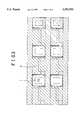
- FIG. 3is a diagram showing the shape of a lens-forming mask according to the present invention.
- a plurality of photodiodes 1are formed on a substrate while being spaced from one another by a predetermined distance, and a plurality of VCCDs 2 are formed on the substrate between the photodiodes 1.
- a lower planarizing layer 3 including a polyimide-based material having a superior heat-resistance which is a poly-condensate derived from an anhydride and aromatic thiamine to promerite acidis coated on the photodiodes 1, VCCDs 2 and exposed substrate. Then, as shown in FIG. 2B, the material of the polyimide group is thermally hardened at 200° C. to be solid. As shown in FIG.
- a photoresist 8is coated on the upper portion of the VCCDs 2 to be narrower than the VCCDs, and is subjected to an etching mask operation is performed via a photolitography.
- an isotropic etchingis performed to etch the lower planarizing layer 3 to be shaped as a plurality of hemispheric concave lenses.
- the photoresist 8is removed as shown in FIG. 2E.
- a dye layer of a highly polymerized compoundis subjected to a color spray and dyeing methods to form dye layers 4d, 4e, 4c and 4f in colors of magenta 4d, cyan 4e, yellow 4c and green 4f.
- the dye layeris stacked to increase overall CCD thickness as accumulating the colors.
- the CCD according to the present inventionadopts a method for forming the die layer in the lower planarizing layer 3, so that the total height of the CCD can be reduced so much.
- an upper planarizing layer 5is formed to perpendicularly focus incident light to the curvature of the concave lens formed by the dye layer 4 and the plane of the photodiodes 1 which is the light-receiving portion, and micro-lenses 6 are formed to have a curvature to perpendicularly focus the incident light to the photodiodes 1 as shown in FIG. 2H.
- the larger radius of curvatureis preferable in the micro-lenses 6 since the light-receivable range is enlarged, and a material constituting the micro-lens preferably has a smaller refractivity. Also, a materials constituting the upper planarizing layer 5 and dye layer 4 preferably have the refractivity larger than that of the micro-lens 6, in other words, more than 2.0.
- the radius of curvature of the concave lens in contact with the dye layer 4is smaller than that of the micro-lens 6 as compared with the area of the photodiode 1 which is the light-receiving portion.
- FIG. 3shows the mask pattern 9 according to the present invention, in which the corner of the rectangular mask is shaped as a triangle. Consequently, when the isotropic etching is performed to form the dye layers 4d, 4e, 4c and 4f, a hemispheric recesses are produced. By spraying colors into the recesses provide the layers of magenta 4d, cyan 4e, yellow 4c and green 4f, the color dye layer is completed.
- the incident lightadvances to the micro-lens 6 perpendicular to the upper planarizing layer 5, and the micro-lens 6 refracts and focuses the incident light in accordance with its own refractivity.
- the focused incident lightis refracted by the concave lens in contact with the dye layer 4.
- the refracted incident lightadvances perpendicular to the photodiode 1 to thereby reducing smear and maximizing sensitivity.
- the CCD image sensor and manufacturing method therefor as described aboveprovides a dye layer and a micro-lens that are lightweight and thin, thereby permitting enhanced miniaturization of a chip, i.e., higher density and higher integration of the chip.
- the lower planarizing layer 3, under the conventional color filter layeris formed as the hemispheric concave lens to involve the dye layer 4, so that the overall height from the micro-lens 6 to the photodiode 1 is lowered, thereby improving the transmissivity so much.
- the micro-lens(6 which is the uppermost layer) receives the light advancing perpendicular, with respect to the upper planarizing layer 5, to allow the light to be perpendicularly incident to the plane of the photodiode 1, thereby preventing the smear phenomenon of a picture and improving the sensitivity.
Landscapes
- Solid State Image Pick-Up Elements (AREA)
- Transforming Light Signals Into Electric Signals (AREA)
Abstract
Description
Claims (20)
Applications Claiming Priority (2)
| Application Number | Priority Date | Filing Date | Title |
|---|---|---|---|
| KR1019950016931AKR0151258B1 (en) | 1995-06-22 | 1995-06-22 | CD image sensor and its manufacturing method |
| KR16931/1995 | 1995-06-22 |
Publications (1)
| Publication Number | Publication Date |
|---|---|
| US5595930Atrue US5595930A (en) | 1997-01-21 |
Family
ID=19417921
Family Applications (1)
| Application Number | Title | Priority Date | Filing Date |
|---|---|---|---|
| US08/507,202Expired - LifetimeUS5595930A (en) | 1995-06-22 | 1995-07-26 | Method of manufacturing CCD image sensor by use of recesses |
Country Status (2)
| Country | Link |
|---|---|
| US (1) | US5595930A (en) |
| KR (1) | KR0151258B1 (en) |
Cited By (39)
| Publication number | Priority date | Publication date | Assignee | Title |
|---|---|---|---|---|
| US5888412A (en)* | 1996-03-04 | 1999-03-30 | Motorola, Inc. | Method for making a sculptured diaphragm |
| WO1999040624A1 (en)* | 1998-02-06 | 1999-08-12 | Shellcase Ltd. | Integrated circuit device |
| US6008843A (en)* | 1995-12-19 | 1999-12-28 | Lg Semicon Co., Ltd. | Color charge-coupled device |
| US6030852A (en)* | 1995-05-22 | 2000-02-29 | Matsushita Electronics Corporation | Solid-state imaging device and method of manufacturing the same |
| US6066511A (en)* | 1995-08-23 | 2000-05-23 | Sony Corporation | Manufacturing method for a solid state imaging device |
| US6171885B1 (en) | 1999-10-12 | 2001-01-09 | Taiwan Semiconductor Manufacturing Company | High efficiency color filter process for semiconductor array imaging devices |
| US6242277B1 (en)* | 1998-06-09 | 2001-06-05 | United Microelectronics Corp. | Method of fabricating a complementary metal-oxide semiconductor sensor device |
| US6251700B1 (en)* | 1998-06-16 | 2001-06-26 | United Microelectronics Corp. | Method of manufacturing complementary metal-oxide-semiconductor photosensitive device |
| US20020008767A1 (en)* | 2000-02-11 | 2002-01-24 | Do-Young Lee | Pixel layout for CMOS image sensor |
| US20030124763A1 (en)* | 2001-05-30 | 2003-07-03 | Taiwan Semiconductor Manufacturing Company | Colors only process to reduce package yield loss |
| US6737719B1 (en)* | 2002-10-25 | 2004-05-18 | Omnivision International Holding Ltd | Image sensor having combination color filter and concave-shaped micro-lenses |
| DE10301775A1 (en)* | 2003-01-18 | 2004-07-29 | Hentze-Lissotschenko Patentverwaltungs Gmbh & Co.Kg | Optical detector for objects, scanning device and confocal microscope includes second lens assembly comprising array of optical elements |
| US20040183185A1 (en)* | 1998-02-06 | 2004-09-23 | Avner Badihi | Packaged integrated circuits and methods of producing thereof |
| US20040251525A1 (en)* | 2003-06-16 | 2004-12-16 | Shellcase Ltd. | Methods and apparatus for packaging integrated circuit devices |
| US20050046001A1 (en)* | 2001-08-28 | 2005-03-03 | Tessera, Inc | High-frequency chip packages |
| US20050067681A1 (en)* | 2003-09-26 | 2005-03-31 | Tessera, Inc. | Package having integral lens and wafer-scale fabrication method therefor |
| US20050082654A1 (en)* | 2003-09-26 | 2005-04-21 | Tessera, Inc. | Structure and self-locating method of making capped chips |
| US20050101049A1 (en)* | 2003-11-12 | 2005-05-12 | Magnachip Semiconductor, Ltd. | Method for manufacturing CMOS image sensor |
| US20050104179A1 (en)* | 2003-07-03 | 2005-05-19 | Shellcase Ltd. | Methods and apparatus for packaging integrated circuit devices |
| US20050133688A1 (en)* | 2003-12-22 | 2005-06-23 | Jin Li | Layered lens structures and methods of production |
| US20050139984A1 (en)* | 2003-12-19 | 2005-06-30 | Tessera, Inc. | Package element and packaged chip having severable electrically conductive ties |
| WO2005071445A1 (en)* | 2004-01-23 | 2005-08-04 | Melexis Nv | Digital imaging device |
| US20050189635A1 (en)* | 2004-03-01 | 2005-09-01 | Tessera, Inc. | Packaged acoustic and electromagnetic transducer chips |
| US20060033131A1 (en)* | 2004-08-11 | 2006-02-16 | Dongbuanam Semiconductor Inc. | Complementary metal oxide semiconductor image sensor and method for fabricating the same |
| US20060073623A1 (en)* | 2004-09-30 | 2006-04-06 | Sharp Laboratories Of America, Inc. | Methods of forming a microlens array over a substrate employing a cmp stop |
| US20060169870A1 (en)* | 2005-02-01 | 2006-08-03 | Silsby Christopher D | Image sensor with embedded optical element |
| US20060267123A1 (en)* | 2005-05-27 | 2006-11-30 | Taiwan Semiconductor Manufacturing Company, Ltd. | Microlens Designs for CMOS Image Sensors |
| US20070034777A1 (en)* | 2005-08-12 | 2007-02-15 | Tessera, Inc. | Image sensor employing a plurality of photodetector arrays and/or rear-illuminated architecture |
| US20070145564A1 (en)* | 2005-03-22 | 2007-06-28 | Tessera, Inc. | Sequential fabrication of vertical conductive interconnects in capped chips |
| US20070145422A1 (en)* | 2005-12-28 | 2007-06-28 | Dong Bin Park | CMOS Image Sensor and Manufacturing Method Thereof |
| WO2007074977A1 (en)* | 2005-12-28 | 2007-07-05 | Siliconfile Technologies Inc. | Photodiode for image sensor and method of manufacturing the same |
| US20070190747A1 (en)* | 2006-01-23 | 2007-08-16 | Tessera Technologies Hungary Kft. | Wafer level packaging to lidded chips |
| US20070190691A1 (en)* | 2006-01-23 | 2007-08-16 | Tessera Technologies Hungary Kft. | Wafer level chip packaging |
| CN100345303C (en)* | 2002-08-01 | 2007-10-24 | 台湾积体电路制造股份有限公司 | Image sensor microlens group, image sensor and manufacturing method thereof |
| US20080002460A1 (en)* | 2006-03-01 | 2008-01-03 | Tessera, Inc. | Structure and method of making lidded chips |
| US20110193147A1 (en)* | 2010-02-05 | 2011-08-11 | Jung-Chak Ahn | Backside illumination cmos image sensors and methods of manufacturing the same |
| US8604605B2 (en) | 2007-01-05 | 2013-12-10 | Invensas Corp. | Microelectronic assembly with multi-layer support structure |
| US8987113B2 (en)* | 2004-09-13 | 2015-03-24 | Taiwan Semiconductor Manufacturing Company, Ltd. | Image sensor including multiple lenses and method of manufacture thereof |
| US10139619B2 (en) | 2015-02-12 | 2018-11-27 | Optiz, Inc. | Back side illumination image sensor with non-planar optical interface |
Families Citing this family (3)
| Publication number | Priority date | Publication date | Assignee | Title |
|---|---|---|---|---|
| KR20020042098A (en)* | 2000-11-30 | 2002-06-05 | 박종섭 | Image sensor and method for fabricating the same |
| KR20020057277A (en)* | 2000-12-30 | 2002-07-11 | 박종섭 | Image sensor having double lens and method for fabricating the same |
| KR20040000879A (en)* | 2002-06-26 | 2004-01-07 | 동부전자 주식회사 | Method for manufacturing cmos image sensor with uniformity topology |
Citations (6)
| Publication number | Priority date | Publication date | Assignee | Title |
|---|---|---|---|---|
| US4081277A (en)* | 1976-10-08 | 1978-03-28 | Eastman Kodak Company | Method for making a solid-state color imaging device having an integral color filter and the device |
| US4450475A (en)* | 1981-02-10 | 1984-05-22 | Matsushita Electric Industrial Co., Ltd. | Solid state color imaging apparatus |
| US4481530A (en)* | 1981-05-26 | 1984-11-06 | Agfa-Gevaert Aktiengesellschaft | Color filter arrangement for optoelectric converting devices |
| US5132251A (en)* | 1990-12-31 | 1992-07-21 | Samsung Electronics Co., Ltd. | Method for manufacturing a color filter |
| US5266501A (en)* | 1991-05-09 | 1993-11-30 | Kabushiki Kaisha Toshiba | Method for manufacturing a solid state image sensing device using transparent thermosetting resin layers |
| US5350490A (en)* | 1992-02-21 | 1994-09-27 | Samsung Electronics Ltd. | Forming a color filter on a semiconductor substrate |
- 1995
- 1995-06-22KRKR1019950016931Apatent/KR0151258B1/ennot_activeExpired - Lifetime
- 1995-07-26USUS08/507,202patent/US5595930A/ennot_activeExpired - Lifetime
Patent Citations (6)
| Publication number | Priority date | Publication date | Assignee | Title |
|---|---|---|---|---|
| US4081277A (en)* | 1976-10-08 | 1978-03-28 | Eastman Kodak Company | Method for making a solid-state color imaging device having an integral color filter and the device |
| US4450475A (en)* | 1981-02-10 | 1984-05-22 | Matsushita Electric Industrial Co., Ltd. | Solid state color imaging apparatus |
| US4481530A (en)* | 1981-05-26 | 1984-11-06 | Agfa-Gevaert Aktiengesellschaft | Color filter arrangement for optoelectric converting devices |
| US5132251A (en)* | 1990-12-31 | 1992-07-21 | Samsung Electronics Co., Ltd. | Method for manufacturing a color filter |
| US5266501A (en)* | 1991-05-09 | 1993-11-30 | Kabushiki Kaisha Toshiba | Method for manufacturing a solid state image sensing device using transparent thermosetting resin layers |
| US5350490A (en)* | 1992-02-21 | 1994-09-27 | Samsung Electronics Ltd. | Forming a color filter on a semiconductor substrate |
Cited By (102)
| Publication number | Priority date | Publication date | Assignee | Title |
|---|---|---|---|---|
| US6030852A (en)* | 1995-05-22 | 2000-02-29 | Matsushita Electronics Corporation | Solid-state imaging device and method of manufacturing the same |
| US6066511A (en)* | 1995-08-23 | 2000-05-23 | Sony Corporation | Manufacturing method for a solid state imaging device |
| US6008843A (en)* | 1995-12-19 | 1999-12-28 | Lg Semicon Co., Ltd. | Color charge-coupled device |
| US5888412A (en)* | 1996-03-04 | 1999-03-30 | Motorola, Inc. | Method for making a sculptured diaphragm |
| US20070013044A9 (en)* | 1998-02-06 | 2007-01-18 | Avner Badihi | Packaged integrated circuits and methods of producing thereof |
| WO1999040624A1 (en)* | 1998-02-06 | 1999-08-12 | Shellcase Ltd. | Integrated circuit device |
| US8592831B2 (en) | 1998-02-06 | 2013-11-26 | Invensas Corp. | Integrated circuit device |
| US20100323475A1 (en)* | 1998-02-06 | 2010-12-23 | Tessera Technologies Hungary Kft.. | Integrated circuit device |
| US7781240B2 (en) | 1998-02-06 | 2010-08-24 | Tessera Technologies Hungary Kft. | Integrated circuit device |
| US20070040180A1 (en)* | 1998-02-06 | 2007-02-22 | Tessera Technologies Hungary Kft. | Integrated circuit device |
| US20070042562A1 (en)* | 1998-02-06 | 2007-02-22 | Tessera Technologies Hungary Kft. | Integrated circuit device |
| US20030151124A1 (en)* | 1998-02-06 | 2003-08-14 | Shellcase, Ltd. | Integrated circuit device |
| US6646289B1 (en) | 1998-02-06 | 2003-11-11 | Shellcase Ltd. | Integrated circuit device |
| US7157742B2 (en) | 1998-02-06 | 2007-01-02 | Tessera Technologies Hungary Kft. | Integrated circuit device |
| US7408249B2 (en) | 1998-02-06 | 2008-08-05 | Tessera Technologies Hungary Kft. | Packaged integrated circuits and methods of producing thereof |
| US9530945B2 (en) | 1998-02-06 | 2016-12-27 | Invensas Corporation | Integrated circuit device |
| US20040183185A1 (en)* | 1998-02-06 | 2004-09-23 | Avner Badihi | Packaged integrated circuits and methods of producing thereof |
| US6242277B1 (en)* | 1998-06-09 | 2001-06-05 | United Microelectronics Corp. | Method of fabricating a complementary metal-oxide semiconductor sensor device |
| US6251700B1 (en)* | 1998-06-16 | 2001-06-26 | United Microelectronics Corp. | Method of manufacturing complementary metal-oxide-semiconductor photosensitive device |
| US6171885B1 (en) | 1999-10-12 | 2001-01-09 | Taiwan Semiconductor Manufacturing Company | High efficiency color filter process for semiconductor array imaging devices |
| US6274917B1 (en) | 1999-10-12 | 2001-08-14 | Taiwan Semiconductor Manufacturing Company | High efficiency color filter process for semiconductor array imaging devices |
| US20080217514A1 (en)* | 2000-02-11 | 2008-09-11 | Hyundai Electronics Industries Co., Ltd. | Pixel for CMOS Image Sensor Having a Select Shape for Low Pixel Crosstalk |
| US20020008767A1 (en)* | 2000-02-11 | 2002-01-24 | Do-Young Lee | Pixel layout for CMOS image sensor |
| US20060033828A1 (en)* | 2000-02-11 | 2006-02-16 | Hyundai Electronics Industries Co., Ltd. | Pixel for CMOS image sensor having a select shape for low pixel crosstalk |
| KR100752344B1 (en)* | 2000-02-11 | 2007-08-28 | 매그나칩 반도체 유한회사 | Pixel layout for cmos image sensor |
| US7057656B2 (en)* | 2000-02-11 | 2006-06-06 | Hyundai Electronics Industries Co., Ltd. | Pixel for CMOS image sensor having a select shape for low pixel crosstalk |
| US7816169B2 (en) | 2001-05-30 | 2010-10-19 | Taiwan Semiconductor Manufacturing Co., Ltd. | Colors only process to reduce package yield loss |
| US7183598B2 (en) | 2001-05-30 | 2007-02-27 | Taiwan Semiconductor Manufacturing Company | Colors only process to reduce package yield loss |
| US20050121737A1 (en)* | 2001-05-30 | 2005-06-09 | Yang-Tung Fan | Colors only process to reduce package yield loss |
| US6876049B2 (en)* | 2001-05-30 | 2005-04-05 | Taiwan Semiconductor Manufacturing Co. | Colors only process to reduce package yield loss |
| US20030124763A1 (en)* | 2001-05-30 | 2003-07-03 | Taiwan Semiconductor Manufacturing Company | Colors only process to reduce package yield loss |
| US7485906B2 (en) | 2001-05-30 | 2009-02-03 | Taiwan Semiconductor Manufacturing Company, Ltd. | Colors only process to reduce package yield loss |
| US20090111208A1 (en)* | 2001-05-30 | 2009-04-30 | Taiwan Semiconductor Manufacturing Co., Ltd. | Colors only process to reduce package yield loss |
| US20070120155A1 (en)* | 2001-05-30 | 2007-05-31 | Yang-Tung Fan | Colors only process to reduce package yield loss |
| US7566955B2 (en) | 2001-08-28 | 2009-07-28 | Tessera, Inc. | High-frequency chip packages |
| US20050046001A1 (en)* | 2001-08-28 | 2005-03-03 | Tessera, Inc | High-frequency chip packages |
| CN100345303C (en)* | 2002-08-01 | 2007-10-24 | 台湾积体电路制造股份有限公司 | Image sensor microlens group, image sensor and manufacturing method thereof |
| EP1414069A3 (en)* | 2002-10-25 | 2005-09-21 | OmniVision International Holding Ltd | Image sensor having combination color filter and concave-shaped micro-lenses |
| US6737719B1 (en)* | 2002-10-25 | 2004-05-18 | Omnivision International Holding Ltd | Image sensor having combination color filter and concave-shaped micro-lenses |
| US20040169843A1 (en)* | 2003-01-18 | 2004-09-02 | Aleksei Mikhailov | Detection apparatus for the optical detection of an object, method for operating a detection apparatus of this type and scanning apparatus and confocal microscope |
| US7015450B2 (en) | 2003-01-18 | 2006-03-21 | Hentze-Lissotschenko Patentverwaltungs Gmbh Co. Kg | Detection apparatus for the optical detection of an object, method for operating a detection apparatus of this type and scanning apparatus and confocal microscope |
| DE10301775A1 (en)* | 2003-01-18 | 2004-07-29 | Hentze-Lissotschenko Patentverwaltungs Gmbh & Co.Kg | Optical detector for objects, scanning device and confocal microscope includes second lens assembly comprising array of optical elements |
| US7642629B2 (en) | 2003-06-16 | 2010-01-05 | Tessera Technologies Hungary Kft. | Methods and apparatus for packaging integrated circuit devices |
| US6972480B2 (en) | 2003-06-16 | 2005-12-06 | Shellcase Ltd. | Methods and apparatus for packaging integrated circuit devices |
| US20050205977A1 (en)* | 2003-06-16 | 2005-09-22 | Shellcase Ltd. | Methods and apparatus for packaging integrated circuit devices |
| US7265440B2 (en) | 2003-06-16 | 2007-09-04 | Tessera Technologies Hungary Kft. | Methods and apparatus for packaging integrated circuit devices |
| US20040251525A1 (en)* | 2003-06-16 | 2004-12-16 | Shellcase Ltd. | Methods and apparatus for packaging integrated circuit devices |
| US7479398B2 (en) | 2003-07-03 | 2009-01-20 | Tessera Technologies Hungary Kft. | Methods and apparatus for packaging integrated circuit devices |
| US7495341B2 (en) | 2003-07-03 | 2009-02-24 | Tessera Technologies Hungary Kft. | Methods and apparatus for packaging integrated circuit devices |
| US20070138498A1 (en)* | 2003-07-03 | 2007-06-21 | Tessera Technologies Hungary Kft. | Methods and apparatus for packaging integrated circuit devices |
| US20050104179A1 (en)* | 2003-07-03 | 2005-05-19 | Shellcase Ltd. | Methods and apparatus for packaging integrated circuit devices |
| US7192796B2 (en) | 2003-07-03 | 2007-03-20 | Tessera Technologies Hungary Kft. | Methods and apparatus for packaging integrated circuit devices |
| US20050082654A1 (en)* | 2003-09-26 | 2005-04-21 | Tessera, Inc. | Structure and self-locating method of making capped chips |
| US20050067681A1 (en)* | 2003-09-26 | 2005-03-31 | Tessera, Inc. | Package having integral lens and wafer-scale fabrication method therefor |
| US20080032457A1 (en)* | 2003-09-26 | 2008-02-07 | Tessera, Inc. | Structure and method of making sealed capped chips |
| US20050087861A1 (en)* | 2003-09-26 | 2005-04-28 | Tessera, Inc. | Back-face and edge interconnects for lidded package |
| US20070096312A1 (en)* | 2003-09-26 | 2007-05-03 | Tessera, Inc. | Structure and self-locating method of making capped chips |
| US20070096311A1 (en)* | 2003-09-26 | 2007-05-03 | Tessera, Inc. | Structure and method of making capped chips having vertical interconnects |
| US7224056B2 (en) | 2003-09-26 | 2007-05-29 | Tessera, Inc. | Back-face and edge interconnects for lidded package |
| US20050095835A1 (en)* | 2003-09-26 | 2005-05-05 | Tessera, Inc. | Structure and method of making capped chips having vertical interconnects |
| US7163832B2 (en)* | 2003-11-12 | 2007-01-16 | Magnachip Semiconductor Ltd. | Method for manufacturing CMOS image sensor |
| US20050101049A1 (en)* | 2003-11-12 | 2005-05-12 | Magnachip Semiconductor, Ltd. | Method for manufacturing CMOS image sensor |
| US20050139984A1 (en)* | 2003-12-19 | 2005-06-30 | Tessera, Inc. | Package element and packaged chip having severable electrically conductive ties |
| US7365305B2 (en) | 2003-12-22 | 2008-04-29 | Micron Technology, Inc. | Layered lens structures and methods of production in which radius of curvature of the upper lens can be varied |
| US7205526B2 (en)* | 2003-12-22 | 2007-04-17 | Micron Technology, Inc. | Methods of fabricating layered lens structures |
| US20060289723A1 (en)* | 2003-12-22 | 2006-12-28 | Jin Li | Layered microlens structures and devices |
| US20050133688A1 (en)* | 2003-12-22 | 2005-06-23 | Jin Li | Layered lens structures and methods of production |
| US20060027734A1 (en)* | 2003-12-22 | 2006-02-09 | Jin Li | Layered microlens structures and devices |
| US7199347B2 (en)* | 2003-12-22 | 2007-04-03 | Micron Technology, Inc. | Layered microlens structures and devices |
| US20110180695A1 (en)* | 2003-12-22 | 2011-07-28 | Round Rock Research, Llc | Layered lens structures and methods of production |
| US20070096016A1 (en)* | 2003-12-22 | 2007-05-03 | Jin Li | Layered lens structures and methods of production |
| WO2005071445A1 (en)* | 2004-01-23 | 2005-08-04 | Melexis Nv | Digital imaging device |
| US20050189635A1 (en)* | 2004-03-01 | 2005-09-01 | Tessera, Inc. | Packaged acoustic and electromagnetic transducer chips |
| US20050189622A1 (en)* | 2004-03-01 | 2005-09-01 | Tessera, Inc. | Packaged acoustic and electromagnetic transducer chips |
| US20070120163A1 (en)* | 2004-08-11 | 2007-05-31 | Dongbu Electronics Co. Ltd. | Complementary metal oxide semiconductor image sensor and method for fabricating the same |
| US20060033131A1 (en)* | 2004-08-11 | 2006-02-16 | Dongbuanam Semiconductor Inc. | Complementary metal oxide semiconductor image sensor and method for fabricating the same |
| US7166489B2 (en)* | 2004-08-11 | 2007-01-23 | Dongbu Electronics Co., Ltd. | Complementary metal oxide semiconductor image sensor and method for fabricating the same |
| US7427799B2 (en) | 2004-08-11 | 2008-09-23 | Dongbu Electronics Co., Ltd. | Complementary metal oxide semiconductor image sensor and method for fabricating the same |
| US8987113B2 (en)* | 2004-09-13 | 2015-03-24 | Taiwan Semiconductor Manufacturing Company, Ltd. | Image sensor including multiple lenses and method of manufacture thereof |
| US9768224B2 (en) | 2004-09-13 | 2017-09-19 | Taiwan Semiconductor Manufacturing Company, Ltd. | Image sensor including multiple lenses and method of manufacture thereof |
| US20060073623A1 (en)* | 2004-09-30 | 2006-04-06 | Sharp Laboratories Of America, Inc. | Methods of forming a microlens array over a substrate employing a cmp stop |
| US7029944B1 (en)* | 2004-09-30 | 2006-04-18 | Sharp Laboratories Of America, Inc. | Methods of forming a microlens array over a substrate employing a CMP stop |
| US20060169870A1 (en)* | 2005-02-01 | 2006-08-03 | Silsby Christopher D | Image sensor with embedded optical element |
| GB2423416A (en)* | 2005-02-01 | 2006-08-23 | Agilent Technologies Inc | Image sensor with embedded optical element |
| US8143095B2 (en) | 2005-03-22 | 2012-03-27 | Tessera, Inc. | Sequential fabrication of vertical conductive interconnects in capped chips |
| US20070145564A1 (en)* | 2005-03-22 | 2007-06-28 | Tessera, Inc. | Sequential fabrication of vertical conductive interconnects in capped chips |
| US20060267123A1 (en)* | 2005-05-27 | 2006-11-30 | Taiwan Semiconductor Manufacturing Company, Ltd. | Microlens Designs for CMOS Image Sensors |
| US7196388B2 (en) | 2005-05-27 | 2007-03-27 | Taiwan Semiconductor Manufacturing Company, Ltd. | Microlens designs for CMOS image sensors |
| US7566853B2 (en) | 2005-08-12 | 2009-07-28 | Tessera, Inc. | Image sensor employing a plurality of photodetector arrays and/or rear-illuminated architecture |
| US20070034777A1 (en)* | 2005-08-12 | 2007-02-15 | Tessera, Inc. | Image sensor employing a plurality of photodetector arrays and/or rear-illuminated architecture |
| US20070145422A1 (en)* | 2005-12-28 | 2007-06-28 | Dong Bin Park | CMOS Image Sensor and Manufacturing Method Thereof |
| WO2007074977A1 (en)* | 2005-12-28 | 2007-07-05 | Siliconfile Technologies Inc. | Photodiode for image sensor and method of manufacturing the same |
| US20070190747A1 (en)* | 2006-01-23 | 2007-08-16 | Tessera Technologies Hungary Kft. | Wafer level packaging to lidded chips |
| US20070190691A1 (en)* | 2006-01-23 | 2007-08-16 | Tessera Technologies Hungary Kft. | Wafer level chip packaging |
| US7936062B2 (en) | 2006-01-23 | 2011-05-03 | Tessera Technologies Ireland Limited | Wafer level chip packaging |
| US20080002460A1 (en)* | 2006-03-01 | 2008-01-03 | Tessera, Inc. | Structure and method of making lidded chips |
| US20080029879A1 (en)* | 2006-03-01 | 2008-02-07 | Tessera, Inc. | Structure and method of making lidded chips |
| US8604605B2 (en) | 2007-01-05 | 2013-12-10 | Invensas Corp. | Microelectronic assembly with multi-layer support structure |
| US9548145B2 (en) | 2007-01-05 | 2017-01-17 | Invensas Corporation | Microelectronic assembly with multi-layer support structure |
| US20110193147A1 (en)* | 2010-02-05 | 2011-08-11 | Jung-Chak Ahn | Backside illumination cmos image sensors and methods of manufacturing the same |
| US8541857B2 (en)* | 2010-02-05 | 2013-09-24 | Samsung Electronics Co., Ltd. | Backside illumination CMOS image sensors and methods of manufacturing the same |
| US10139619B2 (en) | 2015-02-12 | 2018-11-27 | Optiz, Inc. | Back side illumination image sensor with non-planar optical interface |
Also Published As
| Publication number | Publication date |
|---|---|
| KR970004051A (en) | 1997-01-29 |
| KR0151258B1 (en) | 1998-10-01 |
Similar Documents
| Publication | Publication Date | Title |
|---|---|---|
| US5595930A (en) | Method of manufacturing CCD image sensor by use of recesses | |
| US5672519A (en) | Method of fabricating solid state image sensing elements | |
| US8390931B2 (en) | Micro-lenses for CMOS imagers and method for manufacturing micro-lenses | |
| US5493143A (en) | Solid color image pickup device | |
| US8795559B2 (en) | Method for forming imagers | |
| US6818934B1 (en) | Image sensor having micro-lens array separated with trench structures and method of making | |
| US6737719B1 (en) | Image sensor having combination color filter and concave-shaped micro-lenses | |
| US6417022B1 (en) | Method for making long focal length micro-lens for color filters | |
| JP2004235635A (en) | Method for manufacturing CMOS image sensor | |
| US7352511B2 (en) | Micro-lenses for imagers | |
| KR100278983B1 (en) | Solid state imaging device | |
| JP2841037B2 (en) | Manufacturing method of CCD solid-state imaging device | |
| US6699729B1 (en) | Method of forming planar color filters in an image sensor | |
| US7553689B2 (en) | Semiconductor device with micro-lens and method of making the same | |
| US6608358B1 (en) | Dummy pattern for improving micro-lens formation in an image sensor | |
| US20050208432A1 (en) | Methods of forming a microlens array over a substrate | |
| US20040082096A1 (en) | Method for forming an image sensor having concave-shaped micro-lenses | |
| CN100405607C (en) | Image sensor having microlenses separated by ridge structures and method of manufacturing the same | |
| US6800838B2 (en) | Image sensor having reduced stress color filters and method of making | |
| US20040080006A1 (en) | Image sensor having concave-shaped micro-lenses | |
| JP3516459B2 (en) | Method for manufacturing solid-state imaging device | |
| KR0156118B1 (en) | The fabrication method of solid state image sensor | |
| KR100259066B1 (en) | Solid state imaging device manufacturing method | |
| KR100829379B1 (en) | Image sensor manufacturing method | |
| KR20030001098A (en) | Method of fabricating solid state image sensor |
Legal Events
| Date | Code | Title | Description |
|---|---|---|---|
| AS | Assignment | Owner name:LG SEMICON CO., LTD., KOREA, REPUBLIC OF Free format text:ASSIGNMENT OF ASSIGNORS INTEREST;ASSIGNOR:BAEK, EUY HYEON;REEL/FRAME:007708/0459 Effective date:19950812 | |
| STCF | Information on status: patent grant | Free format text:PATENTED CASE | |
| FEPP | Fee payment procedure | Free format text:PAYOR NUMBER ASSIGNED (ORIGINAL EVENT CODE: ASPN); ENTITY STATUS OF PATENT OWNER: LARGE ENTITY | |
| FPAY | Fee payment | Year of fee payment:4 | |
| FPAY | Fee payment | Year of fee payment:8 | |
| AS | Assignment | Owner name:HYNIX SEMICONDUCTOR INC., KOREA, REPUBLIC OF Free format text:CHANGE OF NAME;ASSIGNOR:GOLDSTAR ELECTRON CO., LTD;REEL/FRAME:015232/0847 Effective date:19950201 | |
| AS | Assignment | Owner name:MAGNACHIP SEMICONDUCTOR, LTD., KOREA, REPUBLIC OF Free format text:ASSIGNMENT OF ASSIGNORS INTEREST;ASSIGNOR:HYNIX SEMICONDUCTOR, INC.;REEL/FRAME:016216/0649 Effective date:20041004 | |
| AS | Assignment | Owner name:U.S. BANK NATIONAL ASSOCIATION, AS COLLATERAL TRUS Free format text:SECURITY INTEREST;ASSIGNOR:MAGNACHIP SEMICONDUCTOR, LTD.;REEL/FRAME:016470/0530 Effective date:20041223 | |
| FPAY | Fee payment | Year of fee payment:12 | |
| AS | Assignment | Owner name:HYUNDAI MICRO ELECTRONICS CO., LTD. (BRANCH OFFICE Free format text:CORRECTIVE ASSIGNMENT TO CORRECT THE CONVEYING PARTY, RECEIVING PARTY AND EXECUTION DATE PREVIOUSLY RECORDED ON REEL 015232 FRAME 0847;ASSIGNOR:LG SEMICON CO., LTD;REEL/FRAME:022689/0679 Effective date:19990726 | |
| AS | Assignment | Owner name:HYUNDAI ELECTRONICS INDUSTRIES CO., LTD., GEORGIA Free format text:MERGER;ASSIGNOR:HYUNDAI MICRO ELECTRONICS CO., LTD.;REEL/FRAME:022742/0478 Effective date:19991014 Owner name:HYNIX SEMICONDUCTOR INC., KOREA, REPUBLIC OF Free format text:CHANGE OF NAME;ASSIGNOR:HYUNDAI ELECTRONICS INDUSTRIES CO., LTD.;REEL/FRAME:022742/0555 Effective date:20010329 | |
| AS | Assignment | Owner name:HYUNDAI ELECTRONICS INDUSTRIES CO., LTD., KOREA, R Free format text:CORRECTIVE ASSIGNMENT TO CORRECT THE COUNTRY IN THE ADDRESS OF THE RECEIVING PARTY PREVIOUSLY RECORDED ON REEL 022742 FRAME 0478;ASSIGNOR:HYUNDAI MICRO ELECTRONICS CO., LTD.;REEL/FRAME:022746/0279 Effective date:19991014 | |
| AS | Assignment | Owner name:MAGNACHIP SEMICONDUCTOR, LTD., KOREA, REPUBLIC OF Free format text:PARTIAL RELEASE OF SECURITY INTEREST;ASSIGNOR:U.S. BANK NATIONAL ASSOCIATION, AS COLLATERAL TRUSTEE;REEL/FRAME:022746/0870 Effective date:20090527 Owner name:CROSSTEK CAPITAL, LLC, DELAWARE Free format text:ASSIGNMENT OF ASSIGNORS INTEREST;ASSIGNOR:MAGNACHIP SEMICONDUCTOR, LTD.;REEL/FRAME:022764/0270 Effective date:20090514 Owner name:CROSSTEK CAPITAL, LLC,DELAWARE Free format text:ASSIGNMENT OF ASSIGNORS INTEREST;ASSIGNOR:MAGNACHIP SEMICONDUCTOR, LTD.;REEL/FRAME:022764/0270 Effective date:20090514 | |
| AS | Assignment | Owner name:INTELLECTUAL VENTURES II LLC, DELAWARE Free format text:MERGER;ASSIGNOR:CROSSTEK CAPITAL, LLC;REEL/FRAME:026637/0632 Effective date:20110718 |