US5595602A - Diffuser for uniform gas distribution in semiconductor processing and method for using the same - Google Patents
Diffuser for uniform gas distribution in semiconductor processing and method for using the sameDownload PDFInfo
- Publication number
- US5595602A US5595602AUS08/514,634US51463495AUS5595602AUS 5595602 AUS5595602 AUS 5595602AUS 51463495 AUS51463495 AUS 51463495AUS 5595602 AUS5595602 AUS 5595602A
- Authority
- US
- United States
- Prior art keywords
- porous sintered
- gas
- plate
- chamber
- providing
- Prior art date
- Legal status (The legal status is an assumption and is not a legal conclusion. Google has not performed a legal analysis and makes no representation as to the accuracy of the status listed.)
- Expired - Lifetime
Links
Images

Classifications
- C—CHEMISTRY; METALLURGY
- C23—COATING METALLIC MATERIAL; COATING MATERIAL WITH METALLIC MATERIAL; CHEMICAL SURFACE TREATMENT; DIFFUSION TREATMENT OF METALLIC MATERIAL; COATING BY VACUUM EVAPORATION, BY SPUTTERING, BY ION IMPLANTATION OR BY CHEMICAL VAPOUR DEPOSITION, IN GENERAL; INHIBITING CORROSION OF METALLIC MATERIAL OR INCRUSTATION IN GENERAL
- C23C—COATING METALLIC MATERIAL; COATING MATERIAL WITH METALLIC MATERIAL; SURFACE TREATMENT OF METALLIC MATERIAL BY DIFFUSION INTO THE SURFACE, BY CHEMICAL CONVERSION OR SUBSTITUTION; COATING BY VACUUM EVAPORATION, BY SPUTTERING, BY ION IMPLANTATION OR BY CHEMICAL VAPOUR DEPOSITION, IN GENERAL
- C23C16/00—Chemical coating by decomposition of gaseous compounds, without leaving reaction products of surface material in the coating, i.e. chemical vapour deposition [CVD] processes
- C23C16/44—Chemical coating by decomposition of gaseous compounds, without leaving reaction products of surface material in the coating, i.e. chemical vapour deposition [CVD] processes characterised by the method of coating
- C23C16/455—Chemical coating by decomposition of gaseous compounds, without leaving reaction products of surface material in the coating, i.e. chemical vapour deposition [CVD] processes characterised by the method of coating characterised by the method used for introducing gases into reaction chamber or for modifying gas flows in reaction chamber
- C23C16/45563—Gas nozzles
- C23C16/45568—Porous nozzles
- C—CHEMISTRY; METALLURGY
- C23—COATING METALLIC MATERIAL; COATING MATERIAL WITH METALLIC MATERIAL; CHEMICAL SURFACE TREATMENT; DIFFUSION TREATMENT OF METALLIC MATERIAL; COATING BY VACUUM EVAPORATION, BY SPUTTERING, BY ION IMPLANTATION OR BY CHEMICAL VAPOUR DEPOSITION, IN GENERAL; INHIBITING CORROSION OF METALLIC MATERIAL OR INCRUSTATION IN GENERAL
- C23C—COATING METALLIC MATERIAL; COATING MATERIAL WITH METALLIC MATERIAL; SURFACE TREATMENT OF METALLIC MATERIAL BY DIFFUSION INTO THE SURFACE, BY CHEMICAL CONVERSION OR SUBSTITUTION; COATING BY VACUUM EVAPORATION, BY SPUTTERING, BY ION IMPLANTATION OR BY CHEMICAL VAPOUR DEPOSITION, IN GENERAL
- C23C16/00—Chemical coating by decomposition of gaseous compounds, without leaving reaction products of surface material in the coating, i.e. chemical vapour deposition [CVD] processes
- C23C16/44—Chemical coating by decomposition of gaseous compounds, without leaving reaction products of surface material in the coating, i.e. chemical vapour deposition [CVD] processes characterised by the method of coating
- C23C16/455—Chemical coating by decomposition of gaseous compounds, without leaving reaction products of surface material in the coating, i.e. chemical vapour deposition [CVD] processes characterised by the method of coating characterised by the method used for introducing gases into reaction chamber or for modifying gas flows in reaction chamber
Definitions
- the present inventionrelates generally to semiconductor processing, and more specifically to a method for uniformly distributing gas in a closed chamber.
- plasma reactor equipmentis employed for depositing layers or films of conductive material, semiconductor material, or insulating materials in various patterns, configurations, and thicknesses to form microcircuits. Dry etching of semiconductor materials can also be conducted with chemical vapor transport systems to selectively remove desired areas of such materials to form the requisite patterns or configurations.
- the use of these aforementioned equipmentoften requires various gases to be introduced into a contained environment into which a semiconductor wafer has been placed to form microcircuits.
- the contained environmentis a plasma chamber of the equipment.
- the gasis desired to be uniformly distributed over the surface of the semiconductor wafer inside the chamber for purposes of deposition, etch, or another wafer fabrication process.
- the reason for desiring uniform gas distributionis that variations in the gas flow across the surface of the wafer result in nonuniform deposition or etch causing nonplanar topography which can lead to yield loss, incomplete etch, and consequently device failures.
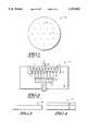
- FIG. 1One such gas dispersion disk is shown in FIG. 1, wherein the disk 10 has a plurality of holes 12 in the disk.
- the holes 12are in practice drilled in precise locations per a specific hole pattern.
- the specific hole patternsare proprietary to each semiconductor device manufacturer because the hole patterns are typically experimentally determined to yield the most uniform gas distribution for that company's plasma reactor equipment configuration.
- FIG. 2is a cross-sectional schematic of a plasma reactor 14.
- the plasma reactor 14has a reactor chamber 16 which contains a semiconductor wafer 18 supported by a susceptor or pedestal 20. There is a gas inlet 22 at the top of the reactor chamber 16.
- the incoming gasis dispersed through two gas dispersion disks, wherein the top disk 10 will be referred to as a blocker plate or a pre-diffuser, and the bottom disk 24 will be referred to as a face plate or electrode.
- the holes 26 in the face plate 24are tapered, as illustrated, to better disperse the gas exiting holes 26 which are themselves positioned above the surface of the semiconductor wafer 18.
- the holescan be counterbored such that the top portion of holes are larger than the bottom portion at the exit surface.
- This gas dispersion techniquehas several disadvantages.
- One disadvantageis that these plates with the company proprietary hole patterns are very expensive due to the manufacturing process required to drill the holes. Furthermore, these plates are often made of anodized aluminum for increased life, and the anodization process itself is costly.
- an increase in the diameter of the semiconductor waferexacerbates the nonuniform flow problems especially at the edges of the wafer. For example, the gas flow may be laminar at the center of the wafer surface but is turbulent at the edges. Furthermore, process drift occurs over time and the flow pattern changes leading to variability in the process. In addition, the holes clog after a time in manufacturing leading to undesirable flow patterns and results.
- FIG. 1illustrates, in a top view, a gas dispersion disk having a pattern of holes as known in the prior art.
- FIG. 2illustrates, in cross-section, a schematic of a plasma chamber having a two-stage gas dispersion, as the typical prior art method for gas distribution.
- FIG. 3illustrates, in cross-section, a diffuser for uniform gas distribution in semiconductor processing in accordance with an embodiment of the invention.
- FIG. 4illustrates, in cross-section, a diffuser composed of two layers of materials having different porosities for uniform gas distribution in semiconductor processing in another embodiment of the invention.
- FIG. 5illustrates, in cross-section, a schematic of a plasma chamber utilizing the diffuser of FIG. 3, in accordance with a method of using the diffuser to uniformly distribute incoming gas for semiconductor processing.
- FIG. 6illustrates, in cross-section, a schematic of a closed chamber utilizing the diffuser of FIG. 3, in an alternative method of using the diffuser to uniformly distribute incoming gas.
- the inventionprovides a method for uniformly distributing a gas flow into an enclosed environment, such as a plasma chamber of CVD equipment, for semiconductor processing applications.
- the methodinvolves using a porous sintered plate having a preselected porosity and thickness as a gas diffuser.
- the porous sintered plateis positioned in the CVD equipment between the gas inlet and the surface of a semiconductor wafer such that the incoming gas must flow through the porous sintered plate.
- the incoming gasis uniformly diffused through the thickness of the sintered plate due to its porous nature.
- the gasis uniformly distributed such that laminar flow is maintained across the entire surface of the porous sintered plate.
- the semiconductor waferis supported by a pedestal or susceptor set a predetermined distance away from the bottom surface of the porous sintered plate.
- the incoming gas necessary for the preselected semiconductor processis uniformly distributed over the surface of the semiconductor wafer for the applicable semiconductor process.
- FIGS. 3 and 4illustrate, in cross-section, two embodiments of a diffuser for uniformly distributing gas in semiconductor processing in accordance with the present invention.
- the gas diffuser plate 30is composed of a porous sintered material. Examples of suitable materials include, but are not limited to, stainless steel, aluminum, nickel, ceramic, and any alloy thereof. Sintered metals are preferable over ceramics for a CVD environment, whereas ceramics are more desirable in etch or a magnetically enhanced environment.
- a major difference and advantage of the present diffuser 30 over the prior artis that there are no holes required to disperse incoming gas.
- the porosity of the sintered plateintrinsically distributes the gas through the plate in a uniform fashion.
- the elimination of the holesmeans that specific company proprietary hole patterns are avoided. Furthermore, fluid dynamic modeling and experimentation of different hole patterns for a particular plate size to achieve laminar flow are eliminated. Additionally, the prohibitively expensive cost of drilling particular patterns of small holes, especially tapered holes, is eliminated.
- the gas diffuser plate 30 of the present inventionis manufactured through a sintering process, that allows one to control the desired porosity of the final sintered product. It is important that the sintering process produces a final product that is homogeneously porous for uniform diffusion. It is expected that a porosity ranging from 0.2 ⁇ m to 5 ⁇ m would be most applicable in the field of semiconductor processing, where the relevant processes requiring laminar gas flow include CVD, etch, and implant. For example, the etching process requires a smaller porosity than does deposition of tetraethyl orthosilicate (TEOS), both in the submicron range, while implanting can be performed with relatively large pore sizes, in the micron range.
- TEOStetraethyl orthosilicate
- a sandwich of two different porosity layersis used to form a gas diffuser plate 32.
- This multilayer gas diffuser 32may either be a single sintered product having two layers of porous materials, or it may be two separate single layer diffusers used in conjunction with each other to further diffuse the incoming gas through the diffuser 32.
- the different layers of materialshave different predetermined porosity levels.
- the top layer 34may have a predetermined porosity level of 0.2 ⁇ m while the bottom layer 36 may have a predetermined porosity level of 0.5 to 5 ⁇ m.
- top layer 34can be thinner than the bottom layer 34, although it is not a requirement in practicing the present invention.
- a 1.6 mm (0.0625 inch) layermay suffice for top layer 34 while a 3.2 mm (0.125 inch) layer may suffice for bottom layer 36.
- FIG. 4only illustrates two layers of porous materials used to form a multilayer gas diffuser, it should be understood that additional layers of different porosities may be added to the gas diffuser to achieve the desired diffusive effect to obtain laminar flow.
- additional layers of different porositiesmay be added to the gas diffuser to achieve the desired diffusive effect to obtain laminar flow.
- the surface area requiring laminar gas flowis very large, substantially larger than either 8 inch to 10 inch (200 to 250 mm) wafers, it may be necessary to add more porous layers to achieve the desired laminar flow because increases in surface area exacerbates the fluid flow problems around the edges of the area.
- a single layer gas diffuser plate having a first porosityas a blocker plate and an additional single layer or multilayer gas diffuser having a different porosity as a face plate
- a multilayer gas diffusercan also be used as a blocker plate.
- different materials combinationsare also possible in practicing the invention.
- a sintered metal blocker platecould be used in conjunction with a ceramic face plate, or vice versa.
- two different type of sintered metals or sintered metal alloyscan be used for the blocker plate and face plate.
- FIG. 5illustrates, in cross-section, a schematic of a plasma chamber utilizing the diffuser of FIG. 3, in accordance with a method of using the diffuser to uniformly distribute incoming gas for semiconductor processing.
- the diffuser 30is placed in the top portion of the plasma chamber such that the gas inlet must introduce the incoming gas through the diffuser 30.
- the diffuser 30is a porous sintered disk, so that there are voids within the material itself. There is no hole pattern associated with this diffuser. Instead, the voids are substantially homogeneously distributed within the diffuser plate itself by virtue of the porous nature of the sintered material. In this manner, incoming gas is distributed through the diffuser by flowing through the voids in within the diffuser.
- the semiconductor wafer 18is supported by susceptor or pedestal 20 within the plasma chamber.
- the susceptor 20is a standard fixture within either the CVD or etch equipment themselves.
- a major advantage to incorporating the use of the diffuser 30 in a CVD processis the uniform distribution of the incoming gas across the surface of the semiconductor wafer.
- the flowis laminar across the entire surface of the diffuser, even across a large surface area, whereas the prior art method of using a pattern of holes means that as the surface area of disk increases, the hole pattern must be changed in order to maintain some uniformity in the flow.
- changing the hole patternwould require remodeling of the fluid dynamics which would still not yield as uniform of a flow as the porous sintered diffuser of the present invention.
- An additional benefit of utilizing the porous sintered diffuser in the present methodis that the incoming gas is also filtered for particulates, leading to cleaner gas for the vapor deposition or etch processes.
- the diffuser 30 or 32is in no way limited to a CVD process, because the diffuser 30 can also be used in an etch process.
- Typical etch equipmentrequires multiple baffles having specific hole patterns to achieve uniform gas flow, similar to the CVD equipment using multistage gas dispersion disks, which poses serious fluid modeling and aligning of multiple baffles problems.
- using the diffuser 30 of the present invention in an etch processwill greatly simplify the etch process while providing laminar gas flow with no alignment difficulties, regardless of how many baffles are required.
- FIG. 6illustrates, in cross-section, a schematic of a closed chamber utilizing the diffuser of FIG. 3, in an alternative method of using the diffuser to uniformly distribute incoming gas.
- the diffuseris placed outside of the chamber but the gas inlet is still positioned such that the incoming gas must pass through the diffuser before entering the chamber.
- Thisis an effective and non-disruptive method of introducing gas into any vacuum chamber.
- This method of practicing the present inventionenables a low velocity, high volume flow which is key in providing minimal disruption of particulate matter within the chamber.
- the operation of the gas diffuseris the same as discussed above.
- This particular configuration, wherein the diffuser is mounted outside of the chambermay be more desirable when the chamber is small due to the space constraint.
- a multilayer diffuserhaving different porosity layers, different materials, or any combination thereof, may also be used in conjunction with this embodiment to provide uniform gas flow through the diffuser into the chamber.
- a porous sintered platemay be used as a gas diffuser in a semiconductor process where laminar gas flow over a semiconductor wafer is required.
- the porosity of the gas diffusermay be varied depending on the particular process requirements and the size of the surface area of the semiconductor wafer.
- the present inventioneliminates the expensive tapered hole drilling process, as well as the use of any particular hole pattern, whether proprietary or not.
- particulatesare pre-filtered out of the incoming gas as an added benefit.
- the low velocity flow afforded by practicing the present inventionminimizes the disruption of the particulates already present inside the closed chamber.
- the gas diffuseris easy to implement across a wide variety of semiconductor processes and equipment.
- the gas diffusermay be a simple plate that is assembled into a clamp ring for attachment to a CVD chamber, or the gas diffuser may be constructed as a single unit having a clamp ring integrally made with the diffuser.
- the inventionis not limited to a deposition process, but may also be used in conjunction with an etch process, or any other semiconductor manufacturing process where uniform or laminar gas flow is required. It is also important to note that the present invention is not limited in any way to any particular type of semiconductor equipment but may rather be used in conjunction with any closed chamber where the gas diffuser may be fitted below the gas inlet. Furthermore, in the multilayer gas diffuser configuration, the various layers may abut each other or they may be separated by an air gap. A separation between layers should pose no alignment problems as experienced in the prior art because there are no hole patterns to align since all layers are presumed to be homogeneously porous within each layer. Therefore, it is intended that this invention encompasses all such variations and modifications falling within the scope of the appended claims.
Landscapes
- Chemical & Material Sciences (AREA)
- General Chemical & Material Sciences (AREA)
- Chemical Kinetics & Catalysis (AREA)
- Engineering & Computer Science (AREA)
- Materials Engineering (AREA)
- Mechanical Engineering (AREA)
- Metallurgy (AREA)
- Organic Chemistry (AREA)
- Drying Of Semiconductors (AREA)
Abstract
Description
Claims (18)
Priority Applications (1)
| Application Number | Priority Date | Filing Date | Title |
|---|---|---|---|
| US08/514,634US5595602A (en) | 1995-08-14 | 1995-08-14 | Diffuser for uniform gas distribution in semiconductor processing and method for using the same |
Applications Claiming Priority (1)
| Application Number | Priority Date | Filing Date | Title |
|---|---|---|---|
| US08/514,634US5595602A (en) | 1995-08-14 | 1995-08-14 | Diffuser for uniform gas distribution in semiconductor processing and method for using the same |
Publications (1)
| Publication Number | Publication Date |
|---|---|
| US5595602Atrue US5595602A (en) | 1997-01-21 |
Family
ID=24048059
Family Applications (1)
| Application Number | Title | Priority Date | Filing Date |
|---|---|---|---|
| US08/514,634Expired - LifetimeUS5595602A (en) | 1995-08-14 | 1995-08-14 | Diffuser for uniform gas distribution in semiconductor processing and method for using the same |
Country Status (1)
| Country | Link |
|---|---|
| US (1) | US5595602A (en) |
Cited By (34)
| Publication number | Priority date | Publication date | Assignee | Title |
|---|---|---|---|---|
| US5906683A (en)* | 1996-04-16 | 1999-05-25 | Applied Materials, Inc. | Lid assembly for semiconductor processing chamber |
| WO1999050474A1 (en)* | 1998-03-28 | 1999-10-07 | Quester Technology, Inc. | Chamber for reducing contamination during chemical vapor deposition |
| WO2001048790A1 (en)* | 1999-12-24 | 2001-07-05 | Tokyo Electron Limited | Baffle plate, apparatus for producing the same, method of producing the same, and gas processing apparatus containing baffle plate |
| US6415736B1 (en)* | 1999-06-30 | 2002-07-09 | Lam Research Corporation | Gas distribution apparatus for semiconductor processing |
| US6436193B1 (en)* | 1999-04-07 | 2002-08-20 | Tokyo Electron Limited | Gas processing apparatus baffle member, and gas processing method |
| US6506255B2 (en) | 2001-02-06 | 2003-01-14 | Samsung Electronics Co., Ltd. | Apparatus for supplying gas used in semiconductor processing |
| US6539963B1 (en) | 1999-07-14 | 2003-04-01 | Micron Technology, Inc. | Pressurized liquid diffuser |
| US20030145791A1 (en)* | 2002-02-07 | 2003-08-07 | Tokyo Electron Limited | Thermal processing apparatus |
| WO2003078681A1 (en)* | 2002-03-15 | 2003-09-25 | Aixtron Ag | Device for depositing thin layers on a substrate |
| US20030178144A1 (en)* | 2001-03-28 | 2003-09-25 | Tadahiro Ohmi | Plasma processing device |
| US6625862B2 (en)* | 1999-04-16 | 2003-09-30 | Hitachi Ltd. | Method of manufacturing a processing apparatus |
| US20030198740A1 (en)* | 2001-10-05 | 2003-10-23 | Applied Materials, Inc. | Apparatus and method for evenly flowing processing gas onto a semiconductor wafer |
| US6663025B1 (en)* | 2001-03-29 | 2003-12-16 | Lam Research Corporation | Diffuser and rapid cycle chamber |
| US20040089331A1 (en)* | 2002-11-13 | 2004-05-13 | Taiwan Semiconductor Manufacturing Co., Ltd. | Rinsing lid for wet bench |
| EP1119016A3 (en)* | 2000-01-20 | 2004-12-29 | Sumitomo Electric Industries, Ltd. | Gas shower unit for semiconductor manufacturing apparatus and semiconductor manufacturing apparatus |
| US20050081788A1 (en)* | 2002-03-15 | 2005-04-21 | Holger Jurgensen | Device for depositing thin layers on a substrate |
| US20070022952A1 (en)* | 2005-07-27 | 2007-02-01 | Ritchie Alan A | Unique passivation technique for a cvd blocker plate to prevent particle formation |
| US20070052355A1 (en)* | 2004-06-21 | 2007-03-08 | Markus Zimmermann | Gas-Permeable plasma electrode, method for production of the gas-permeable plasma electrode, and a parallel-plate reactor |
| US20070214868A1 (en)* | 2003-10-21 | 2007-09-20 | O'leary Robert J | Method for determining density of insulation |
| US20080053321A1 (en)* | 2006-08-29 | 2008-03-06 | Malcolm Gordon Armstrong | Manufacture of biosensors by continuous web incorporating enzyme humidification |
| US20080236276A1 (en)* | 2004-10-20 | 2008-10-02 | O'leary Robert J | Apparatus and method for determining density of insulation |
| US20100248423A1 (en)* | 2007-01-08 | 2010-09-30 | Nelson Shelby F | Delivery device comprising gas diffuser for thin film deposition |
| CN102424955A (en)* | 2011-11-29 | 2012-04-25 | 中国科学院微电子研究所 | Novel even gas structure |
| US20130112337A1 (en)* | 2006-06-13 | 2013-05-09 | National University Corporation Tohoku University | Shower plate, manufacturing method of the shower plate, and plasma processing apparatus using the shower plate |
| US8532796B2 (en) | 2011-03-31 | 2013-09-10 | Tokyo Electron Limited | Contact processing using multi-input/multi-output (MIMO) models |
| CN103765157A (en)* | 2011-07-04 | 2014-04-30 | 科磊股份有限公司 | Atmospheric molecular contamination control with local purging |
| DE102014117492A1 (en) | 2014-11-28 | 2016-06-02 | Aixtron Se | Device for depositing a layer on a substrate |
| AT516575A3 (en)* | 2014-11-25 | 2017-11-15 | Suss Microtec Lithography Gmbh | Baking apparatus for a wafer coated with a coating containing a solvent |
| US10401122B2 (en) | 2017-06-08 | 2019-09-03 | Springfield, Inc. | Free floating handguard anchoring system |
| USD923129S1 (en) | 2017-06-08 | 2021-06-22 | Springfield, Inc. | Free floating handguard anchoring system |
| CN113186594A (en)* | 2021-04-29 | 2021-07-30 | 中国科学院半导体研究所 | Air inlet device and chemical vapor deposition equipment |
| CN113205993A (en)* | 2021-04-22 | 2021-08-03 | 江苏微凯机械有限公司 | Sintered metal gas distribution ring for plasma |
| US20220122867A1 (en)* | 2020-10-19 | 2022-04-21 | Tokyo Electron Limited | Boat transfer method and heat treatment apparatus |
| CN116083867A (en)* | 2023-01-14 | 2023-05-09 | 苏州晟成光伏设备有限公司 | A physical vapor deposition device |
Citations (7)
| Publication number | Priority date | Publication date | Assignee | Title |
|---|---|---|---|---|
| US2103623A (en)* | 1933-09-20 | 1937-12-28 | Ion Corp | Electron discharge device for electronically bombarding materials |
| US4367114A (en)* | 1981-05-06 | 1983-01-04 | The Perkin-Elmer Corporation | High speed plasma etching system |
| US4612077A (en)* | 1985-07-29 | 1986-09-16 | The Perkin-Elmer Corporation | Electrode for plasma etching system |
| US4792378A (en)* | 1987-12-15 | 1988-12-20 | Texas Instruments Incorporated | Gas dispersion disk for use in plasma enhanced chemical vapor deposition reactor |
| US5136975A (en)* | 1990-06-21 | 1992-08-11 | Watkins-Johnson Company | Injector and method for delivering gaseous chemicals to a surface |
| US5227340A (en)* | 1990-02-05 | 1993-07-13 | Motorola, Inc. | Process for fabricating semiconductor devices using a solid reactant source |
| US5302424A (en)* | 1991-07-15 | 1994-04-12 | Matsushita Electric Industrial Co., Ltd. | Method for forming a film with plasma CVD process |
- 1995
- 1995-08-14USUS08/514,634patent/US5595602A/ennot_activeExpired - Lifetime
Patent Citations (7)
| Publication number | Priority date | Publication date | Assignee | Title |
|---|---|---|---|---|
| US2103623A (en)* | 1933-09-20 | 1937-12-28 | Ion Corp | Electron discharge device for electronically bombarding materials |
| US4367114A (en)* | 1981-05-06 | 1983-01-04 | The Perkin-Elmer Corporation | High speed plasma etching system |
| US4612077A (en)* | 1985-07-29 | 1986-09-16 | The Perkin-Elmer Corporation | Electrode for plasma etching system |
| US4792378A (en)* | 1987-12-15 | 1988-12-20 | Texas Instruments Incorporated | Gas dispersion disk for use in plasma enhanced chemical vapor deposition reactor |
| US5227340A (en)* | 1990-02-05 | 1993-07-13 | Motorola, Inc. | Process for fabricating semiconductor devices using a solid reactant source |
| US5136975A (en)* | 1990-06-21 | 1992-08-11 | Watkins-Johnson Company | Injector and method for delivering gaseous chemicals to a surface |
| US5302424A (en)* | 1991-07-15 | 1994-04-12 | Matsushita Electric Industrial Co., Ltd. | Method for forming a film with plasma CVD process |
Cited By (62)
| Publication number | Priority date | Publication date | Assignee | Title |
|---|---|---|---|---|
| US5906683A (en)* | 1996-04-16 | 1999-05-25 | Applied Materials, Inc. | Lid assembly for semiconductor processing chamber |
| WO1999050474A1 (en)* | 1998-03-28 | 1999-10-07 | Quester Technology, Inc. | Chamber for reducing contamination during chemical vapor deposition |
| US6079353A (en)* | 1998-03-28 | 2000-06-27 | Quester Technology, Inc. | Chamber for reducing contamination during chemical vapor deposition |
| US6114227A (en)* | 1998-03-28 | 2000-09-05 | Quester Technology, Inc. | Chamber for reducing contamination during chemical vapor deposition |
| US6436193B1 (en)* | 1999-04-07 | 2002-08-20 | Tokyo Electron Limited | Gas processing apparatus baffle member, and gas processing method |
| US6625862B2 (en)* | 1999-04-16 | 2003-09-30 | Hitachi Ltd. | Method of manufacturing a processing apparatus |
| US6415736B1 (en)* | 1999-06-30 | 2002-07-09 | Lam Research Corporation | Gas distribution apparatus for semiconductor processing |
| US6539963B1 (en) | 1999-07-14 | 2003-04-01 | Micron Technology, Inc. | Pressurized liquid diffuser |
| US6672319B2 (en) | 1999-07-14 | 2004-01-06 | Micron Technology, Inc. | Pressurized liquid diffuser |
| US20030116181A1 (en)* | 1999-07-14 | 2003-06-26 | Dunn L. Brian | Pressurized liquid diffuser |
| US6860279B2 (en) | 1999-07-14 | 2005-03-01 | Micron Technology, Inc. | Pressurized liquid diffuser |
| US6647996B2 (en) | 1999-07-14 | 2003-11-18 | Micron Technology, Inc. | Method of diffusing pressurized liquid |
| US20030094135A1 (en)* | 1999-12-24 | 2003-05-22 | Taro Komiya | Baffle plate, apparatus for producing the same, method of producing the same, and gas processing apparatus containing baffle plate |
| US7648610B2 (en) | 1999-12-24 | 2010-01-19 | Tokyo Electron Limited | Baffle plate, apparatus for producing the same, method of producing the same, and gas processing apparatus containing baffle plate |
| WO2001048790A1 (en)* | 1999-12-24 | 2001-07-05 | Tokyo Electron Limited | Baffle plate, apparatus for producing the same, method of producing the same, and gas processing apparatus containing baffle plate |
| EP1119016A3 (en)* | 2000-01-20 | 2004-12-29 | Sumitomo Electric Industries, Ltd. | Gas shower unit for semiconductor manufacturing apparatus and semiconductor manufacturing apparatus |
| US6596649B2 (en)* | 2001-02-06 | 2003-07-22 | Samsung Electronics Co., Ltd. | Method and apparatus for supplying gas used in semiconductor processing |
| US6506255B2 (en) | 2001-02-06 | 2003-01-14 | Samsung Electronics Co., Ltd. | Apparatus for supplying gas used in semiconductor processing |
| US20030178144A1 (en)* | 2001-03-28 | 2003-09-25 | Tadahiro Ohmi | Plasma processing device |
| US7115184B2 (en)* | 2001-03-28 | 2006-10-03 | Tadahiro Ohmi | Plasma processing device |
| US20060289116A1 (en)* | 2001-03-28 | 2006-12-28 | Tadahiro Ohmi | Plasma processing apparatus |
| US6663025B1 (en)* | 2001-03-29 | 2003-12-16 | Lam Research Corporation | Diffuser and rapid cycle chamber |
| US6797108B2 (en) | 2001-10-05 | 2004-09-28 | Applied Materials, Inc. | Apparatus and method for evenly flowing processing gas onto a semiconductor wafer |
| US20030198740A1 (en)* | 2001-10-05 | 2003-10-23 | Applied Materials, Inc. | Apparatus and method for evenly flowing processing gas onto a semiconductor wafer |
| US20070137556A1 (en)* | 2002-02-07 | 2007-06-21 | Tokyo Electron Limited | Thermal processing appparatus |
| US20030145791A1 (en)* | 2002-02-07 | 2003-08-07 | Tokyo Electron Limited | Thermal processing apparatus |
| US20050081788A1 (en)* | 2002-03-15 | 2005-04-21 | Holger Jurgensen | Device for depositing thin layers on a substrate |
| WO2003078681A1 (en)* | 2002-03-15 | 2003-09-25 | Aixtron Ag | Device for depositing thin layers on a substrate |
| US20040089331A1 (en)* | 2002-11-13 | 2004-05-13 | Taiwan Semiconductor Manufacturing Co., Ltd. | Rinsing lid for wet bench |
| US6938629B2 (en)* | 2002-11-13 | 2005-09-06 | Taiwan Semiconductor Manufacturing Co., Ltd | Rinsing lid for wet bench |
| US20070214868A1 (en)* | 2003-10-21 | 2007-09-20 | O'leary Robert J | Method for determining density of insulation |
| US20100058836A9 (en)* | 2003-10-21 | 2010-03-11 | O'leary Robert J | Method for determining density of insulation |
| US7743644B2 (en) | 2003-10-21 | 2010-06-29 | Owens Corning Intellectual Capital, Llc | Method for determining density of insulation |
| US20070052355A1 (en)* | 2004-06-21 | 2007-03-08 | Markus Zimmermann | Gas-Permeable plasma electrode, method for production of the gas-permeable plasma electrode, and a parallel-plate reactor |
| US8080125B2 (en)* | 2004-06-21 | 2011-12-20 | Infineon Technologies Ag | Gas-permeable plasma electrode, method for production of the gas-permeable plasma electrode, and a parallel-plate reactor |
| US7752889B2 (en) | 2004-10-20 | 2010-07-13 | OCIC Intellectual Capital, LLC | Apparatus and method for determining density of insulation |
| US20080236276A1 (en)* | 2004-10-20 | 2008-10-02 | O'leary Robert J | Apparatus and method for determining density of insulation |
| US7712350B2 (en) | 2004-10-20 | 2010-05-11 | Owens Corning Intellectual Captial, Llc | Apparatus and method for determining density of insulation |
| US20070022952A1 (en)* | 2005-07-27 | 2007-02-01 | Ritchie Alan A | Unique passivation technique for a cvd blocker plate to prevent particle formation |
| US7857947B2 (en) | 2005-07-27 | 2010-12-28 | Applied Materials, Inc. | Unique passivation technique for a CVD blocker plate to prevent particle formation |
| US20130112337A1 (en)* | 2006-06-13 | 2013-05-09 | National University Corporation Tohoku University | Shower plate, manufacturing method of the shower plate, and plasma processing apparatus using the shower plate |
| US20080053321A1 (en)* | 2006-08-29 | 2008-03-06 | Malcolm Gordon Armstrong | Manufacture of biosensors by continuous web incorporating enzyme humidification |
| US20100248423A1 (en)* | 2007-01-08 | 2010-09-30 | Nelson Shelby F | Delivery device comprising gas diffuser for thin film deposition |
| US8532796B2 (en) | 2011-03-31 | 2013-09-10 | Tokyo Electron Limited | Contact processing using multi-input/multi-output (MIMO) models |
| CN103765157A (en)* | 2011-07-04 | 2014-04-30 | 科磊股份有限公司 | Atmospheric molecular contamination control with local purging |
| CN103765157B (en)* | 2011-07-04 | 2017-03-15 | 科磊股份有限公司 | Local Purification instrument and the system for being used for executing optical metrology using the instrument |
| CN102424955A (en)* | 2011-11-29 | 2012-04-25 | 中国科学院微电子研究所 | Novel even gas structure |
| US10825701B2 (en) | 2014-11-25 | 2020-11-03 | Suss Microtec Lithography Gmbh | Baking device for a wafer coated with a coating containing a solvent |
| AT516575A3 (en)* | 2014-11-25 | 2017-11-15 | Suss Microtec Lithography Gmbh | Baking apparatus for a wafer coated with a coating containing a solvent |
| AT516575B1 (en)* | 2014-11-25 | 2022-07-15 | Suss Microtec Lithography Gmbh | Baking device for a wafer coated with a coating containing a solvent |
| DE102014117492A1 (en) | 2014-11-28 | 2016-06-02 | Aixtron Se | Device for depositing a layer on a substrate |
| US10401122B2 (en) | 2017-06-08 | 2019-09-03 | Springfield, Inc. | Free floating handguard anchoring system |
| US10712123B2 (en) | 2017-06-08 | 2020-07-14 | Springfield, Inc. | Free floating handguard anchoring system |
| US12135186B2 (en) | 2017-06-08 | 2024-11-05 | Springfield, Inc. | Free floating handguard anchoring system |
| USD923129S1 (en) | 2017-06-08 | 2021-06-22 | Springfield, Inc. | Free floating handguard anchoring system |
| US11740051B2 (en) | 2017-06-08 | 2023-08-29 | Springfield, Inc. | Free floating handguard anchoring system |
| USD1036609S1 (en) | 2017-06-08 | 2024-07-23 | Springfield, Inc. | Free floating handguard anchoring system |
| US20220122867A1 (en)* | 2020-10-19 | 2022-04-21 | Tokyo Electron Limited | Boat transfer method and heat treatment apparatus |
| US12334380B2 (en)* | 2020-10-19 | 2025-06-17 | Tokyo Electron Limited | Boat transfer method and heat treatment apparatus |
| CN113205993A (en)* | 2021-04-22 | 2021-08-03 | 江苏微凯机械有限公司 | Sintered metal gas distribution ring for plasma |
| CN113186594A (en)* | 2021-04-29 | 2021-07-30 | 中国科学院半导体研究所 | Air inlet device and chemical vapor deposition equipment |
| CN116083867A (en)* | 2023-01-14 | 2023-05-09 | 苏州晟成光伏设备有限公司 | A physical vapor deposition device |
Similar Documents
| Publication | Publication Date | Title |
|---|---|---|
| US5595602A (en) | Diffuser for uniform gas distribution in semiconductor processing and method for using the same | |
| US6537418B1 (en) | Spatially uniform gas supply and pump configuration for large wafer diameters | |
| US6616766B2 (en) | Method and apparatus for providing uniform gas delivery to substrates in CVD and PECVD processes | |
| US7018940B2 (en) | Method and apparatus for providing uniform gas delivery to substrates in CVD and PECVD processes | |
| CN101305451B (en) | Shower plate and plasma treatment apparatus using shower plate | |
| JP2000294538A (en) | Vacuum processing equipment | |
| JP2003324072A (en) | Semiconductor manufacturing equipment | |
| CN112368797A (en) | Plasma diffusion apparatus and system and method of diffusing plasma in a processing furnace | |
| US20240247371A1 (en) | Semiconductor processing chambers and methods for cleaning the same | |
| JP7637686B2 (en) | Showerhead with faceplate having internal contour - Patents.com | |
| CN110620074A (en) | Base assembly and reaction chamber | |
| US6506255B2 (en) | Apparatus for supplying gas used in semiconductor processing | |
| JP7743509B2 (en) | Remote plasma architecture for true radical processing | |
| JPS61234037A (en) | Improved plasma etching system and method for semiconductor wafers | |
| US8172923B2 (en) | Apparatus and method for reducing particle contamination in a vacuum chamber | |
| WO2005059974A1 (en) | Edge flow faceplate for improvement of cvd film properties | |
| TW202336801A (en) | Showerhead with hole sizes for radical species delivery | |
| JPH0473289B2 (en) | ||
| JP3194017B2 (en) | Processing equipment | |
| US20230265560A1 (en) | Pumping liner and methods of manufacture and use thereof | |
| CN111223736B (en) | Air inlet device of plasma processing equipment | |
| CN111321391A (en) | Spray head for semiconductor manufacturing | |
| KR20240051054A (en) | Gas inlet tube assembly for an improved gas mixture in a substrate processing apparatus | |
| CN116646282A (en) | Air inlet nozzle and dry chemical etching equipment | |
| KR20030019994A (en) | Apparatus for supplying gas which is used in a semiconductor device fabricating process and apparatus using the same |
Legal Events
| Date | Code | Title | Description |
|---|---|---|---|
| AS | Assignment | Owner name:MOTOROLA, INC., ILLINOIS Free format text:ASSIGNMENT OF ASSIGNORS INTEREST;ASSIGNOR:HARLAN, KENT S.;REEL/FRAME:007669/0775 Effective date:19950811 | |
| STCF | Information on status: patent grant | Free format text:PATENTED CASE | |
| FPAY | Fee payment | Year of fee payment:4 | |
| AS | Assignment | Owner name:FREESCALE SEMICONDUCTOR, INC., TEXAS Free format text:ASSIGNMENT OF ASSIGNORS INTEREST;ASSIGNOR:MOTOROLA, INC.;REEL/FRAME:015698/0657 Effective date:20040404 Owner name:FREESCALE SEMICONDUCTOR, INC.,TEXAS Free format text:ASSIGNMENT OF ASSIGNORS INTEREST;ASSIGNOR:MOTOROLA, INC.;REEL/FRAME:015698/0657 Effective date:20040404 | |
| FPAY | Fee payment | Year of fee payment:8 | |
| AS | Assignment | Owner name:CITIBANK, N.A. AS COLLATERAL AGENT, NEW YORK Free format text:SECURITY AGREEMENT;ASSIGNORS:FREESCALE SEMICONDUCTOR, INC.;FREESCALE ACQUISITION CORPORATION;FREESCALE ACQUISITION HOLDINGS CORP.;AND OTHERS;REEL/FRAME:018855/0129 Effective date:20061201 Owner name:CITIBANK, N.A. AS COLLATERAL AGENT,NEW YORK Free format text:SECURITY AGREEMENT;ASSIGNORS:FREESCALE SEMICONDUCTOR, INC.;FREESCALE ACQUISITION CORPORATION;FREESCALE ACQUISITION HOLDINGS CORP.;AND OTHERS;REEL/FRAME:018855/0129 Effective date:20061201 | |
| FPAY | Fee payment | Year of fee payment:12 | |
| AS | Assignment | Owner name:CITIBANK, N.A., AS COLLATERAL AGENT,NEW YORK Free format text:SECURITY AGREEMENT;ASSIGNOR:FREESCALE SEMICONDUCTOR, INC.;REEL/FRAME:024397/0001 Effective date:20100413 Owner name:CITIBANK, N.A., AS COLLATERAL AGENT, NEW YORK Free format text:SECURITY AGREEMENT;ASSIGNOR:FREESCALE SEMICONDUCTOR, INC.;REEL/FRAME:024397/0001 Effective date:20100413 | |
| AS | Assignment | Owner name:CITIBANK, N.A., AS NOTES COLLATERAL AGENT, NEW YORK Free format text:SECURITY AGREEMENT;ASSIGNOR:FREESCALE SEMICONDUCTOR, INC.;REEL/FRAME:030633/0424 Effective date:20130521 Owner name:CITIBANK, N.A., AS NOTES COLLATERAL AGENT, NEW YOR Free format text:SECURITY AGREEMENT;ASSIGNOR:FREESCALE SEMICONDUCTOR, INC.;REEL/FRAME:030633/0424 Effective date:20130521 | |
| AS | Assignment | Owner name:CITIBANK, N.A., AS NOTES COLLATERAL AGENT, NEW YORK Free format text:SECURITY AGREEMENT;ASSIGNOR:FREESCALE SEMICONDUCTOR, INC.;REEL/FRAME:031591/0266 Effective date:20131101 Owner name:CITIBANK, N.A., AS NOTES COLLATERAL AGENT, NEW YOR Free format text:SECURITY AGREEMENT;ASSIGNOR:FREESCALE SEMICONDUCTOR, INC.;REEL/FRAME:031591/0266 Effective date:20131101 | |
| AS | Assignment | Owner name:FREESCALE SEMICONDUCTOR, INC., TEXAS Free format text:PATENT RELEASE;ASSIGNOR:CITIBANK, N.A., AS COLLATERAL AGENT;REEL/FRAME:037356/0143 Effective date:20151207 Owner name:FREESCALE SEMICONDUCTOR, INC., TEXAS Free format text:PATENT RELEASE;ASSIGNOR:CITIBANK, N.A., AS COLLATERAL AGENT;REEL/FRAME:037354/0225 Effective date:20151207 Owner name:FREESCALE SEMICONDUCTOR, INC., TEXAS Free format text:PATENT RELEASE;ASSIGNOR:CITIBANK, N.A., AS COLLATERAL AGENT;REEL/FRAME:037356/0553 Effective date:20151207 | |
| AS | Assignment | Owner name:MORGAN STANLEY SENIOR FUNDING, INC., MARYLAND Free format text:ASSIGNMENT AND ASSUMPTION OF SECURITY INTEREST IN PATENTS;ASSIGNOR:CITIBANK, N.A.;REEL/FRAME:037486/0517 Effective date:20151207 | |
| AS | Assignment | Owner name:MORGAN STANLEY SENIOR FUNDING, INC., MARYLAND Free format text:ASSIGNMENT AND ASSUMPTION OF SECURITY INTEREST IN PATENTS;ASSIGNOR:CITIBANK, N.A.;REEL/FRAME:037518/0292 Effective date:20151207 | |
| AS | Assignment | Owner name:NXP, B.V., F/K/A FREESCALE SEMICONDUCTOR, INC., NETHERLANDS Free format text:RELEASE BY SECURED PARTY;ASSIGNOR:MORGAN STANLEY SENIOR FUNDING, INC.;REEL/FRAME:040925/0001 Effective date:20160912 Owner name:NXP, B.V., F/K/A FREESCALE SEMICONDUCTOR, INC., NE Free format text:RELEASE BY SECURED PARTY;ASSIGNOR:MORGAN STANLEY SENIOR FUNDING, INC.;REEL/FRAME:040925/0001 Effective date:20160912 | |
| AS | Assignment | Owner name:NXP B.V., NETHERLANDS Free format text:RELEASE BY SECURED PARTY;ASSIGNOR:MORGAN STANLEY SENIOR FUNDING, INC.;REEL/FRAME:040928/0001 Effective date:20160622 | |
| AS | Assignment | Owner name:MORGAN STANLEY SENIOR FUNDING, INC., MARYLAND Free format text:CORRECTIVE ASSIGNMENT TO CORRECT THE REMOVE PATENTS 8108266 AND 8062324 AND REPLACE THEM WITH 6108266 AND 8060324 PREVIOUSLY RECORDED ON REEL 037518 FRAME 0292. ASSIGNOR(S) HEREBY CONFIRMS THE ASSIGNMENT AND ASSUMPTION OF SECURITY INTEREST IN PATENTS;ASSIGNOR:CITIBANK, N.A.;REEL/FRAME:041703/0536 Effective date:20151207 | |
| AS | Assignment | Owner name:SHENZHEN XINGUODU TECHNOLOGY CO., LTD., CHINA Free format text:CORRECTIVE ASSIGNMENT TO CORRECT THE TO CORRECT THE APPLICATION NO. FROM 13,883,290 TO 13,833,290 PREVIOUSLY RECORDED ON REEL 041703 FRAME 0536. ASSIGNOR(S) HEREBY CONFIRMS THE THE ASSIGNMENT AND ASSUMPTION OF SECURITYINTEREST IN PATENTS.;ASSIGNOR:MORGAN STANLEY SENIOR FUNDING, INC.;REEL/FRAME:048734/0001 Effective date:20190217 | |
| AS | Assignment | Owner name:MORGAN STANLEY SENIOR FUNDING, INC., MARYLAND Free format text:CORRECTIVE ASSIGNMENT TO CORRECT THE REMOVE APPLICATION11759915 AND REPLACE IT WITH APPLICATION 11759935 PREVIOUSLY RECORDED ON REEL 037486 FRAME 0517. ASSIGNOR(S) HEREBY CONFIRMS THE ASSIGNMENT AND ASSUMPTION OF SECURITYINTEREST IN PATENTS;ASSIGNOR:CITIBANK, N.A.;REEL/FRAME:053547/0421 Effective date:20151207 | |
| AS | Assignment | Owner name:NXP B.V., NETHERLANDS Free format text:CORRECTIVE ASSIGNMENT TO CORRECT THE REMOVEAPPLICATION 11759915 AND REPLACE IT WITH APPLICATION11759935 PREVIOUSLY RECORDED ON REEL 040928 FRAME 0001. ASSIGNOR(S) HEREBY CONFIRMS THE RELEASE OF SECURITYINTEREST;ASSIGNOR:MORGAN STANLEY SENIOR FUNDING, INC.;REEL/FRAME:052915/0001 Effective date:20160622 | |
| AS | Assignment | Owner name:NXP, B.V. F/K/A FREESCALE SEMICONDUCTOR, INC., NETHERLANDS Free format text:CORRECTIVE ASSIGNMENT TO CORRECT THE REMOVEAPPLICATION 11759915 AND REPLACE IT WITH APPLICATION11759935 PREVIOUSLY RECORDED ON REEL 040925 FRAME 0001. ASSIGNOR(S) HEREBY CONFIRMS THE RELEASE OF SECURITYINTEREST;ASSIGNOR:MORGAN STANLEY SENIOR FUNDING, INC.;REEL/FRAME:052917/0001 Effective date:20160912 |