US5594734A - Asynchronous processor access to a switch table in a network with isochronous capability - Google Patents
Asynchronous processor access to a switch table in a network with isochronous capabilityDownload PDFInfo
- Publication number
- US5594734A US5594734AUS08/146,336US14633693AUS5594734AUS 5594734 AUS5594734 AUS 5594734AUS 14633693 AUS14633693 AUS 14633693AUS 5594734 AUS5594734 AUS 5594734A
- Authority
- US
- United States
- Prior art keywords
- data
- isochronous
- updatable
- clock
- update
- Prior art date
- Legal status (The legal status is an assumption and is not a legal conclusion. Google has not performed a legal analysis and makes no representation as to the accuracy of the status listed.)
- Ceased
Links
- 238000004891communicationMethods0.000claimsabstractdescription24
- 238000012546transferMethods0.000claimsdescription42
- 238000000034methodMethods0.000claimsdescription35
- 230000008878couplingEffects0.000claimsdescription3
- 238000010168coupling processMethods0.000claimsdescription3
- 238000005859coupling reactionMethods0.000claimsdescription3
- 230000000630rising effectEffects0.000claimsdescription3
- 238000005070samplingMethods0.000claims1
- 230000005540biological transmissionEffects0.000abstractdescription45
- 230000000593degrading effectEffects0.000abstractdescription5
- 239000000872bufferSubstances0.000description60
- 238000010586diagramMethods0.000description19
- 230000001360synchronised effectEffects0.000description16
- 230000011664signalingEffects0.000description13
- 238000012423maintenanceMethods0.000description11
- 230000008569processEffects0.000description10
- 230000006870functionEffects0.000description7
- 230000008901benefitEffects0.000description6
- 230000003139buffering effectEffects0.000description6
- 238000013461designMethods0.000description6
- 238000001514detection methodMethods0.000description5
- 230000007704transitionEffects0.000description5
- 230000007246mechanismEffects0.000description4
- 230000009977dual effectEffects0.000description3
- 238000012986modificationMethods0.000description3
- 230000004048modificationEffects0.000description3
- 238000012545processingMethods0.000description3
- 230000003466anti-cipated effectEffects0.000description2
- 230000008859changeEffects0.000description2
- 230000001419dependent effectEffects0.000description2
- 239000000835fiberSubstances0.000description2
- 238000009432framingMethods0.000description2
- 238000009499grossingMethods0.000description2
- 238000001228spectrumMethods0.000description2
- XUIMIQQOPSSXEZ-UHFFFAOYSA-NSiliconChemical compound[Si]XUIMIQQOPSSXEZ-UHFFFAOYSA-N0.000description1
- 230000004308accommodationEffects0.000description1
- 230000001174ascending effectEffects0.000description1
- 238000006243chemical reactionMethods0.000description1
- 239000013078crystalSubstances0.000description1
- 238000013500data storageMethods0.000description1
- 230000003247decreasing effectEffects0.000description1
- 230000001934delayEffects0.000description1
- 230000000694effectsEffects0.000description1
- 239000000284extractSubstances0.000description1
- 230000000977initiatory effectEffects0.000description1
- 238000009434installationMethods0.000description1
- 238000007726management methodMethods0.000description1
- 238000013507mappingMethods0.000description1
- 239000003550markerSubstances0.000description1
- 239000000203mixtureSubstances0.000description1
- 230000006855networkingEffects0.000description1
- 230000003287optical effectEffects0.000description1
- 230000008520organizationEffects0.000description1
- 230000008447perceptionEffects0.000description1
- 230000004044responseEffects0.000description1
- 239000004065semiconductorSubstances0.000description1
- 229910052710siliconInorganic materials0.000description1
- 239000010703siliconSubstances0.000description1
- 238000012358sourcingMethods0.000description1
- 239000013589supplementSubstances0.000description1
- 230000002459sustained effectEffects0.000description1
Images


Classifications
- H—ELECTRICITY
- H04—ELECTRIC COMMUNICATION TECHNIQUE
- H04L—TRANSMISSION OF DIGITAL INFORMATION, e.g. TELEGRAPHIC COMMUNICATION
- H04L12/00—Data switching networks
- H04L12/28—Data switching networks characterised by path configuration, e.g. LAN [Local Area Networks] or WAN [Wide Area Networks]
- H04L12/44—Star or tree networks
- H—ELECTRICITY
- H04—ELECTRIC COMMUNICATION TECHNIQUE
- H04L—TRANSMISSION OF DIGITAL INFORMATION, e.g. TELEGRAPHIC COMMUNICATION
- H04L12/00—Data switching networks
- H04L12/64—Hybrid switching systems
- H04L12/6418—Hybrid transport
- F—MECHANICAL ENGINEERING; LIGHTING; HEATING; WEAPONS; BLASTING
- F02—COMBUSTION ENGINES; HOT-GAS OR COMBUSTION-PRODUCT ENGINE PLANTS
- F02B—INTERNAL-COMBUSTION PISTON ENGINES; COMBUSTION ENGINES IN GENERAL
- F02B75/00—Other engines
- F02B75/02—Engines characterised by their cycles, e.g. six-stroke
- F02B2075/022—Engines characterised by their cycles, e.g. six-stroke having less than six strokes per cycle
- F02B2075/025—Engines characterised by their cycles, e.g. six-stroke having less than six strokes per cycle two
- H—ELECTRICITY
- H04—ELECTRIC COMMUNICATION TECHNIQUE
- H04L—TRANSMISSION OF DIGITAL INFORMATION, e.g. TELEGRAPHIC COMMUNICATION
- H04L12/00—Data switching networks
- H04L12/64—Hybrid switching systems
- H04L12/6418—Hybrid transport
- H04L2012/6432—Topology
- H04L2012/644—Star
- H—ELECTRICITY
- H04—ELECTRIC COMMUNICATION TECHNIQUE
- H04L—TRANSMISSION OF DIGITAL INFORMATION, e.g. TELEGRAPHIC COMMUNICATION
- H04L12/00—Data switching networks
- H04L12/64—Hybrid switching systems
- H04L12/6418—Hybrid transport
- H04L2012/6445—Admission control
- H04L2012/6448—Medium Access Control [MAC]
- H04L2012/6454—Random, e.g. Ethernet
- H—ELECTRICITY
- H04—ELECTRIC COMMUNICATION TECHNIQUE
- H04L—TRANSMISSION OF DIGITAL INFORMATION, e.g. TELEGRAPHIC COMMUNICATION
- H04L12/00—Data switching networks
- H04L12/64—Hybrid switching systems
- H04L12/6418—Hybrid transport
- H04L2012/6445—Admission control
- H04L2012/6459—Multiplexing, e.g. TDMA, CDMA
Definitions
- the present inventionrelates to communication between stations in a data communication system, such as a local area network or wide area network, and in particular to a network for transferring isochronous data via an asynchronous access by a processor to a local switch table.
- a data communication systemsuch as a local area network or wide area network
- isochronous datais data which is non-packetized and of indeterminate, potentially continuous duration.
- An isochronous data sourceis a device which outputs data in a continuous stream, usually at a substantially constant average data rate. Examples include video cameras, which output a substantially continuous stream of data representing images and associated sounds, and telephone output, which can be a substantially continuous output of voice data (either analog or digitized).
- An example of an isochronous data sinkis a video monitor which can receive a substantially continuous stream of video data for display.
- Non-isochronous data transferis a packet-type transfer.
- datacan be transferred in a plurality of packets 12a, 12b which can be either constant-sized or variable-sized.
- Each packetincludes a field of data 14a, 14b which may be preceded and/or followed by non-data information such as preamble information 16a, 16b housekeeping information such as data source information, data destination information, and the like 18a, 18b and a frame end marker 20a.
- non-data informationsuch as preamble information 16a, 16b housekeeping information such as data source information, data destination information, and the like 18a, 18b and a frame end marker 20a.
- 1Ais not isochronous but "bursty" in nature.
- An example of packetized data transferis the commonly-used Ethernet system.
- Standard Ethernet systemsare described in IEEE Standard 802.3.
- 10 Base Tis described in the draft nine supplement to IEEE standard 802.3, dated Nov. 15, 1989.
- a token ring systemAnother type of non-isochronous data transfer is a token ring system.
- a nodeIn a token ring system, a node is permitted to transmit data only after receipt of an electronic "token.”
- a first stationmay transmit a token 22a which is received 24a by a second station whereupon the second station may begin transmission of data 26a.
- the second stationAfter a period of data transmission, the second station transmits the token 22b which is received by a third station 24b that can then begin its own transmission of data 26b.
- the token ring systemis not an isochronous data transfer system.
- One commonly used token ring Networkis described in IEEE standard 802.5.
- FIG. 1Cschematically depicts isochronous data transfer.
- isochronous data transferthe data transfer or connection is initiated, such as by initiating a telephone conversation or beginning a video camera transmission 30.
- transmission of the datapossibly accompanied by transmission of housekeeping information (such as destinations, audio or video timing, and the like) is provided substantially continuously for an indeterminate period, such as until termination of the connection 32.
- housekeeping informationsuch as destinations, audio or video timing, and the like
- the transfer of datais substantially continuous in the sense that there are no substantial periods during which no data bits are transferred. It is possible that the data being transferred is "Null" data such as silence during a telephone conversation or transfer of a blank video image.
- FDDI-IIFiber Distributed Data Interface-I
- a processorsuch as a microprocessor, is provided for controlling operations, including controlling the switching of data (e.g., isochronous data) and data packets (non-isochronous) to and from sinks and sources in the network.
- datae.g., isochronous data
- data packetsnon-isochronous
- one or more updatable tablesare provided in connection with such switching or routing of data or data packets.
- isochronous data transfer systemsfail to provide for inter-operability with data derived from non-isochronous sources or sinks.
- a given linkis unable to transfer data from both an isochronous source/sink and a non-isochronous source/sink in a concurrent fashion (i.e. both within a time frame sufficiently short that the transfer is effectively simultaneous such that the ability of data sinks to process the data and the user's perception of the data are not substantially impacted).
- itis infeasible to provide a single node which is coupled to both isochronous and non-isochronous source/sinks (such as a multi-media PC having Ethernet capabilities and a video camera).
- Some isochronous systemsrequire installation of new Media Access Controllers (MAC) or provision of new application software (such as local area network software). Some previous isochronous systems introduce an undesirable degree of delay or "jitter" (data discontinuities). Some types of isochronous systems are inflexible in the amount of bandwidth provided for isochronous data such that if the data rate of an isochronous source or sink is not precisely matched to the available bandwidth, the bandwidth will be either overwhelmed or substantially under-utilized by the isochronous traffic.
- MACMedia Access Controllers
- jitterdata discontinuities
- an isochronous data communication systemin which there is no inherent decrease in non-isochronous bandwidth as a result of increasing isochronous traffic and vice versa. It would be further advantageous to provide an isochronous system which is interoperable with non-isochronous sources or sinks particularly in such a way that the presence of the isochronous system is transparent to previously installed media access controllers and application software, and is preferably interoperable with either or both of an Ethernet system and a token ring system.
- inter-operability with other systemssuch as FDDI-II, Asynchronous Transfer Mode (ATM) and/or Synchronous Optical Network (SONET) can also be provided.
- an isochronous systemwhich can use existing physical media, such as twisted pair media, and particularly without decreasing the effective bandwidth available with non-isochronous traffic.
- the isochronous systemwould be substantially backwards-compatible for example with an existing Ethernet system so that existing nodes, e.g. non-isochronous nodes, could operate on the isochronous network and could later be upgraded to take advantage of isochronous capability, as desired.
- a processoris able to write one or more updates into a switch table and/or routing table in a fashion which is asynchronous with the operation of the switching device.
- the processoris permitted to write updates to a register, preferably to a single register address in the switch device.
- the information written into the registeris then used to perform the updates to the switch table.
- updatesare held temporarily in a holding register until such time as the switch table may be written.
- the switch tablesare in use for normal operation a majority of the time and no updates to the switch tables are made during such time.
- the contents of the holding registersare read out into the switch table, preferably in the order they were written in.
- a holding registerallows the external processor to burst data for switch table updating, freeing it to perform other tasks.
- the data the processor writes to the switch tablecontains both control words (indicating, e.g., a location in the switch table) and data.
- a single control wordis provided for a plurality of data words which are successively stored in locations incremented a predetermined amount with respect to the data location of the first data word.
- An isochronous switching devicemay have data flowing in two directions referred to as the receive direction and transmit direction.
- the switching control informationis stored in two independent switch tables, one receive and the other transmit.
- the receive switch tablecontrols the receive direction and the transmit switch table controls the transmit direction.
- the processorneed not keep track of the transfer from the holding registers to the switch tables and preferably the processor receives information (either by interruption or polling) to indicate that all the updates have been performed and it is permissible to send more update data.
- the processoris not required to wait for appropriate times before outputting switch table update information and preferably is not required to keep track of the status of the transfer from the holding registers to the switch tables.
- the need for the processor (or the switching device) to waitis reduced or eliminated and, preferably, the processing load on the processor is reduced or minimized.
- Communication of data to and from isochronous data sources and sinksis provided such that the bandwidth available to an isochronous source/sink is independent of changes in isochronous demand on the network.
- the bandwidth available for isochronous trafficcan be selected or allocated with a predetermined granularity, e.g. so that the quality of transmission service desired for a given isochronous source or sink can be selected and the selected bandwidth can be sustained throughout the isochronous communication or connection.
- a portion of bandwidth on the linkis also dedicated to convey data to and from non-isochronous sources and sinks, as well as to permit conveying housekeeping information (such as information relating to data sources and destinations) and status and control maintenance information.
- the isochronous communication systemcan be provided while maintaining a high degree of compatibility with previous, often in-place, systems, thus requiring only minimal replacement of hardware/software.
- the described systemcan be provided so that it is transparent to previously-available Media Access Controllers (MACs) such as Ethernet MACs and token ring MACs.
- MACsMedia Access Controllers
- a system of bufferingcan be provided to convert between the packetized or token ring non-isochronous data which is output from or input to the MAC, and the isochronous data stream.
- data from an isochronous data sourceis time-division multiplexed with the data output from a non-isochronous source such as the data output from the media access controller from a previously available non-isochronous network node.
- These two data streamsare preferably also multiplexed with maintenance data (sometimes referred to as "M channel") and "D channel" data.
- M channelmaintenance data
- D channeldata that is provided as a service to the user without placing restraints of what types of signals can be transmitted on the D channel. It is anticipated that the D channel will commonly be used for conveying connection control information such as source and destination information or information such as bandwidth or status information, but it could also be used to convey, e.g., packetized data.
- the various types of dataare time-division-multiplexed in a repeating frame structure or template.
- the templateis constructed to satisfy the data rate requirements of the various data sources and sinks.
- the data streamsare encoded for transmission using an efficient coding scheme which permits non-isochronous data to be transmitted at a rate not substantially smaller than, and preferably substantially equal to the data rate at which the non-isochronous data was transmitted according to previously available network systems.
- a four/five encoding schemeis used.
- the four/five encoding schemeprovides for a number of non-data symbols.
- the extra data symbolscan be used in emulating aspects of the non-isochronous data sources and sinks to permit transmission of non-isochronous-sourced data embedded in an isochronous data transfer system.
- the present systemis implemented as a star-topology network with data sources transmitting to a central hub which, in turn, transmits the data to data sinks.
- a central hubwhich, in turn, transmits the data to data sinks.
- hubs and nodesaspects of the present invention can be implemented in topologies other than hub-and-node topologies (e.g., ring topologies and tree topologies), as will be apparent to those of skill in the art.
- Descriptions of hub circuitry in the followingcan be implemented, e.g., on a PBX adapter card for a personal computer.
- Several star-topology systemscan be connected by providing inter-connection of the hubs, for example, in a ring structure (FIG. 3A).
- the systemcould also be arranged in a tree structure where one hub 44d is connected to others (44e, 44f) as depicted, e.g., in FIG. 3B.
- the multiplexed data from the node which arrives at the hubis de-multiplexed to separate the isochronous-source data, the non-isochronous-source data and the D channel and M channel information.
- the non-isochronous-source datacan be provided to hub circuitry specialized for handling the non-isochronous data stream.
- circuitry in the hubwill convert the separated non-isochronous data stream into a form substantially similar to the form the data stream would have after arrival over a previously available non-isochronous network.
- the hubwill convert the separated non-isochronous data to a form such that it can be properly handled by standard Ethernet hub repeater circuitry.
- the separated isochronous datais conveyed to locations where it can be transmitted to the destination nodes of the network.
- the separated isochronous datais placed on a high bandwidth hub bus, with bandwidth capable of transmitting the collective isochronous data streams arriving from all nodes connected to the hub.
- the data arriving from the nodescan be placed onto the high bandwidth bus by e.g. a time slot interchange (TSI) function.
- TTItime slot interchange
- FDDI-II Hybrid MultiplexerRevision 2.4, dated Mar. 25, 1991.
- the isochronous datais placed onto the high bandwidth bus and retrieved from the high bandwidth bus (for transmission back to the destination nodes) according to switching tables programmed in accordance with source/destination data transmitted over the D channel.
- the hubhas sufficient intelligence to set up and maintain isochronous communication sessions or connections which may be requested on the D channel.
- the hubcontains multiplexers for combining both isochronous-sourced data such as that retrieved from the high bandwidth bus, and non-isochronous-sourced data e.g. from Ethernet hub repeater circuitry. These data sources, along with M channel and D channel information, are multiplexed in a fashion similar to the multiplexing which occurred at the nodes and the multiplexed data is transmitted back to the nodes, preferably over a separate set of one-way twisted pair media.
- the nodescontain demultiplexers, similar to those found in the hub, for separating the isochronous-sourced data, non-isochronous-sourced data, D channel and M channel information streams.
- the separated non-isochronous datais preferably converted to a form compatible with previously available media access controllers, such as the media access controllers which sourced the non-isochronous data.
- the isochronous datamay be provided to isochronous data sinks connected to the node.
- the amount of bufferingis selected to minimize or reduce delay and jitter.
- the frame structure used for transmission over the mediaprovides a data rate which, while substantially constant over a long time frame, is variable over a short time frame (such as less than one template) and buffering can be used for smoothing the variable data rate to provide compatibility with, e.g. previously available MACs.
- the time slot interchange (TSI) functioncan also be implemented by making use of a set of data buffers. By careful control of the timing of the system, it is possible to provide only two buffers for the TSI function at each end of each one-way link.
- a first bufferfinishes exchanging data onto the TSI bus by the time a second buffer has finished receiving data from one or more nodes such that the two buffers can change roles.
- a first bufferfinishes receiving data from the TSI bus by the time a second buffer has finished exchanging data to the nodes. In this way, only two buffers are necessary for the time slot interchange function at each end of a one-way medium.
- Careful control of the system timingprovides a tightly-coupled system in which data which is arriving during the period of a first frame transmission can be transmitted to the next stage of the system at the next frame period, i.e. without waiting one or more intervening frame periods. Such tight coupling reduces the overall delay of the system. Consistency of timing reduces jitter.
- the inventionincludes, in a computer-controlled system having a microprocessor operating according to a first clock and an updatable table operating asynchronously with said first clock, apparatus for updating said updatable table, comprising register means for receiving update data from said microprocessor during a first time period asynchronously with the operation of said updatable table; means for determining the beginning of a first period of time during which said updatable table is not being used and for updating said updatable table during said first period, asynchronously with said first clock, using at least some of said update data, wherein said computer controlled system includes an updatable transmit table and updatable receive table, and wherein said register means includes at least a transmit holding register for holding data for updating said updatable transmit table, a receiving holding register, different from said transmit holding register, for holding data for updating data for updating said updatable receive table.
- the inventionincludes apparatus for communicating at least first and second stations in a data communications system over at least a first link, said data communication system including a plurality of data sources and sinks, at least a first of said sources and sinks configured to receive or transmit data isochronously and a second of said sources and sinks configured to transmit data non-isochronously, the apparatus comprising at least a first receiver and at least a first transmitter in said first station; said first link coupling said first station with said second station; said second station being coupled to both said first and said second of said sources and sinks; a second transmitter in said second station for transmitting data to said first receiver; a first multiplexer in said second station for permitting the transmitting of data from both of said first and second sources and sinks over said first link as first multiplexed data, said multiplexer providing a first, dedicated bandwidth for first data originating from an isochronous source, including at least said first of said sources and sinks; at least a first updatable switchtable for storing information indicating
- FIGS. 1A, 1B and 1Care depictions of the timing of a packet transmission system, a token ring transmission system, and an isochronous transmission system respectively.
- FIG. 2is a schematic block diagram showing three nodes connecting to a hub according to one embodiment of the present invention
- FIG. 3Ais a schematic block diagram showing a number of hubs connected together using a ring structure
- FIG. 3Bis a block diagram showing a number of hubs connected together using a tree structure
- FIG. 4is a schematic block diagram of circuitry for multiplexing and preparing data for transmission over the media and for receiving information from the media and demultiplexing the data;
- FIG. 5is a schematic block diagram of receiver circuitry according to an embodiment of the present invention.
- FIG. 6is a block diagram depicting the packet receive interface, according to an embodiment of the present invention.
- FIG. 7is a schematic block diagram of a processor in the hub and its connection to hub circuitry for receiving and buffering data for placement on a high bandwidth bus and connections to nodes;
- FIG. 8is a schematic block diagram of a packet transmit interface according to an embodiment of the present invention.
- FIG. 9is a schematic block diagram of a transmitter circuitry
- FIG. 10is a timing diagram showing the relative timing of transmissions and receptions at the hub and nodes
- FIG. 11is a schematic block diagram showing node receivers and transmitters coupled by a delay circuit
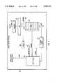
- FIG. 12is a schematic block diagram showing the connection of a processor to hub circuitry in an asynchronous fashion
- FIGS. 13A and 13Bare block diagrams depicting the format for a control word and data word according to an embodiment of the present invention.
- FIG. 14is a block diagram showing synchronous internal logic for accommodating asynchronous external signals according to an embodiment of the present invention.
- FIG. 15is a timing diagram showing write timing with dual register/address banks
- FIG. 16is a schematic block diagram showing details of components of FIG. 14;
- FIG. 17is a timing signal showing write timing according to previous devices without a dual register/address bank
- FIG. 18is a block diagram of an asynchronous update state machine.
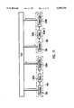
- a data communication system for isochronous datacan be configured in a star-topology with a plurality of nodes 42a, 42b, 42c, each coupled to a hub 44a by data links comprising physical data transmission media such as one-way twisted pair wires 46a-46f.
- the number of nodescan be adjusted depending on the data transmission needs and objectives of the system.
- each hubis configured to accommodate connection with up to 16 nodes.
- Each node 42a, 42b, 42cincludes circuitry 50a, 50b, 50c for receiving data, converting it to a form suitable for transmission onto the physical media 46a, 46c, 46e using transmitters 78a, 78b, 78c and receipt of signals from the physical media 46b, 46d, 46f using receivers 79a, 79b, 79c and conversion to a form suitable for use by the data sinks.
- Each of the nodes 42a, 42b, 42cincludes data sources and sinks 48a-48g.
- the data sources and sinkscan be isochronous sources and sinks such as video cameras 48a, 48d and monitors 48b, 48e, non-isochronous sources and sinks such as an Ethernet media access controller 48c, 48g, and signaling or D channel sources and sinks such as an emulated or virtual key pad 48f provided, for example, on a personal computer (PC) terminal.
- isochronous sources and sinkssuch as video cameras 48a, 48d and monitors 48b, 48e
- non-isochronous sources and sinkssuch as an Ethernet media access controller 48c, 48g
- signaling or D channel sources and sinkssuch as an emulated or virtual key pad 48f provided, for example, on a personal computer (PC) terminal.
- PCpersonal computer
- Each of the nodes 42a, 42b, 42ccan include various types of sources and sinks such as strictly isochronous sources and sinks, such as depicted for node one 42a, strictly non-isochronous sources/sinks as depicted for node three 42c or both isochronous and non-isochronous sources and sinks as depicted for node two 42b.
- the networkis able to operate properly even when connected to one or more nodes which are incapable of communicating using the time-division-multiplexed frame structure described below.
- the hub 44acould be connected to one or more nodes which contain only previously-available circuitry such as 10 Base T.
- the hubis able to detect whether a particular node is capable of time-division-multiplexed frame structure communication as described below. If the node does not have this capability, the hub will fall back to, e.g., a 10 Base T compliant communication mode.
- a networkcan operate in a mixed environment, having some nodes which operate using the time-division-multiplexed frame structure described below and other nodes which operate according to previous protocols.
- This system of automatic detection and fall back to a compliant communication modeis described in greater detail in commonly-assigned application Ser. No. 07/971,018 (Attorney Docket No. 8332-319/NS-2026), titled “NETWORK LINK ENDPOINT CAPABILITY DETECTION” filed on Nov. 2, 1992, and incorporated herein by reference.
- the physical layer of the networkis the circuitry between the media access controllers and the media (in the nodes) and between the repeater circuitry (if any) and the media (in any hubs).
- the physical layer 52 of the network system depicted in FIG. 2has portions which include the physical media 46a-46f and physical layer devices such as the node data receivers and converters 50a, 50b, 50c and the hub components 54a, 54b, and 54c.
- the physical layercan include devices for providing, e.g., transceivers for 10 Base T cables, data multiplexing, phase locked loop circuitry, FIFOs or other circuitry for cable length adjustment, smoothing, squelch and the like.
- the hub 44aincludes circuitry 54a, 54b, 54c for receiving data from the physical media 46a, 46c, 46e separating the isochronous-sourced data from the non-isochronous-sourced data and the D channel and M channel data and converting separated data into a form suitable for handling by downstream hub circuitry 56.
- the separated isochronous-sourced datais provided to a time slot interchange controller 58 for placing the data on a high-bandwidth bus so that it can be transported to destination nodes, e.g., on other TSI controllers in the same hub or in other hubs (as depicted in FIGS.
- non-isochronous-sourced dataincludes Ethernet data
- the hub circuitry 60can be a standard Ethernet repeater processor. In this way, the network can be at least partially backwards-compatible with previous Ethernet hub systems.
- the D channel and M channel informationis provided to a processor 62 which performs various maintenance and control functions such as identifying and alerting users of error conditions, and setting up requested connections, i.e. source/destination paths e.g. by communicating with the isochronous and non-isochronous controllers 58, 60, e.g. over data path 64.
- the isochronous controller 58can be a data exchanger, e.g., an isochronous switching device, such as that described in commonly-assigned application Ser. No. 08/146,337 (attorney docket no.
- the non-isochronous controller 60can be, e.g., an Ethernet repeater.
- a number of star-topology systemscan be interconnected e.g., by connecting hubs 44a, 44b, 44c to one another in a ring structure as depicted in FIG. 3A wherein each of these hubs have nodes attached in a star topology or by connecting hubs 44d, 44e, 44f in a tree structure as depicted in FIG. 3B wherein 44d has 44e and 44f connected to it in the star topology.
- FIG. 3AA number of star-topology systems can be interconnected e.g., by connecting hubs 44a, 44b, 44c to one another in a ring structure as depicted in FIG. 3A wherein each of these hubs have nodes attached in a star topology or by connecting hubs 44d, 44e, 44f in a tree structure as depicted in FIG. 3B wherein 44d has 44e and 44f connected to it in the star topology.
- the hubs 44a, 44b, and 44care connected in a ring-topology with first hub 44a sending data to the second hub 44b, the second hub 44b sending data to the third hub 44c, the third hub sending data back to the first hub 44a via a ring latency adjustment and cycle generator circuitry.
- the datais sent in the same form as output onto the high bandwidth hub bus by the time slot interchange controller 58 and thus the inter-hub connections are referred to as a Time Slot Interchange (TSI) ring.
- TSITime Slot Interchange
- an FDDI-II systemcan be used as a backbone to carry the TSI ring data to other hubs as illustrated by 58f in FIG. 3A.
- Data sent from isochronous device 48dis a continuous stream of digitized data from e.g. a video camera.
- the data from isochronous device 48dwill be taken as having a data rate equal to the American "T1" standard of 1.544 Mbps.
- Data output from the Ethernet MAC 48cis provided at the standard 10 Base T Ethernet rate of 10 Mb/sec.
- D channel informationis provided from a D channel data stream source, preferably contained in a MAC or other circuitry in the system, or, for example, from the virtual key pad 48f at a variable data rate, such as a rate not exceeding about 64 Kbps.
- These incoming data streamsare provided over lines 66a, 66b, 66c to node circuitry 50b' (FIG.
- the incoming data from the various sourcesis provided to a multiplexer 70 which performs time-division multiplexing on a four-bit basis.
- the pattern for the time-division multiplexingis a repeating series of frames or templates. In this embodiment, the frames are repeated every 125 microseconds.
- Table IAdepicts the manner in which the various data streams, and additional data and control bytes are time-division multiplexed.
- Each symbol in Table IArepresents four bits of data so that every group of two symbols represents one 8-bit byte of data.
- Erepresents four bits of data from the non-isochronous Ethernet stream 66a
- Bdesignates four bits of data from the isochronous stream 66b
- Drepresents four bits of data from the signaling or D channel stream 66c
- Mrepresents four bits of M channel data which 66d preferably is provided by circuitry 50b.
- certain byte-length patternsare provided.
- JKrepresents a frame synchronization pattern
- EMthe first two bytes of block three in Table IA
- EMrepresents an Ethernet "pad” followed by a maintenance nibble as described below.
- each framecontains 256 bytes which can be considered in thirty-two groups of eight bytes each, or four blocks of sixty-four bytes each.
- the frame structureis described more thoroughly in commonly-assigned application Ser. No. 07/969,911, (Attorney File No. 8332-315/NS-2024), titled “NETWORK FOR TRANSMITTING ISOCHRONOUS-SOURCE DATA WITH A FRAME STRUCTURE” filed on Nov. 2, 1992, and incorporated herein by reference.
- Table IBAnother frame format that can be used in connection with the present invention is shown in Table IB.
- the frame template of Table IBshows a frame for all-isochronous communication (as opposed to mixed isochronous-Ethernet communication of Table IA).
- Table IBis similar to Table IA, with replacement of all "E” symbols with "B” symbols.
- the last one or two bytes in each blockare "Idle" data bytes.
- the data sent over the physical media 46ais received in the hub 44a.
- the hubcontains a plurality of circuit devices 54a, 54b, 54c, each one coupled to one of the nodes 42a, 42b, 42c by the physical layer/physical layer interface.
- the data transmitted over the physical layer/physical layer interfacearrives serially at a deserializer/decoder 80.
- Link detect circuitry 82also receives the data from the physical layer/physical layer interface for detection of the mode in which the node is operating (e.g. 10 Base T, isochronous-Ethernet or isochronous) and outputting a mode select signal, as described more fully in commonly-assigned application Ser. No. 07/971,018, (Attorney File No.
- the deserializer/decoder 80receives a reference clock signal 84.
- the de-serializer/decoderincludes circuitry which is functionally an inverse of the multiplexing/encoding circuitry described above. Referring to FIG.
- the deserializer/decoderincludes phase lock decode circuitry 86, the results of which are provided to NRZI decode circuitry 88 which, in turn, provides the decode results to four/five decode circuitry 90, in turn providing results to a de-multiplexer 92 which separates the received data into the isochronous-sourced data 94a the non-isochronous-sourced data 94b and signaling data, such as D channel 94c and M channel data 94d.
- the deserializer/decoder 80also outputs a synchronization signal, derived from the JK frame synchronization symbols 96 for use by a framing timing generator 98.
- Both the non-isochronous-sourced data 104 (FIG. 5) and the isochronous-sourced data 102are made available to the hub circuitry 56 or components 54a, 54b, 54c (FIG. 2), as needed for transmission back to destination nodes.
- the separated isochronous data 102 and non-isochronous data 104are reconfigured by the respective interfaces 58, 60 to provide isochronous output 102 and non-isochronous output 104 in a form suitable for processing so as to provide the data as needed for transmission to the destination nodes via the physical layer.
- the non-isochronous data 94bis configured by the physical layer E interface 59z (FIG.
- the output data 104can be processed by a repeater device for eventual transmission to destination nodes.
- packet connectionsmay be linked through media access control layer bridges.
- the output data 104is in a form such that it can be handled by repeater circuitry of types previously available.
- the output data 104is in a form such that it can be handled by a standard Ethernet hub repeater 60 such as Model DP83950 "Repeater Interface Controller” (RIC) available from National Semiconductor Corporation, Santa Clara, Calif.
- This configurationprovides the advantage that the described network can be implemented without the necessity to replace all hub circuitry, in particular without the necessity for replacing hub repeater circuitry.
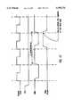
- FIG. 6depicts one implementation of an E interface 59z of a type which will receive the non-isochronous data 94b and provide outputs 104a, 104b of a type that can be processed by previously-available repeater circuitry 60z.
- the non-isochronous datais received in a first-in-first-out (FIFO) buffer 112 to smooth out data rates.
- Circuitry 114detects "no carrier" symbols, provided to emulate Ethernet data packets, which will be used by logic circuitry or state machine 116 to output carrier detect signals.
- the output 118 from the FIFO 112is provided to a multiplexer 120 and a de-serializer 122 to produce data output 104a.
- the multiplexer 120can receive a preamble stream 124 to provide the proper preamble bits in the output data 104a.
- Output 118 from the FIFO 112is also provided to decode circuitry 128 to recognize alignment error symbols and output appropriate signals 132 to state machine 116. Operation and components of the receive interface 59 are described more thoroughly in application Ser. No. 07/970,329, (Attorney File No. 8332-316/NS-2022), filed on Nov. 2, 1992 U.S. Pat. No. 5,361,261.
- data from isochronous-source 48dis transmitted in the first 24 bytes of each frame represented by the "B" symbols in block 0 of Table IA (i.e. the first forty-eight "B" symbols in the frame structure).
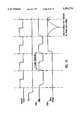
- FIG. 7is a schematic diagram of a hub signalling processor in a hub and its connections for receiving and buffering data onto a high bandwidth bus.
- the separated isochronous data 102is stored in one of two buffers 132a, 132b.
- the timing of storage in the buffers 132a, 132bis coordinated with the 125 microsecond frame transmission timing so that data 102 from a first frame will be stored in the first buffer 132a during a first period of 125 microseconds and, during the next 125 microsecond period, the isochronous data 102 from the next frame will be stored in the second buffer 132b.
- the datacan be stored in the buffer 132 in the same order it is received, such that the eight bits represented by the first two "B" symbols in Table IA is stored in the first storage location of buffer 132a, that corresponding to the second two "B” symbols in Table IA is stored in the second location of buffer 132a and so on. Since the frame structure depicted in Table IA contains 96 bytes of isochronous data per frame, each of the buffers 132a, 132b has the capacity to store 96 bytes of data per node supported.
- Bus 134has sufficient bandwidth to carry the isochronous data output from a plurality of nodes which are connected to the hub 44a. In an embodiment in which the hub 44a is connected to 16 nodes, the bandwidth of the bus 134 must be sufficient to receive 1,536 bytes of data (i.e. 16 nodes ⁇ 96 bytes per node) every 125 microseconds (i.e. every frame). This corresponds to a bandwidth of about 98304 Kb/sec.
- the 98304 Kb/sec bandwidthis particularly useful because it substantially matches the bandwidth employed in FDDI-II, making it particularly easy to port the data on the TSI bus 134 to a TSI ring 58f (FIG. 3A) in configurations where the TSI ring 58f is an FDDI-II system.
- the datais conveyed from the buffer 132 onto the bus 134 in a time slot interchange fashion, and thus the bus 134 is referred to as a time slot interchange (TSI) bus.
- TTItime slot interchange
- each 125 microsecond time periodis divided into 512 equal time slots, each one of which is used to convey five bits of information (on average, conveying 4 bits of data and one timing bit).
- each 125 microsecond time frame on the physical layer/physical layer interfacecontains 512 time slots, each of which has a duration of about 0.2441 microseconds.
- the data carried on the TSI bus 134is transmitted in 125 microsecond time frames divided into 1,536 time slots, each of which has a duration of about 0.08138 microseconds.
- connection switch table 140contains two sets of 1537 locations, one for each one-way direction.
- the 1537 locations in the connection switch tablecontain bits to be used for control of the switching of the B slots either to another node or to the TSI bus.
- the 24 bytes of data per 125 microsecond framewere conveyed in the first 24 B slots of the frame transmitted from 48d.
- the data from the source 48dwill be stored in the isochronous data buffer 132.
- the destination of the datais 48b.
- the 24 B slots of datawill be transferred to data buffer 154a and then transmitted to 48b in its corresponding first 24 B slots.
- the 24 B slotscould have been destined for the TSI bus in which case the 24 B slots in 132 would have been switched onto the TSI bus.
- a bit of the contents of the switch tablewould have controlled line 150 to control the multiplexer. Assuming the first 10 time slots of the TSI bus do not receive the B data which is destined for a node attached to the isochronous switching device during the first TSI time slot, the multiplexer control 150 will be "0" and no data will be output from the buffer 132 onto bus 134. The multiplexer 146 will merely convey along the TSI bus 134 whatever data was already on the TSI bus in the first time slot.
- the control signal for multiplexer 146will be "1" and a byte of data stored in the appropriate data location of buffer 132 will be output through multiplexer 146 onto the bus 134.
- Which data location of the buffer 132 is "appropriate”is determined by the D channel or call setup and can be indicated by a read pointer (e.g., contained in the switch table).
- buffer 132is a random access memory (RAM) and the read pointer will be determined according to the contents of the switch table location representing the TSI slot frame.
- RAMrandom access memory
- the read pointerwill be determined according to the contents of the switch table location representing the TSI slot frame.
- FIG. 7also depicts how the isochronous data is retrieved from the TSI bus 134 for transmission to a destination node.
- Isochronous switching device circuitry 58is provided for support of the node connections.
- the data from the TSI ringis processed by circuitry 58 which is associated with node 1, i.e., the node with contains data sink 48b. Data carried on the TSI bus will be loaded into one of the buffers 154a, 154b.
- the two buffers 154a, 154bare controlled to provide timing similar to the timing of the buffers 132a, 132b described above. That is, during a first time frame, the first buffer 154a will be receiving data from the TSI ring while the second buffer 154b is outputting data (which was stored during the previous time frame) to physical layer circuitry 54a for transmission onto the physical media to the destination node 42a. During the next time frame, the roles of these buffers will be reversed such that data retrieved from the ring will be stored in buffer 154b and the data stored in 154a during the previous frame will be output for ultimate transmission to the destination node 42a.
- Retrieval from the TSI ringis achieved by a multiplexer 156 controlled by a control signal 158 output over line 160 from the processor 138, relying on a connection switch table 162 in a fashion similar to that described for control of multiplexer 146.
- Control datais stored in an output table 162 according to destination information provided over the D channel to the processor 138.
- the TSI bus datais loaded into the buffer 154.
- data from the TSI ring 134may or may not be stored in the buffer 154a (depending e.g., on the absence or presence of a local loopback procedure for this data).
- the control signal output from the processorcauses data from the TSI bus 134 to be stored into the buffer 154a.
- datamay or may not be provided from the TSI bus 134 to the buffer 154a.
- time slots 11 through 35 from the TSI ringare stored in the buffer 154a.
- the data from the buffer 154ais output over line 164 for transmission to one or more destination nodes attached to hub 44a and specifically node 42a, in this example.
- datais output from the buffer 132a onto the TSI bus 134 in the same order it was received, this is not necessarily the case.
- the processor 138provides addresses via pointer 1210, (FIG. 12) to the buffers 132a, 132b to determine the order in which data stored in the buffers 132a, 132b is provided to the TSI ring 134.
- Pointer 1212is used to indicate addresses for the buffers 154a, 154b, to determine the order in which data from the TSI ring 134 is stored into the buffers 154a, 154b.
- addresses output from the processor 138to control the locations in which data retrieved from the TSI bus 134 is provided to the attached nodes.
- the receive table and transmit table 140, 162are depicted as part of or directly writable by the processor 138. This type of configuration, however, can lead to inefficiencies. In particular, in the embodiment of FIG. 7, the processor cannot write into the tables 140, 162 during periods when the tables 140, 162 are being used for switching data.
- FIG. 12depicts another configuration which permits the processor 138a to update the receive and transmit switch tables 140, 162 without such inefficiency.
- the processor 138ais preferably used to control a variety of operations in the isochronous system. Operations which the processor handles include the call control or signaling, maintenance activities at the isochronous physical layer and system level connections and/or TSI ring, switch table updating, status/control bit processing and error bookkeeping.
- the processor interfaceis also responsible for passing on error conditions which occur on the TSI ring A, TSI ring B, or port interface.
- the procedure for updating the receive table 140will be described first.
- the processorwrites data and addresses (preferably, in a format to be described below) in a "burst" to a single register address 1202.
- the size of the data output in a burstis preferably selected so that all of the data from the burst can be loaded into the switch tables during a minimal number of TSI frames, preferably during a single TSI frame.
- the window during which the switch tables are not being accessedis about 116 nanoseconds. In this embodiment, it is possible to do between about 15 and about 19 updates in a window of 116 nanoseconds. Accordingly, in one embodiment, the size of the transfer burst from the processor is about 16 words.
- the processorcan write up to 16 words of data into the register 1202 over data bus 1214 and address bus 1216.
- the 16 words from the register 1202are stored into a set of 16 "shadow" registers known as a "receive holding register” 1204. Providing a shadow register simplifies the procedure from the point of view of the processor since the processor can do a write of all 16 words to a single address, rather than 16 separate addresses.
- the updates to the receive switch table 140are written from the receive holding register 1204 during the appropriate times during the frame of data being passed through the switch. Preferably, parity is generated for the switch table data location after it is unloaded from the holding register to assure data integrity.
- Timing of the transfer into the receive switch table 140is controlled by a control circuitry 1206 which receives timing information from the port interface or the TSI ring "B" window 1208. Based on the timing information, the control circuitry 1206 determines the beginning of a first time period during which the switch tables are not in use and initiates writing of the data from the holding registers 1204, 1224 into the switching tables 140, 162, respectively.
- a similar structureis provided for updating the transmit table 162, including a register such as a 16 word register 1222, a transmit holding "shadow” register, having a set of 16 one-word registers 1224, control circuitry 1226, receiving timing information from a TSI ring "A" window 1228.
- FIG. 12depicts registers 1202 and 1222 as separate registers, if desired, a single register can be used for the function of registers 1202 and 1222.
- the switch table and the processorare asynchronous in the sense that they run in accordance with two different clocks.
- the processorruns at a 33 MHz clock while the switch table runs at a 12.5 MHz clock.
- the registers 1202, 1204, 1222, 1224can write to either side of the asynchronous boundary 1252, it is necessary to assure that two sequential writes according to different clocks are still able to provide data into the proper registers.
- the low pulseis sampled and the sampled signal is provided to a one shot which enables the controller 1206, 1226 to determine when the rising edge of the clock occurs.
- This schemeavoids the need for an asynchronous reset.
- a delayis instituted. In the absence of such a delay, if there is a write according to the 12.5 MHz clock, followed by a write according to the 33 MHz clock, the write before the 12.5 MHz clock will extend into the 33 MHz time. The delay pushes that time back until the actual time of the write.
- two types of wordsare sent to the registers 1202, 1222 and the holding registers 1204, 1224.
- a single holding register system for both received and transmitcould be used, separate holding registers for the receive and transmit switch table updates provides for efficient updating of the appropriate switch table such that the updates of one switch table are independent of the other.
- An example in which this scheme is more efficientis where asymmetric calls or half-duplex calls are established. Selection of the appropriate switch table holding register is done through the switch table holding register data window and is done by the processor addressing the appropriate holding register.
- the words sent to the registersare control words and data words.
- the control wordis used to indicate the switch table and the switch table address so that when the data words are loaded into the receive and transmit tables, it is known in which table (if more than one) and at what location in the tables these words should be stored.
- the data wordcontains all the data to be loaded into the switch table data location.
- the control word and data wordalso contain additional information.
- FIGS. 13A and 13Bdepict the structure of a control word and a data word according to one embodiment. Table IV indicates the meaning of the bit indications in FIGS. 13A and 13B.
- the receive switch tablerequires the switch table location address (corresponding to a time slot in a TSI ring), the receive buffer address (corresponding to a port B channel or TSI ring B time slot), external transmit enable (ETE) bit, internal transmit enable (ITE) bit, and a tri-state enable (TSE) bit.
- the transmit switch tablerequires the switch table location addressing (corresponding to a port B channel or TSI B time slot), the transmit buffer address (corresponding to a TSI ring A time slot), external transmit enable or idle address bit (depending on the embodiment) (ETE/IA bit), idle pattern enable (IPE) bit, and TSE bit.
- IMCIsochronous maintenance channel which is part of the TSI cycle header and "idle address” refers to external transmit enable/or idle address (depending on the embodiment).
- the data and control words output by the signaling processorare provided according to operating software of the processor.
- the operating softwarecan obtain information regarding the network addresses of each of the end points (nodes) and the bandwidth allocated to each. It can handle channel allocation on this basis. Based on the network connection table, all connections within the local system are established, released, and monitored by the processor 138a.
- a single switch table slot updaterequires one control word and one data word.
- the control/data C/D bit 1302a, 1302bindicates whether the word is a control word or a data word. This bit is also used in conjunction with permitting multiple data words to be associated with a single control word.
- a switch table updatemay contain multiple words where the first word is the control word and the remaining words are data words, as indicated by the control/data C/D bit.
- the control word switch table address 1304ais used as the base address for the first data word (i.e., the data word following the control word).
- the switch table addressis incremented by a specific count and (if more than one data word follows the control word) the next data word is loaded into the location of the switch table indicated by the incremented address.
- the amount by which the address is incrementedis preferably programmable, for example, by setting a bit in a register 1242 under control of the processor.
- the increment countis selectable to be either 1 or 16, with the default count preferably being 16. Providing for a programmable count is useful in different types of switching. By incrementing the address by one, the switching of data on the TSI ring in consecutive slots can be set up.
- the preferable count of 16is directly associated with mapping of consecutive data in TSI slots to a single isochronous/Ethernet (isoEnet) node or vice versa.
- By incrementing the address by 16the switching on consecutive slots corresponding to a particular node can be set up.
- incrementing the switch table for that ring by 1allows consecutive slot switching.
- incrementing the switch table address by 16maps the data to the port locations in the switch table.
- the C/D bit for updating multiple wordsif a switch table update is to contain six consecutive switch table entries, seven 16-bit words for the switch table update are required in the depicted embodiment.
- the first 16-bit wordcontain the starting switch table location (indicated by the control bit C/D 1302a being set to 1).
- the next 16-bit wordcontains the data information.
- the remaining five data words, for a total of six switch table updatesrepresents one slot of the switch table. In this example, these are to be stored in consecutive slots, and the offset from the first switch table location is incremented by one each time data information is read from the holding register. If, for example, the switch location started at location 1000, the first switch table data would be loaded into location 1000 and the final switch table data into location 1005.
- the end of the consecutive datais indicated when the control bit 1302a is set indicating a new switch table update sequence (or the LD bit 1306 is set, indicating the last data word in the switch table update burst, as described below).
- the processorcan assert the last data (LD) bit 1306 in the last word it writes to the switch device.
- LDlast data
- the processor 138ait is preferred to relieve the processor 132a of this burden so that the processor will be free to perform other tasks during the transfer into the switching tables 140, 162.
- the LD bitis used to provide to the local circuitry an indication of the end of the switch table update providing further efficiency.
- the processor 138ais configured to increase or maximize efficiency of update data transfer, e.g., by delaying such transfers until a full or nearly full register (i.e., 16 words) can be transferred.
- a full or nearly full registeri.e., 16 words
- one update of 16 wordsis more efficient than eight updates of two words each.
- the update processshould be undertaken regardless of sub-maximal system efficiency.
- the switch tables 140, 162are in use the majority of the time, i.e., during a majority of a TSI cycle. According to the present embodiment, it is not necessary for the processor 138a to wait until the non-use portion of the TSI cycle before outputting the data for updating the switch tables.
- the updatescan be written by the processor whenever the processor has new data to be written into the switch tables and no current updates are taking place, despite the fact that the actual time the updates can be performed is limited to a small amount of time during the TSI frame.
- the processorAfter the processor has loaded data words and control words into registers 1222, 1202 and these data have been loaded into the holding registers 1224, 1204, the data will be held in the registers 1224, 1204 until such time as the switch tables 140, 162 are not in use.
- the control circuits 1206, 1226will initiate writing of the data in the data words stored in the holding registers 1204, 1224 into the respective switching tables 140, 162.
- the data wordswill be read out in the order they were written in. If a word in the holding table is a control word, the new switch table address contained in the control word is stored for use in writing the subsequent data into the switch tables 140, 162.
- the processoris preferably interrupted to indicate that it can send more switch table update information to the switch device.
- the processor 138aafter outputting a burst of data and control words, will typically be prevented from attempting another output of control and data words until completion of the transfer of the previously output words into the switch tables.
- an LD bitis output into the registers 1222, 1202, 1224, 1204 (or the maximum number of words, such as 16 words, have been output)
- the processorwill output control and data words to the registers 1202, 1222 only in response to an interrupt.
- an "empty" bit in a register 1242will be set to "0" to indicate that the switch table update process should not be interrupted until it has completed whereupon the bit is set to "1" indicating that the holding register is empty.
- This bit of the register 1242will be set to "1" once the updating of the switch table 140, 162 has been completed.
- control of the timinginvolves a state machine.
- the state machineis in an idle state 1802 (FIG. 18) in which there are no new updates and the processor is not performing any writes to the register.
- the processorbegins writing 1804 to a register, the machine enters the write state 1806.
- the machinewill remain in the write state until the writing is finished 1808 (either indicated by setting the LD bit or upon sending 16 full data and control words). Updates are prevented from being initiated until there is a successful exit from the write state. This is to prevent a situation in which the processor stores some of the words for an update but does not complete the update burst.
- the state machineenters the update state 1810. During the update state, the processor is prevented from writing more data into the registers since this could overwrite some of the data which was to be stored into the switching tables. After the switching tables have been updated 1812 according to the information in the holding registers, the state machine will return to the idle state 1802 and an interrupt will indicate to the processor 138a that additional updates can be sent to the registers 1202, 1222, if desired.
- Isochronous switching circuitry 58can also be provided with a local loopback capability.
- the local loopback capabilitypermits circuitry 58 to transfer data directly from the receive buffer 132 to the transmit buffer 154 without first placing the data onto the TSI ring 134, thus freeing TSI bus bandwidth. This is the case, e.g., when data from a source attached to hub 44a is destined to another node attached to hub 44a.
- Local loopback capabilityis described more thoroughly in commonly-assigned application Ser. No. 07/969,910, abandoned, (Attorney File No. 8332-317/NS-2025,) titled "LOCAL LOOPBACK OF ISOCHRONOUS DATA IN A SWITCHING MECHANISM", filed on Nov.
- Local loopback capabilityis useful, for example, when both an isochronous source and an isochronous sink are connected to the same hub.
- both the video camera isochronous source 48d on node 2 and the video monitor isochronous sink 48b on node 1are connected with the same hub 44a.
- Local loopbackcan be used to provide data to the monitor 48b for displaying images received by the video camera 48d, substantially in "real time,” but without placing the data on the TSI bus 134, thus allowing the bandwidth to be used by other connections.
- non-isochronous data from source 48c on node 2, 42bis intended for the non-isochronous sink 48g on node 3, 42c, and thus the E data is transmitted via 50b across 46c to 54b which demultiplexes the E data and conveys it to 60.
- Circuitry 60conveys the E data to 54c which multiplexes it into the frame and transmits it across 46f to 50c which demultiplexes the data and provides it to 48g.
- the hubAfter the hub has received data from a node and conveyed it to a location for transmission to the destination node or nodes, the data which is intended for the destination node may need to be placed in a form suitable for transmission across the physical media via the physical layer if intended for an attached node.
- data 166 output by an Ethernet repeater 60the data is transformed by an E transmit interface 168 into a form suitable for multiplexing with other data streams, such as an isochronous data stream 66b and D channel and M channel data bits 66c.
- E transmit interface 168An example of an E transmit interface 168 is depicted in FIG. 8.
- the transmit interface depicted in FIG. 8is in general, the functional inverse of the E receive interface 59z depicted in FIG. 6.
- Data 166could be supplied either in serial or parallel form. If in serial form, the data 166 is de-serialized and is then combined with any necessary alignment error bits 172 in a multiplexer 174, the output of which is conveyed to a FIFO 176.
- a sync detect circuit 178extracts synchronization information from the repeater output 166 for conveying to a state machine 180.
- the state machine 180also receives carrier detect information 184, framing counter information 186, and provides control signals 188 to the FIFO 176.
- Datais extracted from the FIFO 176 as needed to make up a frame for transmission over the media 46 as described below.
- the data output from the FIFO 176is multiplexed with preamble bits 190 and "quiet" (null carrier) bits 194 by a multiplexer 196. Operation of the E transmit interface is described more thoroughly in the application Ser. No. 07/970,329, (Attorney File No. 8332-316/NS-2022).
- the data 66a output from the E transmit interface 168is provided along with isochronous data output 66b and maintenance and D channel data 66c to encoder serializer circuitry 202, as depicted in FIG. 9.
- the encoder/serializer 202is configured substantially like the encoding circuitry found in the node and depicted in FIG. 4. Specifically, the encoder/serializer 202 provides a multiplexer for combining the three streams of data 66a, 66c, 66b, a four/five encoder, an NRZI encoder, and pre-emphasis circuitry. The timing of transmission is controlled by transmit timing circuitry 204.
- Output 206 from the encoder/serializeris selectively combined with link beats from a link beat generator 208 by multiplexer 210 for purposes of link end point detection, as described more thoroughly in application Ser. No. 07/971,018, (Attorney File No. 8332-319/NS-2026).
- the data sent from the hub 44a to the nodes 42is sent in a frame format which is preferably substantially the same as the frame format used for the data sent from the nodes 42 to the hub 44a as described above.
- the circuitry 50includes devices (FIG.
- the frame structure of Table IAprovides an allocation of bandwidth such that the data rate for the non-isochronous data are compatible with e.g. 10 Base T Ethernet data rates.
- Another frame structure usable in connection with the present inventionis shown in Table IB.
- Other types of frame structurescould be used in connection with other isochronous and/or non-isochronous data sources and sinks such as token ring non-isochronous sources and sinks, in which case a different frame structure can be used to provide an allocation of bandwidth suited for the particular purpose.
- the time-multiplexed datais then encoded by an encoder 72.
- the encoderperforms four/five encoding.
- the five bit code symbols of the particular four/five implementationhave been chosen so as to maintain the AC balance of the physical medium, and to minimize the frequency spectrum of wave forms as they are transmitted along the physical medium. This eases the task of the data decoder, which is typically a phase lock loop device, in recovering the data and the transmission clock.
- These patternswhen properly combined, have a maximum of three bit times with no transition. With a bit rate of 48.8 ns, the minimum transition rate is 3.41 MHz or 146.5 ns between transitions.
- datais expected to appear in an integral number of 4-bit nibbles. This may not be the case if an Ethernet packet suffers from the addition of "dribble bits" which do not make up an integral number of nibbles. In this case, a code symbol "unaligned data" is transmitted.
- the results of the four/five encodingis then further encoded by encoder 74 using a non-return to zero, inverted (NRZI) scheme.
- the NRZI encodermodifies the bit stream by inverting the output whenever a logic 1 is transmitted. Logic 0 produces no change in state.
- the four/five-NRZI encodingis particularly useful in networks in which a non-isochronous source is a 10 Base T Ethernet source. This is because the four/five-NRZI encoding provides for transmission at a signaling rate such that the data rate for the non-isochronous portion of the data is substantially compatible with the data rates provided and expected by the Ethernet MAC. In typical Ethernet systems, a data rate of 10 Mb/sec is provided.
- the data provided at this rateis encoded using a differential manchester scheme using two transition times to transfer one bit of data. On average, this scheme provides one clock bit per every bit of data.
- the standard Ethernet data rate of 10 Mbit/sec, after manchester encodingresults in a signalling rate of 20 Mbit/sec.
- a frame of datacontains 313 "E" symbols or 1252 E bits.
- the present schemehas a capacity for transmitting 10,016 Mbits/sec of Ethernet-sourced data interspersed with 6144 Kbits/sec of isochronous data.
- the data rate and signaling rateis within two and one-half percent of the signaling and data rate used by 10 Base T, allowing both isochronous traffic and Ethernet traffic to travel over existing physical media without seriously degrading the data rate of the Ethernet traffic, compared to previous standard Ethernet systems.
- provision of substantially standard Ethernet data ratescontributes to the ability to implement the described network without the necessity for replacing in-place MACs or repeater circuitry.
- the ability to convey data frames substantially at the signaling rate used by previously-available systems, such as standard Ethernetcontributes to the ability to implement the described network without the necessity to replace in-place physical media, such as twisted pair media.
- the four/five-NRZI encodingis particularly useful in connection with an Ethernet non-isochronous source
- other types of encoding or decodingcan also be used in the present system, including, e.g., a scheme encoding 8 bits into 10 bits.
- additional types of encoding or decodingcan be provided tailored to the requirements of other non-isochronous sources/sinks, such as token ring non-isochronous sources and sinks.
- the more important aspect of encodingis not as much the particular encoding scheme used as selection of an efficient coding scheme and particularly a scheme having sufficient efficiency that the bandwidths of both the incoming non-isochronous data 66a and the incoming isochronous data 66b can be accommodated on the physical media without seriously degrading bandwidth formerly available for the non-isochronous data.
- the four/five encoding schemeis more efficient than differential manchester encoding scheme, in this regard, since it provides four bits of data for every five potential transitions so, on average, that one clock bit is provided for every four bits of data (as opposed to one clock bit for every data bit in differential manchester encoding).
- the differential manchester coded datatook up substantially the entire bandwidth of the twisted pair media, which has a maximum effective signalling rate of about 20 Mb/sec
- the four/five-NRZI encodingpermits physical media having the same bandwidth to accommodate both the 10 Mbit/sec Ethernet data stream and a 6144 Kbit/sec isochronous stream, as well as a 64 Kbit/sec D channel, a 96 Kbit/sec maintenance channel, and 64 Kb/sec for the frame synchronization pattern.
- the data rate output from the isochronous source 48dis 1,544 Mb/sec.
- the frame structure noted aboveprovides an isochronous bandwidth capability of 6,144 Mb/sec.
- the single isochronous source 48b in the present examplecan be entirely accommodated using only 48 of the 192 "B" symbols per frame (i.e. 24 bytes per frame or 192 bits per frame). This leaves 72 "B" symbols per frame unutilized by source 48d.
- a basic rate ISDN Channelcould be supported by using three 64 Kb/s slots within the isochronous channel. It would also be possible to transmit data from up to ninety-six isochronous sources, each outputting data at a rate of 64 Kb/s.
- the networkit is possible to use the network to transfer data from a single isochronous source outputting at a rate of 6.144 Mb/s or the isochronous bandwidth available may be allocated with a granularity of 64 Kb/s, i.e. it may be split into multiples of 64 Kb/s.
- the output from the NRZI encoding devicesis sent to pre-emphasis circuitry 76.
- the pre-emphasis circuitrycompensates the signal transmitted onto the physical medium to reduce the jitter.
- the pre-emphasis stageis optimized for the frequency spectrum employed by the present system.
- the data output by the pre-emphasis circuitry 76is sent to a transmitter or driver and the signal is transmitted over the physical medium 46c.
- the physical medium 46ccan be any of a number of media types including twisted pair, coaxial or fiber optic cable.
- the networkis configured so that the desired data rates can be achieved within the bandwidth inherent in twisted pair media and it is anticipated that at least initial use of the disclosed embodiments will make frequent use of twisted pair as media in order to take advantage of twisted pair networks already in-place.
- certain features of the networkare preferably configured to accommodate the characteristics (including the delay characteristics) of twisted pair wiring having a maximum length of approximately one hundred meters.
- FIG. 10depicts a scheme for achieving this type of timing.
- the timingcan be synchronized with a 125 microsecond reference clock signal 214.
- the reference signal 214provides an ascending clock edge every 125 microseconds.
- the reference signalcan be provided by any of a number of sources.
- an embodimentis configured to permit a reference signal 214 to be synchronized to an external clock reference, such as a reference signal from a wide area network or from a FDDI-II ring.
- the reference signalcan be supplied through one of the nodes and transmitted to the hub for distribution to the other nodes, or can be supplied directly to the hub for distribution.
- one of the telephone connectionscan be chosen as the LAN reference. Connection can be made to the other WAN interfaces via data storage and buffers.
- the bufferswould contain multiple frames of data to accommodate the phase and frequency skews between the frame structures apparent upon these connections and the chosen reference.
- the frame structure derived from the wide area network connectionis subject to frequency jitter.
- the present networkis able to accommodate this jitter provided that it is within specified bounds, and accordingly the jitter accommodation will not degrade the integrity of the isochronous channels.
- Each node and the hub devicewill contain its own high-accuracy transmission encoding clock, typically a crystal oscillator.
- the links 46are asynchronous to each other, being referenced only to the sourcing clock oscillator.
- the synchronous frame structureis conveyed over asynchronous links.
- a scheme for synchronizationbecomes necessary.
- One problem associated with synchronous designis interfacing to the real world which is asynchronous by nature.
- a common example of thisis a typical CPU interface.
- One example of a set of CPU signalsis as follows: Data Bus (D[15:0]), Register Address (RA[3:0]), Chip Select (CSz), Slave Write (SWRz), and Slave Read (SRDz). Due to the fact that the control signals (CSz, SWRz, SRDz) are asynchronous with respect to the system clock of an integrated circuit, all input signals must be properly synchronized to the internal clock.
- This synchronization processtakes a maximum of two clock cycles to occur (FIG. 17).
- the purpose of the synchronizationis to eliminate the possibility of metastability on any internal flip-flops.
- One embodimentuses a method for writing data into a synchronous design and still achieves a throughput of one data write per internal clock cycle. It should be noted that this method is not limited to a CPU being interfaced to registers. It could be used in any application in which external signals, which are asynchronous, need to be interfaced to a synchronous logic design.
- the interface logic between the synchronous internal logic and the asynchronous control signalsconsists of a mixed synchronous-asynchronous design.
- a disadvantage in using this interfacing techniqueis that a small portion of the logic must be asynchronous. This disadvantage is believed to be outweighed by the gains of using this technique.
- One advantageis the throughput of one data write per clock cycle throughput.
- FIG. 14There are five main blocks which are involved. These blocks are shown in FIG. 14. The five blocks are: Register/Address Bank 0 1402, Register/Address Bank 1 1404, Synchronizer 0 1406, Synchronizer 1 1408, and Control Logic 1410. Register/Address Bank 0 and Register/Address Bank 1 are identical blocks of logic as are Synchronizer 0 and Synchronizer 1.
- FIG. 16shows a more detailed block diagram of one embodiment.
- the processorwrites to a register by asserting the SWRz control signal.
- the address and datawill be stored in Register/Address Bank 0.
- a synchronization processstarts to take place in Synchronizer 0. While this synchronization is taking place another processor write can occur at one clock period after the previous write.
- the address and data from this writewill be stored in Register/Address Bank 1.
- a synchronization processstarts to take place in Synchronizer 1.
- the first synchronizationwill have finished and SWRz 1502 will assert the write signal (write state 1504 (FIG. 15). When this signal is sampled high synchronously by the internal logic, the data which is in Register/Address Bank 0 will be written into the internal logic.
- the next writemay occur as soon as one clock period from the previous one. This time, the address and data will be stored back into Register/Address Bank 0 and synchronizer 0 starts. Again, during this synchronization process, the data that is in Register/Address Bank 1 is written to the internal logic. This process can then repeat at a rate of one CPU write per internal clock cycle. There are no restrictions on when the writes can occur as long as they are separated by at least one internal clock period.
- the synchronizer 1406includes three flip-flops 1602, 1604, 1606.
- the first flip-flop 1602is set asynchronously.
- Flip-flop 1604is synchronous and runs off the internal clock (ISOCLK). This is the clock on which the registers are running.
- the second flip-flopis used to sample the output of the first asynchronous flip-flop 1602.
- the third flip-flop 1606is provided. This flip-flop is also synchronous with ISOCLK. It is used to sample the output of the second flip-flop 1604. Once the output of the third flip-flop 1606 goes high, it can be used to reset the first asynchronous flip-flop 1602 since it is known not to be metastable.
- the hub 44will begin to transmit a frame to the node, as indicated by the timing marks on time line 216. Because of the line delays in the physical media, the time at which the nodes will receive the frame transmitted by the hub will lag the time when they were sent out from the hub as shown by time line 218.
- a delay 220is introduced in the timing scheme before the node begins transmission of the next frame up to the hub 222.
- the delay 220has a value such that, taking into account the latency introduced by transmission over physical layer/physical layer interface, the hub will begin receiving the transmitted from at times 224 approximately coinciding with the rising edges of the clock signals 214.
- the delaymay be introduced by inserting delay circuitry 226a, 226b between the receiving circuitry 78a, 78b of the nodes 42a, 42b and the transmitting circuitry 226a, 226b of the nodes 42a, 42b. Because the latency of physical media will vary from node to node, typically depending on the length of the links, the length of the delay 226a which is appropriate for a given node may be different from the delay 226b which is appropriate for another node. Accordingly, it is possible to detect the latency or delay of a particular link and use this latency to calculate an optimal delay. The calculated optimal delay can then be programmed into the delay circuitry 228a, 228b as appropriate.
- the disclosed configurationallows the processor to send the data needed to update the switch table as soon as it has new updates to perform, regardless of whether the data can actually be written into the switch table at this time. This frees the processor to perform other tasks without having to wait for an appropriate time during the frame.
- the present inventionprovides a channel for isochronous data such that the bandwidth for a particular isochronous source does not necessarily decrease as isochronous traffic on the system increases.
- the isochronous data transferis interoperable with the transfer of non-isochronous data in a fashion that is transparent to the media access controllers and to the application software.
- the described networkprovides for inter-operating isochronous and non-isochronous data transfer while maintaining the data transfer rate achieved for non-isochronous data in previously in-place systems.
- the described networkcan convey both the non-isochronous data and the isochronous data over in-place physical media without degrading the non-isochronous data transfer rate compared to the rate previously carried by the same physical media.
- Isochronous datais conveyed with a minimized or reduced amount of delay and jitter and with minimized or reduced requirements for buffer memory.
- Bandwidth to be used for a particular isochronous sourceis selectable with a specified granularity, such as 64 Kbits/sec granularity, so that isochronous sources and sinks have available to them an amount of bandwidth which is both selectable and sustainable.
- the disclosed systemprovides a data exchange mechanism which is compatible with standard media access controller devices. Thus, currently available hardware and associated software may be used over the physical links. Incremental upgrade of equipment can be made as desired.
- the hubcan perform call set-up, channel allocation and isochronous channel management, preferably using source/destination information provided over the D channel.
- a number of modifications and variations of the inventioncan also be used. It is possible to use some aspects without using other aspects. For example, it is possible to provide a dedicated bandwidth for isochronous traffic without using a network which receives non-isochronous data from a Ethernet media access controller. It is possible to transmit non-isochronous-sourced data using a continuously-recurring frame structure without providing a plurality of hubs which are inter-connected. At least some aspects of the described network can be implemented in a non-star-topology, such as by communicating isochronous and non-isochronous data which is time-multiplexed into a recurring frame structure, directly between two nodes.
- non-isochronous sources and sinkscan also be used, including token bus, ATM, video phones, video servers, computer work stations or other networking schemes.
- the present inventioncould be used even though no non-isochronous sources are connected to the system.
- the present inventioncan be used even though no isochronous sources or sinks are connected to the system.
- Other frame structurescan be used to provide more or less bandwidth for various types of data such as isochronous data, non-isochronous data, and D channel data. It is possible to operate the described network without using buffers to smooth the "lumpy" data arrival rate, although such an implementation might require replacement of existing MACs. Channels in addition to isochronous, non-isochronous, D channel, and M channels could be provided.
- a 24-port hubincludes 2 Ethernet repeaters, each supporting 12 Ethernet connections, two isochronous switching devices and 24 physical layer portions.
Landscapes
- Engineering & Computer Science (AREA)
- Computer Networks & Wireless Communication (AREA)
- Signal Processing (AREA)
- Small-Scale Networks (AREA)
- Data Exchanges In Wide-Area Networks (AREA)
Abstract
Description
TABLE IA __________________________________________________________________________BLOCK 0: J K E B E B E B E B E B E B E E Group0 E E E B E B E B E B E B E B E E Group1 E E E B E B E B E B E B E B E B Group2 E E E B E B E B E B E B E B E B Group3 E E E B E B E B E B E B E B E E Group4 E E E B E B E B E B E B E B E E Group5 E E E B E B E B E B E B E B E E Group6 E E E B E B E B E B E B E B E E Group7 __________________________________________________________________________BLOCK 1: M M E B E B E B E B E B E B E E Group8 E E E B E B E B E B E B E B E E Group9 E E E B E B E B E B E B E B E E Group10 E E E B E B E B E B E B E B E E Group11 E E E B E B E B E B E B E B E E Group12 E E E B E B E B E B E B E B E E Group13 E E E B E B E B E B E B E B E E Group14 E E E B E B E B E B E B E B E E Group15 __________________________________________________________________________BLOCK 2: D D E B E B E B E B E B E B E E Group16 E E E B E B E B E B E B E B E E Group17 E E E B E B E B E B E B E B E E Group18 E E E B E B E B E B E B E B E E Group19 E E E B E B E B E B E B E B E E Group20 E E E B E B E B E B E B E B E E Group21 E E E B E B E B E B E B E B E E Group22 E E E B E B E B E B E B E B E E Group23 __________________________________________________________________________BLOCK 3: E M E B E B E B E B E B E B E E Group24 E E E B E B E B E B E B E B E E Group25 E E E B E B E B E B E B E B E E Group26 E E E B E B E B E B E B E B E E Group27 E E E B E B E B E B E B E B E E Group28 E E E B E B E B E B E B E B E E Group29 E E E B E B E B E B E B E B E E Group30 E E E B E B E B E B E B E B E E Group31 __________________________________________________________________________ JK = Frame Synchronization Pattern MM = 8 Maintenance Bits D = D Channel EM = Ethernet Pad & 4 Maintenance Bits E = Ethernet Packet Channel B = Isochronous Channel
TABLE IB __________________________________________________________________________BLOCK 0: J K B B B B B B B B B B B B B B Group0 B B B B B B B B B B B B B B B B Group1 B B B B B B B B B B B B B B B B Group2 B B B B B B B B B B B B B B B B Group3 B B B B B B B B B B B B B B B B Group4 B B B B B B B B B B B B B B B B Group5 B B B B B B B B B B B B B B B B Group6 B B B B B B B B B B B B B B I I Group7 __________________________________________________________________________BLOCK 1: M M B B B B B B B B B B B B B B Group8 B B B B B B B B B B B B B B B B Group9 B B B B B B B B B B B B B B B B Group10 B B B B B B B B B B B B B B B B Group11 B B B B B B B B B B B B B B B B Group12 B B B B B B B B B B B B B B B B Group13 B B B B B B B B B B B B B B B B Group14 B B B B B B B B B B B B B B I I Group15 __________________________________________________________________________BLOCK 2: D D B B B B B B B B B B B B B B Group16 B B B B B B B B B B B B B B B B Group17 B B B B B B B B B B B B B B B B Group18 B B B B B B B B B B B B B B B B Group19 B B B B B B B B B B B B B B B B Group20 B B B B B B B B B B B B B B B B Group21 B B B B B B B B B B B B B B B B Group22 B B B B B B B B B B B B B B I I Group23 __________________________________________________________________________BLOCK 3: I M B B B B B B B B B B B B B B Group24 B B B B B B B B B B B B B B B B Group25 B B B B B B B B B B B B B B B B Group26 B B B B B B B B B B B B B B B B Group27 B B B B B B B B B B B B B B B B Group28 B B B B B B B B B B B B B B B B Group29 B B B B B B B B B B B B B B B B Group30 B B B B B B B B B B B B B B I I Group31 __________________________________________________________________________ JK = Frame Synchronization Pattern M = Maintenance Channel D = D Channel I = Idle Data B = Isochronous Channel
TABLE II ______________________________________ Symbol Encoded (5 bit) Description ______________________________________ 0 11110Data 0 1 01001Data 1 2 10100Data 2 3 10101Data 3 4 01010Data 4 5 01011 Data 5 6 01110 Data 6 7 01111Data 7 8 10010 Data 8 9 10011 Data 9 A 10110 Data A B 10111 Data B C 11010 Data C D 11011 Data D E 11100 Data E F 11101 Data F I 11111 No Ethernet Carrier S 11001 No Ethernet Data V 01100 Unaligned Data T 01101 Unassigned J 11000 Frame Sync Part 1 K 10001 Frame Sync Part 2 Q 00000 Invalid H 00100 Invalid R 00111 Invalid V 00001 Invalid V 00010 Invalid V 00011 Invalid V 00101 Invalid V 00110 Invalid V 01000 Invalid V 10000 Invalid ______________________________________
TABLE III ______________________________________ Bytes/ Bits/ Channel Frame Frame Kbits/sec Usage ______________________________________ JK 1.0 8 64 Frame Synchronization B 96.0 768 6,144 Isochronous E 156.5 1,252 10,016 Ethernet Packet D 1.0 8 64 D channel M 1.5 12 96 Maintenance Total 256.0 2,048 16,384 Mbits/sec ______________________________________
TABLE IV ______________________________________ ST(10:0) The switch table address. ST10 is the most significant bit (MSB). Represents the IMC or TSI time slot number (1 through 1536). BUF(10:0) The buffer address containing the data to be switched. BIF10 is the MSB. ETE/IA External Transmit Enable: When set, indicates the slot is switched onto the TSI Ring. Idle Address: When set indicates the idle pattern to be switched to an isoEnet node. This provides a data pattern which could decrease noise in the system. ITE Internal Transmit Enable: When set, indicates the slot is loopbacked internally and destined for a locally attached node, as described in U.S. Pat. application S/N 07/969,910, "LOCAL LOOP- BACK OF ISOCHRONOUS DATA IN A SWITCHING MECHANISM" (Attorney File No. 8332-317/NS-2025). IPE Idle Pattern Enable: When set, indicates that an idle pattern is to be transmitted. This transmission of an idle pattern provides a known data pattern. TSE Tri-State Enable: When set, the controller drives the TSI ring tri-state output drivers. This control is used to eliminate contention on a shared TSI bus in certain system configurations. LD Last Data: When set, indicates to the controller the arrival of the last update data to the RX or TX Switch Table Holding Register during a switch table update. C/D Control/DATA: This bit indicates the contents of the 16 bits of data. "0" indicates switch table data. "1" indicates the switch table location for loading data as well as indicates the last word in the switch table update. RES: Reserved. ______________________________________
Claims (18)
Priority Applications (2)
| Application Number | Priority Date | Filing Date | Title |
|---|---|---|---|
| US08/146,336US5594734A (en) | 1992-11-02 | 1993-11-01 | Asynchronous processor access to a switch table in a network with isochronous capability |
| US09/231,855USRE39216E1 (en) | 1992-11-02 | 1999-01-14 | Asynchronous processor access to a switch table in a network with isochronous capability |
Applications Claiming Priority (2)
| Application Number | Priority Date | Filing Date | Title |
|---|---|---|---|
| US96991692A | 1992-11-02 | 1992-11-02 | |
| US08/146,336US5594734A (en) | 1992-11-02 | 1993-11-01 | Asynchronous processor access to a switch table in a network with isochronous capability |
Related Parent Applications (1)
| Application Number | Title | Priority Date | Filing Date |
|---|---|---|---|
| US96991692AContinuation-In-Part | 1992-11-02 | 1992-11-02 |
Related Child Applications (1)
| Application Number | Title | Priority Date | Filing Date |
|---|---|---|---|
| US09/231,855ReissueUSRE39216E1 (en) | 1992-11-02 | 1999-01-14 | Asynchronous processor access to a switch table in a network with isochronous capability |
Publications (1)
| Publication Number | Publication Date |
|---|---|
| US5594734Atrue US5594734A (en) | 1997-01-14 |
Family
ID=25516172
Family Applications (5)
| Application Number | Title | Priority Date | Filing Date |
|---|---|---|---|
| US08/147,359CeasedUS5566169A (en) | 1992-11-02 | 1993-11-01 | Data communication network with transfer port, cascade port and/or frame synchronizing signal |
| US08/146,336CeasedUS5594734A (en) | 1992-11-02 | 1993-11-01 | Asynchronous processor access to a switch table in a network with isochronous capability |
| US08/439,440Expired - LifetimeUS5521928A (en) | 1992-11-02 | 1995-05-11 | Time slot exchanger mechanism in a network for data communication having isochronous capability |
| US08/486,110Expired - LifetimeUS5668811A (en) | 1992-11-02 | 1995-06-07 | Method of maintaining frame synchronization in a communication network |
| US09/231,855Expired - LifetimeUSRE39216E1 (en) | 1992-11-02 | 1999-01-14 | Asynchronous processor access to a switch table in a network with isochronous capability |
Family Applications Before (1)
| Application Number | Title | Priority Date | Filing Date |
|---|---|---|---|
| US08/147,359CeasedUS5566169A (en) | 1992-11-02 | 1993-11-01 | Data communication network with transfer port, cascade port and/or frame synchronizing signal |
Family Applications After (3)
| Application Number | Title | Priority Date | Filing Date |
|---|---|---|---|
| US08/439,440Expired - LifetimeUS5521928A (en) | 1992-11-02 | 1995-05-11 | Time slot exchanger mechanism in a network for data communication having isochronous capability |
| US08/486,110Expired - LifetimeUS5668811A (en) | 1992-11-02 | 1995-06-07 | Method of maintaining frame synchronization in a communication network |
| US09/231,855Expired - LifetimeUSRE39216E1 (en) | 1992-11-02 | 1999-01-14 | Asynchronous processor access to a switch table in a network with isochronous capability |
Country Status (5)
| Country | Link |
|---|---|
| US (5) | US5566169A (en) |
| EP (1) | EP0596651A1 (en) |
| JP (1) | JPH06284130A (en) |
| KR (1) | KR100298926B1 (en) |
| TW (1) | TW331060B (en) |
Cited By (104)
| Publication number | Priority date | Publication date | Assignee | Title |
|---|---|---|---|---|
| US5923664A (en)* | 1996-03-28 | 1999-07-13 | International Business Machines Corporation | Method and apparatus providing a multiport physical interface to high speed packet networks |
| US5940600A (en)* | 1996-04-01 | 1999-08-17 | Apple Computer, Inc. | Isochronous channel having a linked list of buffers |
| US5991520A (en)* | 1996-02-02 | 1999-11-23 | Sony Corporation | Application programming interface for managing and automating data transfer operations between applications over a bus structure |
| US5996031A (en)* | 1997-03-31 | 1999-11-30 | Ericsson Inc. | System and method for the real time switching of an isochronous data stream |
| US5996018A (en)* | 1995-12-06 | 1999-11-30 | International Business Machines Corporation | Method and apparatus to reduce jitter and end-to-end delay for multimedia data signalling |
| WO1999066759A3 (en)* | 1998-06-19 | 2000-04-20 | Marconi Comm Inc | Digital packet network for the local access loop |
| US6081527A (en)* | 1997-10-30 | 2000-06-27 | Lsi Logic Corporation | Asynchronous transfer scheme using multiple channels |
| US6104714A (en)* | 1996-09-26 | 2000-08-15 | International Business Machines Corporation | Method and apparatus for allowing communication in an isochronous traffic of asynchronous transfer mode (ATM) cells in a ring network |
| US6157639A (en)* | 1997-03-10 | 2000-12-05 | Telefonaktiebolaget Lm Ericsson | Time switch stages and switches |
| US6167471A (en)* | 1998-10-14 | 2000-12-26 | Sony Corporation | Method of and apparatus for dispatching a processing element to a program location based on channel number of received data |
| WO2001030001A1 (en)* | 1999-10-21 | 2001-04-26 | Telefonaktiebolaget Lm Ericsson (Publ) | Method of representing a number of data streams in a common carrying data stream organised in frames and using in a frame descripting index for enabling the contents of a frame to be interpreted |
| US6233637B1 (en) | 1996-03-07 | 2001-05-15 | Sony Corporation | Isochronous data pipe for managing and manipulating a high-speed stream of isochronous data flowing between an application and a bus structure |
| US6260072B1 (en)* | 1997-06-12 | 2001-07-10 | Lucent Technologies Inc | Method and apparatus for adaptive routing in packet networks |
| US6292844B1 (en) | 1998-02-12 | 2001-09-18 | Sony Corporation | Media storage device with embedded data filter for dynamically processing data during read and write operations |
| US20010040898A1 (en)* | 1999-12-30 | 2001-11-15 | Allan Hansson | Method, means and arrangements for transmission purposes |
| US20020015203A1 (en)* | 1999-05-11 | 2002-02-07 | Buabbud George H. | Optical communication system for transmitting RF signals downstream and bidirectional telephony signals which also include RF control signals upstream |
| US20020021358A1 (en)* | 1999-02-12 | 2002-02-21 | Quan A. Vu | Method of and apparatus for generating a precise frame rate in digital video transmission from a computer system to a digital video device |
| US6360287B1 (en)* | 1997-12-10 | 2002-03-19 | Sony Corporation | Method and apparatus for asynchronous communication over a standard data bus using a plurality of data descriptors having still image data written therein |
| US6427185B1 (en)* | 1995-09-29 | 2002-07-30 | Nortel Networks Limited | Method and apparatus for managing the flow of data within a switching device |
| US6445711B1 (en) | 1999-04-23 | 2002-09-03 | Sony Corporation | Method of and apparatus for implementing and sending an asynchronous control mechanism packet used to control bridge devices within a network of IEEE STD 1394 serial buses |
| US6453071B2 (en)* | 1997-04-04 | 2002-09-17 | Canon Kabushiki Kaisha | Data communication apparatus, method and system and programs for data communication process stored in computer readable storage medium |
| US20020131452A1 (en)* | 2001-03-16 | 2002-09-19 | Dieter Bruckner | Method and system for coupling data networks |
| US6519268B1 (en) | 1996-03-07 | 2003-02-11 | Sony Corporation | Asynchronous data pipe for automatically managing asynchronous data transfers between an application and a bus structure |
| US6523108B1 (en) | 1999-11-23 | 2003-02-18 | Sony Corporation | Method of and apparatus for extracting a string of bits from a binary bit string and depositing a string of bits onto a binary bit string |
| WO2003028320A1 (en)* | 2001-09-26 | 2003-04-03 | Siemens Aktiengesellschaft | Method for operating an isochronous cyclic communication system |
| US6584118B1 (en)* | 1998-08-27 | 2003-06-24 | Nortel Networks Limited | Payload mapping in synchronous networks |
| US20030128983A1 (en)* | 1999-05-11 | 2003-07-10 | Buabbud George H. | Digital RF return over fiber |
| US20030133476A1 (en)* | 2001-02-26 | 2003-07-17 | Sony Corporation | Method of and apparatus for providing reserved bandwidth to ethernet devices over switched ethernet including a home network wall plate having a combined IEEE 1394 and ethernet modified hub |
| US6621304B2 (en)* | 2001-11-06 | 2003-09-16 | Infineon Technologies Aktiengesellschaft | Clocking and synchronization circuitry |
| US6631435B1 (en) | 1996-02-02 | 2003-10-07 | Sony Corporation | Application programming interface for data transfer and bus management over a bus structure |
| US20030236916A1 (en)* | 2002-04-23 | 2003-12-25 | Adcox Timothy D. | Media access control address translation for a fiber to the home system |
| US6721859B1 (en) | 1999-10-21 | 2004-04-13 | Sony Corporation | Multi-protocol media storage device implementing protocols optimized for storing and retrieving both asynchronous and isochronous data |
| US20040076191A1 (en)* | 2000-12-22 | 2004-04-22 | Jim Sundqvist | Method and a communiction apparatus in a communication system |
| US20040246988A1 (en)* | 2001-09-26 | 2004-12-09 | Dieter Bruckner | Method for transmitting a data telegram between a real-time domain and a non-real-time domain and a coupling unit |
| US20050024499A1 (en)* | 2000-07-05 | 2005-02-03 | Luciano Joseph W. | Photoprinter control of peripheral devices |
| US6859846B2 (en) | 1999-05-12 | 2005-02-22 | Sony Corporation | Method of distributed recording whereby the need to transition to a second recording device from a first recording device is broadcast by the first recording device |
| US20050041692A1 (en)* | 2003-08-22 | 2005-02-24 | Thomas Kallstenius | Remote synchronization in packet-switched networks |
| US20050086411A1 (en)* | 2001-12-03 | 2005-04-21 | Wu Zong L. | Communication bus system |
| US6891843B1 (en)* | 2000-01-24 | 2005-05-10 | Advanced Micro Devices, Inc. | Apparatus and method for sharing memory using extra data path having multiple rings |
| US6904475B1 (en) | 2000-11-06 | 2005-06-07 | Sony Corporation | Programmable first-in first-out (FIFO) memory buffer for concurrent data stream handling |
| US20050129052A1 (en)* | 2003-12-11 | 2005-06-16 | Broadcom Corporation | Apparatus and method for auto-negotiation in a communication system |
| US6950954B1 (en)* | 2000-10-26 | 2005-09-27 | Cypress Semiconductor Corporation | Method and circuit for synchronizing a write operation between an on-chip microprocessor and an on-chip programmable analog device operating at different frequencies |
| USRE38820E1 (en) | 1994-12-21 | 2005-10-11 | Negotiated Data Solutions Llc | Multi-protocol packet framing over an isochronous network |
| US20050259536A1 (en)* | 2001-05-21 | 2005-11-24 | Smyers Scott D | Automatically configuring storage array including a plurality of media storage devices for storing and providing data within a network of devices |
| US6993022B1 (en) | 2000-07-06 | 2006-01-31 | Sony Corporation | Method of and apparatus for directly mapping communications through a router between nodes on different buses within a network of buses |
| US6993646B2 (en) | 1999-05-12 | 2006-01-31 | Sony Corporation | Automatically configuring storage array including plurality of media storage devices for storing and providing data within a network of devices |
| US20060036973A1 (en)* | 2004-08-13 | 2006-02-16 | Kenneth Ogami | Method and an apparatus to design a processing system using a graphical user interface |
| US7031296B1 (en)* | 1995-09-29 | 2006-04-18 | Nortel Networks Limited | Method and apparatus for managing the flow of data within a switching device |
| US20060088000A1 (en)* | 2004-10-27 | 2006-04-27 | Hans Hannu | Terminal having plural playback pointers for jitter buffer |
| USRE39116E1 (en) | 1992-11-02 | 2006-06-06 | Negotiated Data Solutions Llc | Network link detection and generation |
| US7103907B1 (en) | 1999-05-11 | 2006-09-05 | Tellabs Bedford, Inc. | RF return optical transmission |
| USRE39395E1 (en) | 1992-11-02 | 2006-11-14 | Negotiated Data Solutions Llc | Data communication network with transfer port, cascade port and/or frame synchronizing signal |
| USRE39405E1 (en) | 1992-11-02 | 2006-11-21 | Negotiated Data Solutions Llc | Network link endpoint capability detection |
| US20060291545A1 (en)* | 2005-06-23 | 2006-12-28 | Agere Systems, Inc. | Serial protocol for agile sample rate switching |
| US20060294523A1 (en)* | 2005-06-23 | 2006-12-28 | Paul Beard | Touch wake for electronic devices |
| US20070003054A1 (en)* | 2005-06-23 | 2007-01-04 | Agere Systems, Inc. | Continuous power transfer scheme for two-wire serial link |
| WO2007001930A3 (en)* | 2005-06-23 | 2007-06-21 | Agere Systems Inc | Serial protocol for agile sample rate switching |
| US7336666B1 (en)* | 2002-09-25 | 2008-02-26 | Cypress Semiconductor Corporation | Data transport for bit-interleaved streams supporting lane identification with invalid streams |
| US20080258804A1 (en)* | 2007-04-17 | 2008-10-23 | Cypress Semiconductor Corporation | Numerical band gap |
| US20080258760A1 (en)* | 2007-04-17 | 2008-10-23 | Cypress Semiconductor Corporation | System level interconnect with programmable switching |
| US7468977B1 (en) | 1995-07-12 | 2008-12-23 | Nortel Networks Limited | LAN/ATM switch having local packet switching and an ATM core fabric |
| US7577782B2 (en) | 1996-02-02 | 2009-08-18 | Sony Corporation | Application programming interface for data transfer and bus management over a bus structure |
| US7720821B1 (en) | 2000-06-30 | 2010-05-18 | Sony Corporation | Method of and apparatus for writing and reading time sensitive data within a storage device |
| US7737724B2 (en) | 2007-04-17 | 2010-06-15 | Cypress Semiconductor Corporation | Universal digital block interconnection and channel routing |
| US7761845B1 (en) | 2002-09-09 | 2010-07-20 | Cypress Semiconductor Corporation | Method for parameterizing a user module |
| US7765095B1 (en) | 2000-10-26 | 2010-07-27 | Cypress Semiconductor Corporation | Conditional branching in an in-circuit emulation system |
| US7770113B1 (en) | 2001-11-19 | 2010-08-03 | Cypress Semiconductor Corporation | System and method for dynamically generating a configuration datasheet |
| US7774190B1 (en) | 2001-11-19 | 2010-08-10 | Cypress Semiconductor Corporation | Sleep and stall in an in-circuit emulation system |
| US20100246695A1 (en)* | 2005-06-23 | 2010-09-30 | Agere Systems Inc. | Signal-powered integrated circuit with esd protection |
| US20100275173A1 (en)* | 2004-08-13 | 2010-10-28 | Cypress Semiconductor Corporation | Model For a Hardware Device-Independent Method of Defining Embedded Firmware for Programmable Systems |
| US7825688B1 (en) | 2000-10-26 | 2010-11-02 | Cypress Semiconductor Corporation | Programmable microcontroller architecture(mixed analog/digital) |
| US7844437B1 (en) | 2001-11-19 | 2010-11-30 | Cypress Semiconductor Corporation | System and method for performing next placements and pruning of disallowed placements for programming an integrated circuit |
| US7893724B2 (en) | 2004-03-25 | 2011-02-22 | Cypress Semiconductor Corporation | Method and circuit for rapid alignment of signals |
| US20110112557A1 (en)* | 2008-07-02 | 2011-05-12 | Antony Hugh Beeley | Apparatus and method for laparoscopic port site suture |
| US8042093B1 (en) | 2001-11-15 | 2011-10-18 | Cypress Semiconductor Corporation | System providing automatic source code generation for personalization and parameterization of user modules |
| US8040266B2 (en) | 2007-04-17 | 2011-10-18 | Cypress Semiconductor Corporation | Programmable sigma-delta analog-to-digital converter |
| US8049569B1 (en) | 2007-09-05 | 2011-11-01 | Cypress Semiconductor Corporation | Circuit and method for improving the accuracy of a crystal-less oscillator having dual-frequency modes |
| US8069405B1 (en) | 2001-11-19 | 2011-11-29 | Cypress Semiconductor Corporation | User interface for efficiently browsing an electronic document using data-driven tabs |
| US8067948B2 (en) | 2006-03-27 | 2011-11-29 | Cypress Semiconductor Corporation | Input/output multiplexer bus |
| US8069436B2 (en) | 2004-08-13 | 2011-11-29 | Cypress Semiconductor Corporation | Providing hardware independence to automate code generation of processing device firmware |
| US8069428B1 (en) | 2001-10-24 | 2011-11-29 | Cypress Semiconductor Corporation | Techniques for generating microcontroller configuration information |
| US8078970B1 (en) | 2001-11-09 | 2011-12-13 | Cypress Semiconductor Corporation | Graphical user interface with user-selectable list-box |
| US8078894B1 (en) | 2007-04-25 | 2011-12-13 | Cypress Semiconductor Corporation | Power management architecture, method and configuration system |
| US8085100B2 (en) | 2005-02-04 | 2011-12-27 | Cypress Semiconductor Corporation | Poly-phase frequency synthesis oscillator |
| US8085067B1 (en) | 2005-12-21 | 2011-12-27 | Cypress Semiconductor Corporation | Differential-to-single ended signal converter circuit and method |
| US8092083B2 (en) | 2007-04-17 | 2012-01-10 | Cypress Semiconductor Corporation | Temperature sensor with digital bandgap |
| US8103496B1 (en) | 2000-10-26 | 2012-01-24 | Cypress Semicondutor Corporation | Breakpoint control in an in-circuit emulation system |
| US8103497B1 (en) | 2002-03-28 | 2012-01-24 | Cypress Semiconductor Corporation | External interface for event architecture |
| US8120408B1 (en) | 2005-05-05 | 2012-02-21 | Cypress Semiconductor Corporation | Voltage controlled oscillator delay cell and method |
| US8149048B1 (en) | 2000-10-26 | 2012-04-03 | Cypress Semiconductor Corporation | Apparatus and method for programmable power management in a programmable analog circuit block |
| US8160864B1 (en) | 2000-10-26 | 2012-04-17 | Cypress Semiconductor Corporation | In-circuit emulator and pod synchronized boot |
| US8176296B2 (en) | 2000-10-26 | 2012-05-08 | Cypress Semiconductor Corporation | Programmable microcontroller architecture |
| US8402313B1 (en) | 2002-05-01 | 2013-03-19 | Cypress Semiconductor Corporation | Reconfigurable testing system and method |
| US8499270B1 (en) | 2007-04-25 | 2013-07-30 | Cypress Semiconductor Corporation | Configuration of programmable IC design elements |
| US20130198073A1 (en)* | 2000-11-22 | 2013-08-01 | American Express Travel Related Services Company, Inc. | System and method for executing cash payments via a computer network |
| US8516025B2 (en) | 2007-04-17 | 2013-08-20 | Cypress Semiconductor Corporation | Clock driven dynamic datapath chaining |
| US8527949B1 (en) | 2001-11-19 | 2013-09-03 | Cypress Semiconductor Corporation | Graphical user interface for dynamically reconfiguring a programmable device |
| US20130311856A1 (en)* | 2006-11-14 | 2013-11-21 | Futurewei Technologies, Inc. | Applying Forward Error Correction in 66B Systems |
| US9448964B2 (en) | 2009-05-04 | 2016-09-20 | Cypress Semiconductor Corporation | Autonomous control in a programmable system |
| US9564902B2 (en) | 2007-04-17 | 2017-02-07 | Cypress Semiconductor Corporation | Dynamically configurable and re-configurable data path |
| US9720805B1 (en) | 2007-04-25 | 2017-08-01 | Cypress Semiconductor Corporation | System and method for controlling a target device |
| US20180293203A1 (en)* | 2015-10-02 | 2018-10-11 | Robert Wei Liang Tan | Processing apparatus and methods |
| US11416638B2 (en)* | 2019-02-19 | 2022-08-16 | Massachusetts Institute Of Technology | Configurable lattice cryptography processor for the quantum-secure internet of things and related techniques |
| US11706019B2 (en) | 2018-02-12 | 2023-07-18 | Massachusetts Institute Of Technology | Systems for providing secure communications using a protocol engine |
Families Citing this family (79)
| Publication number | Priority date | Publication date | Assignee | Title |
|---|---|---|---|---|
| JP3762430B2 (en)* | 1994-02-25 | 2006-04-05 | コーニンクレッカ フィリップス エレクトロニクス エヌ ヴィ | Method and apparatus for transmitting data packets |
| JPH08265349A (en)* | 1995-03-27 | 1996-10-11 | Toshiba Microelectron Corp | Digital information processor |
| AU1758597A (en) | 1995-05-12 | 1998-08-26 | Kabushiki Kaisha Toshiba | Communication system |
| US5790786A (en)* | 1995-06-28 | 1998-08-04 | National Semiconductor Corporation | Multi-media-access-controller circuit for a network hub |
| US5710882A (en)* | 1995-06-29 | 1998-01-20 | Telefonaktiebolaget Lm Ericsson | Method and call set up server for setting up a call using a call handling portion and a connection handling portion to handle the call and the connection, respectively |
| JPH09172446A (en)* | 1995-10-20 | 1997-06-30 | Fuji Xerox Co Ltd | Lan of multiple bus system and radio lan |
| US6400819B1 (en)* | 1996-03-28 | 2002-06-04 | Hitachi, Ltd. | Method and apparatus for executing communication in real-time and data structure for real-time data communication |
| US7116635B2 (en)* | 1996-03-28 | 2006-10-03 | Hitachi, Ltd. | Process execution method and apparatus |
| JPH09275402A (en)* | 1996-04-04 | 1997-10-21 | Sony Corp | Communication control system, communication control equipment, data transmitter/receiver and communication control method |
| US5719862A (en)* | 1996-05-14 | 1998-02-17 | Pericom Semiconductor Corp. | Packet-based dynamic de-skewing for network switch with local or central clock |
| US5805597A (en)* | 1996-06-04 | 1998-09-08 | National Semiconductor Corporation | Method and apparatus for providing low power basic telephony type service over a twisted pair ethernet physical layer |
| US6128299A (en)* | 1996-08-23 | 2000-10-03 | Virata Ltd. | System for low-cost connection of devices to an ATM network |
| US5881226A (en)* | 1996-10-28 | 1999-03-09 | Veneklase; Brian J. | Computer security system |
| DE19745021B4 (en)* | 1996-10-29 | 2008-08-28 | Keymile Ag | Network for packet-oriented traffic |
| US6101198A (en)* | 1996-12-03 | 2000-08-08 | Carrier Access Corporation | Processor-based voice and data time slot interchange system |
| US6011784A (en)* | 1996-12-18 | 2000-01-04 | Motorola, Inc. | Communication system and method using asynchronous and isochronous spectrum for voice and data |
| US6226296B1 (en)* | 1997-01-16 | 2001-05-01 | Physical Optics Corporation | Metropolitan area network switching system and method of operation thereof |
| KR19980073015A (en)* | 1997-03-11 | 1998-11-05 | 김광호 | Video conferencing system |
| US5845152A (en)* | 1997-03-19 | 1998-12-01 | Apple Computer, Inc. | Method for transmission of isochronous data with two cycle look ahead |
| US6611537B1 (en) | 1997-05-30 | 2003-08-26 | Centillium Communications, Inc. | Synchronous network for digital media streams |
| US6172984B1 (en) | 1997-06-19 | 2001-01-09 | Siemens Information And Communication Networks, Inc. | System and method for reducing the latency for time sensitive data over CSMA/CD networks |
| US5960001A (en)* | 1997-06-19 | 1999-09-28 | Siemens Information And Communication Networks, Inc. | Apparatus and method for guaranteeing isochronous data flow on a CSMA/CD network |
| US6310886B1 (en)* | 1997-08-28 | 2001-10-30 | Tivo, Inc. | Method and apparatus implementing a multimedia digital network |
| US6016522A (en)* | 1997-11-13 | 2000-01-18 | Creative Labs, Inc. | System for switching between buffers when receiving bursty audio by computing loop jump indicator plus loop start address for read operations in selected buffer |
| US6070193A (en)* | 1997-11-26 | 2000-05-30 | International Business Machines Corp. | Apparatus and method for ordered transmission on networks |
| US6389013B1 (en)* | 1998-03-31 | 2002-05-14 | Alcatel Usa Sourcing, L.P. | OC3 delivery unit; low level maintenance bus |
| US6333935B1 (en)* | 1998-04-09 | 2001-12-25 | Pmc-Sierra Ltd. | State machine architecture with multiplexed random access memory |
| DE19983101B9 (en)* | 1998-04-15 | 2012-08-23 | Intel Corporation | Method and apparatus for interleaving a data stream |
| US6195663B1 (en)* | 1998-04-30 | 2001-02-27 | Zenith Electronics Corporation | Data server for high speed data transfer over an SCSI bus |
| US6438102B1 (en)* | 1998-06-03 | 2002-08-20 | Cisco Technology, Inc. | Method and apparatus for providing asynchronous memory functions for bi-directional traffic in a switch platform |
| US6483850B1 (en)* | 1998-06-03 | 2002-11-19 | Cisco Technology, Inc. | Method and apparatus for routing cells having different formats among service modules of a switch platform |
| US6246702B1 (en) | 1998-08-19 | 2001-06-12 | Path 1 Network Technologies, Inc. | Methods and apparatus for providing quality-of-service guarantees in computer networks |
| US6215797B1 (en) | 1998-08-19 | 2001-04-10 | Path 1 Technologies, Inc. | Methods and apparatus for providing quality of service guarantees in computer networks |
| US20040208158A1 (en) | 1998-08-19 | 2004-10-21 | Fellman Ronald D. | Methods and apparatus for providing quality-of-service guarantees in computer networks |
| US7038737B1 (en) | 1998-11-26 | 2006-05-02 | Matsushita Electric Industrial Co., Ltd. | Image processing device |
| US6400714B1 (en) | 1998-12-11 | 2002-06-04 | Lucent Technologies Inc. | Method and apparatus for dynamic time slot assignment |
| US6724729B1 (en) | 1998-12-30 | 2004-04-20 | Finisar Corporation | System analyzer and method for synchronizing a distributed system |
| US6760308B1 (en) | 1999-02-26 | 2004-07-06 | Bitbytebit Information Services, Inc. | Adaptive transmission in multi-access asynchronous channels |
| US6971027B1 (en) | 1999-04-01 | 2005-11-29 | Veneklase Brian J | Computer security system |
| KR100311309B1 (en)* | 1999-05-06 | 2001-11-02 | 박원배 | Data channel unit capable of fixed timeslot assignment |
| US6891836B1 (en)* | 1999-06-03 | 2005-05-10 | Fujitsu Network Communications, Inc. | Switching complex architecture and operation |
| GB0004088D0 (en)* | 2000-02-21 | 2000-04-12 | Nokia Networks Oy | Packet data services in a telecommunications system |
| US20010047387A1 (en)* | 2000-03-27 | 2001-11-29 | Exoplex, Inc. | Systems and methods for providing distributed cross-enterprise portals |
| DE10016829A1 (en)* | 2000-04-06 | 2001-10-11 | Philips Corp Intellectual Pty | Resolving media access conflicts in networks with multiple network nodes and at least one star node |
| US7006515B1 (en)* | 2000-04-07 | 2006-02-28 | Omneon Video Networks | Isochronous queue and buffer management |
| US6928470B1 (en) | 2000-07-31 | 2005-08-09 | Western Digital Ventures, Inc. | Transferring scheduling data from a plurality of disk storage devices to a network switch before transferring data associated with scheduled requests between the network switch and a plurality of host initiators |
| US6697914B1 (en) | 2000-09-11 | 2004-02-24 | Western Digital Ventures, Inc. | Switched node comprising a disk controller with integrated multi-port switching circuitry |
| US7002926B1 (en) | 2000-11-30 | 2006-02-21 | Western Digital Ventures, Inc. | Isochronous switched fabric network |
| WO2002078264A2 (en)* | 2001-03-22 | 2002-10-03 | Siemens Aktiengesellschaft | Method and electronic switching circuit for a scalable communication interface in automation components |
| US20020176410A1 (en)* | 2001-05-16 | 2002-11-28 | Macadam Dave | Time-slot interchange switches having automatic frame alignment measurement and programming capability |
| US7474327B2 (en)* | 2002-02-12 | 2009-01-06 | Given Imaging Ltd. | System and method for displaying an image stream |
| US8022980B2 (en)* | 2002-02-12 | 2011-09-20 | Given Imaging Ltd. | System and method for displaying an image stream |
| US7257115B2 (en) | 2002-07-25 | 2007-08-14 | Integrated Device Technology, Inc. | Data memory address generation for time-slot interchange switches |
| AU2002368371A1 (en)* | 2002-11-18 | 2004-06-15 | Wuhan Fiberhome Networks Co., Ltd. | Transmission apparatus and method of multi-service tributaries over rpr |
| US7266128B1 (en) | 2002-12-06 | 2007-09-04 | Integrated Device Technology, Inc. | Time-slot interchange switches having efficient block programming and on-chip bypass capabilities and methods of operating same |
| FR2849730A1 (en)* | 2003-01-02 | 2004-07-09 | Thomson Licensing Sa | Ethernet bus type communication network node reserving method, involves circulating token between nodes to send Ethernet packet one by one on bus, where preset fraction of band reserved for node corresponds to specific sequence |
| US7606157B2 (en)* | 2003-01-23 | 2009-10-20 | Broadcom Corporation | Apparatus and method for communicating arbitrarily encoded data over a 1-gigabit ethernet |
| US7124214B2 (en)* | 2003-03-28 | 2006-10-17 | Via Technologies Inc. | Method and related apparatus for controlling a peripheral device to transfer data to a bus |
| US7298808B1 (en)* | 2003-04-29 | 2007-11-20 | Pmc-Sierra, Inc. | Cascaded jitter frequency shifting Δ-Σ modulated signal synchronization mapper |
| US20040228411A1 (en)* | 2003-05-12 | 2004-11-18 | Sony Corporation | Method and system for decoder clock control in presence of jitter |
| US20040243769A1 (en)* | 2003-05-30 | 2004-12-02 | Frame David W. | Tree based memory structure |
| US8576820B2 (en)* | 2003-07-03 | 2013-11-05 | Broadcom Corporation | Standby mode for use in a device having a multiple channel physical layer |
| AU2003903602A0 (en)* | 2003-07-14 | 2003-07-24 | Steven Luzima Mutabazi | Networking corridors for packet data and voice communications |
| US7620038B1 (en)* | 2003-07-16 | 2009-11-17 | Starent Networks, Corp. | Using hot swap logic in a communication system |
| WO2005062715A2 (en)* | 2003-12-31 | 2005-07-14 | Given Imaging Ltd. | System and method for displaying an image stream |
| US7986337B2 (en)* | 2004-09-27 | 2011-07-26 | Given Imaging Ltd. | System and method for editing an image stream captured in vivo |
| US7751436B2 (en)* | 2005-05-24 | 2010-07-06 | Sony Corporation | System and method for dynamically establishing PLL speed based on receive buffer data accumulation for streaming video |
| TWI271649B (en)* | 2005-06-28 | 2007-01-21 | Amic Technology Corp | Data processing method capable of reconstructing lost data |
| US7698541B1 (en)* | 2006-10-31 | 2010-04-13 | Netapp, Inc. | System and method for isochronous task switching via hardware scheduling |
| US7913012B2 (en)* | 2007-12-31 | 2011-03-22 | Silicon Laboratories, Inc. | System and method for connecting a master device with multiple groupings of slave devices via a LINBUS network |
| US7979607B2 (en)* | 2009-02-27 | 2011-07-12 | Honeywell International Inc. | Cascadable high-performance instant-fall-through synchronous first-in-first-out (FIFO) buffer |
| JP2010263489A (en)* | 2009-05-08 | 2010-11-18 | Sony Corp | Communication device and communication method, computer program, and communication system |
| US8682142B1 (en) | 2010-03-18 | 2014-03-25 | Given Imaging Ltd. | System and method for editing an image stream captured in-vivo |
| EP3852010B1 (en) | 2010-04-28 | 2025-04-09 | Given Imaging Ltd. | System and method for displaying portions of in-vivo images |
| US8873816B1 (en) | 2011-04-06 | 2014-10-28 | Given Imaging Ltd. | Method and system for identification of red colored pathologies in vivo |
| WO2012119415A1 (en)* | 2011-08-24 | 2012-09-13 | 华为技术有限公司 | Method and device for transporting ultra-high-speed ethernet service |
| US9324145B1 (en) | 2013-08-08 | 2016-04-26 | Given Imaging Ltd. | System and method for detection of transitions in an image stream of the gastrointestinal tract |
| US10101797B2 (en)* | 2014-09-27 | 2018-10-16 | Intel Corporation | Efficient power management of UART interface |
| TWI779772B (en)* | 2021-08-13 | 2022-10-01 | 瑞昱半導體股份有限公司 | Signal processing method and signal processor |
Citations (25)
| Publication number | Priority date | Publication date | Assignee | Title |
|---|---|---|---|---|
| US4220816A (en)* | 1978-01-17 | 1980-09-02 | International Standard Electric Corporation | Digital duplex transmission system |
| US4258434A (en)* | 1978-06-29 | 1981-03-24 | Albert Glowinski | Bit-by-bit time-division digital switching network |
| US4412324A (en)* | 1980-05-23 | 1983-10-25 | Etat Francais | Bit-by-bit time-division switching network |
| US4445213A (en)* | 1979-07-31 | 1984-04-24 | Bell Telephone Laboratories, Incorporated | Communication line interface for controlling data information having differing transmission characteristics |
| US4530088A (en)* | 1983-02-15 | 1985-07-16 | Sperry Corporation | Group coding system for serial data transmission |
| US4543652A (en)* | 1982-10-04 | 1985-09-24 | Hitachi, Ltd. | Time-division switching unit |
| US4547880A (en)* | 1983-05-13 | 1985-10-15 | Able Computer | Communication control apparatus for digital devices |
| US4549292A (en)* | 1984-02-17 | 1985-10-22 | Burroughs Corporation | Method of efficiently and simultaneously transmitting both isochronous and nonisochronous data in a computer network |
| US4577312A (en)* | 1984-07-05 | 1986-03-18 | At&T Bell Laboratories | Arrangement for wideband transmission via a switched network |
| US4587650A (en)* | 1984-10-30 | 1986-05-06 | Burroughs Corporation | Method of simultaneously transmitting isochronous and nonisochronous data on a local area network |
| US4637014A (en)* | 1984-02-17 | 1987-01-13 | Burroughs Corporation | Method of inserting and removing isochronous data into a sequence of nonisochronous data characters without slot allocation on a computer network |
| US4759010A (en)* | 1986-01-24 | 1988-07-19 | Nec Corporation | Time switch with a dual memory structure-type control memory |
| US4766591A (en)* | 1987-03-12 | 1988-08-23 | Eastman Kodak Company | Random multiple-access communication system |
| US4766590A (en)* | 1984-10-31 | 1988-08-23 | Hitachi, Ltd. | Loop transmission system having plural stations connected in a variable order |
| US4845609A (en)* | 1986-07-25 | 1989-07-04 | Systech Corporation | Computer communications subsystem using an embedded token-passing network |
| US4954988A (en)* | 1988-10-28 | 1990-09-04 | Rockwell International Corporation | Memory device wherein a shadow register corresponds to each memory cell |
| US4959774A (en)* | 1984-07-06 | 1990-09-25 | Ampex Corporation | Shadow memory system for storing variable backup blocks in consecutive time periods |
| US4961188A (en)* | 1989-09-07 | 1990-10-02 | Bell Communications Research, Inc. | Synchronous frequency encoding technique for clock timing recovery in a broadband network |
| US4985891A (en)* | 1987-12-28 | 1991-01-15 | Nec Corporation | ISDN system having subscriber line multiplexer with means for establishing different data links through D-channels on subscriber line and high rate transmission line |
| US5001707A (en)* | 1989-11-02 | 1991-03-19 | Northern Telecom Limited | Method of providing reserved bandwidth in a dual bus system |
| US5014247A (en)* | 1988-12-19 | 1991-05-07 | Advanced Micro Devices, Inc. | System for accessing the same memory location by two different devices |
| US5084872A (en)* | 1989-06-19 | 1992-01-28 | Alcatel Business Systems | Interface for transmit and receive mode access to the synchronous transmission medium of a distributed switching network |
| US5146455A (en)* | 1990-12-17 | 1992-09-08 | At&T Bell Laboratories | Wide range mixed rate TDM bus using a multiple of time slot interchange circuit switches |
| US5163148A (en)* | 1989-08-11 | 1992-11-10 | Digital Equipment Corporation | File backup system for producing a backup copy of a file which may be updated during backup |
| US5283786A (en)* | 1990-11-21 | 1994-02-01 | Alcatel N.V. | Burst architecture time-division switch and equipment access module for use in a switch of this kind |
Family Cites Families (95)
| Publication number | Priority date | Publication date | Assignee | Title |
|---|---|---|---|---|
| FR2052172A5 (en) | 1969-07-25 | 1971-04-09 | Lignes Telegraph Telephon | |
| US3835260A (en) | 1971-04-01 | 1974-09-10 | Gte Automatic Electric Lab Inc | Communication switching system, with marker, register, and other subsystems coordinated by a stored program central processor |
| US3988716A (en) | 1974-08-05 | 1976-10-26 | Nasa | Computer interface system |
| US4150404A (en) | 1975-07-08 | 1979-04-17 | U.S. Philips Corporation | Device for transferring digital information |
| JPS55127745A (en) | 1979-03-26 | 1980-10-02 | Hitachi Denshi Ltd | Bit buffer system |
| FR2464003A1 (en) | 1979-08-17 | 1981-02-27 | Thomson Brandt | VIDEO RECORDING ON DISC AND DEVICE FOR REPETITIVE READING OF SUCH RECORDING |
| US4419765A (en) | 1979-10-12 | 1983-12-06 | Keith H. Wycoff | Signal absence detector |
| CA1161545A (en) | 1980-04-30 | 1984-01-31 | Manitoba Telephone System (The) | Video distribution control system |
| CA1158739A (en) | 1980-04-30 | 1983-12-13 | William Rodman | Distributed network synchronization system |
| DE3069679D1 (en) | 1980-12-08 | 1985-01-03 | Ibm | Method of transmitting information between stations attached to a unidirectional transmission ring |
| FR2502426A1 (en) | 1981-03-20 | 1982-09-24 | Trt Telecom Radio Electr | SYSTEM FOR TRANSMITTING INFORMATION BETWEEN A MAIN STATION AND SECONDARY STATIONS OPERATING IN ACCORDANCE WITH A TDMA METHOD |
| FR2515725A1 (en) | 1981-11-04 | 1983-05-06 | Flopetrol Etu Fabrications | METHOD AND DEVICE FOR RECORDING A VARIABLE SIZE, IN PARTICULAR IN A WELL |
| US4449248A (en) | 1982-02-01 | 1984-05-15 | General Electric Company | Battery saving radio circuit and system |
| SE430740B (en)* | 1982-04-26 | 1983-12-05 | Ellemtel Utvecklings Ab | DEVICE FOR SYNCHRONIZING THE TRANSFER OF INFORMATION ON A UNIQUE BUS |
| US4674082A (en) | 1982-10-05 | 1987-06-16 | Telex Computer Products, Inc. | PBX telephone system I/O interface |
| US4556970A (en) | 1982-10-05 | 1985-12-03 | United Technologies Corporation | PBX Telephone system remote synchronization |
| JPS6027241A (en) | 1983-07-25 | 1985-02-12 | Nec Corp | Battery saving system of radio relay system |
| US4580276A (en) | 1983-08-05 | 1986-04-01 | Consultant's Choice Inc. | System and method for transporting data |
| NL8303536A (en) | 1983-10-14 | 1985-05-01 | Philips Nv | LARGE-INTEGRATED CIRCULATION WHICH IS DIVIDED IN ISOCHRONIC AREAS, METHOD FOR DESIGNING SUCH AN INTEGRATED CIRCUIT, AND METHOD FOR TESTING SUCH AS INTEGRATED CIRCUIT. |
| US4771426A (en) | 1984-07-20 | 1988-09-13 | Unisys Corporation | Isochronous clock reconstruction |
| US4677611A (en) | 1985-02-25 | 1987-06-30 | Itt Corporation | Apparatus and method for executing communication protocol conversions |
| IL79775A (en) | 1985-08-23 | 1990-06-10 | Republic Telcom Systems Corp | Multiplexed digital packet telephone system |
| US4649536A (en)* | 1985-09-23 | 1987-03-10 | Motorola, Inc. | Flexible multiplex system for time division multiplex |
| GB8525591D0 (en)* | 1985-10-17 | 1985-11-20 | British Telecomm | Communications network |
| US4825435A (en) | 1985-11-08 | 1989-04-25 | Digital Equipment Corp. | Multiport repeater |
| US4920483A (en) | 1985-11-15 | 1990-04-24 | Data General Corporation | A computer memory for accessing any word-sized group of contiguous bits |
| JPS62214739A (en) | 1986-03-15 | 1987-09-21 | Nec Corp | Synchronization control system |
| US4847613A (en)* | 1986-07-15 | 1989-07-11 | Matsushita Electric Industrial Co., Ltd. | Data transfer apparatus |
| US4726018A (en) | 1986-08-25 | 1988-02-16 | International Business Machines Corporation | Method of providing priority access to a transmission communication ring |
| US4771417A (en) | 1986-09-18 | 1988-09-13 | Racal Data Communications, Inc. | High speed modem |
| US5189414A (en) | 1986-09-30 | 1993-02-23 | Kabushiki Kaisha Toshiba | Network system for simultaneously coupling pairs of nodes |
| JPH0728280B2 (en) | 1986-10-17 | 1995-03-29 | 富士通株式会社 | Multiplex multiframe sync detection circuit |
| US4922438A (en)* | 1986-12-11 | 1990-05-01 | Siemens Aktiengesellschaft | Method and apparatus for reading packet-oriented data signals into and out of a buffer |
| GB8727846D0 (en) | 1987-11-27 | 1987-12-31 | British Telecomm | Optical communications network |
| US4897831A (en) | 1987-03-02 | 1990-01-30 | Canon Kabushiki Kaisha | Data transmission/reception apparatus |
| US5212724A (en) | 1987-08-14 | 1993-05-18 | General Electric Company | Processor-to-processor communications protocol for a public service trunking system |
| US5206863A (en) | 1987-08-14 | 1993-04-27 | General Electric Company | Processor-to-processor communications protocol for a public service trunking system |
| US5020132A (en) | 1987-08-14 | 1991-05-28 | Ericsson Ge Mobile Communications Inc. | Processor-to-processor communications protocol for a public service trunking system |
| US5128930A (en) | 1987-08-14 | 1992-07-07 | General Electric Company | Processor-to-processor communications protocol for a public service trunking system |
| US4807224A (en) | 1987-08-21 | 1989-02-21 | Naron Steven E | Multicast data distribution system and method |
| US4837799A (en) | 1987-10-05 | 1989-06-06 | Ambassador College | Telephone line communications control system |
| US5067149A (en) | 1987-10-05 | 1991-11-19 | Ambassador College | Telephone line communications control system with dynamic call streaming |
| US4907260A (en) | 1987-10-05 | 1990-03-06 | Ambassador College | Telephone line communications control system |
| US4769813A (en) | 1987-11-18 | 1988-09-06 | Gte Laboratories Incorporated | Ring communication system |
| FR2625057B1 (en) | 1987-12-17 | 1990-04-06 | Cit Alcatel | METHOD AND DEVICE FOR TRANSMITTING A DIGITAL SERVICE CHANNEL VIA THE PARITY CHANNEL OF A DIGITAL TRAIN TRANSMITTED IN PARITY CONTROL CODE |
| CA1311818C (en)* | 1987-12-29 | 1992-12-22 | Nec Corporation | Time division switching for multi-channel calls using two time switch memories acting as a frame aligner |
| US4866704A (en) | 1988-03-16 | 1989-09-12 | California Institute Of Technology | Fiber optic voice/data network |
| JPH0642663B2 (en) | 1988-03-16 | 1994-06-01 | 富士通株式会社 | Intermediate relay station of digital communication system |
| US4977582A (en) | 1988-03-31 | 1990-12-11 | At&T Bell Laboratories | Synchronization of non-continuous digital bit streams |
| US4872157A (en) | 1988-03-31 | 1989-10-03 | American Telephone And Telegraph Company, At&T Bell Laboratories | Architecture and organization of a high performance metropolitan area telecommunications packet network |
| US4931250A (en)* | 1988-05-12 | 1990-06-05 | Codex Corporation | Multimode modem |
| JP2845889B2 (en) | 1988-05-16 | 1999-01-13 | 株式会社日立製作所 | Satellite communication system and satellite communication system |
| US4858232A (en) | 1988-05-20 | 1989-08-15 | Dsc Communications Corporation | Distributed switching system |
| JPH01298854A (en) | 1988-05-27 | 1989-12-01 | Oki Electric Ind Co Ltd | Automatic recognition system for data transmitter |
| US4823365A (en)* | 1988-06-28 | 1989-04-18 | Honeywell, Inc. | Synchronization method and elastic buffer circuit |
| JPH0683172B2 (en) | 1988-09-27 | 1994-10-19 | 日本電気株式会社 | Frame alignment method |
| US5134611A (en) | 1988-09-30 | 1992-07-28 | Microcom, Inc. | Analog/digital data device and method |
| US5041924A (en) | 1988-11-30 | 1991-08-20 | Quantum Corporation | Removable and transportable hard disk subsystem |
| US5020058A (en) | 1989-01-23 | 1991-05-28 | Stratacom, Inc. | Packet voice/data communication system having protocol independent repetitive packet suppression |
| US5241543A (en)* | 1989-01-25 | 1993-08-31 | Hitachi, Ltd. | Independent clocking local area network and nodes used for the same |
| JPH0813057B2 (en) | 1989-02-03 | 1996-02-07 | 日本電気株式会社 | Mixed transfer method of HDLC variable length packet and non-HDLC fixed length packet |
| US5058110A (en) | 1989-05-03 | 1991-10-15 | Ultra Network Technologies | Protocol processor |
| US5123012A (en)* | 1989-06-06 | 1992-06-16 | Mitsubishi Denki Kabushiki Kaisha | Time division switching apparatus |
| FR2649269B1 (en)* | 1989-06-30 | 1991-12-20 | Lespagnol Albert | ADDITIONAL NON-CONNECTION MODE COMMUNICATION SYSTEMS FOR ASYNCHRONOUS TIME NETWORK |
| US4964121A (en) | 1989-08-30 | 1990-10-16 | Motorola, Inc. | Battery saver for a TDM system |
| US5224213A (en)* | 1989-09-05 | 1993-06-29 | International Business Machines Corporation | Ping-pong data buffer for transferring data from one data bus to another data bus |
| US5121382A (en) | 1989-10-11 | 1992-06-09 | Digital Equipment Corporation | Station-to-station full duplex communication in a communications network |
| US5155726A (en) | 1990-01-22 | 1992-10-13 | Digital Equipment Corporation | Station-to-station full duplex communication in a token ring local area network |
| FR2657480B1 (en) | 1990-01-22 | 1992-04-10 | Alcatel Business Systems | BYTE TRANSMISSION METHOD USING A SYNCHRONOUS FRAME ASSOCIATING ASYNCHRONOUS CELLS WITH ISOCHRONOUS CHANNELS. |
| US5119373A (en)* | 1990-02-09 | 1992-06-02 | Luxcom, Inc. | Multiple buffer time division multiplexing ring |
| US5121392A (en)* | 1990-02-21 | 1992-06-09 | Alcatel Network Systems, Inc. | Synchronous to non-synchronous data line pair interface apparatus |
| FR2662887B1 (en) | 1990-06-01 | 1992-08-28 | Telediffusion Fse | METHOD FOR REDUCING THE LOW-FREQUENCY COMPONENT OF THE JIG IN A DIGITAL DATA TRANSMISSION SYSTEM. |
| EP0462349B1 (en)* | 1990-06-21 | 1995-02-22 | International Business Machines Corporation | Broadband ring communication system and access control method |
| US5138440A (en) | 1990-10-29 | 1992-08-11 | General Instrument Corporation | Method and apparatus for communicating a plurality of asynchronous signals over a digital communication path |
| US5103446A (en) | 1990-11-09 | 1992-04-07 | Moses Computers, Inc. | Local area network adaptive throughput control for instantaneously matching data transfer rates between personal computer nodes |
| EP0499762A1 (en)* | 1991-02-21 | 1992-08-26 | International Business Machines Corporation | Synchronization device for performing synchronous circuit switching functions thru an asynchronous communication node |
| US5200952A (en) | 1991-03-28 | 1993-04-06 | Sprint International Communications Corp. | Adaptive VCP control in integrated services networks |
| US5164938A (en) | 1991-03-28 | 1992-11-17 | Sprint International Communications Corp. | Bandwidth seizing in integrated services networks |
| US5179554A (en) | 1991-04-08 | 1993-01-12 | Digital Equipment Corporation | Automatic association of local area network station addresses with a repeater port |
| US5202899A (en) | 1991-08-16 | 1993-04-13 | Rockwell International Corporation | Apparatus for providing dynamic selection of modem protocol to support multiple modem types |
| JP3037476B2 (en) | 1991-08-28 | 2000-04-24 | 富士通株式会社 | ATM cell assembly / disassembly method |
| US5282196A (en)* | 1991-10-15 | 1994-01-25 | Hughes Aircraft Company | Bursted and non-bursted data router |
| GB2264845B (en) | 1992-02-28 | 1995-09-20 | Texas Instruments Ltd | Local area network adaptive circuit for multiple network types |
| US5251207A (en) | 1992-03-10 | 1993-10-05 | International Business Machines Corporation | Combined terminal adapter for SMDS and frame relay high speed data services |
| DE4221474C2 (en) | 1992-06-30 | 1994-07-14 | Siemens Ag | Communication system for multi-service communication terminals in local area networks |
| US5410535A (en) | 1992-07-02 | 1995-04-25 | Digital Equipment Corporation | Automatic selection of an interface for ethernet stations |
| US5311114A (en) | 1992-10-27 | 1994-05-10 | Seeq Technology, Incorporated | Apparatus and method for full-duplex ethernet communications |
| US5361261A (en) | 1992-11-02 | 1994-11-01 | National Semiconductor Corporation | Frame-based transmission of data |
| SG45250A1 (en)* | 1993-01-04 | 1998-01-16 | Intel Corp | Simultaneous transfer of control information with voice and data over a public switched telephone network line |
| JP3124647B2 (en) | 1993-03-19 | 2001-01-15 | 富士通株式会社 | Frame relay module control method |
| US5533018A (en) | 1994-12-21 | 1996-07-02 | National Semiconductor Corporation | Multi-protocol packet framing over an isochronous network |
| JP3551523B2 (en) | 1995-03-16 | 2004-08-11 | ソニー株式会社 | Data receiving apparatus, data transmitting / receiving apparatus, data transmission system using them, and methods thereof |
| US5790786A (en) | 1995-06-28 | 1998-08-04 | National Semiconductor Corporation | Multi-media-access-controller circuit for a network hub |
| US5751724A (en) | 1996-02-23 | 1998-05-12 | Dsc Communications Corporation | Demultiplexer for a multi-bitline bus |
| US6108405A (en)* | 1998-09-24 | 2000-08-22 | Ericsson Inc. | Handling incoming data/facsimile transmissions and voice calls in a computer/telephony integrated system |
- 1993
- 1993-10-27EPEP93308571Apatent/EP0596651A1/ennot_activeWithdrawn
- 1993-11-01JPJP5273588Apatent/JPH06284130A/enactivePending
- 1993-11-01USUS08/147,359patent/US5566169A/ennot_activeCeased
- 1993-11-01USUS08/146,336patent/US5594734A/ennot_activeCeased
- 1993-11-01KRKR1019930022991Apatent/KR100298926B1/ennot_activeExpired - Lifetime
- 1994
- 1994-05-19TWTW083104532Apatent/TW331060B/ennot_activeIP Right Cessation
- 1995
- 1995-05-11USUS08/439,440patent/US5521928A/ennot_activeExpired - Lifetime
- 1995-06-07USUS08/486,110patent/US5668811A/ennot_activeExpired - Lifetime
- 1999
- 1999-01-14USUS09/231,855patent/USRE39216E1/ennot_activeExpired - Lifetime
Patent Citations (25)
| Publication number | Priority date | Publication date | Assignee | Title |
|---|---|---|---|---|
| US4220816A (en)* | 1978-01-17 | 1980-09-02 | International Standard Electric Corporation | Digital duplex transmission system |
| US4258434A (en)* | 1978-06-29 | 1981-03-24 | Albert Glowinski | Bit-by-bit time-division digital switching network |
| US4445213A (en)* | 1979-07-31 | 1984-04-24 | Bell Telephone Laboratories, Incorporated | Communication line interface for controlling data information having differing transmission characteristics |
| US4412324A (en)* | 1980-05-23 | 1983-10-25 | Etat Francais | Bit-by-bit time-division switching network |
| US4543652A (en)* | 1982-10-04 | 1985-09-24 | Hitachi, Ltd. | Time-division switching unit |
| US4530088A (en)* | 1983-02-15 | 1985-07-16 | Sperry Corporation | Group coding system for serial data transmission |
| US4547880A (en)* | 1983-05-13 | 1985-10-15 | Able Computer | Communication control apparatus for digital devices |
| US4549292A (en)* | 1984-02-17 | 1985-10-22 | Burroughs Corporation | Method of efficiently and simultaneously transmitting both isochronous and nonisochronous data in a computer network |
| US4637014A (en)* | 1984-02-17 | 1987-01-13 | Burroughs Corporation | Method of inserting and removing isochronous data into a sequence of nonisochronous data characters without slot allocation on a computer network |
| US4577312A (en)* | 1984-07-05 | 1986-03-18 | At&T Bell Laboratories | Arrangement for wideband transmission via a switched network |
| US4959774A (en)* | 1984-07-06 | 1990-09-25 | Ampex Corporation | Shadow memory system for storing variable backup blocks in consecutive time periods |
| US4587650A (en)* | 1984-10-30 | 1986-05-06 | Burroughs Corporation | Method of simultaneously transmitting isochronous and nonisochronous data on a local area network |
| US4766590A (en)* | 1984-10-31 | 1988-08-23 | Hitachi, Ltd. | Loop transmission system having plural stations connected in a variable order |
| US4759010A (en)* | 1986-01-24 | 1988-07-19 | Nec Corporation | Time switch with a dual memory structure-type control memory |
| US4845609A (en)* | 1986-07-25 | 1989-07-04 | Systech Corporation | Computer communications subsystem using an embedded token-passing network |
| US4766591A (en)* | 1987-03-12 | 1988-08-23 | Eastman Kodak Company | Random multiple-access communication system |
| US4985891A (en)* | 1987-12-28 | 1991-01-15 | Nec Corporation | ISDN system having subscriber line multiplexer with means for establishing different data links through D-channels on subscriber line and high rate transmission line |
| US4954988A (en)* | 1988-10-28 | 1990-09-04 | Rockwell International Corporation | Memory device wherein a shadow register corresponds to each memory cell |
| US5014247A (en)* | 1988-12-19 | 1991-05-07 | Advanced Micro Devices, Inc. | System for accessing the same memory location by two different devices |
| US5084872A (en)* | 1989-06-19 | 1992-01-28 | Alcatel Business Systems | Interface for transmit and receive mode access to the synchronous transmission medium of a distributed switching network |
| US5163148A (en)* | 1989-08-11 | 1992-11-10 | Digital Equipment Corporation | File backup system for producing a backup copy of a file which may be updated during backup |
| US4961188A (en)* | 1989-09-07 | 1990-10-02 | Bell Communications Research, Inc. | Synchronous frequency encoding technique for clock timing recovery in a broadband network |
| US5001707A (en)* | 1989-11-02 | 1991-03-19 | Northern Telecom Limited | Method of providing reserved bandwidth in a dual bus system |
| US5283786A (en)* | 1990-11-21 | 1994-02-01 | Alcatel N.V. | Burst architecture time-division switch and equipment access module for use in a switch of this kind |
| US5146455A (en)* | 1990-12-17 | 1992-09-08 | At&T Bell Laboratories | Wide range mixed rate TDM bus using a multiple of time slot interchange circuit switches |
Non-Patent Citations (42)
| Title |
|---|
| "DP839XX Isochronous Ethernet Physical Layer isoPHY™" Revision 3.0, bearing the date Dec., 1992 and Isochronous Time Slot Exchanger (IsoTSX™) Workbook, Revision 1.2, bearing the date Feb. 16, 1993 was disclosed to Luxcom, Inc. of Fremont, California. |
| "DP839XX Isochronous Ethernet Physical Layer IsoPHY™," Revision 2.1, bearing the date Dec., 1992 and DP839XX Isochronous Time Slot Exchanger (isoTSX), Revision 1.0, bearing the date Dec. 13, 1992, were disclosed to IBM and Ericsson. |
| "DP839XX Isochronous Time Slot Exchanger (IsoTSX™)", Revision 0.8, bearing the date Oct. 29, 1992 and DP839XX Isochronous Ethernet Physical Layer isoPHY™ Revision 1.1, bearing the date Oct., 1992, were disclosed to International Business Machines. |
| "IBM's Multimedia Venture: Opportunity for its Hardware?", vol. 38, No. 1930, p. 1, Sep. 21, 1992. |
| "Local Area Network Databook" published by National Semiconductor, pp. 1-3 to 1-9, 1-242 to 1-248, 5-3 to 5-7. |
| "National Proposes Isochronous Ethernet", Electronic News, vol. 38, No. 1940, p. 19, Nov. 30, 1992. |
| "Token-Ring Network Architecture Reference," pp. 5-1 through 5-28 and pp. 5-10 and 5-17. |
| "VersaNet™ An Ethernet Extension for Isochronous Communications" bearing the date Aug. 14, 1992 is a paper sent to National Semiconductor Corporation from Condor Systems, Inc. of San Jose, California on Aug. 18, 1992. |
| A communication system proposal presented to representatives of Apple Computer on Mar. 5, 1990.* |
| A disclosure of a communication system was presented at the IEEE 802.9, Standards Meeting on Nov. 8 12, 1992. The pages entitled Multi Media Applications are Ready .* |
| A disclosure of a communication system was presented at the IEEE 802.9, Standards Meeting on Nov. 8-12, 1992. The pages entitled "Multi-Media Applications are Ready". |
| American National Standard for Information System document X3.139 1987.* |
| American National Standard for Information System --document X3.139-1987. |
| DP8390 Network Interface Controller: An Introductory Guide, Local Area Network Databook, National Semiconductor Corporation, pp. 1 206 to 1 213, 1992 Edition.* |
| DP8390 Network Interface Controller: An Introductory Guide, Local Area Network Databook, National Semiconductor Corporation, pp. 1-206 to 1-213, 1992 Edition. |
| DP83932B Systems Oriented Network Interface Controller, Local Area Network Databook, National Semiconductor Corporation, pp. 1 288 to 1 383, 1992 Edition.* |
| DP83932B Systems-Oriented Network Interface Controller, Local Area Network Databook, National Semiconductor Corporation, pp. 1-288 to 1-383, 1992 Edition. |
| DP83950EB at IEEE 802.3, Multi Port Repeater Evaluation Kit, Local Area Network Databook, National Semiconductor Corporation, pp. 75 87, 1992 Edition.* |
| DP83950EB at IEEE 802.3, Multi-Port Repeater Evaluation Kit, Local Area Network Databook, National Semiconductor Corporation, pp. 75-87, 1992 Edition. |
| DP83950EB Repeater Interface Controller, Local Area Network Databook, National Semiconductor Corporation, pp. 3 3 to 3 73, 1992 Edition.* |
| DP83950EB Repeater Interface Controller, Local Area Network Databook, National Semiconductor Corporation, pp. 3-3 to 3-73, 1992 Edition. |
| DP839XX Isochronous Ethernet Physical Layer IsoPHY , Revision 2.1, bearing the date Dec., 1992 and DP839XX Isochronous Time Slot Exchanger (isoTSX), Revision 1.0, bearing the date Dec. 13, 1992, were disclosed to IBM and Ericsson.* |
| DP839XX Isochronous Ethernet Physical Layer isoPHY Revision 3.0, bearing the date Dec., 1992 and Isochronous Time Slot Exchanger (IsoTSX ) Workbook, Revision 1.2, bearing the date Feb. 16, 1993 was disclosed to Luxcom, Inc. of Fremont, California.* |
| DP839XX Isochronous Time Slot Exchanger (IsoTSX ) , Revision 0.8, bearing the date Oct. 29, 1992 and DP839XX Isochronous Ethernet Physical Layer isoPHY Revision 1.1, bearing the date Oct., 1992, were disclosed to International Business Machines.* |
| Exchangeable Card Architecture Specification, Release 1.00, bearing the date Dec. 20, 1991, pp. 7, 20 and 22.* |
| HMUX ERS "FDDI-II Hybrid Multiplexor (HMUX)" Rev. 2.4, (Mar. 25, 1991). |
| HMUX ERS FDDI II Hybrid Multiplexor (HMUX) Rev. 2.4, (Mar. 25, 1991).* |
| IBM s Multimedia Venture: Opportunity for its Hardware , vol. 38, No. 1930, p. 1, Sep. 21, 1992.* |
| IEEE 802.3 Draft Supplement to IEEE Std 802.3 CSMA/CD Access Method and Physical Layer Specifications, Institute of Electrical and Electronics, Nov., 1989.* |
| IEEE 802.9, Draft Standard Integrated Services (IS) LAN Interface at the MAC and PHY Layers, Institute of Electrical and Electronics, Nov., 1992.* |
| Integrated PBX Systems, An NCC State of the Art Report, The National Computing Centre Limited, 1987.* |
| Irube et al., "Integrated Information and Communication System for Business Networks" Hitachi Review 40(3):241-247 (1991). |
| Irube et al., Integrated Information and Communication System for Business Networks Hitachi Review 40(3):241 247 (1991).* |
| ISDN Basic Rate Interface System Design Guide, Telenetworks document, Aug., 1989.* |
| ISDN Primary Rate Interface System Design Guide, Telenetworks, document, Jul., 1989.* |
| Local Area Network Databook published by National Semiconductor, pp. 1 3 to 1 9, 1 242 to 1 248, 5 3 to 5 7.* |
| National Proposes Isochronous Ethernet , Electronic News, vol. 38, No. 1940, p. 19, Nov. 30, 1992.* |
| On or about Nov. 1, 1991, IBM Corporation provided a Task Order and appendix. A copy of pp. 6 and 7 of the Task Order and appendix titled, Isoethernet Project Local Cluster Controller Version 1.2.* |
| PCMCIA Socket Services Interface Specification, Draft 2.00b, bearing the date Jul. 17, 1992.* |
| Scheme for Fast Ethernet Proposed, by Loring Wirbel, appears to be a newspaper article. At present, the date of this article is unknown, but it is currently believed to be prior to Mar., 1993.* |
| Token Ring Network Architecture Reference, pp. 5 1 through 5 28 and pp. 5 10 and 5 17.* |
| VersaNet An Ethernet Extension for Isochronous Communications bearing the date Aug. 14, 1992 is a paper sent to National Semiconductor Corporation from Condor Systems, Inc. of San Jose, California on Aug. 18, 1992.* |
Cited By (194)
| Publication number | Priority date | Publication date | Assignee | Title |
|---|---|---|---|---|
| USRE39116E1 (en) | 1992-11-02 | 2006-06-06 | Negotiated Data Solutions Llc | Network link detection and generation |
| USRE39395E1 (en) | 1992-11-02 | 2006-11-14 | Negotiated Data Solutions Llc | Data communication network with transfer port, cascade port and/or frame synchronizing signal |
| USRE39405E1 (en) | 1992-11-02 | 2006-11-21 | Negotiated Data Solutions Llc | Network link endpoint capability detection |
| USRE38820E1 (en) | 1994-12-21 | 2005-10-11 | Negotiated Data Solutions Llc | Multi-protocol packet framing over an isochronous network |
| US7468977B1 (en) | 1995-07-12 | 2008-12-23 | Nortel Networks Limited | LAN/ATM switch having local packet switching and an ATM core fabric |
| USRE40467E1 (en)* | 1995-09-29 | 2008-08-26 | Nortel Networks Limited | Method and apparatus for managing the flow of data within a switching device |
| US7031296B1 (en)* | 1995-09-29 | 2006-04-18 | Nortel Networks Limited | Method and apparatus for managing the flow of data within a switching device |
| US6427185B1 (en)* | 1995-09-29 | 2002-07-30 | Nortel Networks Limited | Method and apparatus for managing the flow of data within a switching device |
| US20060165055A1 (en)* | 1995-09-29 | 2006-07-27 | Randy Ryals | Method and apparatus for managing the flow of data within a switching device |
| US6788671B2 (en) | 1995-09-29 | 2004-09-07 | Nortel Networks Limited | Method and apparatus for managing the flow of data within a switching device |
| US5996018A (en)* | 1995-12-06 | 1999-11-30 | International Business Machines Corporation | Method and apparatus to reduce jitter and end-to-end delay for multimedia data signalling |
| US20040093453A1 (en)* | 1996-02-02 | 2004-05-13 | Lym Kevin K. | Application programming interface for data transfer and bus management over a bus structure |
| US6243783B1 (en) | 1996-02-02 | 2001-06-05 | Sony Corporation | Application programming interface for managing and automating data transfer operations between applications over a bus structure |
| US6631435B1 (en) | 1996-02-02 | 2003-10-07 | Sony Corporation | Application programming interface for data transfer and bus management over a bus structure |
| US7577782B2 (en) | 1996-02-02 | 2009-08-18 | Sony Corporation | Application programming interface for data transfer and bus management over a bus structure |
| US5991520A (en)* | 1996-02-02 | 1999-11-23 | Sony Corporation | Application programming interface for managing and automating data transfer operations between applications over a bus structure |
| US7145921B2 (en) | 1996-03-07 | 2006-12-05 | Sony Corporation | Asynchronous data pipe for automatically managing asynchronous data transfers between an application and a bus structure |
| US20030217199A1 (en)* | 1996-03-07 | 2003-11-20 | Smyers Scott D. | Isochronous data pipe for managing and manipulating a high-speed stream of isochronous data flowing between an application and a bus structure |
| US7103700B2 (en) | 1996-03-07 | 2006-09-05 | Sony Corporation | Method of and apparatus for controlling bidirectional streams of isochronous data flowing between an application and a bus structure |
| US6233637B1 (en) | 1996-03-07 | 2001-05-15 | Sony Corporation | Isochronous data pipe for managing and manipulating a high-speed stream of isochronous data flowing between an application and a bus structure |
| US20050198426A1 (en)* | 1996-03-07 | 2005-09-08 | Smyers Scott D. | Isochronous data pipe for managing and manipulating a high-speed stream of isochronous data flowing between an application and a bus structure |
| US20060291508A1 (en)* | 1996-03-07 | 2006-12-28 | Smyers Scott D | Asynchronous data pipe for automatically managing asynchronous data transfers between an application and a bus structure |
| US7944952B2 (en) | 1996-03-07 | 2011-05-17 | Sony Corporation | Asynchronous data pipe for automatically managing asynchronous data transfers between an application and a bus structure |
| US7287113B2 (en) | 1996-03-07 | 2007-10-23 | Sony Corporation | Method of and apparatus for controlling bidirectional streams of isochronous data flowing between an application and a bus structure |
| US20030123475A1 (en)* | 1996-03-07 | 2003-07-03 | Smyers Scott D. | Asynchronous data pipe for automatically managing asynchronous data transfers between an application and a bus structure |
| US6587910B2 (en) | 1996-03-07 | 2003-07-01 | Sony Corporation | Isochronous data pipe for managing and manipulating a high-speed stream of isochronous data flowing between an application and a bus structure |
| US7567590B2 (en) | 1996-03-07 | 2009-07-28 | Sony Corporation | Asynchronous data pipe for automatically managing asynchronous data transfers between an application and a bus structure |
| US6519268B1 (en) | 1996-03-07 | 2003-02-11 | Sony Corporation | Asynchronous data pipe for automatically managing asynchronous data transfers between an application and a bus structure |
| US6266727B1 (en) | 1996-03-07 | 2001-07-24 | Sony Corporation | Isochronous data pipe for managing and manipulating a high-speed stream of isochronous data flowing between an application and a bus structure |
| US20090268760A1 (en)* | 1996-03-07 | 2009-10-29 | Sony Corporation | Asynchronous data pipe for automatically managing asynchronous data transfers between an application and a bus structure |
| US5923664A (en)* | 1996-03-28 | 1999-07-13 | International Business Machines Corporation | Method and apparatus providing a multiport physical interface to high speed packet networks |
| USRE38641E1 (en)* | 1996-04-01 | 2004-10-26 | Apple Computer, Inc. | Isochronous channel having a linked list of buffers |
| USRE44443E1 (en)* | 1996-04-01 | 2013-08-13 | Apple Inc. | Isochronous channel having a linked list of buffers |
| US5940600A (en)* | 1996-04-01 | 1999-08-17 | Apple Computer, Inc. | Isochronous channel having a linked list of buffers |
| USRE39763E1 (en)* | 1996-04-01 | 2007-08-07 | Apple Computer, Inc. | Isochronous channel having a linked list of buffers |
| US6104714A (en)* | 1996-09-26 | 2000-08-15 | International Business Machines Corporation | Method and apparatus for allowing communication in an isochronous traffic of asynchronous transfer mode (ATM) cells in a ring network |
| US6157639A (en)* | 1997-03-10 | 2000-12-05 | Telefonaktiebolaget Lm Ericsson | Time switch stages and switches |
| US5996031A (en)* | 1997-03-31 | 1999-11-30 | Ericsson Inc. | System and method for the real time switching of an isochronous data stream |
| US6453071B2 (en)* | 1997-04-04 | 2002-09-17 | Canon Kabushiki Kaisha | Data communication apparatus, method and system and programs for data communication process stored in computer readable storage medium |
| US6683999B2 (en) | 1997-04-04 | 2004-01-27 | Canon Kabushiki Kaisha | Image transmission apparatus and method utilizing different transmission modes for transmitting moving image data and still image data |
| US6260072B1 (en)* | 1997-06-12 | 2001-07-10 | Lucent Technologies Inc | Method and apparatus for adaptive routing in packet networks |
| US6081527A (en)* | 1997-10-30 | 2000-06-27 | Lsi Logic Corporation | Asynchronous transfer scheme using multiple channels |
| US6360287B1 (en)* | 1997-12-10 | 2002-03-19 | Sony Corporation | Method and apparatus for asynchronous communication over a standard data bus using a plurality of data descriptors having still image data written therein |
| US6292844B1 (en) | 1998-02-12 | 2001-09-18 | Sony Corporation | Media storage device with embedded data filter for dynamically processing data during read and write operations |
| US6353609B1 (en) | 1998-06-19 | 2002-03-05 | Marconi Communications, Inc. | Digital packet network for the local access loop |
| US20020054589A1 (en)* | 1998-06-19 | 2002-05-09 | Ethridge Barry Joe | Digital packet network for the local access loop |
| WO1999066759A3 (en)* | 1998-06-19 | 2000-04-20 | Marconi Comm Inc | Digital packet network for the local access loop |
| US7085261B2 (en) | 1998-06-19 | 2006-08-01 | Tellabs Bedford, Inc. | Digital packet network for the local access loop |
| US6584118B1 (en)* | 1998-08-27 | 2003-06-24 | Nortel Networks Limited | Payload mapping in synchronous networks |
| US6757760B1 (en) | 1998-10-14 | 2004-06-29 | Sony Corporation | Method of and apparatus for dispatching a processing element to a program location based on channel number of received data |
| US6167471A (en)* | 1998-10-14 | 2000-12-26 | Sony Corporation | Method of and apparatus for dispatching a processing element to a program location based on channel number of received data |
| US20020021358A1 (en)* | 1999-02-12 | 2002-02-21 | Quan A. Vu | Method of and apparatus for generating a precise frame rate in digital video transmission from a computer system to a digital video device |
| US7499078B2 (en) | 1999-02-12 | 2009-03-03 | Sony Corporation | Method of and apparatus for generating a precise frame rate in digital video transmission from a computer system to a digital video device |
| US7492393B2 (en) | 1999-02-12 | 2009-02-17 | Sony Corporation | Method of and apparatus for generating a precise frame rate in digital video transmission from a computer system to a digital video device |
| US20050146611A1 (en)* | 1999-02-12 | 2005-07-07 | Vu Quan A. | Method of and apparatus for generating a precise frame rate in digital video transmission from a computer system to a digital video device |
| US6445711B1 (en) | 1999-04-23 | 2002-09-03 | Sony Corporation | Method of and apparatus for implementing and sending an asynchronous control mechanism packet used to control bridge devices within a network of IEEE STD 1394 serial buses |
| US7321592B2 (en) | 1999-04-23 | 2008-01-22 | Sony Corporation | Method of and apparatus for implementing and sending an asynchronous control mechanism packet used to control bridge devices within a network of IEEE Std 1394 serial buses |
| US20060242682A1 (en)* | 1999-05-11 | 2006-10-26 | Tellabs Bedford, Inc. | An Optical Communication System for Transmitting RF Signals Downstream and Bidirectional Telephony Signals Which Also Include RF Control Signals Upstream |
| US7103907B1 (en) | 1999-05-11 | 2006-09-05 | Tellabs Bedford, Inc. | RF return optical transmission |
| US20070083909A1 (en)* | 1999-05-11 | 2007-04-12 | Tellabs Bedford, Inc. | RF Return Optical Transmission |
| US20030128983A1 (en)* | 1999-05-11 | 2003-07-10 | Buabbud George H. | Digital RF return over fiber |
| US7058966B2 (en) | 1999-05-11 | 2006-06-06 | Tellabs Bedford, Inc. | Optical communication system for transmitting RF signals downstream and bidirectional telephony signals which also include RF control signals upstream |
| US20020015203A1 (en)* | 1999-05-11 | 2002-02-07 | Buabbud George H. | Optical communication system for transmitting RF signals downstream and bidirectional telephony signals which also include RF control signals upstream |
| US6993646B2 (en) | 1999-05-12 | 2006-01-31 | Sony Corporation | Automatically configuring storage array including plurality of media storage devices for storing and providing data within a network of devices |
| US7254702B2 (en) | 1999-05-12 | 2007-08-07 | Sony Corporation | Method of distributed recording whereby the need to transition to a second recording device from a first recording device is broadcast by the first recording device |
| US6859846B2 (en) | 1999-05-12 | 2005-02-22 | Sony Corporation | Method of distributed recording whereby the need to transition to a second recording device from a first recording device is broadcast by the first recording device |
| US20050125569A1 (en)* | 1999-05-12 | 2005-06-09 | Swidler Thomas U. | Method of distributed recording whereby the need to transition to a second recording device from a first recording device is broadcast by the first recording device |
| WO2001030001A1 (en)* | 1999-10-21 | 2001-04-26 | Telefonaktiebolaget Lm Ericsson (Publ) | Method of representing a number of data streams in a common carrying data stream organised in frames and using in a frame descripting index for enabling the contents of a frame to be interpreted |
| US6721859B1 (en) | 1999-10-21 | 2004-04-13 | Sony Corporation | Multi-protocol media storage device implementing protocols optimized for storing and retrieving both asynchronous and isochronous data |
| US6523108B1 (en) | 1999-11-23 | 2003-02-18 | Sony Corporation | Method of and apparatus for extracting a string of bits from a binary bit string and depositing a string of bits onto a binary bit string |
| US20010040898A1 (en)* | 1999-12-30 | 2001-11-15 | Allan Hansson | Method, means and arrangements for transmission purposes |
| US6891843B1 (en)* | 2000-01-24 | 2005-05-10 | Advanced Micro Devices, Inc. | Apparatus and method for sharing memory using extra data path having multiple rings |
| US7720821B1 (en) | 2000-06-30 | 2010-05-18 | Sony Corporation | Method of and apparatus for writing and reading time sensitive data within a storage device |
| US20050024499A1 (en)* | 2000-07-05 | 2005-02-03 | Luciano Joseph W. | Photoprinter control of peripheral devices |
| US6993022B1 (en) | 2000-07-06 | 2006-01-31 | Sony Corporation | Method of and apparatus for directly mapping communications through a router between nodes on different buses within a network of buses |
| US10020810B2 (en) | 2000-10-26 | 2018-07-10 | Cypress Semiconductor Corporation | PSoC architecture |
| US8736303B2 (en) | 2000-10-26 | 2014-05-27 | Cypress Semiconductor Corporation | PSOC architecture |
| US8149048B1 (en) | 2000-10-26 | 2012-04-03 | Cypress Semiconductor Corporation | Apparatus and method for programmable power management in a programmable analog circuit block |
| US9766650B2 (en) | 2000-10-26 | 2017-09-19 | Cypress Semiconductor Corporation | Microcontroller programmable system on a chip with programmable interconnect |
| US8103496B1 (en) | 2000-10-26 | 2012-01-24 | Cypress Semicondutor Corporation | Breakpoint control in an in-circuit emulation system |
| US9843327B1 (en) | 2000-10-26 | 2017-12-12 | Cypress Semiconductor Corporation | PSOC architecture |
| US7825688B1 (en) | 2000-10-26 | 2010-11-02 | Cypress Semiconductor Corporation | Programmable microcontroller architecture(mixed analog/digital) |
| US7765095B1 (en) | 2000-10-26 | 2010-07-27 | Cypress Semiconductor Corporation | Conditional branching in an in-circuit emulation system |
| US8358150B1 (en) | 2000-10-26 | 2013-01-22 | Cypress Semiconductor Corporation | Programmable microcontroller architecture(mixed analog/digital) |
| US8160864B1 (en) | 2000-10-26 | 2012-04-17 | Cypress Semiconductor Corporation | In-circuit emulator and pod synchronized boot |
| US6950954B1 (en)* | 2000-10-26 | 2005-09-27 | Cypress Semiconductor Corporation | Method and circuit for synchronizing a write operation between an on-chip microprocessor and an on-chip programmable analog device operating at different frequencies |
| US10725954B2 (en) | 2000-10-26 | 2020-07-28 | Monterey Research, Llc | Microcontroller programmable system on a chip |
| US10248604B2 (en) | 2000-10-26 | 2019-04-02 | Cypress Semiconductor Corporation | Microcontroller programmable system on a chip |
| US8555032B2 (en) | 2000-10-26 | 2013-10-08 | Cypress Semiconductor Corporation | Microcontroller programmable system on a chip with programmable interconnect |
| US10261932B2 (en) | 2000-10-26 | 2019-04-16 | Cypress Semiconductor Corporation | Microcontroller programmable system on a chip |
| US8176296B2 (en) | 2000-10-26 | 2012-05-08 | Cypress Semiconductor Corporation | Programmable microcontroller architecture |
| US6904475B1 (en) | 2000-11-06 | 2005-06-07 | Sony Corporation | Programmable first-in first-out (FIFO) memory buffer for concurrent data stream handling |
| US10776765B2 (en) | 2000-11-22 | 2020-09-15 | American Express Travel Related Services Company, Inc. | Automated teller machine control server native format |
| US9710795B2 (en)* | 2000-11-22 | 2017-07-18 | American Express Travel Related Services Company, Inc. | System and method for executing cash payments via a computer network |
| US20130198073A1 (en)* | 2000-11-22 | 2013-08-01 | American Express Travel Related Services Company, Inc. | System and method for executing cash payments via a computer network |
| US20040076191A1 (en)* | 2000-12-22 | 2004-04-22 | Jim Sundqvist | Method and a communiction apparatus in a communication system |
| US7450601B2 (en) | 2000-12-22 | 2008-11-11 | Telefonaktiebolaget Lm Ericsson (Publ) | Method and communication apparatus for controlling a jitter buffer |
| US7463647B2 (en) | 2001-02-26 | 2008-12-09 | Sony Corporation | Method of and apparatus for providing reserved bandwidth to ethernet devices over switched ethernet including a home network wall plate having a combined IEEE 1394 and ethernet modified hub |
| US20100054243A1 (en)* | 2001-02-26 | 2010-03-04 | Glen David Stone | Method of and apparatus for providing reserved bandwidth to ethernet devices over switched ethernet including a home network wall plate having a combined IEEE 1394 and ethernet modified HUB |
| US20030133476A1 (en)* | 2001-02-26 | 2003-07-17 | Sony Corporation | Method of and apparatus for providing reserved bandwidth to ethernet devices over switched ethernet including a home network wall plate having a combined IEEE 1394 and ethernet modified hub |
| US8094678B2 (en) | 2001-02-26 | 2012-01-10 | Sony Corporation | Method of and apparatus for providing reserved bandwidth to ethernet devices over switched ethernet including a home network wall plate having a combined IEEE 1394 and ethernet modified HUB |
| US7411966B2 (en) | 2001-03-16 | 2008-08-12 | Siemens Aktiengesellschaft | Method and system for coupling data networks |
| US20020131452A1 (en)* | 2001-03-16 | 2002-09-19 | Dieter Bruckner | Method and system for coupling data networks |
| WO2002076034A3 (en)* | 2001-03-16 | 2002-12-05 | Siemens Ag | Method and system for coupling data networks |
| CN1297123C (en)* | 2001-03-16 | 2007-01-24 | 西门子公司 | Method and system for coupling data networks |
| US20050259536A1 (en)* | 2001-05-21 | 2005-11-24 | Smyers Scott D | Automatically configuring storage array including a plurality of media storage devices for storing and providing data within a network of devices |
| US7124292B2 (en) | 2001-05-21 | 2006-10-17 | Sony Corporation | Automatically configuring storage array including a plurality of media storage devices for storing and providing data within a network of devices |
| WO2003028320A1 (en)* | 2001-09-26 | 2003-04-03 | Siemens Aktiengesellschaft | Method for operating an isochronous cyclic communication system |
| US20040246988A1 (en)* | 2001-09-26 | 2004-12-09 | Dieter Bruckner | Method for transmitting a data telegram between a real-time domain and a non-real-time domain and a coupling unit |
| CN1559126B (en)* | 2001-09-26 | 2010-11-03 | 西门子公司 | Method for operating an isochronous cyclic communication system |
| US7701933B2 (en)* | 2001-09-26 | 2010-04-20 | Siemens Aktiengesellschaft | Method for transmitting a data telegram between a real-time domain and a non-real-time domain and a coupling unit |
| US7420985B2 (en) | 2001-09-26 | 2008-09-02 | Siemens Aktiengesellschaft | Method for operating an isochronous cyclic communication system |
| US20040258015A1 (en)* | 2001-09-26 | 2004-12-23 | Dieter Bruckner | Method for operating an isochronous cyclic communication system |
| US10466980B2 (en) | 2001-10-24 | 2019-11-05 | Cypress Semiconductor Corporation | Techniques for generating microcontroller configuration information |
| US8793635B1 (en) | 2001-10-24 | 2014-07-29 | Cypress Semiconductor Corporation | Techniques for generating microcontroller configuration information |
| US8069428B1 (en) | 2001-10-24 | 2011-11-29 | Cypress Semiconductor Corporation | Techniques for generating microcontroller configuration information |
| US6621304B2 (en)* | 2001-11-06 | 2003-09-16 | Infineon Technologies Aktiengesellschaft | Clocking and synchronization circuitry |
| US8078970B1 (en) | 2001-11-09 | 2011-12-13 | Cypress Semiconductor Corporation | Graphical user interface with user-selectable list-box |
| US10698662B2 (en) | 2001-11-15 | 2020-06-30 | Cypress Semiconductor Corporation | System providing automatic source code generation for personalization and parameterization of user modules |
| US8042093B1 (en) | 2001-11-15 | 2011-10-18 | Cypress Semiconductor Corporation | System providing automatic source code generation for personalization and parameterization of user modules |
| US8527949B1 (en) | 2001-11-19 | 2013-09-03 | Cypress Semiconductor Corporation | Graphical user interface for dynamically reconfiguring a programmable device |
| US8069405B1 (en) | 2001-11-19 | 2011-11-29 | Cypress Semiconductor Corporation | User interface for efficiently browsing an electronic document using data-driven tabs |
| US7844437B1 (en) | 2001-11-19 | 2010-11-30 | Cypress Semiconductor Corporation | System and method for performing next placements and pruning of disallowed placements for programming an integrated circuit |
| US7774190B1 (en) | 2001-11-19 | 2010-08-10 | Cypress Semiconductor Corporation | Sleep and stall in an in-circuit emulation system |
| US7770113B1 (en) | 2001-11-19 | 2010-08-03 | Cypress Semiconductor Corporation | System and method for dynamically generating a configuration datasheet |
| US8533677B1 (en) | 2001-11-19 | 2013-09-10 | Cypress Semiconductor Corporation | Graphical user interface for dynamically reconfiguring a programmable device |
| US8370791B2 (en) | 2001-11-19 | 2013-02-05 | Cypress Semiconductor Corporation | System and method for performing next placements and pruning of disallowed placements for programming an integrated circuit |
| US7177997B2 (en)* | 2001-12-03 | 2007-02-13 | Koninklijke Philips Electronics N.V. | Communication bus system |
| US20050086411A1 (en)* | 2001-12-03 | 2005-04-21 | Wu Zong L. | Communication bus system |
| US8103497B1 (en) | 2002-03-28 | 2012-01-24 | Cypress Semiconductor Corporation | External interface for event architecture |
| US7941559B2 (en) | 2002-04-23 | 2011-05-10 | Tellabs Bedford, Inc. | Media access control address translation for a fiber to the home system |
| US20030236916A1 (en)* | 2002-04-23 | 2003-12-25 | Adcox Timothy D. | Media access control address translation for a fiber to the home system |
| US8402313B1 (en) | 2002-05-01 | 2013-03-19 | Cypress Semiconductor Corporation | Reconfigurable testing system and method |
| US7761845B1 (en) | 2002-09-09 | 2010-07-20 | Cypress Semiconductor Corporation | Method for parameterizing a user module |
| US7336666B1 (en)* | 2002-09-25 | 2008-02-26 | Cypress Semiconductor Corporation | Data transport for bit-interleaved streams supporting lane identification with invalid streams |
| US20050041692A1 (en)* | 2003-08-22 | 2005-02-24 | Thomas Kallstenius | Remote synchronization in packet-switched networks |
| US7415044B2 (en) | 2003-08-22 | 2008-08-19 | Telefonaktiebolaget Lm Ericsson (Publ) | Remote synchronization in packet-switched networks |
| US7894464B2 (en) | 2003-12-11 | 2011-02-22 | Broadcom Corporation | Apparatus and method for auto-negotiation in a communication system |
| US20090245274A1 (en)* | 2003-12-11 | 2009-10-01 | Broadcom Corporation | Apparatus and method for auto-negotiation in a communication system |
| US20050129052A1 (en)* | 2003-12-11 | 2005-06-16 | Broadcom Corporation | Apparatus and method for auto-negotiation in a communication system |
| US7558280B2 (en) | 2003-12-11 | 2009-07-07 | Broadcom Corporation | Apparatus and method for auto-negotiation in a communication system |
| US7893724B2 (en) | 2004-03-25 | 2011-02-22 | Cypress Semiconductor Corporation | Method and circuit for rapid alignment of signals |
| US20060036973A1 (en)* | 2004-08-13 | 2006-02-16 | Kenneth Ogami | Method and an apparatus to design a processing system using a graphical user interface |
| US8539398B2 (en) | 2004-08-13 | 2013-09-17 | Cypress Semiconductor Corporation | Model for a hardware device-independent method of defining embedded firmware for programmable systems |
| US8082531B2 (en) | 2004-08-13 | 2011-12-20 | Cypress Semiconductor Corporation | Method and an apparatus to design a processing system using a graphical user interface |
| US20100275173A1 (en)* | 2004-08-13 | 2010-10-28 | Cypress Semiconductor Corporation | Model For a Hardware Device-Independent Method of Defining Embedded Firmware for Programmable Systems |
| US8069436B2 (en) | 2004-08-13 | 2011-11-29 | Cypress Semiconductor Corporation | Providing hardware independence to automate code generation of processing device firmware |
| US8286125B2 (en) | 2004-08-13 | 2012-10-09 | Cypress Semiconductor Corporation | Model for a hardware device-independent method of defining embedded firmware for programmable systems |
| US20060088000A1 (en)* | 2004-10-27 | 2006-04-27 | Hans Hannu | Terminal having plural playback pointers for jitter buffer |
| US7970020B2 (en) | 2004-10-27 | 2011-06-28 | Telefonaktiebolaget Lm Ericsson (Publ) | Terminal having plural playback pointers for jitter buffer |
| US8085100B2 (en) | 2005-02-04 | 2011-12-27 | Cypress Semiconductor Corporation | Poly-phase frequency synthesis oscillator |
| US8120408B1 (en) | 2005-05-05 | 2012-02-21 | Cypress Semiconductor Corporation | Voltage controlled oscillator delay cell and method |
| US7940921B2 (en) | 2005-06-23 | 2011-05-10 | Agere Systems Inc. | Continuous power transfer scheme for two-wire serial link |
| US20060294523A1 (en)* | 2005-06-23 | 2006-12-28 | Paul Beard | Touch wake for electronic devices |
| US20060291545A1 (en)* | 2005-06-23 | 2006-12-28 | Agere Systems, Inc. | Serial protocol for agile sample rate switching |
| US8442212B2 (en) | 2005-06-23 | 2013-05-14 | Agere Systems Llc | Continuous power transfer scheme for two-wire serial link |
| TWI399956B (en)* | 2005-06-23 | 2013-06-21 | Agere Systems Inc | Serial protocol for agile sample rate switching |
| US20070003054A1 (en)* | 2005-06-23 | 2007-01-04 | Agere Systems, Inc. | Continuous power transfer scheme for two-wire serial link |
| US20110222682A1 (en)* | 2005-06-23 | 2011-09-15 | Agere Systems Inc. | Continuous Power Transfer Scheme for Two-Wire Serial Link |
| US20100246695A1 (en)* | 2005-06-23 | 2010-09-30 | Agere Systems Inc. | Signal-powered integrated circuit with esd protection |
| TWI465089B (en)* | 2005-06-23 | 2014-12-11 | Agere Systems Inc | Communication circuit and method for communicating data |
| US8761236B2 (en) | 2005-06-23 | 2014-06-24 | Agere Systems Llc | Serial protocol for agile sample rate switching |
| US8213489B2 (en)* | 2005-06-23 | 2012-07-03 | Agere Systems Inc. | Serial protocol for agile sample rate switching |
| US8867182B2 (en) | 2005-06-23 | 2014-10-21 | Agere Systems Inc. | Signal-powered integrated circuit with ESD protection |
| US8089461B2 (en) | 2005-06-23 | 2012-01-03 | Cypress Semiconductor Corporation | Touch wake for electronic devices |
| WO2007001930A3 (en)* | 2005-06-23 | 2007-06-21 | Agere Systems Inc | Serial protocol for agile sample rate switching |
| US8085067B1 (en) | 2005-12-21 | 2011-12-27 | Cypress Semiconductor Corporation | Differential-to-single ended signal converter circuit and method |
| US8067948B2 (en) | 2006-03-27 | 2011-11-29 | Cypress Semiconductor Corporation | Input/output multiplexer bus |
| US8717042B1 (en) | 2006-03-27 | 2014-05-06 | Cypress Semiconductor Corporation | Input/output multiplexer bus |
| US20130311856A1 (en)* | 2006-11-14 | 2013-11-21 | Futurewei Technologies, Inc. | Applying Forward Error Correction in 66B Systems |
| US9264071B2 (en)* | 2006-11-14 | 2016-02-16 | Futurewei Technologies, Inc. | Applying forward error correction in 66B systems |
| US10608781B2 (en) | 2006-11-14 | 2020-03-31 | Futurewei Technologies, Inc. | Applying forward error correction in 66b systems |
| US8516025B2 (en) | 2007-04-17 | 2013-08-20 | Cypress Semiconductor Corporation | Clock driven dynamic datapath chaining |
| US20080258760A1 (en)* | 2007-04-17 | 2008-10-23 | Cypress Semiconductor Corporation | System level interconnect with programmable switching |
| US8130025B2 (en) | 2007-04-17 | 2012-03-06 | Cypress Semiconductor Corporation | Numerical band gap |
| US8092083B2 (en) | 2007-04-17 | 2012-01-10 | Cypress Semiconductor Corporation | Temperature sensor with digital bandgap |
| US7737724B2 (en) | 2007-04-17 | 2010-06-15 | Cypress Semiconductor Corporation | Universal digital block interconnection and channel routing |
| US9564902B2 (en) | 2007-04-17 | 2017-02-07 | Cypress Semiconductor Corporation | Dynamically configurable and re-configurable data path |
| US8040266B2 (en) | 2007-04-17 | 2011-10-18 | Cypress Semiconductor Corporation | Programmable sigma-delta analog-to-digital converter |
| US20080258804A1 (en)* | 2007-04-17 | 2008-10-23 | Cypress Semiconductor Corporation | Numerical band gap |
| US8026739B2 (en) | 2007-04-17 | 2011-09-27 | Cypress Semiconductor Corporation | System level interconnect with programmable switching |
| US8482313B2 (en) | 2007-04-17 | 2013-07-09 | Cypress Semiconductor Corporation | Universal digital block interconnection and channel routing |
| US8476928B1 (en) | 2007-04-17 | 2013-07-02 | Cypress Semiconductor Corporation | System level interconnect with programmable switching |
| US8909960B1 (en) | 2007-04-25 | 2014-12-09 | Cypress Semiconductor Corporation | Power management architecture, method and configuration system |
| US9720805B1 (en) | 2007-04-25 | 2017-08-01 | Cypress Semiconductor Corporation | System and method for controlling a target device |
| US8078894B1 (en) | 2007-04-25 | 2011-12-13 | Cypress Semiconductor Corporation | Power management architecture, method and configuration system |
| US8499270B1 (en) | 2007-04-25 | 2013-07-30 | Cypress Semiconductor Corporation | Configuration of programmable IC design elements |
| US8049569B1 (en) | 2007-09-05 | 2011-11-01 | Cypress Semiconductor Corporation | Circuit and method for improving the accuracy of a crystal-less oscillator having dual-frequency modes |
| US20110112557A1 (en)* | 2008-07-02 | 2011-05-12 | Antony Hugh Beeley | Apparatus and method for laparoscopic port site suture |
| US9448964B2 (en) | 2009-05-04 | 2016-09-20 | Cypress Semiconductor Corporation | Autonomous control in a programmable system |
| US20180293203A1 (en)* | 2015-10-02 | 2018-10-11 | Robert Wei Liang Tan | Processing apparatus and methods |
| US10783107B2 (en)* | 2015-10-02 | 2020-09-22 | Cambridge Consultants Limited | Processing apparatus and methods |
| US11706019B2 (en) | 2018-02-12 | 2023-07-18 | Massachusetts Institute Of Technology | Systems for providing secure communications using a protocol engine |
| US11416638B2 (en)* | 2019-02-19 | 2022-08-16 | Massachusetts Institute Of Technology | Configurable lattice cryptography processor for the quantum-secure internet of things and related techniques |
Also Published As
| Publication number | Publication date |
|---|---|
| US5566169A (en) | 1996-10-15 |
| TW331060B (en) | 1998-05-01 |
| US5521928A (en) | 1996-05-28 |
| KR100298926B1 (en) | 2001-10-22 |
| USRE39216E1 (en) | 2006-08-01 |
| US5668811A (en) | 1997-09-16 |
| JPH06284130A (en) | 1994-10-07 |
| EP0596651A1 (en) | 1994-05-11 |
Similar Documents
| Publication | Publication Date | Title |
|---|---|---|
| US5594734A (en) | Asynchronous processor access to a switch table in a network with isochronous capability | |
| EP0596652B1 (en) | Network for transmitting isochronous-source data with a frame structure | |
| US5550802A (en) | Data communication network with management port for isochronous switch | |
| US5406559A (en) | Isochronous link protocol | |
| US5506846A (en) | Local loopback of isochronous data in a switching mechanism | |
| US5361261A (en) | Frame-based transmission of data | |
| US5559796A (en) | Delay control for frame-based transmission of data | |
| Cisco | Synchronous Data Connections | |
| Cisco | Synchronous Data Connections | |
| Cisco | Synchronous Data Connections | |
| Cisco | Synchronous Data Connections | |
| Cisco | Synchronous Data Connections | |
| Cisco | Synchronous Data Connections | |
| Cisco | Synchronous Data Connections | |
| Cisco | Synchronous Data Connections | |
| Cisco | Synchronous Data Connections | |
| Cisco | Synchronous Data Connections | |
| Cisco | Synchronous Data Connections | |
| Cisco | Synchronous Data Connections | |
| Cisco | Synchronous Data Connections | |
| Cisco | Synchronous Data Connections | |
| Cisco | Synchronous Data Connections | |
| USRE39395E1 (en) | Data communication network with transfer port, cascade port and/or frame synchronizing signal | |
| EP0596650A1 (en) | Apparatus & method for accommodating cable length delays using isochronous fifoing |
Legal Events
| Date | Code | Title | Description |
|---|---|---|---|
| AS | Assignment | Owner name:NATIONAL SEMICONDUCTOR CORPORATION, CALIFORNIA Free format text:ASSIGNMENT OF ASSIGNORS INTEREST;ASSIGNORS:WORSLEY, DEBRA J.;WERSTLEIN, MICHAEL T.;THAIK, RICHARD W.;REEL/FRAME:006770/0980;SIGNING DATES FROM 19930930 TO 19931022 | |
| STCF | Information on status: patent grant | Free format text:PATENTED CASE | |
| AS | Assignment | Owner name:VERTICAL NETWORKS, INC., CALIFORNIA Free format text:ASSIGNMENT OF ASSIGNORS INTEREST;ASSIGNOR:NATIONAL SEMICONDUCTOR CORPORATION;REEL/FRAME:009396/0689 Effective date:19980715 | |
| AS | Assignment | Owner name:VENTURE BANKING GROUP, A DIVISION OF CUPERTINO NAT Free format text:SECURITY INTEREST;ASSIGNOR:VERTICAL NETWORKS INCORPORATED;REEL/FRAME:009808/0238 Effective date:19990210 Owner name:TRANSAMERICA BUSINESS CREDIT CORPORATION, ILLINOIS Free format text:SECURITY INTEREST;ASSIGNOR:VERTICAL NETWORKS INCORPORATED;REEL/FRAME:009808/0238 Effective date:19990210 | |
| FPAY | Fee payment | Year of fee payment:4 | |
| AS | Assignment | Owner name:NEGOTIATED DATA SOLUTIONS LLC, ILLINOIS Free format text:ASSIGNMENT OF ASSIGNORS INTEREST;ASSIGNOR:VERTICAL NETWORKS, INC.;REEL/FRAME:014797/0827 Effective date:20031210 | |
| REMI | Maintenance fee reminder mailed | ||
| FPAY | Fee payment | Year of fee payment:8 | |
| SULP | Surcharge for late payment | Year of fee payment:7 | |
| RF | Reissue application filed | Effective date:20060731 | |
| FEPP | Fee payment procedure | Free format text:PAYOR NUMBER ASSIGNED (ORIGINAL EVENT CODE: ASPN); ENTITY STATUS OF PATENT OWNER: LARGE ENTITY | |
| AS | Assignment | Owner name:RPX CORPORATION, CALIFORNIA Free format text:ASSIGNMENT OF ASSIGNORS INTEREST;ASSIGNOR:NEGOTIATED DATA SOLUTIONS INC.;REEL/FRAME:030699/0326 Effective date:20130613 |