US5594363A - Logic cell and routing architecture in a field programmable gate array - Google Patents
Logic cell and routing architecture in a field programmable gate arrayDownload PDFInfo
- Publication number
- US5594363A US5594363AUS08/418,972US41897295AUS5594363AUS 5594363 AUS5594363 AUS 5594363AUS 41897295 AUS41897295 AUS 41897295AUS 5594363 AUS5594363 AUS 5594363A
- Authority
- US
- United States
- Prior art keywords
- interconnect lines
- logic cell
- logic
- tile
- input
- Prior art date
- Legal status (The legal status is an assumption and is not a legal conclusion. Google has not performed a legal analysis and makes no representation as to the accuracy of the status listed.)
- Expired - Lifetime
Links
- 230000006386memory functionEffects0.000claimsabstractdescription3
- 238000012546transferMethods0.000claimsdescription35
- 239000000872bufferSubstances0.000claimsdescription21
- 230000006870functionEffects0.000description11
- 238000013461designMethods0.000description4
- 238000010586diagramMethods0.000description3
- 238000000034methodMethods0.000description3
- 238000012986modificationMethods0.000description3
- 230000004048modificationEffects0.000description3
- 230000002457bidirectional effectEffects0.000description2
- 238000013459approachMethods0.000description1
- 238000003491arrayMethods0.000description1
- 230000007812deficiencyEffects0.000description1
- 230000001934delayEffects0.000description1
- 238000005457optimizationMethods0.000description1
- 238000012856packingMethods0.000description1
- 230000002040relaxant effectEffects0.000description1
- 230000000717retained effectEffects0.000description1
- 239000002699waste materialSubstances0.000description1
Images


Classifications
- H—ELECTRICITY
- H03—ELECTRONIC CIRCUITRY
- H03K—PULSE TECHNIQUE
- H03K19/00—Logic circuits, i.e. having at least two inputs acting on one output; Inverting circuits
- H03K19/02—Logic circuits, i.e. having at least two inputs acting on one output; Inverting circuits using specified components
- H03K19/173—Logic circuits, i.e. having at least two inputs acting on one output; Inverting circuits using specified components using elementary logic circuits as components
- H03K19/177—Logic circuits, i.e. having at least two inputs acting on one output; Inverting circuits using specified components using elementary logic circuits as components arranged in matrix form
- H03K19/17736—Structural details of routing resources
- H—ELECTRICITY
- H03—ELECTRONIC CIRCUITRY
- H03K—PULSE TECHNIQUE
- H03K19/00—Logic circuits, i.e. having at least two inputs acting on one output; Inverting circuits
- H03K19/02—Logic circuits, i.e. having at least two inputs acting on one output; Inverting circuits using specified components
- H03K19/173—Logic circuits, i.e. having at least two inputs acting on one output; Inverting circuits using specified components using elementary logic circuits as components
- H03K19/177—Logic circuits, i.e. having at least two inputs acting on one output; Inverting circuits using specified components using elementary logic circuits as components arranged in matrix form
- H03K19/17704—Logic circuits, i.e. having at least two inputs acting on one output; Inverting circuits using specified components using elementary logic circuits as components arranged in matrix form the logic functions being realised by the interconnection of rows and columns
Definitions
- the present inventionis related to field programmable integrated circuits, and more particularly, to Field Programmable Gate Arrays (FPGAs).
- FPGAsField Programmable Gate Arrays
- an FPGAhas an array of logic elements and wiring interconnections with many thousands, or even hundreds of thousands, of programmable switches so that the FPGA can be configured by the user into an integrated circuit with defined functions.
- Each programmable switch, or interconnectcan connect two circuit nodes in the integrated circuit to make (or break) a wiring interconnection, or to set the function or functions of a logic element.
- the wiringshould be designed so that the likelihood of use of each wiring segment is maximized, yet the use of wiring segments for one purpose should not be a bottleneck to wiring connections for other purposes. Furthermore, the ease of use of the routing of the wiring and the operating speeds of the configured FPGA are other considerations in the design. These factors must be weighed and balanced.
- the present inventionis a solution to the problem of FPGA architecture design.
- the logic cell and wiringare designed so that an FPGA with a high degrees of functionality, flexibility, utilization, ease of use and operating speeds is possible. Many of the issues which have plagued FPGA architecture are solved or mitigated.
- the present inventionprovides for an integrated circuit having a plurality of logic cells, interconnect lines and switches for programmably connecting the logic cells and interconnect lines.
- Each logic cellcomprises two transfer gates, each transfer gate having an input node, two control terminals which are programmably connectable to a first true or inverted signal, or to a fixed logic level, and an output node connected in common to the other transfer gate.
- An input node of the first transfer gateis programmably connectable to a fixed logic level or a feedback output signal from the logic cell.
- An input node of the second transfer gateis programmably connectable to a second true or inverted signal, or to a fixed logic level.
- the cellalso has a logic gate having a plurality of input nodes, a first input node connected to the commonly connected output nodes of the transfer gates and a second input node programmably connectable to a third true or inverted signal, or to a fixed logic level, and an output node for carrying the logic cell output signal.
- logicmay be programmed to provide logic or memory functions to configure the integrated circuit.
- the present inventionalso provides for an integrated circuit having an array of tiles, each tile comprising a logic cell having input and output terminals; a plurality of local interconnect lines; and a plurality of switches for programmably connecting the local interconnect lines and the input and output terminals of the logic cell.
- the local interconnect linesare arranged such that an output terminal of the logic cell is uniquely programmably connectable to each input terminal of a logic cell in each contiguous tile.
- the present inventionprovides for an integrated circuit having an array of tiles, each tile comprising a logic cell having input and output terminals; a plurality of interconnect lines; and a plurality of switches for programmably connecting the interconnect lines and the input and output terminals of said logic cell.
- the tileincludes a first set of long interconnect lines generally aligned in a first direction, each logic cell output terminal programmably connectable to each one of the first set long interconnect lines and a second set of long interconnect lines generally aligned in a second direction perpendicular to the first direction, each of said second set long interconnect lines intersecting and programmably connectable to each of the first set long interconnect lines, and each logic cell input terminal programmably connectable to each one of the second set long interconnect lines.
- the present inventionalso provides an integrated circuit having a plurality of logic cells arranged in rows and columns, each logic cell having input and output terminals.
- the integrated circuithas first global interconnect lines running through the array parallel to the columns and second global interconnect lines running through each row of the logic cells perpendicular to and intersecting the first global interconnect lines.
- the second global interconnect lines in a roware programmably connectable to at least one of the input terminals of each logic cell in the row, and to at least one of the input terminals of each logic cell in a neighboring row.
- the second global interconnect linesare alternately programmably connectable to first and second subsets of the first global interconnect lines in alternating rows of the logic cells. This permits each logic cell to be programmably connectable through the one input terminal to any of the first global interconnect lines.
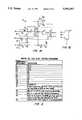
- FIG. 1Ais a diagram of a logic cell and its connections according to one embodiment of the present invention
- FIG. 1Bis symbolic representation of the logic cell of FIG. 1A.
- FIG. 2is a table of programmable switches and their operation with respect to the logic cell of FIG. 1A.
- FIG. 4Arepresents the logic cell of FIG. 1A as a latch
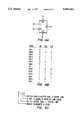
- FIG. 4Bis a list of 14 latch types possible with the logic cell
- FIG. 4Cis an explanation of the notation used in the list of FIG. 4B.
- FIG. 5Arepresents the logic cell 10 of FIG. 1A as a D-type flip-flop
- FIG. 5Bis a list of 28 different possibilities of D flip-flops possible with the logic cell
- FIG. 5Cis an explanation of the notation used in the list of FIG. 5B.
- FIG. 6illustrates an exemplary array of tiles, according to the present invention.
- FIG. 7Aillustrates local wiring segments in each tile of the array of FIG. 6;
- FIG. 7Billustrates the connections between the local wiring segments of FIG. 7A in an array of tiles.
- FIG. 8shows a tile in which the output terminal of the logic cell is not connectable to its input terminals through local wiring segments, according to another embodiment of the present invention.
- FIG. 9shows the tile local wiring segments connected to a logic cell with four input terminals, according to another embodiment of the present invention.
- FIG. 10Ashows the local wiring segments connected to a logic cell having a three-state buffer on the output terminal of the cell, according to still another embodiment of the present invention
- FIG. 10Bshows the programmable switches at all the intersections between vertical and horizontal local wiring segments, according to a variation of the tile of FIG. 10A
- FIG. 10Cdetails the local wiring segment connections in a 5 ⁇ 3 local region of FIG. 10B tiles.
- FIG. 11details the long wiring segments in an array of tiles of FIG. 6.
- FIG. 12Ais a representation of a passive programmable connection between the long wiring segments of FIG. 11;
- FIG. 12Bis a representation of an active programmable connection between the long wiring segments;
- FIG. 12Crepresents another active programmable connection.
- FIG. 13shows a distribution of active and passive programmable connections for a long wiring segment through several tiles.
- FIG. 14illustrates one technique of avoiding blockages on the long wiring segments in accordance with the present invention.
- FIG. 15illustrates another technique of avoiding blockages on the long wiring segments in accordance with the present invention.
- FIG. 16Aillustrates a connection between two logic cells in an array of such cells with a horizontal long wiring segment and a vertical long wiring segment;
- FIG. 16Billustrates a zig-zaged connection between the two logic cells with a more complex combination of long wiring segments.
- FIG. 17shows the horizontal global lines through a tile for the distribution of global signals through the array of tiles, according to the present invention.
- FIG. 18illustrates how two vertically adjacent tiles are connectable to the horizontal global lines in one of the tiles of FIG. 16.
- FIG. 19shows how the horizontal global lines are connected to vertical global lines to form a global wiring network for an array of tiles.
- FIG. 20illustrates the division of horizontal and vertical global lines into a sector for multiple and separate global networks in the tile array.
- FPGAsuse either memory cells or antifuses for the programmable switches. Memory cells are reprogrammable and antifuses are programmable only once.
- the present inventionis designed to be implemented with a new memory-type of programmable interconnect, as disclosed in a patent U.S. patent application No. 08/270,714, entitled, "A GENERAL PURPOSE, NON-VOLATILE REPROGRAMMABLE SWITCH,” filed Jul. 5, 1994 by Robert J. Lipp, Richard D. Freeman, Robert U. Broze, John M. Caywood, and Joseph G. Nolan, III, and assigned to the present assignee.
- NVMnon-volatile reprogrammable transistor memory
- the present inventionshould not be considered limited to the disclosed programmable switch only. Other types of memory cells may be used for the programmable switches. Even an antifuse-based FPGA may benefit from the present invention.
- the present inventionuses a logic cell 10, as shown in FIG. 1A.
- the logic cell 10has a core 17, which is denoted by a dotted line.
- the core 17has an inverter 11 which has an output node connected to the control nodes of two transfer gates 12 and 13.
- Each transfer gateis basically a PMOS and an NMOS transistor having a first common source/drain region forming the input node to the transfer gate and a second common source/drain region forming an output node of the transfer gate.
- the gate electrodes for the PMOS and NMOS transistorsform the two control nodes.
- the output nodes of the transfer gates 12 and 13are connected in common to an input node of a NAND gate 14.
- the output node of the NAND gate 14is connected to input nodes of an inverter 15 and an optional inverter 16, which is connected in parallel to the first inverter 15.
- the inverters 15 and 16act as buffers for the output signal from the NAND gate 14.
- the signals on the output nodes of the inverters 15 and 16are the same and, for the remainder of this disclosure, are considered as the output signal on the output terminal Y of the logic cell 10.
- the second inverter 16is used for particular loads on the wiring routing from the output terminal Y. This is explained below. It should be noted that the logic cell core 17 itself contains no programmable elements; rather, the input signals to the core are controlled by programmable switches located outside the core 17 to define the function of the cell 10.
- the logic cell 10has three input terminals, X2, X3, and X1, in descending order in the drawing.
- the input terminal X2is connected to the input node of an inverter 43 which has its output node connected to the input node of the inverter 11 of the logic cell core by a programmable switch 25.
- the input terminal X2is connectable to ground.
- the input terminal X2is also connectable directly to the input node of the inverter 11.
- the input node of the inverter 11is also connected to the PMOS gate electrode of the transfer gate 12 and the gate electrode of the NMOS transistor of the transfer gate 13.
- the input terminal X3is connected to the input node of an inverter 42, which has its output node connectable to the input terminal of the transfer gate 13 through a programmable switch 27. Through another programmable switch 26, the input terminal X3 is also connectable directly to the input node of the transfer gate 13. The input node X3 is also connectable to ground through a programmable switch 22.
- the input terminal X1is connected to the input node of an inverter 41 which has its output node connectable to the second input node of the NAND gate 14 through programmable switches 29 and 35.
- a programmable switch 28which is connected in parallel to the inverter 41 and programmable switch 29, the input terminal X1 is directly connectable to the second input terminal of the NAND gate 14 through the programmable switch 35.
- the second input terminal of the NAND gate 14is also capable of being pulled high (the positive power supply at V CC ) through a programmable switch 34. Similar to the previous input terminals X2 and X3, the input terminal X1 is also capable of being set low (the lower power supply at ground) by a programmable switch 21.
- the output terminal F from the inverter 15is also connectable to the input node of the transfer gate 12 through a programmable switch 30.
- the input terminal of the transfer gate 12is also capable of being set high by a programmable switch 32, or set low by a programmable switch 33.
- the input terminal of the transfer gate 12is also connectable to the input terminal X1 through a programmable switch 31, which is connected between the programmable switches 28, 29, and 35.
- FIG. 1BA representation of the logic cell 10 as used in subsequent drawings is shown in FIG. 1B. While the other embodiments of the present invention have other number of input terminals, three input terminals are believed to be optimum based upon calculations of likely configurations.
- the cell 10is much smaller than the cells of most of the present FPGAs. This allows a greater packing density, i.e., less area per cell, on the integrated circuit.
- the logic cell 10has great versatility and is capable of performing many functions.
- the table in FIG. 2illustrates the functions of the different programmable switches in the logic cell 10.
- the transfer gates 12 and 13operate as a simple multiplexer.
- the input signal to the transfer gate 12is described as the input signal A and the input signal to the transfer gate 13 as the input signal B.
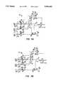
- FIG. 3Aillustrates the setting of the programmable switches so that the logic cell 10 operates as a two-input AND gate.
- the programmable switchesare labelled as "ON” to make the connection, while they are labelled as “OFF” to indicate that the programmable switch remains open.
- the two AND gate inputsare the signals on the X1 and X3 input terminals.
- the programmable switches for the X2 input terminal, i.e., programmable switches 23 and 25,have been set to insure that the transfer gate 13 passes the signal on the input terminal X3 to the first input node of the NAND gate 14.
- FIG. 3Billustrates another setting of the programmable switches so that the logic cell 10 operates as a D-latch with an active high clear (CLR) control signal.
- the data signal for the latchis received by the X3 input terminal and the clear signal by the X1 input terminal.
- the programmable switch 25 for the X2 input terminalis set to turn on the transfer gates 12 and 13.
- the programmable switch 30is turned on for a feedback from the output terminal of the logic cell to complete the latch.
- FIG. 4Aillustrates the logic cell 10 drawn as a latch.
- FIG. 4Bis a list of 14 latch types which are possible with the logic cell 10, and
- FIG. 4Cexplains the latch-type notation used in FIG. 4B.
- FIG. 5Ais a representation of the logic cell 10 configured as a D-type flip-flop.
- FIG. 5Blists 28 different possibilities of D flip-flops which are possible with the logic cell 10.
- FIG. 5Cexplains the notation used to denote the different types of flip-flops in FIG. 5B.
- one logic cell 10cannot be configured to perform the desired function, more than one cell may be connected together and programmed. To make these connections, the wiring of the FPGA comes into play.
- any placement and routing architecture of wiring between logic cells in an FPGAis a balance. If a designer has infinite line and switch resources, a full crossbar network which allows the output of every cell to access the input of every cell would be the best architecture. However, simple calculations indicate that the required number of programmable switches only would occupy an inordinate amount of space, even in a array with a moderate number of logic cells. Additionally, a calculation of the average switch utilization indicates that most of the switches would not be used. On the other hand, if a routing architecture is restricted so that each cell output can only be routed to a set of inputs of a single cell, nearly any circuit which would be desired by a user could not be configured.
- the present inventionminimizes the wiring resources, i.e., the wiring segments to and from the input and output terminals of the logic cells and the programmable switches for interconnecting the segments, with a maximization of the number of routable connections.
- the present inventionachieves these goals by the use of overlapping windows of tiles, directional routing and programmable interconnecting tiles to make an extremely adaptable routing architecture.
- the word "tile"refers to a logic cell and its associated wiring segments and programmable switches.
- An array of tilesforms the FPGA.
- the routing architecture of the tiles of the present inventionare divisible into three components, local routing, long routing, and global routing.
- each 3 ⁇ 3 region of tilesoverlaps in a manner such that the routing of the wiring segments in each tile are "self-similar" for each focal, i.e., center, tile in the 3 ⁇ 3 region.
- the focal tilemoves with the 3 ⁇ 3 region, which can be anywhere in the array of tiles.
- self-similarmeans that the output of any focal tile can always reach the input of any other cell (including itself), in its 3 ⁇ 3 region of tiles by a unique, guaranteed route.
- FIG. 6illustrates this point with an exemplary array of tiles 40.
- each tile 40has a logic cell 10 and its associated wiring segments and programming switches.
- a solid line 41closes a 3 ⁇ 3 region of tiles.
- the focal tile of this regionis denoted F1.
- the output of the logic cell of F1can reach the input of any logic cell of any tile in the region enclosed by the line 41 by a unique, guaranteed route.
- another 3 ⁇ 3 regionis considered, here indicated by a solid line 42, with the focal tile of this region denoted F2
- the output of the logic cell in F2can reach the input of any logic cell within the region denoted by line 42 by a unique, guaranteed route.
- the regions denoted by the lines 41 and 42are overlapping and that every tile in the array (except for those at the periphery) are focal tiles.
- FIG. 7Aillustrates the local routing architecture of a single tile 40 according to one embodiment of the present invention.
- the input terminals X1, X2 and X3 of the logic cell 10 of the tile 40are connected to three wiring segments, which are part of a set of nine vertical local wiring segments 43.
- the output terminal Y of the logic cell 10is connected to one of the three horizontal local wiring segments 44.
- At the intersection of each of the vertical local wiring segments 43 and horizontal local wiring segments 44are programmable switches, which are indicated by open circles.
- the local wiring segments 43 and 44 of adjacent tilesconnect in an overlapping manner.
- the top two segments at the right edge of the tileare connected to horizontal wiring segments 44 in horizontally adjacent tiles.
- Overlapoccurs because in each tile, the bottom two segments become the two segments as one proceeds from right to left across the tile 40.
- For the vertical local wiring segments 43six of the nine wiring segments are connected to segments 43 in vertically adjacent tiles. At the bottom of each tile 40, the six segments are the first, second, fourth, fifth, seventh and eighth from the left. Overlap occurs because in each tile 40 these segments were respectively the second, third, fifth, sixth, eight and ninth segments before reaching the bottom of the tile.
- FIG. 7Bshows the connections of the local wiring segments 43 and 44 in a 3 ⁇ 3 tile region.
- the tile 40Eis the focal tile of the region and its output terminal may be connected to any input terminal of a logic cell in any neighboring tile 40A-40D, 40F-40I, and itself through a single, unique programmable switch.
- Each logic cell of a focal tilehas a new set of routing resources identical to its neighbors. In this embodiment, the new wiring are guaranteed to be available.
- the output of the logic cell of the focal tilecan reach any or all of the 27 inputs of the neighboring logic cells, including itself.
- the ability to reach these nine cellsgives substantially more routability than is found typically in the prior art, which only allowed local connections to the four adjacent orthogonal logic cells. In the present case, the placement of functions with specific logic cells is much less constrained and the percentage of routes which may be accomplished with local routing resources is larger.
- each tile 40has the same arrangement of vertical local wiring segments 45 and horizontal wiring segments 46, as shown in FIG. 7A.
- the three programmable switches at the intersections of the vertical wiring segments connected to the local cell input terminals X1, X2 and X3, and the horizontal wiring segment connected to the output terminal Fhave been eliminated, as shown in FIG. 8.
- the output terminal of the logic cell of the focal tilemay be connected to the input terminals of its eight adjacent neighbors, but not to the input terminals of its own logic cell. In typical applications there are very few signals which feed back to their own logic cell. If required, this feedback path may be implemented, either internally to the logic cell (note programmable switch 30 in FIG. 1A), or by the use of a long routing resource, discussed below.
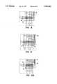
- FIG. 9illustrates local routing with a logic cell 10A having four input terminals X1, X2, X3, X4, and a single output Y.
- the horizontal local wiring segments 48remain at three with the output terminal Y connected to one of the segments as before.
- each local connectionrequires only one programmable switch. This contributes to the speed of the circuit implemented on this local "mesh" of wiring segments, since the interconnect speed is an inverse function of the number of programmable switches a signal traverses.
- the local routing as described thus farhas one drawback. If a local cell output terminal does not need a connection to an input terminal of cell in one of the tiles of the local region, that path is wasted. In the worst case, an unused logic cell leaves 27 unused paths. To correct this deficiency, the local routing architecture may be modified slightly so that the output terminal of a logic cell is not required to use the local wiring segments. This permits the local wiring segments to be used for other connections; routability in the architecture is increased.
- FIGS. 10A and 10BDifferent modifications are shown in FIGS. 10A and 10B.
- a three-state driver 49is added at the output terminal Y of the logic cell 10.
- the driver 49is enabled or disabled by a programmable interconnect, not shown.
- the driver 49is disabled, the logic cell is effectively disconnected from the horizontal wiring segments 44.
- the driver 49is enabled, it drives the high or low logic signals from the logic cell 10 onto the connected horizontal wiring segment 44.
- each of the horizontal wiring segments 44are connectable to the output terminal Y of the logic cell 10 by programmable switches.
- a dotted line 50encircles the programmable switches at the intersection of the output terminal Y and the horizontal wiring segments 44.
- FIG. 10Cillustrates the detailed local wiring segments in a 5 ⁇ 3 tile region with the focal cell of this region indicated.
- larger local tile regionsmay be assembled, e.g., 4 ⁇ 4, 5 ⁇ 5 and other regions. Moreover, these regions need not be square, such as 3 ⁇ 4, 4 ⁇ 5, 3 ⁇ 5 tile regions. Of course, each increased region increases the percentage of connections which can be made locally.
- each of the tileshas additional programmable routing resources so that connections can be made to nodes outside the local regions.
- These so-called long routing resourcesare completely programmable and are not shared with the local wiring segments. Approximately 66% of all routing can be made by the local routing resources; the remaining 33% can be performed by the long routing resources.
- the long wiring segments of the present inventionalso allows better control over the maximum path length of connected wiring, and hence the timing of signals, compared to the prior art.
- a traditional gate array with a similar capacity to the FPGA herein describedrequires approximately 9 ⁇ 12 tracks in the gate array's channels to attain 80% routability to all of the array's resources. Since 66% of the routing is being handled by the local routing resources of the FPGA of the present invention, only 3 ⁇ 4 tracks are required for long routing. To insure ample routability, slightly more long wiring segments are used.
- the presentuses five horizontal long wiring segments 51 and five vertical long wiring segments 52, the long routing resources in each tile 40.
- the horizontal long wiring segments 51are programmably connectable to the output terminal Y of the logic cell 10 of the tile by programmable switches, which are enclosed by a dotted box 60.
- the horizontal and vertical long wiring segments 51 and 52are each programmably connectable by programmable switches, indicated by a dotted box 61 at the intersection of the vertical and horizontal long wiring segments.
- Each of the input terminals X1, X2, and X3 of the logic cellare connectable to the vertical wiring segments 52 by programmable interconnects enclosed by a dotted box 62.
- a programmable connectionis placed.
- the state of the programmable connectiondetermines whether a long wiring segment, vertical and horizontal, continues across to an adjacent tile.
- the programmable connections for the horizontal wiring segments 51are enclosed by a dotted box 64; for the vertical wiring segments 52, the programmable connections are enclosed by a dotted box 63.
- These programmable connectionsallow for an optimal line length to be decided.
- every long wiring segmenthas a programmable connection at the boundary of each tile 40. This arrangement effectively implements a channel routing architecture like a traditional gate array routing with minimum waste.
- the programmable connections for the long wiring segmentsare implemented in two general ways.
- the firstis a passive programmable connection which is a single programmable switch which can interconnect two long wiring segments as shown in FIG. 12A.
- the other type of programmable connectionis an active programmable connection, such as shown in FIG. 12B.
- the active programmable connectionhas two buffers 65 and 66 arranged in opposite directions. Two programmable switches 66 and 68 make the connection to the output nodes of the buffers 65 and 67.
- the connectionis programmably bidirectional. If a programmable connection with only one buffer is required, an alternative is shown in FIG. 12C.
- a buffer 69has two programmable switches 71 and 72, which make the connections to the input nodes of the long wiring segments on either side of the buffer 69.
- Programmable interconnects 73 and 74make the connection to the output node of the buffer 69 to the long wiring segments.
- Each long horizontal wiring segmenthas an active programmable connection 80 every five tiles and intermediate passive programmable connections 81 in the other tiles. There are thus two buffers and two programmable switches for the horizontal long wiring segments 51 in each tile 40.
- the long vertical wiring segments 52contribute two more programmable buffers and switches to each tile 40. Thus, only four buffers and four programmable switches are added per tile.
- the worst case number of programmable switches which (in the programmable connecting array) may be drivenis five horizontally (the extra programmable switch occurs because the first switch is at the output of the buffer), and four on the vertical wiring segments.
- the worst case number of programmable switches which (in the programmable connecting array) may be drivenis five horizontally (the extra programmable switch occurs because the first switch is at the output of the buffer), and four on the vertical wiring segments.
- the worst case number of programmable switches which (in the programmable connecting array) may be drivenis five horizontally (the extra programmable switch occurs because the first switch is at the output of the buffer), and four on the vertical wiring segments.
- the signalis inverted when it reaches the input terminal of the cell, if the signal has passed through an odd number of active programmable connections.
- the inverted signalmay be corrected by programming the logic cell to invert the incoming signal.
- routingcan be constrained to use paths with an even number of active programmable connections.
- FIG. 14illustrates a wiring segment 75 which is connected to the output terminal of the logic cell 10. (The extra load of the segment 75 may be handled by the parallel-connected inverter 16 shown in FIG. 1B.) The segment 75 extends upward into the tile above to intersect the horizontal long segments 51 of that tile.
- FIG. 14illustrates how the wiring segment 75 from the tile below which extends upwardly to cross the horizontal long wiring segments 51. There are programmable switches surrounded by a dotted ellipse 76, at the intersection of the wiring segment 75 and horizontal long wiring segments 51.
- FIG. 15illustrates programmable connections 77 for the long horizontal wiring segments and programmable connections 78 for the long vertical wiring segments 52.
- Each programmable connection 77 and 78allows a signal on its respective long wiring segment to "shuffle" over to a neighboring non-corresponding long wiring segment in the adjacent tile. For example, a signal on the top horizontal wiring segment 51, can be shuffled over to the second long horizontal wiring segment at the tile boundary, if there is a conflict or blockage with the top wiring segment in the adjacent tile.
- These programmable connections 77 and 78may be bidirectional or oriented to drive signals in one direction or another. It should be evident that these programmable connections do not necessarily have to make connections between neighboring wiring segments.
- Still another way of reducing blockagesis to reduce the directionality of these programmable connections. That is, as previously described and shown, programmable connections are made between a horizontal long wiring segment to a vertical long wiring segment or vice versa. Thus, the long wiring connections are only allowed to be "L-shaped" and give very predictable timing. The selection of wiring segments is sufficient to know the routing and length of the segments. By relaxing the directionality of the wiring segments, the connection can be zig-zagged from the source to the destination. This allows freedom to move from a different row and column if the desired one is too congested. This is very similar to that of a router for a traditional channelled gate array and the same type of optimization may be realized.
- FIGS. 16A and 16Billustrate this point.
- FIG. 16Aillustrates an array of logic cells 10 in which two logic cells are connected by a horizontal long wiring segment and a vertical long wiring segment. A typical "L-shape" is formed by the two connected long wiring segments.
- FIG. 16Billustrates a zig-zaged connection between the two logic cells. This connection avoids blockages, shown by dotted lines, which prevent the connection of FIG. 16A and other possible connection routes.
- the wiring for global signalspresents a difficult problem because there is typically no prior knowledge of where the global signals are required to go.
- the present inventionpartially solves this problem by designating each of the input terminals of the logic cell 10 for specified global signals.
- the input terminal X2may be used to receive a global block signal
- the input terminal X3may be used for either clock or multiplexer select signals.
- the wiring used to carry global signalsis separated from both the local and long wiring segments and the number of programmable switches for the global wiring is limited.
- the array of tilesis partitioned into sections by the global wiring which allow different sections to select how the global wiring in that section is to be utilized.
- Each of these wiresmay be connected to the X2 input terminal of each logic cell in the array. Additionally, through a programmable switch, one of the four global wires may be selected to be connected to the X1 input terminal of every logic cell within an array section.
- each tile 40has three global lines 81 running horizontally through it.
- the top two linesare connected to two of the possible four global wires.
- These horizontal lines 81are connectable to the X2 input terminals of two vertically adjacent tiles through programmable switches. That is, the X2 input terminal of the logic cell 10 containing the global lines 81 and the X2 input terminal of the logic cell 10 in the tile immediately below may be connected to the horizontal global lines 81 of the first tile.
- the tile belowhas a similar set of horizontal global lines 81 which are connected to the other two of the four main global lines. These lines 81 are connectable to the X2 input terminal of the logic cell 10 of that tile 40, and connectable to the input terminal of the logic cell in the tile below.
- FIG. 18illustrates how two vertically adjacent tiles are connectable to the top two lines of the horizontal global lines 81 by the darkened vertical wiring segment 82, one of the local vertical wiring segments 43.
- the bottom line of the horizontal global lines 81is connectable to the X1 input terminal of the logic cell in that tile only.
- the global linesdistribute signals through spines formed by vertical global lines 82 and 83, as shown in FIG. 19. From the pair of global lines 82 and the pair of global lines 84, four global signals may be distributed through the network. Each pair of vertical global lines 82 and 84 drives one pair, i.e., the top two lines, of the horizontal global lines 81 in alternate rows. The bottom line in the global lines 81 is connectable to any one of the four lines in the lines 81 and 84. As shown in FIG. 19, the lines 81 extend horizontally on either side of the vertical global lines 82 and 84. Each of the set of vertical lines 82 and 84 with the horizontal extensions of the lines 81 cover a sector of the array of tiles. This is shown in an example in FIG. 20, in which the global lines are labelled with the suffix A on the left sector, and the suffix B on the right sector. This allows the global distribution of signals to be designed so that the required skew characteristics of the signals may be met.
Landscapes
- Physics & Mathematics (AREA)
- Mathematical Physics (AREA)
- Engineering & Computer Science (AREA)
- Computer Hardware Design (AREA)
- Computing Systems (AREA)
- General Engineering & Computer Science (AREA)
- Computer Networks & Wireless Communication (AREA)
- Logic Circuits (AREA)
- Design And Manufacture Of Integrated Circuits (AREA)
Abstract
Description
Claims (35)
Priority Applications (7)
| Application Number | Priority Date | Filing Date | Title |
|---|---|---|---|
| US08/418,972US5594363A (en) | 1995-04-07 | 1995-04-07 | Logic cell and routing architecture in a field programmable gate array |
| EP96908832AEP0819340B1 (en) | 1995-04-07 | 1996-03-14 | Logic cell and routing architecture in a field programmable gate array |
| PCT/US1996/003599WO1996031950A1 (en) | 1995-04-07 | 1996-03-14 | Logic cell and routing architecture in a field programmable gate array |
| DE69638182TDE69638182D1 (en) | 1995-04-07 | 1996-03-14 | LOGICAL CELL AND CONNECTION ARCHITECTURE IN A USER PROGRAMMABLE LOGICAL FIELD |
| JP53030896AJP3645572B2 (en) | 1995-04-07 | 1996-03-14 | Logic cells and routing architecture in field programmable gate arrays |
| AU52543/96AAU5254396A (en) | 1995-04-07 | 1996-03-14 | Logic cell and routing architecture in a field programmable gate array |
| TW085110177ATW314653B (en) | 1995-04-07 | 1996-08-19 |
Applications Claiming Priority (1)
| Application Number | Priority Date | Filing Date | Title |
|---|---|---|---|
| US08/418,972US5594363A (en) | 1995-04-07 | 1995-04-07 | Logic cell and routing architecture in a field programmable gate array |
Publications (1)
| Publication Number | Publication Date |
|---|---|
| US5594363Atrue US5594363A (en) | 1997-01-14 |
Family
ID=23660283
Family Applications (1)
| Application Number | Title | Priority Date | Filing Date |
|---|---|---|---|
| US08/418,972Expired - LifetimeUS5594363A (en) | 1995-04-07 | 1995-04-07 | Logic cell and routing architecture in a field programmable gate array |
Country Status (7)
| Country | Link |
|---|---|
| US (1) | US5594363A (en) |
| EP (1) | EP0819340B1 (en) |
| JP (1) | JP3645572B2 (en) |
| AU (1) | AU5254396A (en) |
| DE (1) | DE69638182D1 (en) |
| TW (1) | TW314653B (en) |
| WO (1) | WO1996031950A1 (en) |
Cited By (94)
| Publication number | Priority date | Publication date | Assignee | Title |
|---|---|---|---|---|
| US5698992A (en) | 1986-09-19 | 1997-12-16 | Actel Corporation | Programmable logic module and architecture for field programmable gate array device |
| US5742181A (en)* | 1996-06-04 | 1998-04-21 | Hewlett-Packard Co. | FPGA with hierarchical interconnect structure and hyperlinks |
| US5781033A (en) | 1990-05-11 | 1998-07-14 | Actel Corporation | Logic module with configurable combinational and sequential blocks |
| US5838040A (en)* | 1997-03-31 | 1998-11-17 | Gatefield Corporation | Nonvolatile reprogrammable interconnect cell with FN tunneling in sense |
| US5936426A (en) | 1997-02-03 | 1999-08-10 | Actel Corporation | Logic function module for field programmable array |
| US6160420A (en) | 1986-09-19 | 2000-12-12 | Actel Corporation | Programmable interconnect architecture |
| US6272655B1 (en)* | 1998-06-11 | 2001-08-07 | Actel Corporation | Method of reducing test time for NVM cell-based FPGA |
| US6294926B1 (en) | 1999-07-16 | 2001-09-25 | Philips Electronics North America Corporation | Very fine-grain field programmable gate array architecture and circuitry |
| US6594810B1 (en) | 2001-10-04 | 2003-07-15 | M2000 | Reconfigurable integrated circuit with a scalable architecture |
| US20050041513A1 (en)* | 2000-07-05 | 2005-02-24 | Mosaic Systems, Inc. | Multi-level semiconductor memory architecture and method of forming the same |
| US6885218B1 (en)* | 2002-10-08 | 2005-04-26 | Actel Corporation | Parallel programmable antifuse field programmable gate array device (FPGA) and a method for programming and testing an antifuse FPGA |
| US20050146354A1 (en)* | 2002-12-18 | 2005-07-07 | Actel Corporation | Multi-level routing architecture in a field programmable gate array having transmitters and receivers |
| US20050206407A1 (en)* | 2002-06-04 | 2005-09-22 | Actel Corporation | Field-programmable gate array low voltage differential signaling driver utilizing two complimentary output buffers |
| US7075334B1 (en) | 2002-12-27 | 2006-07-11 | Actel Corporation | Repeatable block producing a non-uniform routing architecture in a field programmable gate array having segmented tracks |
| US20060190908A1 (en)* | 2003-06-25 | 2006-08-24 | Bajuk Stanislav P | Coding of FPGA and standard cell logic in a tiling structure |
| US20070057693A1 (en)* | 2005-09-13 | 2007-03-15 | M2000 | Reconfigurable circuit with redundant reconfigurable cluster(S) |
| US7212030B1 (en) | 2004-12-31 | 2007-05-01 | Actel Corporation | Field programmable gate array long line routing network |
| US20070118783A1 (en)* | 2005-11-23 | 2007-05-24 | M2000 Inc. | Runtime reconfiguration of reconfigurable circuits |
| EP1583238A3 (en)* | 2004-03-31 | 2007-07-11 | NEC Electronics Corporation | Semiconductor device having universal logic cell |
| US20070182446A1 (en)* | 2003-05-28 | 2007-08-09 | Actel Corporation | Synchronous first-in/first-out block memory for a field programmable gate array |
| US20080025091A1 (en)* | 2004-09-09 | 2008-01-31 | Actel Corporation | Non-volatile memory cells in a field programmable gate array |
| WO2008013098A1 (en) | 2006-07-27 | 2008-01-31 | Panasonic Corporation | Semiconductor integrated circuit, program converting apparatus and mapping apparatus |
| US7378867B1 (en) | 2002-06-04 | 2008-05-27 | Actel Corporation | Field-programmable gate array low voltage differential signaling driver utilizing two complimentary output buffers |
| US7385419B1 (en) | 2003-05-30 | 2008-06-10 | Actel Corporation | Dedicated input/output first in/first out module for a field programmable gate array |
| US20090009215A1 (en)* | 2004-05-12 | 2009-01-08 | Matsumoto Yohei | Integrated Circuit with Multidimensional Switch Topology |
| US7549138B2 (en) | 2002-10-08 | 2009-06-16 | Actel Corporation | Parallel programmable antifuse field programmable gate array device (FPGA) and a method for programming and testing an antifuse FPGA |
| US7579869B2 (en) | 2002-12-27 | 2009-08-25 | Actel Corporation | Repeatable block producing a non-uniform routing architecture in a field programmable gate array having segmented tracks |
| US20090256590A1 (en)* | 2008-04-10 | 2009-10-15 | Silicon Storage Technology, Inc. | Storage element for controlling a logic circuit, and a logic device having an array of such storage elements |
| US20100095147A1 (en)* | 2005-09-13 | 2010-04-15 | Abound Logic, S.A.S. | Reconfigurable circuit with redundant reconfigurable cluster(s) |
| US20100308863A1 (en)* | 2004-03-24 | 2010-12-09 | Gliese Joerg | Architecture of Function Blocks and Wirings in a Structured ASIC and Configurable Driver Cell of a Logic Cell Zone |
| US8374018B2 (en) | 2010-07-09 | 2013-02-12 | Crossbar, Inc. | Resistive memory using SiGe material |
| US8391049B2 (en) | 2010-09-29 | 2013-03-05 | Crossbar, Inc. | Resistor structure for a non-volatile memory device and method |
| US8394670B2 (en) | 2011-05-31 | 2013-03-12 | Crossbar, Inc. | Vertical diodes for non-volatile memory device |
| US8404553B2 (en) | 2010-08-23 | 2013-03-26 | Crossbar, Inc. | Disturb-resistant non-volatile memory device and method |
| US8441835B2 (en) | 2010-06-11 | 2013-05-14 | Crossbar, Inc. | Interface control for improved switching in RRAM |
| US8450209B2 (en) | 2010-11-05 | 2013-05-28 | Crossbar, Inc. | p+ Polysilicon material on aluminum for non-volatile memory device and method |
| US8450710B2 (en) | 2011-05-27 | 2013-05-28 | Crossbar, Inc. | Low temperature p+ silicon junction material for a non-volatile memory device |
| US8467227B1 (en) | 2010-11-04 | 2013-06-18 | Crossbar, Inc. | Hetero resistive switching material layer in RRAM device and method |
| US8492195B2 (en) | 2010-08-23 | 2013-07-23 | Crossbar, Inc. | Method for forming stackable non-volatile resistive switching memory devices |
| US8519485B2 (en) | 2010-06-11 | 2013-08-27 | Crossbar, Inc. | Pillar structure for memory device and method |
| US8558212B2 (en) | 2010-09-29 | 2013-10-15 | Crossbar, Inc. | Conductive path in switching material in a resistive random access memory device and control |
| US8659929B2 (en) | 2011-06-30 | 2014-02-25 | Crossbar, Inc. | Amorphous silicon RRAM with non-linear device and operation |
| US8658476B1 (en) | 2012-04-20 | 2014-02-25 | Crossbar, Inc. | Low temperature P+ polycrystalline silicon material for non-volatile memory device |
| US8716098B1 (en) | 2012-03-09 | 2014-05-06 | Crossbar, Inc. | Selective removal method and structure of silver in resistive switching device for a non-volatile memory device |
| US8765566B2 (en) | 2012-05-10 | 2014-07-01 | Crossbar, Inc. | Line and space architecture for a non-volatile memory device |
| US8791010B1 (en) | 2010-12-31 | 2014-07-29 | Crossbar, Inc. | Silver interconnects for stacked non-volatile memory device and method |
| US8796658B1 (en) | 2012-05-07 | 2014-08-05 | Crossbar, Inc. | Filamentary based non-volatile resistive memory device and method |
| US8809831B2 (en) | 2010-07-13 | 2014-08-19 | Crossbar, Inc. | On/off ratio for non-volatile memory device and method |
| US8815696B1 (en) | 2010-12-31 | 2014-08-26 | Crossbar, Inc. | Disturb-resistant non-volatile memory device using via-fill and etchback technique |
| US8884261B2 (en) | 2010-08-23 | 2014-11-11 | Crossbar, Inc. | Device switching using layered device structure |
| US8889521B1 (en) | 2012-09-14 | 2014-11-18 | Crossbar, Inc. | Method for silver deposition for a non-volatile memory device |
| US8930174B2 (en) | 2010-12-28 | 2015-01-06 | Crossbar, Inc. | Modeling technique for resistive random access memory (RRAM) cells |
| US8934280B1 (en) | 2013-02-06 | 2015-01-13 | Crossbar, Inc. | Capacitive discharge programming for two-terminal memory cells |
| US8946669B1 (en) | 2012-04-05 | 2015-02-03 | Crossbar, Inc. | Resistive memory device and fabrication methods |
| US8947908B2 (en) | 2010-11-04 | 2015-02-03 | Crossbar, Inc. | Hetero-switching layer in a RRAM device and method |
| US8946046B1 (en) | 2012-05-02 | 2015-02-03 | Crossbar, Inc. | Guided path for forming a conductive filament in RRAM |
| US8946673B1 (en) | 2012-08-24 | 2015-02-03 | Crossbar, Inc. | Resistive switching device structure with improved data retention for non-volatile memory device and method |
| US8982647B2 (en) | 2012-11-14 | 2015-03-17 | Crossbar, Inc. | Resistive random access memory equalization and sensing |
| US9012307B2 (en)* | 2010-07-13 | 2015-04-21 | Crossbar, Inc. | Two terminal resistive switching device structure and method of fabricating |
| US20150178897A1 (en)* | 2012-07-03 | 2015-06-25 | Fotonation Limited | Method And System For Correcting A Distorted Input Image |
| US9087576B1 (en) | 2012-03-29 | 2015-07-21 | Crossbar, Inc. | Low temperature fabrication method for a three-dimensional memory device and structure |
| US9112145B1 (en) | 2013-01-31 | 2015-08-18 | Crossbar, Inc. | Rectified switching of two-terminal memory via real time filament formation |
| US20150262344A1 (en)* | 2012-07-03 | 2015-09-17 | Fotonation Limited | Method And System For Correcting A Distorted Input Image |
| US9153531B1 (en) | 2014-02-27 | 2015-10-06 | Altera Corporation | Methods and apparatus for reducing crosstalk and twist region height in routing wires |
| US9153623B1 (en) | 2010-12-31 | 2015-10-06 | Crossbar, Inc. | Thin film transistor steering element for a non-volatile memory device |
| US9191000B2 (en) | 2011-07-29 | 2015-11-17 | Crossbar, Inc. | Field programmable gate array utilizing two-terminal non-volatile memory |
| US9252191B2 (en) | 2011-07-22 | 2016-02-02 | Crossbar, Inc. | Seed layer for a p+ silicon germanium material for a non-volatile memory device and method |
| US9312483B2 (en) | 2012-09-24 | 2016-04-12 | Crossbar, Inc. | Electrode structure for a non-volatile memory device and method |
| US9324942B1 (en) | 2013-01-31 | 2016-04-26 | Crossbar, Inc. | Resistive memory cell with solid state diode |
| US9401475B1 (en) | 2010-08-23 | 2016-07-26 | Crossbar, Inc. | Method for silver deposition for a non-volatile memory device |
| US9406379B2 (en) | 2013-01-03 | 2016-08-02 | Crossbar, Inc. | Resistive random access memory with non-linear current-voltage relationship |
| US9412790B1 (en) | 2012-12-04 | 2016-08-09 | Crossbar, Inc. | Scalable RRAM device architecture for a non-volatile memory device and method |
| US9543359B2 (en) | 2011-05-31 | 2017-01-10 | Crossbar, Inc. | Switching device having a non-linear element |
| US9564394B1 (en) | 2014-11-18 | 2017-02-07 | Altera Corporation | Methods and apparatus for reducing spatial overlap between routing wires |
| US9564587B1 (en) | 2011-06-30 | 2017-02-07 | Crossbar, Inc. | Three-dimensional two-terminal memory with enhanced electric field and segmented interconnects |
| US9570678B1 (en) | 2010-06-08 | 2017-02-14 | Crossbar, Inc. | Resistive RAM with preferental filament formation region and methods |
| US9576616B2 (en) | 2012-10-10 | 2017-02-21 | Crossbar, Inc. | Non-volatile memory with overwrite capability and low write amplification |
| US9583701B1 (en) | 2012-08-14 | 2017-02-28 | Crossbar, Inc. | Methods for fabricating resistive memory device switching material using ion implantation |
| USRE46335E1 (en) | 2010-11-04 | 2017-03-07 | Crossbar, Inc. | Switching device having a non-linear element |
| US9601690B1 (en) | 2011-06-30 | 2017-03-21 | Crossbar, Inc. | Sub-oxide interface layer for two-terminal memory |
| US9601692B1 (en) | 2010-07-13 | 2017-03-21 | Crossbar, Inc. | Hetero-switching layer in a RRAM device and method |
| US9620206B2 (en) | 2011-05-31 | 2017-04-11 | Crossbar, Inc. | Memory array architecture with two-terminal memory cells |
| US9627443B2 (en) | 2011-06-30 | 2017-04-18 | Crossbar, Inc. | Three-dimensional oblique two-terminal memory with enhanced electric field |
| US9633723B2 (en) | 2011-06-23 | 2017-04-25 | Crossbar, Inc. | High operating speed resistive random access memory |
| US9685608B2 (en) | 2012-04-13 | 2017-06-20 | Crossbar, Inc. | Reduced diffusion in metal electrode for two-terminal memory |
| US9729155B2 (en) | 2011-07-29 | 2017-08-08 | Crossbar, Inc. | Field programmable gate array utilizing two-terminal non-volatile memory |
| US9735358B2 (en) | 2012-08-14 | 2017-08-15 | Crossbar, Inc. | Noble metal / non-noble metal electrode for RRAM applications |
| US9741765B1 (en) | 2012-08-14 | 2017-08-22 | Crossbar, Inc. | Monolithically integrated resistive memory using integrated-circuit foundry compatible processes |
| US20180081845A1 (en)* | 2016-09-16 | 2018-03-22 | Hewlett Packard Enterprise Development Lp | Crossbar Switch |
| US10056907B1 (en) | 2011-07-29 | 2018-08-21 | Crossbar, Inc. | Field programmable gate array utilizing two-terminal non-volatile memory |
| WO2019030899A1 (en)* | 2017-08-10 | 2019-02-14 | Nec Corporation | Routing network for reconfigurable circuit |
| CN109344541A (en)* | 2018-10-31 | 2019-02-15 | 京微齐力(北京)科技有限公司 | A method of wiring direction is determined according to area routing crowding |
| US10290801B2 (en) | 2014-02-07 | 2019-05-14 | Crossbar, Inc. | Scalable silicon based resistive memory device |
| US11068620B2 (en) | 2012-11-09 | 2021-07-20 | Crossbar, Inc. | Secure circuit integrated with memory layer |
Families Citing this family (2)
| Publication number | Priority date | Publication date | Assignee | Title |
|---|---|---|---|---|
| US6407576B1 (en) | 1999-03-04 | 2002-06-18 | Altera Corporation | Interconnection and input/output resources for programmable logic integrated circuit devices |
| JP4487738B2 (en)* | 2004-11-17 | 2010-06-23 | ソニー株式会社 | Semiconductor integrated circuit |
Citations (7)
| Publication number | Priority date | Publication date | Assignee | Title |
|---|---|---|---|---|
| US5245227A (en)* | 1990-11-02 | 1993-09-14 | Atmel Corporation | Versatile programmable logic cell for use in configurable logic arrays |
| US5430390A (en)* | 1991-03-06 | 1995-07-04 | Quicklogic Corporation | Programmable application specific integrated circuit and logic cell therefor |
| US5451887A (en)* | 1986-09-19 | 1995-09-19 | Actel Corporation | Programmable logic module and architecture for field programmable gate array device |
| US5477165A (en)* | 1986-09-19 | 1995-12-19 | Actel Corporation | Programmable logic module and architecture for field programmable gate array device |
| US5479113A (en)* | 1986-09-19 | 1995-12-26 | Actel Corporation | User-configurable logic circuits comprising antifuses and multiplexer-based logic modules |
| US5498978A (en)* | 1993-05-07 | 1996-03-12 | Kabushiki Kaisha Toshiba | Field programmable gate array |
| US5504440A (en)* | 1994-01-27 | 1996-04-02 | Dyna Logic Corporation | High speed programmable logic architecture |
Family Cites Families (8)
| Publication number | Priority date | Publication date | Assignee | Title |
|---|---|---|---|---|
| US4870302A (en)* | 1984-03-12 | 1989-09-26 | Xilinx, Inc. | Configurable electrical circuit having configurable logic elements and configurable interconnects |
| US4642487A (en)* | 1984-09-26 | 1987-02-10 | Xilinx, Inc. | Special interconnect for configurable logic array |
| US4758745B1 (en)* | 1986-09-19 | 1994-11-15 | Actel Corp | User programmable integrated circuit interconnect architecture and test method |
| US5185706A (en)* | 1989-08-15 | 1993-02-09 | Advanced Micro Devices, Inc. | Programmable gate array with logic cells having configurable output enable |
| US5212652A (en)* | 1989-08-15 | 1993-05-18 | Advanced Micro Devices, Inc. | Programmable gate array with improved interconnect structure |
| US5317209A (en)* | 1991-08-29 | 1994-05-31 | National Semiconductor Corporation | Dynamic three-state bussing capability in a configurable logic array |
| EP0647030A3 (en) | 1993-09-30 | 1995-11-08 | Texas Instruments Inc | Integrated circuit devices. |
| US5465055A (en) | 1994-10-19 | 1995-11-07 | Crosspoint Solutions, Inc. | RAM-logic tile for field programmable gate arrays |
- 1995
- 1995-04-07USUS08/418,972patent/US5594363A/ennot_activeExpired - Lifetime
- 1996
- 1996-03-14WOPCT/US1996/003599patent/WO1996031950A1/enactiveApplication Filing
- 1996-03-14JPJP53030896Apatent/JP3645572B2/ennot_activeExpired - Fee Related
- 1996-03-14DEDE69638182Tpatent/DE69638182D1/ennot_activeExpired - Lifetime
- 1996-03-14EPEP96908832Apatent/EP0819340B1/ennot_activeExpired - Lifetime
- 1996-03-14AUAU52543/96Apatent/AU5254396A/ennot_activeAbandoned
- 1996-08-19TWTW085110177Apatent/TW314653B/zhnot_activeIP Right Cessation
Patent Citations (7)
| Publication number | Priority date | Publication date | Assignee | Title |
|---|---|---|---|---|
| US5451887A (en)* | 1986-09-19 | 1995-09-19 | Actel Corporation | Programmable logic module and architecture for field programmable gate array device |
| US5477165A (en)* | 1986-09-19 | 1995-12-19 | Actel Corporation | Programmable logic module and architecture for field programmable gate array device |
| US5479113A (en)* | 1986-09-19 | 1995-12-26 | Actel Corporation | User-configurable logic circuits comprising antifuses and multiplexer-based logic modules |
| US5245227A (en)* | 1990-11-02 | 1993-09-14 | Atmel Corporation | Versatile programmable logic cell for use in configurable logic arrays |
| US5430390A (en)* | 1991-03-06 | 1995-07-04 | Quicklogic Corporation | Programmable application specific integrated circuit and logic cell therefor |
| US5498978A (en)* | 1993-05-07 | 1996-03-12 | Kabushiki Kaisha Toshiba | Field programmable gate array |
| US5504440A (en)* | 1994-01-27 | 1996-04-02 | Dyna Logic Corporation | High speed programmable logic architecture |
Cited By (142)
| Publication number | Priority date | Publication date | Assignee | Title |
|---|---|---|---|---|
| US6160420A (en) | 1986-09-19 | 2000-12-12 | Actel Corporation | Programmable interconnect architecture |
| US5698992A (en) | 1986-09-19 | 1997-12-16 | Actel Corporation | Programmable logic module and architecture for field programmable gate array device |
| US5781033A (en) | 1990-05-11 | 1998-07-14 | Actel Corporation | Logic module with configurable combinational and sequential blocks |
| US5742181A (en)* | 1996-06-04 | 1998-04-21 | Hewlett-Packard Co. | FPGA with hierarchical interconnect structure and hyperlinks |
| US5936426A (en) | 1997-02-03 | 1999-08-10 | Actel Corporation | Logic function module for field programmable array |
| US5838040A (en)* | 1997-03-31 | 1998-11-17 | Gatefield Corporation | Nonvolatile reprogrammable interconnect cell with FN tunneling in sense |
| US6272655B1 (en)* | 1998-06-11 | 2001-08-07 | Actel Corporation | Method of reducing test time for NVM cell-based FPGA |
| US6294926B1 (en) | 1999-07-16 | 2001-09-25 | Philips Electronics North America Corporation | Very fine-grain field programmable gate array architecture and circuitry |
| US7020001B2 (en)* | 2000-07-05 | 2006-03-28 | Mosaic Systems, Inc. | Multi-level semiconductor memory architecture and method of forming the same |
| US20050041513A1 (en)* | 2000-07-05 | 2005-02-24 | Mosaic Systems, Inc. | Multi-level semiconductor memory architecture and method of forming the same |
| US6594810B1 (en) | 2001-10-04 | 2003-07-15 | M2000 | Reconfigurable integrated circuit with a scalable architecture |
| US20050206407A1 (en)* | 2002-06-04 | 2005-09-22 | Actel Corporation | Field-programmable gate array low voltage differential signaling driver utilizing two complimentary output buffers |
| US20080197905A1 (en)* | 2002-06-04 | 2008-08-21 | Actel Corporation | Field-programmable gate array low voltage differential signaling driver utilizing two complimentary output buffers |
| US7378867B1 (en) | 2002-06-04 | 2008-05-27 | Actel Corporation | Field-programmable gate array low voltage differential signaling driver utilizing two complimentary output buffers |
| US7119573B2 (en) | 2002-06-04 | 2006-10-10 | Actel Corporation | Field-programmable gate array low voltage differential signaling driver utilizing two complimentary output buffers |
| US7545166B2 (en) | 2002-06-04 | 2009-06-09 | Actel Corporation | Field-programmable gate array low voltage differential signaling driver utilizing two complimentary output buffers |
| US7549138B2 (en) | 2002-10-08 | 2009-06-16 | Actel Corporation | Parallel programmable antifuse field programmable gate array device (FPGA) and a method for programming and testing an antifuse FPGA |
| US6885218B1 (en)* | 2002-10-08 | 2005-04-26 | Actel Corporation | Parallel programmable antifuse field programmable gate array device (FPGA) and a method for programming and testing an antifuse FPGA |
| US7111272B1 (en) | 2002-10-08 | 2006-09-19 | Actel Corporation | Parallel programmable antifuse field programmable gate array device (FPGA) and a method for programming and testing an antifuse FPGA |
| US7126374B2 (en) | 2002-12-18 | 2006-10-24 | Actel Corporation | Multi-level routing architecture in a field programmable gate array having transmitters and receivers |
| US20050146354A1 (en)* | 2002-12-18 | 2005-07-07 | Actel Corporation | Multi-level routing architecture in a field programmable gate array having transmitters and receivers |
| US7579869B2 (en) | 2002-12-27 | 2009-08-25 | Actel Corporation | Repeatable block producing a non-uniform routing architecture in a field programmable gate array having segmented tracks |
| US7075334B1 (en) | 2002-12-27 | 2006-07-11 | Actel Corporation | Repeatable block producing a non-uniform routing architecture in a field programmable gate array having segmented tracks |
| US20070182446A1 (en)* | 2003-05-28 | 2007-08-09 | Actel Corporation | Synchronous first-in/first-out block memory for a field programmable gate array |
| US7394289B2 (en) | 2003-05-28 | 2008-07-01 | Actel Corporation | Synchronous first-in/first-out block memory for a field programmable gate array |
| US7385419B1 (en) | 2003-05-30 | 2008-06-10 | Actel Corporation | Dedicated input/output first in/first out module for a field programmable gate array |
| US20060190908A1 (en)* | 2003-06-25 | 2006-08-24 | Bajuk Stanislav P | Coding of FPGA and standard cell logic in a tiling structure |
| US20100308863A1 (en)* | 2004-03-24 | 2010-12-09 | Gliese Joerg | Architecture of Function Blocks and Wirings in a Structured ASIC and Configurable Driver Cell of a Logic Cell Zone |
| EP1583238A3 (en)* | 2004-03-31 | 2007-07-11 | NEC Electronics Corporation | Semiconductor device having universal logic cell |
| US7768314B2 (en) | 2004-05-12 | 2010-08-03 | National University Corporation Okayama University | Integrated circuit with multidimensional switch topology |
| US20090009215A1 (en)* | 2004-05-12 | 2009-01-08 | Matsumoto Yohei | Integrated Circuit with Multidimensional Switch Topology |
| US7430137B2 (en) | 2004-09-09 | 2008-09-30 | Actel Corporation | Non-volatile memory cells in a field programmable gate array |
| US20080025091A1 (en)* | 2004-09-09 | 2008-01-31 | Actel Corporation | Non-volatile memory cells in a field programmable gate array |
| US20070164786A1 (en)* | 2004-12-31 | 2007-07-19 | Actel Corporation | Field programmable gate array long line routing network |
| US20080218206A1 (en)* | 2004-12-31 | 2008-09-11 | Actel Corporation | Field programmable gate array long line routing network |
| US7394286B2 (en) | 2004-12-31 | 2008-07-01 | Actel Corporation | Field programmable gate array long line routing network |
| US7212030B1 (en) | 2004-12-31 | 2007-05-01 | Actel Corporation | Field programmable gate array long line routing network |
| US20070057693A1 (en)* | 2005-09-13 | 2007-03-15 | M2000 | Reconfigurable circuit with redundant reconfigurable cluster(S) |
| US7478261B2 (en) | 2005-09-13 | 2009-01-13 | M2000 | Reconfigurable circuit with redundant reconfigurable cluster(s) |
| US20100095147A1 (en)* | 2005-09-13 | 2010-04-15 | Abound Logic, S.A.S. | Reconfigurable circuit with redundant reconfigurable cluster(s) |
| US8010826B2 (en) | 2005-09-13 | 2011-08-30 | Meta Systems | Reconfigurable circuit with redundant reconfigurable cluster(s) |
| US7529998B2 (en) | 2005-11-23 | 2009-05-05 | M2000 Sa. | Runtime reconfiguration of reconfigurable circuits |
| US7275196B2 (en) | 2005-11-23 | 2007-09-25 | M2000 S.A. | Runtime reconfiguration of reconfigurable circuits |
| US20070118783A1 (en)* | 2005-11-23 | 2007-05-24 | M2000 Inc. | Runtime reconfiguration of reconfigurable circuits |
| WO2008013098A1 (en) | 2006-07-27 | 2008-01-31 | Panasonic Corporation | Semiconductor integrated circuit, program converting apparatus and mapping apparatus |
| US20090237113A1 (en)* | 2006-07-27 | 2009-09-24 | Panasonic Corporation | Semiconductor integrated circuit, program transformation apparatus, and mapping apparatus |
| US7906987B2 (en) | 2006-07-27 | 2011-03-15 | Panasonic Corporation | Semiconductor integrated circuit, program transformation apparatus, and mapping apparatus |
| US20110126164A1 (en)* | 2006-07-27 | 2011-05-26 | Panasonic Corporation | Semiconductor integrated circuit, program transformation apparatus, and mapping apparatus |
| US20090256590A1 (en)* | 2008-04-10 | 2009-10-15 | Silicon Storage Technology, Inc. | Storage element for controlling a logic circuit, and a logic device having an array of such storage elements |
| US7701248B2 (en) | 2008-04-10 | 2010-04-20 | Silicon Storage Technology, Inc. | Storage element for controlling a logic circuit, and a logic device having an array of such storage elements |
| US9570678B1 (en) | 2010-06-08 | 2017-02-14 | Crossbar, Inc. | Resistive RAM with preferental filament formation region and methods |
| US8441835B2 (en) | 2010-06-11 | 2013-05-14 | Crossbar, Inc. | Interface control for improved switching in RRAM |
| US8993397B2 (en) | 2010-06-11 | 2015-03-31 | Crossbar, Inc. | Pillar structure for memory device and method |
| US8519485B2 (en) | 2010-06-11 | 2013-08-27 | Crossbar, Inc. | Pillar structure for memory device and method |
| US8599601B2 (en) | 2010-06-11 | 2013-12-03 | Crossbar, Inc. | Interface control for improved switching in RRAM |
| US9036400B2 (en) | 2010-07-09 | 2015-05-19 | Crossbar, Inc. | Method and structure of monolithically integrated IC and resistive memory using IC foundry-compatible processes |
| US8374018B2 (en) | 2010-07-09 | 2013-02-12 | Crossbar, Inc. | Resistive memory using SiGe material |
| US8750019B2 (en) | 2010-07-09 | 2014-06-10 | Crossbar, Inc. | Resistive memory using SiGe material |
| US9601692B1 (en) | 2010-07-13 | 2017-03-21 | Crossbar, Inc. | Hetero-switching layer in a RRAM device and method |
| US9012307B2 (en)* | 2010-07-13 | 2015-04-21 | Crossbar, Inc. | Two terminal resistive switching device structure and method of fabricating |
| US8809831B2 (en) | 2010-07-13 | 2014-08-19 | Crossbar, Inc. | On/off ratio for non-volatile memory device and method |
| US9755143B2 (en) | 2010-07-13 | 2017-09-05 | Crossbar, Inc. | On/off ratio for nonvolatile memory device and method |
| US9401475B1 (en) | 2010-08-23 | 2016-07-26 | Crossbar, Inc. | Method for silver deposition for a non-volatile memory device |
| US8884261B2 (en) | 2010-08-23 | 2014-11-11 | Crossbar, Inc. | Device switching using layered device structure |
| US8648327B2 (en) | 2010-08-23 | 2014-02-11 | Crossbar, Inc. | Stackable non-volatile resistive switching memory devices |
| US10224370B2 (en) | 2010-08-23 | 2019-03-05 | Crossbar, Inc. | Device switching using layered device structure |
| US9590013B2 (en) | 2010-08-23 | 2017-03-07 | Crossbar, Inc. | Device switching using layered device structure |
| US9035276B2 (en) | 2010-08-23 | 2015-05-19 | Crossbar, Inc. | Stackable non-volatile resistive switching memory device |
| US8492195B2 (en) | 2010-08-23 | 2013-07-23 | Crossbar, Inc. | Method for forming stackable non-volatile resistive switching memory devices |
| US8404553B2 (en) | 2010-08-23 | 2013-03-26 | Crossbar, Inc. | Disturb-resistant non-volatile memory device and method |
| US9412789B1 (en) | 2010-08-23 | 2016-08-09 | Crossbar, Inc. | Stackable non-volatile resistive switching memory device and method of fabricating the same |
| US8912523B2 (en) | 2010-09-29 | 2014-12-16 | Crossbar, Inc. | Conductive path in switching material in a resistive random access memory device and control |
| US8391049B2 (en) | 2010-09-29 | 2013-03-05 | Crossbar, Inc. | Resistor structure for a non-volatile memory device and method |
| US9129887B2 (en) | 2010-09-29 | 2015-09-08 | Crossbar, Inc. | Resistor structure for a non-volatile memory device and method |
| US8558212B2 (en) | 2010-09-29 | 2013-10-15 | Crossbar, Inc. | Conductive path in switching material in a resistive random access memory device and control |
| US8659933B2 (en) | 2010-11-04 | 2014-02-25 | Crossbar, Inc. | Hereto resistive switching material layer in RRAM device and method |
| US8467227B1 (en) | 2010-11-04 | 2013-06-18 | Crossbar, Inc. | Hetero resistive switching material layer in RRAM device and method |
| US8947908B2 (en) | 2010-11-04 | 2015-02-03 | Crossbar, Inc. | Hetero-switching layer in a RRAM device and method |
| USRE46335E1 (en) | 2010-11-04 | 2017-03-07 | Crossbar, Inc. | Switching device having a non-linear element |
| US8450209B2 (en) | 2010-11-05 | 2013-05-28 | Crossbar, Inc. | p+ Polysilicon material on aluminum for non-volatile memory device and method |
| US8930174B2 (en) | 2010-12-28 | 2015-01-06 | Crossbar, Inc. | Modeling technique for resistive random access memory (RRAM) cells |
| US8791010B1 (en) | 2010-12-31 | 2014-07-29 | Crossbar, Inc. | Silver interconnects for stacked non-volatile memory device and method |
| US9831289B2 (en) | 2010-12-31 | 2017-11-28 | Crossbar, Inc. | Disturb-resistant non-volatile memory device using via-fill and etchback technique |
| US9153623B1 (en) | 2010-12-31 | 2015-10-06 | Crossbar, Inc. | Thin film transistor steering element for a non-volatile memory device |
| US8815696B1 (en) | 2010-12-31 | 2014-08-26 | Crossbar, Inc. | Disturb-resistant non-volatile memory device using via-fill and etchback technique |
| US8450710B2 (en) | 2011-05-27 | 2013-05-28 | Crossbar, Inc. | Low temperature p+ silicon junction material for a non-volatile memory device |
| US9543359B2 (en) | 2011-05-31 | 2017-01-10 | Crossbar, Inc. | Switching device having a non-linear element |
| US8394670B2 (en) | 2011-05-31 | 2013-03-12 | Crossbar, Inc. | Vertical diodes for non-volatile memory device |
| US9620206B2 (en) | 2011-05-31 | 2017-04-11 | Crossbar, Inc. | Memory array architecture with two-terminal memory cells |
| US9633723B2 (en) | 2011-06-23 | 2017-04-25 | Crossbar, Inc. | High operating speed resistive random access memory |
| US9601690B1 (en) | 2011-06-30 | 2017-03-21 | Crossbar, Inc. | Sub-oxide interface layer for two-terminal memory |
| US8659929B2 (en) | 2011-06-30 | 2014-02-25 | Crossbar, Inc. | Amorphous silicon RRAM with non-linear device and operation |
| US9627443B2 (en) | 2011-06-30 | 2017-04-18 | Crossbar, Inc. | Three-dimensional oblique two-terminal memory with enhanced electric field |
| US9570683B1 (en) | 2011-06-30 | 2017-02-14 | Crossbar, Inc. | Three-dimensional two-terminal memory with enhanced electric field and segmented interconnects |
| US9564587B1 (en) | 2011-06-30 | 2017-02-07 | Crossbar, Inc. | Three-dimensional two-terminal memory with enhanced electric field and segmented interconnects |
| US9252191B2 (en) | 2011-07-22 | 2016-02-02 | Crossbar, Inc. | Seed layer for a p+ silicon germanium material for a non-volatile memory device and method |
| US9191000B2 (en) | 2011-07-29 | 2015-11-17 | Crossbar, Inc. | Field programmable gate array utilizing two-terminal non-volatile memory |
| US9729155B2 (en) | 2011-07-29 | 2017-08-08 | Crossbar, Inc. | Field programmable gate array utilizing two-terminal non-volatile memory |
| US10056907B1 (en) | 2011-07-29 | 2018-08-21 | Crossbar, Inc. | Field programmable gate array utilizing two-terminal non-volatile memory |
| US8716098B1 (en) | 2012-03-09 | 2014-05-06 | Crossbar, Inc. | Selective removal method and structure of silver in resistive switching device for a non-volatile memory device |
| US9087576B1 (en) | 2012-03-29 | 2015-07-21 | Crossbar, Inc. | Low temperature fabrication method for a three-dimensional memory device and structure |
| US9673255B2 (en) | 2012-04-05 | 2017-06-06 | Crossbar, Inc. | Resistive memory device and fabrication methods |
| US8946669B1 (en) | 2012-04-05 | 2015-02-03 | Crossbar, Inc. | Resistive memory device and fabrication methods |
| US9685608B2 (en) | 2012-04-13 | 2017-06-20 | Crossbar, Inc. | Reduced diffusion in metal electrode for two-terminal memory |
| US10910561B1 (en) | 2012-04-13 | 2021-02-02 | Crossbar, Inc. | Reduced diffusion in metal electrode for two-terminal memory |
| US9793474B2 (en) | 2012-04-20 | 2017-10-17 | Crossbar, Inc. | Low temperature P+ polycrystalline silicon material for non-volatile memory device |
| US8658476B1 (en) | 2012-04-20 | 2014-02-25 | Crossbar, Inc. | Low temperature P+ polycrystalline silicon material for non-volatile memory device |
| US9972778B2 (en) | 2012-05-02 | 2018-05-15 | Crossbar, Inc. | Guided path for forming a conductive filament in RRAM |
| US8946046B1 (en) | 2012-05-02 | 2015-02-03 | Crossbar, Inc. | Guided path for forming a conductive filament in RRAM |
| US8796658B1 (en) | 2012-05-07 | 2014-08-05 | Crossbar, Inc. | Filamentary based non-volatile resistive memory device and method |
| US9385319B1 (en) | 2012-05-07 | 2016-07-05 | Crossbar, Inc. | Filamentary based non-volatile resistive memory device and method |
| US8765566B2 (en) | 2012-05-10 | 2014-07-01 | Crossbar, Inc. | Line and space architecture for a non-volatile memory device |
| US20150178897A1 (en)* | 2012-07-03 | 2015-06-25 | Fotonation Limited | Method And System For Correcting A Distorted Input Image |
| US20150262344A1 (en)* | 2012-07-03 | 2015-09-17 | Fotonation Limited | Method And System For Correcting A Distorted Input Image |
| US9262807B2 (en)* | 2012-07-03 | 2016-02-16 | Fotonation Limited | Method and system for correcting a distorted input image |
| US9280810B2 (en)* | 2012-07-03 | 2016-03-08 | Fotonation Limited | Method and system for correcting a distorted input image |
| US9741765B1 (en) | 2012-08-14 | 2017-08-22 | Crossbar, Inc. | Monolithically integrated resistive memory using integrated-circuit foundry compatible processes |
| US10096653B2 (en) | 2012-08-14 | 2018-10-09 | Crossbar, Inc. | Monolithically integrated resistive memory using integrated-circuit foundry compatible processes |
| US9583701B1 (en) | 2012-08-14 | 2017-02-28 | Crossbar, Inc. | Methods for fabricating resistive memory device switching material using ion implantation |
| US9735358B2 (en) | 2012-08-14 | 2017-08-15 | Crossbar, Inc. | Noble metal / non-noble metal electrode for RRAM applications |
| US8946673B1 (en) | 2012-08-24 | 2015-02-03 | Crossbar, Inc. | Resistive switching device structure with improved data retention for non-volatile memory device and method |
| US8889521B1 (en) | 2012-09-14 | 2014-11-18 | Crossbar, Inc. | Method for silver deposition for a non-volatile memory device |
| US9312483B2 (en) | 2012-09-24 | 2016-04-12 | Crossbar, Inc. | Electrode structure for a non-volatile memory device and method |
| US9576616B2 (en) | 2012-10-10 | 2017-02-21 | Crossbar, Inc. | Non-volatile memory with overwrite capability and low write amplification |
| US11836277B2 (en) | 2012-11-09 | 2023-12-05 | Crossbar, Inc. | Secure circuit integrated with memory layer |
| US11068620B2 (en) | 2012-11-09 | 2021-07-20 | Crossbar, Inc. | Secure circuit integrated with memory layer |
| US12254124B1 (en) | 2012-11-09 | 2025-03-18 | Crossbar, Inc. | Secure circuit integrated with memory layer |
| US8982647B2 (en) | 2012-11-14 | 2015-03-17 | Crossbar, Inc. | Resistive random access memory equalization and sensing |
| US9412790B1 (en) | 2012-12-04 | 2016-08-09 | Crossbar, Inc. | Scalable RRAM device architecture for a non-volatile memory device and method |
| US9406379B2 (en) | 2013-01-03 | 2016-08-02 | Crossbar, Inc. | Resistive random access memory with non-linear current-voltage relationship |
| US9324942B1 (en) | 2013-01-31 | 2016-04-26 | Crossbar, Inc. | Resistive memory cell with solid state diode |
| US9112145B1 (en) | 2013-01-31 | 2015-08-18 | Crossbar, Inc. | Rectified switching of two-terminal memory via real time filament formation |
| US8934280B1 (en) | 2013-02-06 | 2015-01-13 | Crossbar, Inc. | Capacitive discharge programming for two-terminal memory cells |
| US10290801B2 (en) | 2014-02-07 | 2019-05-14 | Crossbar, Inc. | Scalable silicon based resistive memory device |
| US9153531B1 (en) | 2014-02-27 | 2015-10-06 | Altera Corporation | Methods and apparatus for reducing crosstalk and twist region height in routing wires |
| US9564394B1 (en) | 2014-11-18 | 2017-02-07 | Altera Corporation | Methods and apparatus for reducing spatial overlap between routing wires |
| US10452585B2 (en)* | 2016-09-16 | 2019-10-22 | Hewlett Packard Enterprise Development Lp | Crossbar switch with pipeline delay registers |
| US20180081845A1 (en)* | 2016-09-16 | 2018-03-22 | Hewlett Packard Enterprise Development Lp | Crossbar Switch |
| WO2019030899A1 (en)* | 2017-08-10 | 2019-02-14 | Nec Corporation | Routing network for reconfigurable circuit |
| US10855283B2 (en) | 2017-08-10 | 2020-12-01 | Nec Corporation | Routing network for reconfigurable circuit |
| CN109344541A (en)* | 2018-10-31 | 2019-02-15 | 京微齐力(北京)科技有限公司 | A method of wiring direction is determined according to area routing crowding |
| CN109344541B (en)* | 2018-10-31 | 2023-01-31 | 京微齐力(北京)科技有限公司 | Method for judging wiring direction according to regional wiring congestion degree |
Also Published As
| Publication number | Publication date |
|---|---|
| AU5254396A (en) | 1996-10-23 |
| JPH11503290A (en) | 1999-03-23 |
| DE69638182D1 (en) | 2010-06-17 |
| TW314653B (en) | 1997-09-01 |
| EP0819340A4 (en) | 2000-11-15 |
| EP0819340B1 (en) | 2010-05-05 |
| WO1996031950A1 (en) | 1996-10-10 |
| JP3645572B2 (en) | 2005-05-11 |
| EP0819340A1 (en) | 1998-01-21 |
Similar Documents
| Publication | Publication Date | Title |
|---|---|---|
| US5594363A (en) | Logic cell and routing architecture in a field programmable gate array | |
| WO1996031950A9 (en) | Logic cell and routing architecture in a field programmable gate array | |
| US6137308A (en) | Programmable interconnect matrix architecture for complex programmable logic device | |
| US5371422A (en) | Programmable logic device having multiplexers and demultiplexers randomly connected to global conductors for interconnections between logic elements | |
| US5631578A (en) | Programmable array interconnect network | |
| JP3684241B2 (en) | Floor plan for a scalable multilevel interconnect architecture | |
| JP3727065B2 (en) | Scalable multilevel interconnect architecture | |
| US5717346A (en) | Low skew multiplexer network and programmable array clock/reset application thereof | |
| US5966027A (en) | Symmetric logic block input/output scheme | |
| US6838904B1 (en) | Enhanced CPLD macrocell module having selectable bypass of steering-based resource allocation | |
| EP1150431B1 (en) | FPGA with look-up tables | |
| JPH0926869A (en) | Programmable array | |
| JP4588068B2 (en) | Scalable non-blocking switching network for programmable logic | |
| US6424171B1 (en) | Base cell and two-dimensional array of base cells for programmable logic LSI | |
| JP3581152B2 (en) | Architecture and interconnect mechanism for programmable logic circuits | |
| US6545505B1 (en) | Hybrid routing architecture for high density complex programmable logic devices | |
| US5319261A (en) | Reprogrammable interconnect architecture using fewer storage cells than switches | |
| US6268743B1 (en) | Block symmetrization in a field programmable gate array | |
| US6370140B1 (en) | Programmable interconnect matrix architecture for complex programmable logic device | |
| US7557612B2 (en) | Block symmetrization in a field programmable gate array | |
| US6861869B1 (en) | Block symmetrization in a field programmable gate array |
Legal Events
| Date | Code | Title | Description |
|---|---|---|---|
| AS | Assignment | Owner name:ZYCAD CORPORATION, CALIFORNIA Free format text:ASSIGNMENT OF ASSIGNORS INTEREST;ASSIGNORS:FREEMAN, RICHARD D.;LINOFF, JOSEPH D.;SAXE, TIMOTHY;REEL/FRAME:007579/0341;SIGNING DATES FROM 19950515 TO 19950609 | |
| STCF | Information on status: patent grant | Free format text:PATENTED CASE | |
| AS | Assignment | Owner name:GATEFIELD CORPORATION, CALIFORNIA Free format text:CHANGE OF NAME;ASSIGNOR:ZYCAD CORPORATION;REEL/FRAME:009314/0971 Effective date:19970731 | |
| FEPP | Fee payment procedure | Free format text:PAT HLDR NO LONGER CLAIMS SMALL ENT STAT AS SMALL BUSINESS (ORIGINAL EVENT CODE: LSM2); ENTITY STATUS OF PATENT OWNER: LARGE ENTITY | |
| FPAY | Fee payment | Year of fee payment:4 | |
| FEPP | Fee payment procedure | Free format text:PAYOR NUMBER ASSIGNED (ORIGINAL EVENT CODE: ASPN); ENTITY STATUS OF PATENT OWNER: LARGE ENTITY | |
| FPAY | Fee payment | Year of fee payment:8 | |
| FPAY | Fee payment | Year of fee payment:12 | |
| REMI | Maintenance fee reminder mailed | ||
| AS | Assignment | Owner name:ACTEL CORPORATION, CALIFORNIA Free format text:MERGER;ASSIGNOR:GATEFIELD CORPORATION;REEL/FRAME:023649/0801 Effective date:20021224 | |
| AS | Assignment | Owner name:MORGAN STANLEY & CO. INCORPORATED, NEW YORK Free format text:PATENT SECURITY AGREEMENT;ASSIGNORS:WHITE ELECTRONIC DESIGNS CORP.;ACTEL CORPORATION;MICROSEMI CORPORATION;REEL/FRAME:025783/0613 Effective date:20110111 | |
| AS | Assignment | Owner name:MICROSEMI SOC CORP., CALIFORNIA Free format text:CHANGE OF NAME;ASSIGNOR:ACTEL CORPORATION;REEL/FRAME:037393/0572 Effective date:20120823 | |
| AS | Assignment | Owner name:MICROSEMI CORP.-MEMORY AND STORAGE SOLUTIONS (F/K/ Free format text:RELEASE BY SECURED PARTY;ASSIGNOR:BANK OF AMERICA, N.A.;REEL/FRAME:037558/0711 Effective date:20160115 Owner name:MICROSEMI SEMICONDUCTOR (U.S.) INC., A DELAWARE CO Free format text:RELEASE BY SECURED PARTY;ASSIGNOR:BANK OF AMERICA, N.A.;REEL/FRAME:037558/0711 Effective date:20160115 Owner name:MICROSEMI CORPORATION, CALIFORNIA Free format text:RELEASE BY SECURED PARTY;ASSIGNOR:BANK OF AMERICA, N.A.;REEL/FRAME:037558/0711 Effective date:20160115 Owner name:MICROSEMI COMMUNICATIONS, INC. (F/K/A VITESSE SEMI Free format text:RELEASE BY SECURED PARTY;ASSIGNOR:BANK OF AMERICA, N.A.;REEL/FRAME:037558/0711 Effective date:20160115 Owner name:MICROSEMI FREQUENCY AND TIME CORPORATION, A DELAWA Free format text:RELEASE BY SECURED PARTY;ASSIGNOR:BANK OF AMERICA, N.A.;REEL/FRAME:037558/0711 Effective date:20160115 Owner name:MICROSEMI CORP.-ANALOG MIXED SIGNAL GROUP, A DELAW Free format text:RELEASE BY SECURED PARTY;ASSIGNOR:BANK OF AMERICA, N.A.;REEL/FRAME:037558/0711 Effective date:20160115 Owner name:MICROSEMI SOC CORP., A CALIFORNIA CORPORATION, CAL Free format text:RELEASE BY SECURED PARTY;ASSIGNOR:BANK OF AMERICA, N.A.;REEL/FRAME:037558/0711 Effective date:20160115 |