US5591941A - Solder ball interconnected assembly - Google Patents
Solder ball interconnected assemblyDownload PDFInfo
- Publication number
- US5591941A US5591941AUS08/144,981US14498193AUS5591941AUS 5591941 AUS5591941 AUS 5591941AUS 14498193 AUS14498193 AUS 14498193AUS 5591941 AUS5591941 AUS 5591941A
- Authority
- US
- United States
- Prior art keywords
- contacts
- metal
- joining
- substrate
- solder
- Prior art date
- Legal status (The legal status is an assumption and is not a legal conclusion. Google has not performed a legal analysis and makes no representation as to the accuracy of the status listed.)
- Expired - Lifetime
Links
- 229910000679solderInorganic materials0.000titleclaimsabstractdescription91
- 239000000758substrateSubstances0.000claimsabstractdescription80
- 230000008018meltingEffects0.000claimsabstractdescription27
- 238000002844meltingMethods0.000claimsabstractdescription27
- 229910052802copperInorganic materials0.000claimsabstractdescription9
- 239000010949copperSubstances0.000claimsabstractdescription9
- RYGMFSIKBFXOCR-UHFFFAOYSA-NCopperChemical compound[Cu]RYGMFSIKBFXOCR-UHFFFAOYSA-N0.000claimsabstractdescription8
- 239000000463materialSubstances0.000claimsdescription65
- 229910052751metalInorganic materials0.000claimsdescription33
- 239000002184metalSubstances0.000claimsdescription32
- 229910045601alloyInorganic materials0.000claimsdescription11
- 239000000956alloySubstances0.000claimsdescription11
- 239000004020conductorSubstances0.000claimsdescription11
- 229910052745leadInorganic materials0.000claimsdescription11
- 238000005476solderingMethods0.000claimsdescription7
- 230000002093peripheral effectEffects0.000claimsdescription3
- 239000011159matrix materialSubstances0.000claims2
- 238000000034methodMethods0.000abstractdescription26
- 239000000919ceramicSubstances0.000abstractdescription19
- 230000005496eutecticsEffects0.000abstractdescription8
- 239000004593EpoxySubstances0.000abstractdescription6
- 230000001351cycling effectEffects0.000abstract1
- 239000000969carrierSubstances0.000description7
- 238000004519manufacturing processMethods0.000description6
- 229910052718tinInorganic materials0.000description6
- 238000000151depositionMethods0.000description5
- 239000010409thin filmSubstances0.000description5
- 210000000988bone and boneAnatomy0.000description4
- 238000004806packaging method and processMethods0.000description4
- 239000000126substanceSubstances0.000description4
- 230000008021depositionEffects0.000description3
- 238000005516engineering processMethods0.000description3
- 238000005304joiningMethods0.000description3
- KDLHZDBZIXYQEI-UHFFFAOYSA-NpalladiumSubstances[Pd]KDLHZDBZIXYQEI-UHFFFAOYSA-N0.000description3
- 229920000647polyepoxidePolymers0.000description3
- 238000003491arrayMethods0.000description2
- 238000005553drillingMethods0.000description2
- 238000004100electronic packagingMethods0.000description2
- 125000003700epoxy groupChemical group0.000description2
- 239000010408filmSubstances0.000description2
- 230000004907fluxEffects0.000description2
- 238000005272metallurgyMethods0.000description2
- 229910052763palladiumInorganic materials0.000description2
- 238000012216screeningMethods0.000description2
- 239000002904solventSubstances0.000description2
- 239000004642PolyimideSubstances0.000description1
- XUIMIQQOPSSXEZ-UHFFFAOYSA-NSiliconChemical compound[Si]XUIMIQQOPSSXEZ-UHFFFAOYSA-N0.000description1
- ATJFFYVFTNAWJD-UHFFFAOYSA-NTinChemical compound[Sn]ATJFFYVFTNAWJD-UHFFFAOYSA-N0.000description1
- 229910052782aluminiumInorganic materials0.000description1
- 239000011230binding agentSubstances0.000description1
- 229910052797bismuthInorganic materials0.000description1
- 239000011248coating agentSubstances0.000description1
- 238000000576coating methodMethods0.000description1
- 238000001816coolingMethods0.000description1
- 238000005520cutting processMethods0.000description1
- 230000002939deleterious effectEffects0.000description1
- 238000005137deposition processMethods0.000description1
- 230000000994depressogenic effectEffects0.000description1
- 238000010586diagramMethods0.000description1
- 238000007772electroless platingMethods0.000description1
- 239000008393encapsulating agentSubstances0.000description1
- 239000003822epoxy resinSubstances0.000description1
- 239000000374eutectic mixtureSubstances0.000description1
- 239000004744fabricSubstances0.000description1
- 239000011152fibreglassSubstances0.000description1
- 238000010304firingMethods0.000description1
- 239000011888foilSubstances0.000description1
- 229910052737goldInorganic materials0.000description1
- 239000010931goldSubstances0.000description1
- 238000010438heat treatmentMethods0.000description1
- 229910052738indiumInorganic materials0.000description1
- 239000007788liquidSubstances0.000description1
- 238000001459lithographyMethods0.000description1
- 239000002923metal particleSubstances0.000description1
- 238000004377microelectronicMethods0.000description1
- 239000000203mixtureSubstances0.000description1
- 229910052759nickelInorganic materials0.000description1
- PXHVJJICTQNCMI-UHFFFAOYSA-NnickelSubstances[Ni]PXHVJJICTQNCMI-UHFFFAOYSA-N0.000description1
- 230000003647oxidationEffects0.000description1
- 238000007254oxidation reactionMethods0.000description1
- 239000004033plasticSubstances0.000description1
- 239000004014plasticizerSubstances0.000description1
- 238000007747platingMethods0.000description1
- 229920001721polyimidePolymers0.000description1
- 239000000843powderSubstances0.000description1
- 238000004080punchingMethods0.000description1
- 229910052710siliconInorganic materials0.000description1
- 239000010703siliconSubstances0.000description1
- 229910052709silverInorganic materials0.000description1
- 238000005245sinteringMethods0.000description1
- 239000007787solidSubstances0.000description1
- 238000005382thermal cyclingMethods0.000description1
- 229920001169thermoplasticPolymers0.000description1
- 239000004416thermosoftening plasticSubstances0.000description1
Images


Classifications
- H—ELECTRICITY
- H05—ELECTRIC TECHNIQUES NOT OTHERWISE PROVIDED FOR
- H05K—PRINTED CIRCUITS; CASINGS OR CONSTRUCTIONAL DETAILS OF ELECTRIC APPARATUS; MANUFACTURE OF ASSEMBLAGES OF ELECTRICAL COMPONENTS
- H05K3/00—Apparatus or processes for manufacturing printed circuits
- H05K3/40—Forming printed elements for providing electric connections to or between printed circuits
- B—PERFORMING OPERATIONS; TRANSPORTING
- B23—MACHINE TOOLS; METAL-WORKING NOT OTHERWISE PROVIDED FOR
- B23K—SOLDERING OR UNSOLDERING; WELDING; CLADDING OR PLATING BY SOLDERING OR WELDING; CUTTING BY APPLYING HEAT LOCALLY, e.g. FLAME CUTTING; WORKING BY LASER BEAM
- B23K1/00—Soldering, e.g. brazing, or unsoldering
- B23K1/0008—Soldering, e.g. brazing, or unsoldering specially adapted for particular articles or work
- B23K1/0016—Brazing of electronic components
- H—ELECTRICITY
- H01—ELECTRIC ELEMENTS
- H01L—SEMICONDUCTOR DEVICES NOT COVERED BY CLASS H10
- H01L21/00—Processes or apparatus adapted for the manufacture or treatment of semiconductor or solid state devices or of parts thereof
- H01L21/02—Manufacture or treatment of semiconductor devices or of parts thereof
- H01L21/04—Manufacture or treatment of semiconductor devices or of parts thereof the devices having potential barriers, e.g. a PN junction, depletion layer or carrier concentration layer
- H01L21/48—Manufacture or treatment of parts, e.g. containers, prior to assembly of the devices, using processes not provided for in a single one of the groups H01L21/18 - H01L21/326 or H10D48/04 - H10D48/07
- H01L21/4814—Conductive parts
- H01L21/4846—Leads on or in insulating or insulated substrates, e.g. metallisation
- H01L21/4853—Connection or disconnection of other leads to or from a metallisation, e.g. pins, wires, bumps
- H—ELECTRICITY
- H01—ELECTRIC ELEMENTS
- H01L—SEMICONDUCTOR DEVICES NOT COVERED BY CLASS H10
- H01L21/00—Processes or apparatus adapted for the manufacture or treatment of semiconductor or solid state devices or of parts thereof
- H01L21/02—Manufacture or treatment of semiconductor devices or of parts thereof
- H01L21/04—Manufacture or treatment of semiconductor devices or of parts thereof the devices having potential barriers, e.g. a PN junction, depletion layer or carrier concentration layer
- H01L21/48—Manufacture or treatment of parts, e.g. containers, prior to assembly of the devices, using processes not provided for in a single one of the groups H01L21/18 - H01L21/326 or H10D48/04 - H10D48/07
- H01L21/4814—Conductive parts
- H01L21/4846—Leads on or in insulating or insulated substrates, e.g. metallisation
- H01L21/486—Via connections through the substrate with or without pins
- H—ELECTRICITY
- H01—ELECTRIC ELEMENTS
- H01L—SEMICONDUCTOR DEVICES NOT COVERED BY CLASS H10
- H01L23/00—Details of semiconductor or other solid state devices
- H01L23/48—Arrangements for conducting electric current to or from the solid state body in operation, e.g. leads, terminal arrangements ; Selection of materials therefor
- H01L23/488—Arrangements for conducting electric current to or from the solid state body in operation, e.g. leads, terminal arrangements ; Selection of materials therefor consisting of soldered or bonded constructions
- H01L23/498—Leads, i.e. metallisations or lead-frames on insulating substrates, e.g. chip carriers
- H01L23/49811—Additional leads joined to the metallisation on the insulating substrate, e.g. pins, bumps, wires, flat leads
- H01L23/49816—Spherical bumps on the substrate for external connection, e.g. ball grid arrays [BGA]
- H—ELECTRICITY
- H01—ELECTRIC ELEMENTS
- H01L—SEMICONDUCTOR DEVICES NOT COVERED BY CLASS H10
- H01L23/00—Details of semiconductor or other solid state devices
- H01L23/48—Arrangements for conducting electric current to or from the solid state body in operation, e.g. leads, terminal arrangements ; Selection of materials therefor
- H01L23/488—Arrangements for conducting electric current to or from the solid state body in operation, e.g. leads, terminal arrangements ; Selection of materials therefor consisting of soldered or bonded constructions
- H01L23/498—Leads, i.e. metallisations or lead-frames on insulating substrates, e.g. chip carriers
- H01L23/49827—Via connections through the substrates, e.g. pins going through the substrate, coaxial cables
- H—ELECTRICITY
- H01—ELECTRIC ELEMENTS
- H01L—SEMICONDUCTOR DEVICES NOT COVERED BY CLASS H10
- H01L23/00—Details of semiconductor or other solid state devices
- H01L23/48—Arrangements for conducting electric current to or from the solid state body in operation, e.g. leads, terminal arrangements ; Selection of materials therefor
- H01L23/488—Arrangements for conducting electric current to or from the solid state body in operation, e.g. leads, terminal arrangements ; Selection of materials therefor consisting of soldered or bonded constructions
- H01L23/498—Leads, i.e. metallisations or lead-frames on insulating substrates, e.g. chip carriers
- H01L23/49838—Geometry or layout
- H—ELECTRICITY
- H05—ELECTRIC TECHNIQUES NOT OTHERWISE PROVIDED FOR
- H05K—PRINTED CIRCUITS; CASINGS OR CONSTRUCTIONAL DETAILS OF ELECTRIC APPARATUS; MANUFACTURE OF ASSEMBLAGES OF ELECTRICAL COMPONENTS
- H05K1/00—Printed circuits
- H05K1/02—Details
- H05K1/11—Printed elements for providing electric connections to or between printed circuits
- H05K1/111—Pads for surface mounting, e.g. lay-out
- H05K1/112—Pads for surface mounting, e.g. lay-out directly combined with via connections
- H05K1/114—Pad being close to via, but not surrounding the via
- H—ELECTRICITY
- H05—ELECTRIC TECHNIQUES NOT OTHERWISE PROVIDED FOR
- H05K—PRINTED CIRCUITS; CASINGS OR CONSTRUCTIONAL DETAILS OF ELECTRIC APPARATUS; MANUFACTURE OF ASSEMBLAGES OF ELECTRICAL COMPONENTS
- H05K3/00—Apparatus or processes for manufacturing printed circuits
- H05K3/30—Assembling printed circuits with electric components, e.g. with resistor
- H05K3/32—Assembling printed circuits with electric components, e.g. with resistor electrically connecting electric components or wires to printed circuits
- H05K3/34—Assembling printed circuits with electric components, e.g. with resistor electrically connecting electric components or wires to printed circuits by soldering
- H05K3/341—Surface mounted components
- H05K3/3431—Leadless components
- H05K3/3436—Leadless components having an array of bottom contacts, e.g. pad grid array or ball grid array components
- H—ELECTRICITY
- H05—ELECTRIC TECHNIQUES NOT OTHERWISE PROVIDED FOR
- H05K—PRINTED CIRCUITS; CASINGS OR CONSTRUCTIONAL DETAILS OF ELECTRIC APPARATUS; MANUFACTURE OF ASSEMBLAGES OF ELECTRICAL COMPONENTS
- H05K3/00—Apparatus or processes for manufacturing printed circuits
- H05K3/30—Assembling printed circuits with electric components, e.g. with resistor
- H05K3/32—Assembling printed circuits with electric components, e.g. with resistor electrically connecting electric components or wires to printed circuits
- H05K3/34—Assembling printed circuits with electric components, e.g. with resistor electrically connecting electric components or wires to printed circuits by soldering
- H05K3/3457—Solder materials or compositions; Methods of application thereof
- H05K3/3478—Applying solder preforms; Transferring prefabricated solder patterns
- B—PERFORMING OPERATIONS; TRANSPORTING
- B23—MACHINE TOOLS; METAL-WORKING NOT OTHERWISE PROVIDED FOR
- B23K—SOLDERING OR UNSOLDERING; WELDING; CLADDING OR PLATING BY SOLDERING OR WELDING; CUTTING BY APPLYING HEAT LOCALLY, e.g. FLAME CUTTING; WORKING BY LASER BEAM
- B23K2101/00—Articles made by soldering, welding or cutting
- B23K2101/36—Electric or electronic devices
- B23K2101/40—Semiconductor devices
- B—PERFORMING OPERATIONS; TRANSPORTING
- B23—MACHINE TOOLS; METAL-WORKING NOT OTHERWISE PROVIDED FOR
- B23K—SOLDERING OR UNSOLDERING; WELDING; CLADDING OR PLATING BY SOLDERING OR WELDING; CUTTING BY APPLYING HEAT LOCALLY, e.g. FLAME CUTTING; WORKING BY LASER BEAM
- B23K2101/00—Articles made by soldering, welding or cutting
- B23K2101/36—Electric or electronic devices
- B23K2101/42—Printed circuits
- H—ELECTRICITY
- H01—ELECTRIC ELEMENTS
- H01L—SEMICONDUCTOR DEVICES NOT COVERED BY CLASS H10
- H01L2224/00—Indexing scheme for arrangements for connecting or disconnecting semiconductor or solid-state bodies and methods related thereto as covered by H01L24/00
- H01L2224/80—Methods for connecting semiconductor or other solid state bodies using means for bonding being attached to, or being formed on, the surface to be connected
- H01L2224/81—Methods for connecting semiconductor or other solid state bodies using means for bonding being attached to, or being formed on, the surface to be connected using a bump connector
- H01L2224/8119—Arrangement of the bump connectors prior to mounting
- H01L2224/81191—Arrangement of the bump connectors prior to mounting wherein the bump connectors are disposed only on the semiconductor or solid-state body
- H—ELECTRICITY
- H01—ELECTRIC ELEMENTS
- H01L—SEMICONDUCTOR DEVICES NOT COVERED BY CLASS H10
- H01L2224/00—Indexing scheme for arrangements for connecting or disconnecting semiconductor or solid-state bodies and methods related thereto as covered by H01L24/00
- H01L2224/80—Methods for connecting semiconductor or other solid state bodies using means for bonding being attached to, or being formed on, the surface to be connected
- H01L2224/81—Methods for connecting semiconductor or other solid state bodies using means for bonding being attached to, or being formed on, the surface to be connected using a bump connector
- H01L2224/8138—Bonding interfaces outside the semiconductor or solid-state body
- H01L2224/81399—Material
- H01L2224/814—Material with a principal constituent of the material being a metal or a metalloid, e.g. boron [B], silicon [Si], germanium [Ge], arsenic [As], antimony [Sb], tellurium [Te] and polonium [Po], and alloys thereof
- H—ELECTRICITY
- H01—ELECTRIC ELEMENTS
- H01L—SEMICONDUCTOR DEVICES NOT COVERED BY CLASS H10
- H01L2924/00—Indexing scheme for arrangements or methods for connecting or disconnecting semiconductor or solid-state bodies as covered by H01L24/00
- H01L2924/0001—Technical content checked by a classifier
- H01L2924/00013—Fully indexed content
- H—ELECTRICITY
- H01—ELECTRIC ELEMENTS
- H01L—SEMICONDUCTOR DEVICES NOT COVERED BY CLASS H10
- H01L2924/00—Indexing scheme for arrangements or methods for connecting or disconnecting semiconductor or solid-state bodies as covered by H01L24/00
- H01L2924/095—Indexing scheme for arrangements or methods for connecting or disconnecting semiconductor or solid-state bodies as covered by H01L24/00 with a principal constituent of the material being a combination of two or more materials provided in the groups H01L2924/013 - H01L2924/0715
- H01L2924/097—Glass-ceramics, e.g. devitrified glass
- H01L2924/09701—Low temperature co-fired ceramic [LTCC]
- H—ELECTRICITY
- H05—ELECTRIC TECHNIQUES NOT OTHERWISE PROVIDED FOR
- H05K—PRINTED CIRCUITS; CASINGS OR CONSTRUCTIONAL DETAILS OF ELECTRIC APPARATUS; MANUFACTURE OF ASSEMBLAGES OF ELECTRICAL COMPONENTS
- H05K2201/00—Indexing scheme relating to printed circuits covered by H05K1/00
- H05K2201/02—Fillers; Particles; Fibers; Reinforcement materials
- H05K2201/0203—Fillers and particles
- H05K2201/0206—Materials
- H05K2201/0215—Metallic fillers
- H—ELECTRICITY
- H05—ELECTRIC TECHNIQUES NOT OTHERWISE PROVIDED FOR
- H05K—PRINTED CIRCUITS; CASINGS OR CONSTRUCTIONAL DETAILS OF ELECTRIC APPARATUS; MANUFACTURE OF ASSEMBLAGES OF ELECTRICAL COMPONENTS
- H05K2201/00—Indexing scheme relating to printed circuits covered by H05K1/00
- H05K2201/10—Details of components or other objects attached to or integrated in a printed circuit board
- H05K2201/10227—Other objects, e.g. metallic pieces
- H05K2201/10234—Metallic balls
- H—ELECTRICITY
- H05—ELECTRIC TECHNIQUES NOT OTHERWISE PROVIDED FOR
- H05K—PRINTED CIRCUITS; CASINGS OR CONSTRUCTIONAL DETAILS OF ELECTRIC APPARATUS; MANUFACTURE OF ASSEMBLAGES OF ELECTRICAL COMPONENTS
- H05K2201/00—Indexing scheme relating to printed circuits covered by H05K1/00
- H05K2201/10—Details of components or other objects attached to or integrated in a printed circuit board
- H05K2201/10613—Details of electrical connections of non-printed components, e.g. special leads
- H05K2201/10621—Components characterised by their electrical contacts
- H05K2201/10734—Ball grid array [BGA]; Bump grid array
- H—ELECTRICITY
- H05—ELECTRIC TECHNIQUES NOT OTHERWISE PROVIDED FOR
- H05K—PRINTED CIRCUITS; CASINGS OR CONSTRUCTIONAL DETAILS OF ELECTRIC APPARATUS; MANUFACTURE OF ASSEMBLAGES OF ELECTRICAL COMPONENTS
- H05K2201/00—Indexing scheme relating to printed circuits covered by H05K1/00
- H05K2201/10—Details of components or other objects attached to or integrated in a printed circuit board
- H05K2201/10613—Details of electrical connections of non-printed components, e.g. special leads
- H05K2201/10954—Other details of electrical connections
- H05K2201/10992—Using different connection materials, e.g. different solders, for the same connection
- H—ELECTRICITY
- H05—ELECTRIC TECHNIQUES NOT OTHERWISE PROVIDED FOR
- H05K—PRINTED CIRCUITS; CASINGS OR CONSTRUCTIONAL DETAILS OF ELECTRIC APPARATUS; MANUFACTURE OF ASSEMBLAGES OF ELECTRICAL COMPONENTS
- H05K2203/00—Indexing scheme relating to apparatus or processes for manufacturing printed circuits covered by H05K3/00
- H05K2203/01—Tools for processing; Objects used during processing
- H05K2203/0195—Tool for a process not provided for in H05K3/00, e.g. tool for handling objects using suction, for deforming objects, for applying local pressure
- H—ELECTRICITY
- H05—ELECTRIC TECHNIQUES NOT OTHERWISE PROVIDED FOR
- H05K—PRINTED CIRCUITS; CASINGS OR CONSTRUCTIONAL DETAILS OF ELECTRIC APPARATUS; MANUFACTURE OF ASSEMBLAGES OF ELECTRICAL COMPONENTS
- H05K2203/00—Indexing scheme relating to apparatus or processes for manufacturing printed circuits covered by H05K3/00
- H05K2203/03—Metal processing
- H05K2203/0338—Transferring metal or conductive material other than a circuit pattern, e.g. bump, solder, printed component
- H—ELECTRICITY
- H05—ELECTRIC TECHNIQUES NOT OTHERWISE PROVIDED FOR
- H05K—PRINTED CIRCUITS; CASINGS OR CONSTRUCTIONAL DETAILS OF ELECTRIC APPARATUS; MANUFACTURE OF ASSEMBLAGES OF ELECTRICAL COMPONENTS
- H05K2203/00—Indexing scheme relating to apparatus or processes for manufacturing printed circuits covered by H05K3/00
- H05K2203/04—Soldering or other types of metallurgic bonding
- H05K2203/041—Solder preforms in the shape of solder balls
- H—ELECTRICITY
- H05—ELECTRIC TECHNIQUES NOT OTHERWISE PROVIDED FOR
- H05K—PRINTED CIRCUITS; CASINGS OR CONSTRUCTIONAL DETAILS OF ELECTRIC APPARATUS; MANUFACTURE OF ASSEMBLAGES OF ELECTRICAL COMPONENTS
- H05K2203/00—Indexing scheme relating to apparatus or processes for manufacturing printed circuits covered by H05K3/00
- H05K2203/04—Soldering or other types of metallurgic bonding
- H05K2203/0415—Small preforms other than balls, e.g. discs, cylinders or pillars
- H—ELECTRICITY
- H05—ELECTRIC TECHNIQUES NOT OTHERWISE PROVIDED FOR
- H05K—PRINTED CIRCUITS; CASINGS OR CONSTRUCTIONAL DETAILS OF ELECTRIC APPARATUS; MANUFACTURE OF ASSEMBLAGES OF ELECTRICAL COMPONENTS
- H05K2203/00—Indexing scheme relating to apparatus or processes for manufacturing printed circuits covered by H05K3/00
- H05K2203/04—Soldering or other types of metallurgic bonding
- H05K2203/0455—PTH for surface mount device [SMD], e.g. wherein solder flows through the PTH during mounting
- H—ELECTRICITY
- H05—ELECTRIC TECHNIQUES NOT OTHERWISE PROVIDED FOR
- H05K—PRINTED CIRCUITS; CASINGS OR CONSTRUCTIONAL DETAILS OF ELECTRIC APPARATUS; MANUFACTURE OF ASSEMBLAGES OF ELECTRICAL COMPONENTS
- H05K2203/00—Indexing scheme relating to apparatus or processes for manufacturing printed circuits covered by H05K3/00
- H05K2203/08—Treatments involving gases
- H05K2203/082—Suction, e.g. for holding solder balls or components
- H—ELECTRICITY
- H05—ELECTRIC TECHNIQUES NOT OTHERWISE PROVIDED FOR
- H05K—PRINTED CIRCUITS; CASINGS OR CONSTRUCTIONAL DETAILS OF ELECTRIC APPARATUS; MANUFACTURE OF ASSEMBLAGES OF ELECTRICAL COMPONENTS
- H05K3/00—Apparatus or processes for manufacturing printed circuits
- H05K3/30—Assembling printed circuits with electric components, e.g. with resistor
- H05K3/32—Assembling printed circuits with electric components, e.g. with resistor electrically connecting electric components or wires to printed circuits
- H05K3/34—Assembling printed circuits with electric components, e.g. with resistor electrically connecting electric components or wires to printed circuits by soldering
- H05K3/3452—Solder masks
- H—ELECTRICITY
- H05—ELECTRIC TECHNIQUES NOT OTHERWISE PROVIDED FOR
- H05K—PRINTED CIRCUITS; CASINGS OR CONSTRUCTIONAL DETAILS OF ELECTRIC APPARATUS; MANUFACTURE OF ASSEMBLAGES OF ELECTRICAL COMPONENTS
- H05K3/00—Apparatus or processes for manufacturing printed circuits
- H05K3/40—Forming printed elements for providing electric connections to or between printed circuits
- H05K3/42—Plated through-holes or plated via connections
- H05K3/429—Plated through-holes specially for multilayer circuits, e.g. having connections to inner circuit layers
- Y—GENERAL TAGGING OF NEW TECHNOLOGICAL DEVELOPMENTS; GENERAL TAGGING OF CROSS-SECTIONAL TECHNOLOGIES SPANNING OVER SEVERAL SECTIONS OF THE IPC; TECHNICAL SUBJECTS COVERED BY FORMER USPC CROSS-REFERENCE ART COLLECTIONS [XRACs] AND DIGESTS
- Y02—TECHNOLOGIES OR APPLICATIONS FOR MITIGATION OR ADAPTATION AGAINST CLIMATE CHANGE
- Y02P—CLIMATE CHANGE MITIGATION TECHNOLOGIES IN THE PRODUCTION OR PROCESSING OF GOODS
- Y02P70/00—Climate change mitigation technologies in the production process for final industrial or consumer products
- Y02P70/50—Manufacturing or production processes characterised by the final manufactured product
- Y—GENERAL TAGGING OF NEW TECHNOLOGICAL DEVELOPMENTS; GENERAL TAGGING OF CROSS-SECTIONAL TECHNOLOGIES SPANNING OVER SEVERAL SECTIONS OF THE IPC; TECHNICAL SUBJECTS COVERED BY FORMER USPC CROSS-REFERENCE ART COLLECTIONS [XRACs] AND DIGESTS
- Y10—TECHNICAL SUBJECTS COVERED BY FORMER USPC
- Y10T—TECHNICAL SUBJECTS COVERED BY FORMER US CLASSIFICATION
- Y10T29/00—Metal working
- Y10T29/49—Method of mechanical manufacture
- Y10T29/49002—Electrical device making
- Y10T29/49117—Conductor or circuit manufacturing
- Y10T29/49124—On flat or curved insulated base, e.g., printed circuit, etc.
- Y10T29/49126—Assembling bases
- Y—GENERAL TAGGING OF NEW TECHNOLOGICAL DEVELOPMENTS; GENERAL TAGGING OF CROSS-SECTIONAL TECHNOLOGIES SPANNING OVER SEVERAL SECTIONS OF THE IPC; TECHNICAL SUBJECTS COVERED BY FORMER USPC CROSS-REFERENCE ART COLLECTIONS [XRACs] AND DIGESTS
- Y10—TECHNICAL SUBJECTS COVERED BY FORMER USPC
- Y10T—TECHNICAL SUBJECTS COVERED BY FORMER US CLASSIFICATION
- Y10T29/00—Metal working
- Y10T29/49—Method of mechanical manufacture
- Y10T29/49002—Electrical device making
- Y10T29/49117—Conductor or circuit manufacturing
- Y10T29/49124—On flat or curved insulated base, e.g., printed circuit, etc.
- Y10T29/4913—Assembling to base an electrical component, e.g., capacitor, etc.
- Y10T29/49144—Assembling to base an electrical component, e.g., capacitor, etc. by metal fusion
Definitions
- This inventionrelates to the field of information handling systems and specifically to second level packaging in which chip carrier modules are attached to circuit boards and more specifically to surface mount attachment of ceramic modules to organic circuit boards.
- U.S. Pat. No. 4,132,341 to Bratschumdescribes the self-centering action of conductors spanning between solder pads of two components when both pads are simultaneously reflowed.
- U.S. Pat. No. 4,831,724describes the self-centering of a component when it is vibrated during reflow.
- U.S. Pat. No. 4,604,644 to Beckhamdescribes materials and structures for encapsulating C-4 connections.
- U.S. Pat. No. 4,701,482 to Itoh and U.S. Pat. No. 4,999,699 to Christie et al.disclose epoxies and guidance in selecting epoxies for electronic applications.
- FIG. 1A of that patentis similar to FIG. 4 of this application.
- a part 10is to be joined to a board 11.
- Part 10has internal metallurgy 14 which terminates at the surface at a bonding pads 12.
- a . . . LMP solder 16is applied to a bonding pad 12.
- a . . . HMP solder ball 18is placed in contact with LMP solder 16 and the assembly is heated to reflow the LMP solder which then wets to the non-molten HMP solder ball . . .
- Board 11is also illustrated with internal metallurgy 15, terminating on the surface bonding pad 17 . . . the assembled part 10 . . . is brought into contact with part 11 having pad 17 and LMP solder 13, and the two are heated to a temperature sufficient to reflow the LMP solder but not sufficient to melt the HMP solder ball.
- the LMP solder 13which is attached to the bonding pad 17, on board 11, will wet the HMP ball and connection will be achieved.”
- high melting temperature (HMT) preformsballs or columns connect between a grid array of contacts on the bottom of a component and a mirror image grid array of contacts on the top surface of an organic substrate to form an electrical interconnect structure.
- Low melting temperature (LMT) joining materialconnects between the HMT preforms and the contacts.
- the inventionincludes the compositions of the HMT preforms and LMT joining material, the specific geometry of the connections, organic circuit boards and ceramic chip carriers for such interconnections, the process for producing such boards and carriers, and the process for attaching the carriers to the boards.
- soldder-ball connectionrefers to using LMT joining materials to mechanically and electrically connect HMT preforms on a component to conductive contacts on a substrate.
- It another object of this inventionto provide a method of producing metal contacts on substrates for solder-ball connection.
- PTHsplated through-holes
- connection padsfor controlling LMT solder volumes for the joints between the pads and HMT solder-balls.
- solder-ball connections between confronting metal contact grids on rigid substrateswhich were made using a process similar to that which was used for ATAB were not reliable due to thermal fatigue of the solder joints between the balls and the contacts. It was discovered that the joints were not all symmetrical due to mis-registration of contacts (allowable tolerances in contact location) causing misalignment between confronting contacts, and that the joints could be made more symmetrical and more reliable by simultaneously reflowing the top and bottom LMT solder joints between each HMP metal-ball and both respective contacts of the ball. This allows the balls to be moved by surface tension of the melted solder to more symmetrical positions between the centers of the contacts within the plane defined by the array of the solder-balls.
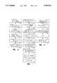
- FIG. 1is a process diagram which illustrates producing a multi-layer ceramic chip carrier (MLC) of this invention.
- MLCmulti-layer ceramic chip carrier
- FIG. 2illustrates the process for producing a fiberglass-epoxy circuit board (e.g. FR-4) of this invention.
- FIG. 3illustrates the process for producing the connections between the MLC and FR-4 in this invention.
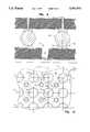
- FIG. 4is a schematic partial cross section through line 4--4 of FIG. 10 of a specific embodiment of this invention showing part of an MLC chip carrier with solder-balls attached to contacts and confronting mirror image contacts of an FR-4 circuit board.
- FIG. 5shows the positioning of solder-balls on the solder contacts prior to attachment to the MLC of FIG. 4.
- FIG. 6shows the MLC and FR-4 of FIG. 4 positioned together.
- FIG. 7shows the reflow connections of the MLC to the FR-4 of FIG. 4 in which only the joint between the solder-balls and the FR-4 is melted during reflow.
- FIG. 8illustrates the reflow connections of the MLC to the FR-4 of FIG. 4 in which both joints of each connection are simultaneously melted to provide a more symmetric connection.
- FIG. 9is a schematic cross section through line 9--9 of FIG. 10, illustrating the "dog bone” connection between plated-through-hole via connection of this invention.
- FIG. 10is a schematic plan view illustrating part of the array of metal contacts and "dog bone” connections between the plated through-holes and contacts.
- FIG. 11is larger view of the "dog-bone" arrangement of FIG. 10.
- FIG. 12is another embodiment of this invention with different sized contacts and inversely proportional solder volumes.
- FIG. 13is a plan view of a flash layer around a contact of this invention for providing sufficient solder volumes for this invention.
- FIG. 14is a cross section through line 14--14 of FIG. 13 of the contact and flash layer.
- FIG. 15schematically illustrates the information handling system of this invention.
- a first substrate 10is produced with a planer array of contacts 12 and vias 14.
- substraterefers to any component with a flat surface for interconnection which will be referred to as a major surface in contrast to a narrow edge surface.
- the inventionwill increase the reliability of connecting flexible circuit boards such as TAB-BGA (tape automated bonding ball grid array) previously known as ATAB components
- the first substrateis a rigid component such as an FR-4 or plastic chip carrier, and more preferably a ceramic or MLC (multi-layer ceramic) chip carrier for which these inventions of this application are especially well suited.
- step 101in the manufacture of ceramic chip carriers, ceramic powders are mixed with binders, solvents and plasticizer and cast to form green sheets of dielectric layers.
- step 102vias are made preferably by punching and in step 103, conductive ink or paste (e.g. Mo frit and solvent) is screened to fill the vias.
- the wiring patternmay also be screened on the surface at this time and/or exterior wiring layers may be made later using a thin film process.
- step 104green sheets are stacked and laminated with heat and pressure into a monolithic structure. Then the green sheet(s) are sintered, in step 105, by firing in an oven with a reducing atmosphere.
- a thin film processmay be used to produce an exterior wiring layer (not shown).
- conductive metalmay be evaporated or sputtered onto the substrate followed by photo-lithographic patterning which may be followed by dialectic coating and additional thin film layering.
- the contacts 12may be square or more preferably are approximately round to match the shape of the ball and to allow a closer spacing sufficient to reliably prevent solder bridging.
- the contactsmay be made from any conductive substance, preferably a metal such as Al or Ti and more preferably are made from or covered with Cu, Ni, Au, Pd, or alloys of these.
- the materialmay be deposited by screening or a photo-lithographic process may be followed by chemical and/or electric deposition processes.
- the contacts 12are covered with a volume of a first joining-material 16, such as a conductive thermoplastic or a solder alloy containing Sn, Pb, Bi, In, Ag to form solder contacts or solder bumps of LMT material.
- a first joining-material 16such as a conductive thermoplastic or a solder alloy containing Sn, Pb, Bi, In, Ag to form solder contacts or solder bumps of LMT material.
- the joining-materialis Pb/Sn based solder with 20% to 75% Sn and the balance mostly Pb and most preferably is about eutectic 63% Sn and 37% Pb.
- the LMT soldermay be deposited in the molten state by a mass soldering method such as wave soldering or may be screened as solder paste (metal particles in a organic carrier) or may be electrically and/or chemically deposited on the contacts following a photo-lithographic process.
- step 107metal-balls are attached to the solder bumps preferably by applying a layer of sticky flux 20 on which the balls are positioned.
- the ballsmay be placed simultaneously by transfer from a vacuum die.
- the fluxmay be applied just on the contacts or on the entire area of the substrate interconnections.
- the balls 18may be copper preferably coated to prevent oxidation, or more preferably are a HMT solder alloy with a melting temperature substantially higher than that of the joining-material so that the balls may be reflow joined to the contacts in step 108 without melting the balls.
- the ballsare Sn and 80% to 97% Pb, and most preferably 90%-95% Pb.
- the attachmentis made reliable by reflow heating to join the ball to the contact so the ball will not fall off during later processing.
- surface tension of the melted joining-materialwill move the balls 18 from positions shown in FIG. 5 into precise alignment with contacts 12 as shown in FIG. 4. Centering the balls on the pads of the first substrate helps align the balls with the pads 17 of the second substrate 11.
- step 109the substrate is cooled to solidify the joining-material.
- a second substrate 11is produced which also has vias 15 and a planer array of contacts 17.
- the array of contacts 17is approximately a mirror image of the array of contacts 12.
- the second substratemay be a flexible circuit board (e.g. thin polyimide and copper layers), or more preferably a rigid board such as ceramic and is most preferably a multi-layer FR-4 printed circuit board.
- FIG. 2illustrates the process of manufacturing fiberglass-epoxy circuit boards (e.g. FR-4).
- step 120one or more layers of fiberglass cloth are impregnated with epoxy resin solution to form a dielectric layer.
- the layersare only partially cured to form stable B-stage layers.
- step 121at least the internal layers are circuitized.
- FIGS. 9-13illustrate the surface wiring of this invention and is discussed in more detail later.
- This stepincludes forming a rectangular array of preferably round contacts, and forming lands for connection to the vias at the centers of squares defined by four surrounding contacts, and forming connections between the lands and contacts.
- the B-stage layersare laminated in step 122 with heat and pressure to fuse the layers and fully cure the boards.
- Each layeris circuitized by screening or by a photolithographic process in which a metal foil covering is subtractively removed or metal is chemically and/or electrically added selectively to form a wiring layer on the surface of the dielectric layer.
- step 123holes are drilled at the lands, through one or more layers, and in step 124, the holes are internally plated with metal (preferably copper) to form vias for electrical interconnection between the wiring layers on each side of the dielectric layers.
- step 125joining-material 13 (FIG. 4) is deposited on contacts 17 in a similar manner as previously described for step 106 in the process of producing MLC.
- step 131substrates 10, 11 are moved into confronting position as shown in FIG. 4, and in step 132, are brought together as shown in FIG. 6.
- the accuracy of the placement machineis limited so that the substrates are not precisely aligned.
- FIG. 7shows the results of reflow of only joining-material 13 which moves substrate 10 in the direction of arrow 40 relative to substrate 11 to precisely align the substrates.
- the connectionssuch as on either side of ball 42, are not symmetric due to tolerances in the positions of the contacts. Therefore, in step 133, as shown in FIG. 8, preferably both joining-materials 13 and 16 on either side of the solder-balls 18 are simultaneously reflowed to produce more symmetric connections.
- both joints 51 and 52are simultaneously melted the surface tension of the joining-material will move the ball in the plane 53 of the balls toward a position halfway between the centers 54, 55 of the contacts resulting in a more symmetric connection.
- Such symmetric connectionshave a greater fatigue life than the non-symmetric connections of FIG. 7.
- step 134the substrates are cooled to solidify the joining-material of the connections.
- step 135the area between the first and second substrates around the metal-balls is filled with an encapsulant such as epoxy. It is critical to the solder connection configuration invention of applicant that the connections not be encapsulated until after simultaneous reflow of the top and bottom solder joints so that the solder-balls can move into alignment between the contacts. After such alignment encapsulating the area between the substrates, around the balls, further reduces fatigue stress during thermal cycling.
- joining-material 16may initially have a lead content reduced below eutectic amounts so that during the first reflow it becomes a eutectic mixture and then the simultaneous melting during the second reflow is achieved at minimum temperatures.
- the balls in FIGS. 4-8are as large as possible to minimize fatigue stress in the connections only limited by the requirement of reliably preventing bridging between the balls. Stresses in the joints on either side of the balls would be minimized by making the contacts the same size as the balls. However, to reliably prevent bridging between the contacts, the contacts have to be significantly smaller than the balls. As shown in FIG. 8, preferably a solder mask material 58, 59 which repels liquid solder is placed between the contacts to reduce solder bridging so the contacts may be made as close to the size of the balls as possible. For example, connections with 0.9 mm nominal diameter balls and round contacts of 0.7 mm nominal diameter normally spaced at 1.25 mm centers may be made reliably without bridging.
- Solder mask materialsare well known in the art.
- volumes of LMT joining materialshould be as large as possible to reduce fatigue, but are limited by the requirements of reliably preventing bridging and of the cost or difficulty in depositing large volumes of solder.
- the minimum joint diameteris at least 2/3 of the diameter of the ball 66.
- the jointshould be at least 0.6 mm in diameter in plane 62 and more preferably larger.
- through-hole viasare usually filled with a HMT metal
- viasare usually filled or are slightly depressed in relation with contacts that are not on vias.
- wiring layersusually contain round lands of metal through which the via holes are formed and which are interconnected between wiring layers by plating the hole. Some of the contacts on FR-4 or flexible substrates may occur on such plated vias. Since the diameter of the solder joint is critical, the volume of solder is critical, but the volume can not easily be controlled at such holes (even if previously filled with LMT solder).
- FIG. 10schematically shows an arrangement of plated through hole vias 71 each connected to a solder contact 72.
- This "dog bone” arrangementprevents the solder on contact 72 from flowing into the through-hole 73.
- the centers of the contactsare approximately located at the intersections of multiple, equally spaced, parallel lines 74 and multiple, equally spaced, parallel lines 75 which are perpendicular to lines 74.
- Vias 71are located at the centers of squares 76 defined by four contacts 72 around via hole 73. The vias are connected to the contacts through a wire 77 extending under a layer of solder mask 78.
- FIG. 11schematically illustrates a single "dog bone” 80 of this invention prior to depositing joining-material on contact 82.
- a hole 81(hidden) is made by mechanical or laser drilling from the surface wiring layer into the substrate, at least to another wiring layer, and metal is deposited to form contact 82, land 83, connecting wire 84 and to plate the interior of hole 85 leaving opening 86.
- Solder mask 87covers most of connecting wire 84 and the outer edge of land 83 as indicated by dashed lines to prevent solder bridging.
- FIG. 12schematically illustrates an alternative embodiment in which metal contact 91 is larger than metal contact 92.
- a higher volume of joining-material 93is placed between ball 94 and the smaller contact 92, than the volume of solder material 95 between the solder-ball and larger contact 91.
- the minimum cross sections of the joints on each side of the solder-ballmay be made about equal to equalize fatigue at each joint of the connection.
- FIGS. 13 and 14illustrate a technique to provide higher levels of solder deposited on a contact than can usually be deposited by wave soldering, electrical, or chemical (electroless) deposition.
- Flash layer 130extends out from contact pad 132 over the layer of solder resist 134 the thickness of the flash is exaggerated for illustration.
- Solder 136is deposited electrically, chemically, or preferably by melted solder wave.
- the flashis a conductive substance for electrical deposition, or seed materials such as palladium for electroless plating, a solder wettable material for wave soldering.
- the thickness of the flash materialis selected to completely dissolve the flash during reflow, resulting in all the solder migrating onto contact pad 132.
- the flashis copper or tin which is sufficiently thick to survive during deposition, but thin enough to fully dissolve during reflow.
- the thickness of the solder deposited by molten solder wavegenerally increases as the size of the flash area increases.
- FIG. 15shows an information handling system 150 in which computer assembly 151 includes central processor module 152 communicating through one or more wiring layers e.g. a bus 160 in substrate 153 with computer memory module 154 (e.g. RAM).
- Computer 151communicates with computer 155 through cable 156. Additional connections (not shown) for cables may be provided for I/O with computer peripherals.
- Computer 155also includes central processor module 157 communicating through one or more wiring layers (bus 161) in substrate 158 with computer memory module 159.
- One or preferably both modules of each computerare connected to the substrate using the preferred solder-ball or solder column connections of the invention.
- FIG. 16illustrates solder columns 160 which are similar to the solder-balls 18 (FIG. 4) and the previous discussion on materials, geometries, and methods of placement, reflow joining to the modules, reflow connection to the substrates are applicable.
- the columnshave approximately hemispherical ends and are preferably from 1 to 20 times longer then their diameters. Fatigue is reduced by making the columns longer, but longer columns result in higher module profiles, reduced lead cooling, and handling problems that militate against the length exceeding that necessary to reliably prevent thermal fatigue failures.
- solder-ballincludes hemispherical ended solder columns. In order to join the columns to the module, columns may be reflow heated while attached to the bottom side of the module (i.e. inverted position). This results in the columns being closely centered on the contacts and vertically aligned very accurately.
- Vacuum die 172includes a flat face 173 with recesses which fit the solder-ball or solder column.
- the recesses 174communicate with a vacuum reservoir 175 through passages 176 which are significantly smaller than the solder balls or columns to reliably prevent the columns from entering vacuum reservoir 175 and to prevent jamming.
- the vacuum dieis used to position the balls or columns on the contacts of substrate 178 either as shown in FIG. 17 or in an inverted position. Either round or square end columns can be reflow joined in inverted position as in FIG. 16 or by holding the columns vertical during reflow preferably using the vacuum die. The vacuum can be turned off or even reversed during reflow allowing the columns to rest against the solder contacts.
Landscapes
- Engineering & Computer Science (AREA)
- Microelectronics & Electronic Packaging (AREA)
- Physics & Mathematics (AREA)
- Condensed Matter Physics & Semiconductors (AREA)
- General Physics & Mathematics (AREA)
- Computer Hardware Design (AREA)
- Power Engineering (AREA)
- Manufacturing & Machinery (AREA)
- Ceramic Engineering (AREA)
- Mechanical Engineering (AREA)
- Geometry (AREA)
- Combinations Of Printed Boards (AREA)
- Electric Connection Of Electric Components To Printed Circuits (AREA)
- Manufacturing Of Printed Wiring (AREA)
- Pens And Brushes (AREA)
- Manufacturing Of Electrical Connectors (AREA)
- Piezo-Electric Or Mechanical Vibrators, Or Delay Or Filter Circuits (AREA)
Abstract
Description
Claims (28)
Priority Applications (16)
| Application Number | Priority Date | Filing Date | Title |
|---|---|---|---|
| US08/144,981US5591941A (en) | 1993-10-28 | 1993-10-28 | Solder ball interconnected assembly |
| EP99125770AEP1002611A1 (en) | 1993-10-28 | 1994-09-16 | Solder ball connections and assembly process |
| AT94114605TATE231042T1 (en) | 1993-10-28 | 1994-09-16 | PROVIDED WITH SOLDER BALLS CONNECTION METHOD |
| EP99125769AEP1002610A1 (en) | 1993-10-28 | 1994-09-16 | Solder ball connections and assembly process |
| AT99125772TATE283136T1 (en) | 1993-10-28 | 1994-09-16 | PROVIDED WITH SOLDER BALLS CONNECTION METHOD |
| EP94114605AEP0650795B1 (en) | 1993-10-28 | 1994-09-16 | Solder ball connections and assembly process |
| EP99125772AEP1008414B1 (en) | 1993-10-28 | 1994-09-16 | Solder ball connections and assembly process |
| DE69434160TDE69434160T2 (en) | 1993-10-28 | 1994-09-16 | Provided with solder balls connecting method so |
| DE69432010TDE69432010T2 (en) | 1993-10-28 | 1994-09-16 | Provide it with soldering balls |
| KR1019940026699AKR0167808B1 (en) | 1993-10-28 | 1994-10-19 | Interconnect structure and method for manufacturing same and information processing device |
| CA002134019ACA2134019C (en) | 1993-10-28 | 1994-10-21 | Solder ball connections and assembly process |
| BR9404248ABR9404248A (en) | 1993-10-28 | 1994-10-26 | Set of interconnections by welding spheres, assembly and reproduction processes, system and apparatus that encompasses them |
| JP6264279AJP2500109B2 (en) | 1993-10-28 | 1994-10-27 | Substrate interconnection method and connection structure thereof |
| TW083111621ATW261556B (en) | 1993-10-28 | 1994-12-13 | |
| US08/474,343US5675889A (en) | 1993-10-28 | 1995-06-07 | Solder ball connections and assembly process |
| US08/640,645US6504105B1 (en) | 1993-10-28 | 1996-05-01 | Solder ball connections and assembly process |
Applications Claiming Priority (1)
| Application Number | Priority Date | Filing Date | Title |
|---|---|---|---|
| US08/144,981US5591941A (en) | 1993-10-28 | 1993-10-28 | Solder ball interconnected assembly |
Related Child Applications (2)
| Application Number | Title | Priority Date | Filing Date |
|---|---|---|---|
| US08/474,343DivisionUS5675889A (en) | 1993-10-28 | 1995-06-07 | Solder ball connections and assembly process |
| US08/640,645ContinuationUS6504105B1 (en) | 1993-10-28 | 1996-05-01 | Solder ball connections and assembly process |
Publications (1)
| Publication Number | Publication Date |
|---|---|
| US5591941Atrue US5591941A (en) | 1997-01-07 |
Family
ID=22511057
Family Applications (3)
| Application Number | Title | Priority Date | Filing Date |
|---|---|---|---|
| US08/144,981Expired - LifetimeUS5591941A (en) | 1993-10-28 | 1993-10-28 | Solder ball interconnected assembly |
| US08/474,343Expired - LifetimeUS5675889A (en) | 1993-10-28 | 1995-06-07 | Solder ball connections and assembly process |
| US08/640,645Expired - LifetimeUS6504105B1 (en) | 1993-10-28 | 1996-05-01 | Solder ball connections and assembly process |
Family Applications After (2)
| Application Number | Title | Priority Date | Filing Date |
|---|---|---|---|
| US08/474,343Expired - LifetimeUS5675889A (en) | 1993-10-28 | 1995-06-07 | Solder ball connections and assembly process |
| US08/640,645Expired - LifetimeUS6504105B1 (en) | 1993-10-28 | 1996-05-01 | Solder ball connections and assembly process |
Country Status (9)
| Country | Link |
|---|---|
| US (3) | US5591941A (en) |
| EP (4) | EP1002611A1 (en) |
| JP (1) | JP2500109B2 (en) |
| KR (1) | KR0167808B1 (en) |
| AT (2) | ATE231042T1 (en) |
| BR (1) | BR9404248A (en) |
| CA (1) | CA2134019C (en) |
| DE (2) | DE69432010T2 (en) |
| TW (1) | TW261556B (en) |
Cited By (94)
| Publication number | Priority date | Publication date | Assignee | Title |
|---|---|---|---|---|
| US5729438A (en)* | 1996-06-07 | 1998-03-17 | Motorola, Inc. | Discrete component pad array carrier |
| US5734199A (en)* | 1995-12-18 | 1998-03-31 | Matsushita Electric Industrial Co., Ltd. | Semiconductor device having improved test electrodes |
| US5796038A (en)* | 1997-06-16 | 1998-08-18 | Vlsi Technology, Inc. | Technique to produce cavity-up HBGA packages |
| US5847456A (en)* | 1996-02-28 | 1998-12-08 | Nec Corporation | Semiconductor device |
| US5872400A (en)* | 1997-06-25 | 1999-02-16 | International Business Machines Corporation | High melting point solder ball coated with a low melting point solder |
| US5875102A (en)* | 1995-12-20 | 1999-02-23 | Intel Corporation | Eclipse via in pad structure |
| US5876219A (en)* | 1997-08-29 | 1999-03-02 | The Whitaker Corp. | Board-to-board connector assembly |
| US5912505A (en)* | 1995-11-07 | 1999-06-15 | Sumitomo Metal (Smi) Electronics Devices, Inc. | Semiconductor package and semiconductor device |
| US5936848A (en)* | 1995-12-20 | 1999-08-10 | Intel Corporation | Electronics package that has a substrate with an array of hollow vias and solder balls that are eccentrically located on the vias |
| US5997317A (en)* | 1998-09-29 | 1999-12-07 | Hon Hai Precision Ind. Co., Ltd. | Ball grid array connector |
| US6016005A (en)* | 1998-02-09 | 2000-01-18 | Cellarosi; Mario J. | Multilayer, high density micro circuit module and method of manufacturing same |
| US6020561A (en)* | 1996-03-29 | 2000-02-01 | Intel Corporation | Printed circuit substrate with solder formed on pad-on-via and pad-off-via contacts thereof |
| US6024584A (en)* | 1996-10-10 | 2000-02-15 | Berg Technology, Inc. | High density connector |
| US6040618A (en)* | 1997-03-06 | 2000-03-21 | Micron Technology, Inc. | Multi-chip module employing a carrier substrate with micromachined alignment structures and method of forming |
| US6043559A (en)* | 1996-09-09 | 2000-03-28 | Intel Corporation | Integrated circuit package which contains two in plane voltage busses and a wrap around conductive strip that connects a bond finger to one of the busses |
| US6043985A (en)* | 1996-11-11 | 2000-03-28 | Fraunhofer-Gesellschaft Zur Forderung Der Angewandten Forschung E.V. | Thermal connecting structure for connecting materials with different expansion coefficients |
| US6043990A (en)* | 1997-06-09 | 2000-03-28 | Prototype Solutions Corporation | Multiple board package employing solder balis and fabrication method and apparatus |
| US6076726A (en)* | 1998-07-01 | 2000-06-20 | International Business Machines Corporation | Pad-on-via assembly technique |
| US6093035A (en)* | 1996-06-28 | 2000-07-25 | Berg Technology, Inc. | Contact for use in an electrical connector |
| US6116923A (en)* | 1998-12-18 | 2000-09-12 | Hon Hai Precision Ind. Co., Ltd. | Electrical connector |
| US6132543A (en)* | 1997-03-14 | 2000-10-17 | Matsushita Electric Industrial Co., Ltd. | Method of manufacturing a packaging substrate |
| US6137693A (en)* | 1998-07-31 | 2000-10-24 | Agilent Technologies Inc. | High-frequency electronic package with arbitrarily-shaped interconnects and integral shielding |
| US6139336A (en)* | 1996-11-14 | 2000-10-31 | Berg Technology, Inc. | High density connector having a ball type of contact surface |
| US6146203A (en)* | 1995-06-12 | 2000-11-14 | Berg Technology, Inc. | Low cross talk and impedance controlled electrical connector |
| US6198634B1 (en)* | 1999-03-31 | 2001-03-06 | International Business Machines Corporation | Electronic package with stacked connections |
| US6199741B1 (en)* | 1998-12-09 | 2001-03-13 | International Business Machines Corporation | Enhanced pad design for substrate |
| US6235996B1 (en)* | 1998-01-28 | 2001-05-22 | International Business Machines Corporation | Interconnection structure and process module assembly and rework |
| US6252779B1 (en) | 1999-01-25 | 2001-06-26 | International Business Machines Corporation | Ball grid array via structure |
| US6278180B1 (en)* | 1997-06-04 | 2001-08-21 | Nikko Company | Ball-grid-array-type semiconductor device and its fabrication method and electronic device |
| US6297559B1 (en)* | 1997-07-10 | 2001-10-02 | International Business Machines Corporation | Structure, materials, and applications of ball grid array interconnections |
| US6300164B1 (en) | 1997-07-10 | 2001-10-09 | International Business Machines Corporation | Structure, materials, and methods for socketable ball grid |
| US6307160B1 (en)* | 1998-10-29 | 2001-10-23 | Agilent Technologies, Inc. | High-strength solder interconnect for copper/electroless nickel/immersion gold metallization solder pad and method |
| US6325644B1 (en) | 1996-10-10 | 2001-12-04 | Berg Technology, Inc. | High density connector and method of manufacture |
| US6330967B1 (en)* | 1997-03-13 | 2001-12-18 | International Business Machines Corporation | Process to produce a high temperature interconnection |
| US6337522B1 (en)* | 1997-07-10 | 2002-01-08 | International Business Machines Corporation | Structure employing electrically conductive adhesives |
| US6340113B1 (en) | 1995-10-06 | 2002-01-22 | Donald H. Avery | Soldering methods and compositions |
| US6350669B1 (en) | 2000-10-30 | 2002-02-26 | Siliconware Precision Industries Co., Ltd. | Method of bonding ball grid array package to circuit board without causing package collapse |
| US20020050404A1 (en)* | 1994-07-20 | 2002-05-02 | Toshiya Akamatsu | Integrated electronic device having flip-chip connection with circuit board and fabrication method thereof |
| US6394819B1 (en) | 1998-10-29 | 2002-05-28 | The Whitaker Corporation | Dielectric member for absorbing thermal expansion and contraction at electrical interfaces |
| US20020084105A1 (en)* | 2000-12-29 | 2002-07-04 | Phil Geng | Via -in-pad with off-center geometry and methods of manufacture |
| US6495916B1 (en)* | 1999-04-06 | 2002-12-17 | Oki Electric Industry Co., Ltd. | Resin-encapsulated semiconductor device |
| US20030011098A1 (en)* | 2000-05-31 | 2003-01-16 | Lewis Charles W. | PCB support plate method for PCB via fill |
| US20030040166A1 (en)* | 2001-05-25 | 2003-02-27 | Mark Moshayedi | Apparatus and method for stacking integrated circuits |
| US6531232B1 (en)* | 1998-10-29 | 2003-03-11 | Commissariat A L'energie Atomique | System for assembling substrates to bonding zones provided with cavities |
| US6533159B1 (en) | 1998-10-07 | 2003-03-18 | Micron Technology, Inc. | Apparatus for attaching solder balls to BGA package utilizing a tool to pick and dip the solder ball in flux |
| US20030067082A1 (en)* | 2001-05-25 | 2003-04-10 | Mark Moshayedi | Apparatus and methods for stacking integrated circuit devices with interconnected stacking structure |
| US20030080406A1 (en)* | 2001-10-30 | 2003-05-01 | Krishna Seshan | Power gridding scheme |
| US6574861B1 (en) | 2001-04-11 | 2003-06-10 | Applied Micro Circuits Corporation | System and method for solder ball rework |
| US6739879B2 (en)* | 2002-07-03 | 2004-05-25 | Intel Corporation | Ball grid array circuit board jumper |
| US6762487B2 (en) | 2001-04-19 | 2004-07-13 | Simpletech, Inc. | Stack arrangements of chips and interconnecting members |
| US20040256737A1 (en)* | 2003-06-20 | 2004-12-23 | Min-Lung Huang | [flip-chip package substrate and flip-chip bonding process thereof] |
| US20040257096A1 (en)* | 2003-06-17 | 2004-12-23 | Johnson Kenneth William | Back side probing method and assembly |
| US20050098338A1 (en)* | 1999-12-27 | 2005-05-12 | Matsushita Electric Industrial Co., Ltd. | Electronic part, and electronic part mounting element and an process for manufacturing such the articles |
| US20050104210A1 (en)* | 1996-05-21 | 2005-05-19 | Farnworth Warren M. | Use of palladium in IC manufacturing with conductive polymer bump |
| US20050128721A1 (en)* | 2003-12-16 | 2005-06-16 | Tay Cheng S. | Printed circuit boards having pads for solder balls and methods for the implementation thereof |
| US20050173795A1 (en)* | 2004-02-05 | 2005-08-11 | Hodson Kenneth G. | Socket grid array |
| US20050189627A1 (en)* | 2004-02-27 | 2005-09-01 | Fujio Ito | Method of surface mounting a semiconductor device |
| US6939173B1 (en) | 1995-06-12 | 2005-09-06 | Fci Americas Technology, Inc. | Low cross talk and impedance controlled electrical connector with solder masses |
| US20050221675A1 (en)* | 2003-07-16 | 2005-10-06 | Rathburn James J | Fine pitch electrical interconnect assembly |
| US20060000641A1 (en)* | 2004-06-30 | 2006-01-05 | Salama Islam A | Laser metallization for ceramic device |
| US20060035483A1 (en)* | 2003-07-16 | 2006-02-16 | Gryphics, Inc. | Fine pitch electrical interconnect assembly |
| US7032306B1 (en) | 1999-02-05 | 2006-04-25 | Societe Novatec S.A. | Method for producing module |
| US7078820B2 (en)* | 1998-09-01 | 2006-07-18 | Sony Corporation | Semiconductor apparatus and process of production thereof |
| US20070117268A1 (en)* | 2005-11-23 | 2007-05-24 | Baker Hughes, Inc. | Ball grid attachment |
| US20070278654A1 (en)* | 2001-01-16 | 2007-12-06 | Jimarez Lisa J | Method of making an electronic package |
| US20080099890A1 (en)* | 2006-10-30 | 2008-05-01 | Powertech Technology Inc. | Ball grid array package structure |
| US20080182436A1 (en)* | 2003-07-16 | 2008-07-31 | Gryphics, Inc. | Fine pitch electrical interconnect assembly |
| US20080202804A1 (en)* | 2007-02-26 | 2008-08-28 | Yasuhiro Fakutomi | Printed circuit board and method of producing the same |
| US20090134207A1 (en)* | 2007-11-28 | 2009-05-28 | Eu Poh Leng | Solder ball attachment ring and method of use |
| US20100018763A1 (en)* | 2008-07-24 | 2010-01-28 | Gm Global Technology Operations, Inc. | Printed circuit board ball grid array system having improved mechanical strength |
| US20100326726A1 (en)* | 2009-06-24 | 2010-12-30 | Fujitsu Limited | Solder joint structure, electronic device using the same, and solder bonding method |
| US20110019379A1 (en)* | 2009-07-22 | 2011-01-27 | Nec Electronics Corporation | Printed wiring board, semiconductor device, and method for manufacturing printed wiring board |
| US8044502B2 (en) | 2006-03-20 | 2011-10-25 | Gryphics, Inc. | Composite contact for fine pitch electrical interconnect assembly |
| US20120161312A1 (en)* | 2010-12-23 | 2012-06-28 | Hossain Md Altaf | Non-solder metal bumps to reduce package height |
| US20120241876A1 (en)* | 2011-03-25 | 2012-09-27 | Still Charles A | System and method for improving frequency response |
| USD718253S1 (en) | 2012-04-13 | 2014-11-25 | Fci Americas Technology Llc | Electrical cable connector |
| US20140355228A1 (en)* | 2013-05-29 | 2014-12-04 | Finisar Corporation | Rigid-flexible circuit interconnects |
| US8905651B2 (en) | 2012-01-31 | 2014-12-09 | Fci | Dismountable optical coupling device |
| USD720698S1 (en) | 2013-03-15 | 2015-01-06 | Fci Americas Technology Llc | Electrical cable connector |
| US8944831B2 (en) | 2012-04-13 | 2015-02-03 | Fci Americas Technology Llc | Electrical connector having ribbed ground plate with engagement members |
| USD727268S1 (en) | 2012-04-13 | 2015-04-21 | Fci Americas Technology Llc | Vertical electrical connector |
| USD727852S1 (en) | 2012-04-13 | 2015-04-28 | Fci Americas Technology Llc | Ground shield for a right angle electrical connector |
| US9048583B2 (en) | 2009-03-19 | 2015-06-02 | Fci Americas Technology Llc | Electrical connector having ribbed ground plate |
| USD733662S1 (en) | 2013-01-25 | 2015-07-07 | Fci Americas Technology Llc | Connector housing for electrical connector |
| USD746236S1 (en) | 2012-07-11 | 2015-12-29 | Fci Americas Technology Llc | Electrical connector housing |
| US9257778B2 (en) | 2012-04-13 | 2016-02-09 | Fci Americas Technology | High speed electrical connector |
| US9543703B2 (en) | 2012-07-11 | 2017-01-10 | Fci Americas Technology Llc | Electrical connector with reduced stack height |
| US20170110392A1 (en)* | 2015-10-15 | 2017-04-20 | Advanced Semiconductor Engineering, Inc. | Semiconductor package structure and method for manufacturing the same structure |
| US20170271291A1 (en)* | 2012-08-17 | 2017-09-21 | Taiwan Semiconductor Manufacturing Company, Ltd. | Bonded Structures for Package and Substrate |
| US20170287862A1 (en)* | 2014-09-09 | 2017-10-05 | Senju Metal Industry Co., Ltd. | Cu Column, Cu Core Column, Solder Joint, and Through-Silicon Via |
| US20180005976A1 (en)* | 2013-07-17 | 2018-01-04 | Taiwan Semiconductor Manufacturing Company, Ltd. | Mechanisms For Forming Bonding Structures |
| US20180020554A1 (en)* | 2012-03-20 | 2018-01-18 | Alpha Assembly Solutions Inc. | Solder Preforms and Solder Alloy Assembly Methods |
| US10163839B2 (en) | 2012-07-31 | 2018-12-25 | Taiwan Semiconductor Manufacturing Company, Ltd. | Bump on pad (BOP) bonding structure in semiconductor packaged device |
| US12127334B2 (en) | 2019-02-01 | 2024-10-22 | Dis Tech America, Llc | Maintaining the shape of a circuit board |
Families Citing this family (68)
| Publication number | Priority date | Publication date | Assignee | Title |
|---|---|---|---|---|
| GB9510085D0 (en)* | 1995-05-18 | 1995-07-12 | Sherritt Inc | A connective medium and a process for connecting electronic devices to circuit boards |
| WO1997023121A1 (en)* | 1995-12-19 | 1997-06-26 | Thermicedge Corporation | Spheres useful in a detachable connective medium for ball grid array assemblies |
| US6404063B2 (en) | 1995-12-22 | 2002-06-11 | Micron Technology, Inc. | Die-to-insert permanent connection and method of forming |
| US5686318A (en)* | 1995-12-22 | 1997-11-11 | Micron Technology, Inc. | Method of forming a die-to-insert permanent connection |
| US6000126A (en)* | 1996-03-29 | 1999-12-14 | General Dynamics Information Systems, Inc. | Method and apparatus for connecting area grid arrays to printed wire board |
| US6395991B1 (en)* | 1996-07-29 | 2002-05-28 | International Business Machines Corporation | Column grid array substrate attachment with heat sink stress relief |
| US6083768A (en)* | 1996-09-06 | 2000-07-04 | Micron Technology, Inc. | Gravitationally-assisted control of spread of viscous material applied to semiconductor assembly components |
| US5897335A (en)* | 1997-02-04 | 1999-04-27 | Integrated Device Technology, Inc. | Flip-chip bonding method |
| US6059172A (en)* | 1997-06-25 | 2000-05-09 | International Business Machines Corporation | Method for establishing electrical communication between a first object having a solder ball and a second object |
| US5953816A (en)* | 1997-07-16 | 1999-09-21 | General Dynamics Information Systems, Inc. | Process of making interposers for land grip arrays |
| US6372624B1 (en)* | 1997-08-04 | 2002-04-16 | Micron Technology, Inc. | Method for fabricating solder bumps by wave soldering |
| US6107122A (en)* | 1997-08-04 | 2000-08-22 | Micron Technology, Inc. | Direct die contact (DDC) semiconductor package |
| TW362342B (en)* | 1997-10-27 | 1999-06-21 | Sony Video Taiwan Co Ltd | Method for combining e-mail network with pager |
| US6369451B2 (en)* | 1998-01-13 | 2002-04-09 | Paul T. Lin | Solder balls and columns with stratified underfills on substrate for flip chip joining |
| US6268275B1 (en)* | 1998-10-08 | 2001-07-31 | Micron Technology, Inc. | Method of locating conductive spheres utilizing screen and hopper of solder balls |
| US6285083B1 (en)* | 1999-03-24 | 2001-09-04 | Shinko Electric Industries Co., Ltd. | Semiconductor device and mounting structure of a semiconductor device |
| US6177729B1 (en) | 1999-04-03 | 2001-01-23 | International Business Machines Corporation | Rolling ball connector |
| US6675469B1 (en)* | 1999-08-11 | 2004-01-13 | Tessera, Inc. | Vapor phase connection techniques |
| US6741778B1 (en) | 2000-05-23 | 2004-05-25 | International Business Machines Corporation | Optical device with chip level precision alignment |
| JP2002153990A (en)* | 2000-11-21 | 2002-05-28 | Senju Metal Ind Co Ltd | Alloy for solder ball |
| US6377475B1 (en) | 2001-02-26 | 2002-04-23 | Gore Enterprise Holdings, Inc. | Removable electromagnetic interference shield |
| US6475558B2 (en) | 2001-02-26 | 2002-11-05 | Volvo Trucks North America, Inc. | Vehicle electrical ground and process |
| TW519310U (en)* | 2001-12-18 | 2003-01-21 | Via Tech Inc | Electric connection apparatus |
| US6744640B2 (en) | 2002-04-10 | 2004-06-01 | Gore Enterprise Holdings, Inc. | Board-level EMI shield with enhanced thermal dissipation |
| JP3819806B2 (en)* | 2002-05-17 | 2006-09-13 | 富士通株式会社 | Electronic component with bump electrode and manufacturing method thereof |
| US6817094B2 (en)* | 2002-11-13 | 2004-11-16 | Ted Ju | Method of making an electrical connector |
| US8403203B2 (en)* | 2002-12-10 | 2013-03-26 | Neonoda Inc. | Component bonding using a capillary effect |
| US6906598B2 (en) | 2002-12-31 | 2005-06-14 | Mcnc | Three dimensional multimode and optical coupling devices |
| TW200414858A (en)* | 2003-01-15 | 2004-08-01 | Senju Metal Industry Co | Apparatus and method for aligning and attaching solder columns to a substrate |
| JP2005026364A (en)* | 2003-06-30 | 2005-01-27 | Sanyo Electric Co Ltd | Hybrid integrated circuit |
| US20050003650A1 (en)* | 2003-07-02 | 2005-01-06 | Shriram Ramanathan | Three-dimensional stacked substrate arrangements |
| US20050045697A1 (en) | 2003-08-26 | 2005-03-03 | Lacap Efren M. | Wafer-level chip scale package |
| US7416106B1 (en)* | 2003-09-29 | 2008-08-26 | Emc Corporation | Techniques for creating optimized pad geometries for soldering |
| US6845279B1 (en) | 2004-02-06 | 2005-01-18 | Integrated Technologies, Inc. | Error proofing system for portable tools |
| US7095105B2 (en)* | 2004-03-23 | 2006-08-22 | Texas Instruments Incorporated | Vertically stacked semiconductor device |
| JP4625674B2 (en)* | 2004-10-15 | 2011-02-02 | 株式会社東芝 | Printed wiring board and information processing apparatus mounting this board |
| US7523852B2 (en)* | 2004-12-05 | 2009-04-28 | International Business Machines Corporation | Solder interconnect structure and method using injection molded solder |
| JPWO2006064863A1 (en)* | 2004-12-17 | 2008-06-12 | イビデン株式会社 | Printed wiring board |
| TWI275332B (en)* | 2005-04-26 | 2007-03-01 | Phoenix Prec Technology Corp | Method for fabricating interlayer conducting structure of circuit board |
| US7422448B2 (en)* | 2005-07-28 | 2008-09-09 | Delphi Technologies, Inc. | Surface mount connector |
| US20070090170A1 (en)* | 2005-10-20 | 2007-04-26 | Endicott Interconnect Technologies, Inc. | Method of making a circuitized substrate having a plurality of solder connection sites thereon |
| US20070108619A1 (en)* | 2005-11-15 | 2007-05-17 | Hsu Jun C | Bonding pad with high bonding strength to solder ball and bump |
| US7545042B2 (en)* | 2005-12-22 | 2009-06-09 | Princo Corp. | Structure combining an IC integrated substrate and a carrier, and method of manufacturing such structure |
| US7344318B2 (en)* | 2006-03-22 | 2008-03-18 | Intel Corporation | Optical interconnect with passive optical alignment |
| JP2007287712A (en)* | 2006-04-12 | 2007-11-01 | Oki Electric Ind Co Ltd | Semiconductor device, packaging structure thereof, and manufacturing method of semiconductor device and packaging structure |
| FR2928491A1 (en)* | 2008-03-06 | 2009-09-11 | Commissariat Energie Atomique | METHOD AND DEVICE FOR MANUFACTURING AN ASSEMBLY OF AT LEAST TWO MICROELECTRONIC CHIPS |
| US8389862B2 (en) | 2008-10-07 | 2013-03-05 | Mc10, Inc. | Extremely stretchable electronics |
| US8097926B2 (en) | 2008-10-07 | 2012-01-17 | Mc10, Inc. | Systems, methods, and devices having stretchable integrated circuitry for sensing and delivering therapy |
| US8886334B2 (en)* | 2008-10-07 | 2014-11-11 | Mc10, Inc. | Systems, methods, and devices using stretchable or flexible electronics for medical applications |
| US8372726B2 (en)* | 2008-10-07 | 2013-02-12 | Mc10, Inc. | Methods and applications of non-planar imaging arrays |
| US9123614B2 (en) | 2008-10-07 | 2015-09-01 | Mc10, Inc. | Methods and applications of non-planar imaging arrays |
| JP5646492B2 (en)* | 2008-10-07 | 2014-12-24 | エムシー10 インコーポレイテッドMc10,Inc. | Stretchable integrated circuit and device with sensor array |
| WO2011041727A1 (en) | 2009-10-01 | 2011-04-07 | Mc10, Inc. | Protective cases with integrated electronics |
| US20110218756A1 (en)* | 2009-10-01 | 2011-09-08 | Mc10, Inc. | Methods and apparatus for conformal sensing of force and/or acceleration at a person's head |
| US20120069528A1 (en)* | 2010-09-17 | 2012-03-22 | Irvine Sensors Corporation | Method for Control of Solder Collapse in Stacked Microelectronic Structure |
| KR101712459B1 (en)* | 2010-11-29 | 2017-03-22 | 삼성전자 주식회사 | Method of fabricating stacked package, and method of mounting stacked package fabricated by the same |
| JP2014523633A (en) | 2011-05-27 | 2014-09-11 | エムシー10 インコーポレイテッド | Electronic, optical and / or mechanical devices and systems and methods of manufacturing these devices and systems |
| US9171794B2 (en) | 2012-10-09 | 2015-10-27 | Mc10, Inc. | Embedding thin chips in polymer |
| US9398700B2 (en)* | 2013-06-21 | 2016-07-19 | Invensas Corporation | Method of forming a reliable microelectronic assembly |
| JP5692314B2 (en)* | 2013-09-03 | 2015-04-01 | 千住金属工業株式会社 | Bump electrode, bump electrode substrate and manufacturing method thereof |
| US9355927B2 (en) | 2013-11-25 | 2016-05-31 | Taiwan Semiconductor Manufacturing Company Ltd. | Semiconductor packaging and manufacturing method thereof |
| US10157821B1 (en)* | 2017-05-30 | 2018-12-18 | Advanced Semiconductor Engineering, Inc. | Semiconductor packages |
| KR101996910B1 (en)* | 2017-10-25 | 2019-07-05 | 주식회사 코세스 | Method of stacking substrates for semiconductor device |
| CN111799358A (en)* | 2020-06-11 | 2020-10-20 | 淮安澳洋顺昌光电技术有限公司 | Preparation method of LED chip with Sn bonding pad |
| TWI811053B (en)* | 2022-08-04 | 2023-08-01 | 矽品精密工業股份有限公司 | Carrier structure |
| TWI812442B (en)* | 2022-08-31 | 2023-08-11 | 晶呈科技股份有限公司 | Via filling method of a through-glass via plate |
| KR20240139656A (en)* | 2023-03-15 | 2024-09-24 | 주식회사 프로텍 | Method of Bonding Column Type Deposits |
| CN118737836A (en)* | 2023-03-28 | 2024-10-01 | 普罗科技有限公司 | Substrate bonding method for columnar connector |
Citations (35)
| Publication number | Priority date | Publication date | Assignee | Title |
|---|---|---|---|---|
| US3401126A (en)* | 1965-06-18 | 1968-09-10 | Ibm | Method of rendering noble metal conductive composition non-wettable by solder |
| US3403438A (en)* | 1964-12-02 | 1968-10-01 | Corning Glass Works | Process for joining transistor chip to printed circuit |
| US3429040A (en)* | 1965-06-18 | 1969-02-25 | Ibm | Method of joining a component to a substrate |
| US3518756A (en)* | 1967-08-22 | 1970-07-07 | Ibm | Fabrication of multilevel ceramic,microelectronic structures |
| US3554877A (en)* | 1968-02-07 | 1971-01-12 | Us Army | Method of making printed circuit assemblies |
| US3701076A (en)* | 1969-12-18 | 1972-10-24 | Bell Telephone Labor Inc | Intercept connector having two diode mounting holes separated by a diode supporting recess |
| US3791858A (en)* | 1971-12-13 | 1974-02-12 | Ibm | Method of forming multi-layer circuit panels |
| US3988405A (en)* | 1971-04-07 | 1976-10-26 | Smith Robert D | Process for forming thin walled articles or thin sheets |
| US4132341A (en)* | 1977-01-31 | 1979-01-02 | Zenith Radio Corporation | Hybrid circuit connector assembly |
| US4202007A (en)* | 1978-06-23 | 1980-05-06 | International Business Machines Corporation | Multi-layer dielectric planar structure having an internal conductor pattern characterized with opposite terminations disposed at a common edge surface of the layers |
| EP0084464A2 (en)* | 1982-01-20 | 1983-07-27 | North American Specialities Corporation | Connector for electronic subassemblies |
| US4413309A (en)* | 1980-07-17 | 1983-11-01 | Sony Corporation | Printed circuit board |
| US4545610A (en)* | 1983-11-25 | 1985-10-08 | International Business Machines Corporation | Method for forming elongated solder connections between a semiconductor device and a supporting substrate |
| US4604644A (en)* | 1985-01-28 | 1986-08-05 | International Business Machines Corporation | Solder interconnection structure for joining semiconductor devices to substrates that have improved fatigue life, and process for making |
| GB2177641A (en)* | 1983-06-30 | 1987-01-28 | Raychem Corp | Solder preforms |
| US4681654A (en)* | 1986-05-21 | 1987-07-21 | International Business Machines Corporation | Flexible film semiconductor chip carrier |
| US4701482A (en)* | 1985-05-24 | 1987-10-20 | Shin-Etsu Chemical Co., Ltd. | Epoxy resin composition for encapsulation of semiconductor devices |
| EP0248566A2 (en)* | 1986-05-30 | 1987-12-09 | AT&T Corp. | Process for controlling solder joint geometry when surface mounting a leadless integrated circuit package on a substrate |
| EP0263222A1 (en)* | 1986-10-08 | 1988-04-13 | International Business Machines Corporation | Method of forming solder terminals for a pinless ceramic module |
| US4831724A (en)* | 1987-08-04 | 1989-05-23 | Western Digital Corporation | Apparatus and method for aligning surface mountable electronic components on printed circuit board pads |
| US4845542A (en)* | 1987-03-19 | 1989-07-04 | Unisys Corporation | Interconnect for layered integrated circuit assembly |
| US4914814A (en)* | 1989-05-04 | 1990-04-10 | International Business Machines Corporation | Process of fabricating a circuit package |
| US4999699A (en)* | 1990-03-14 | 1991-03-12 | International Business Machines Corporation | Solder interconnection structure and process for making |
| US5060844A (en)* | 1990-07-18 | 1991-10-29 | International Business Machines Corporation | Interconnection structure and test method |
| US5120678A (en)* | 1990-11-05 | 1992-06-09 | Motorola Inc. | Electrical component package comprising polymer-reinforced solder bump interconnection |
| US5133495A (en)* | 1991-08-12 | 1992-07-28 | International Business Machines Corporation | Method of bonding flexible circuit to circuitized substrate to provide electrical connection therebetween |
| US5147084A (en)* | 1990-07-18 | 1992-09-15 | International Business Machines Corporation | Interconnection structure and test method |
| US5159535A (en)* | 1987-03-11 | 1992-10-27 | International Business Machines Corporation | Method and apparatus for mounting a flexible film semiconductor chip carrier on a circuitized substrate |
| US5201451A (en)* | 1987-03-11 | 1993-04-13 | International Business Machines Corp. | Method and apparatus for mounting a flexible film semiconductor chip carrier on a circuitized substrate |
| US5203075A (en)* | 1991-08-12 | 1993-04-20 | Inernational Business Machines | Method of bonding flexible circuit to cicuitized substrate to provide electrical connection therebetween using different solders |
| US5241133A (en)* | 1990-12-21 | 1993-08-31 | Motorola, Inc. | Leadless pad array chip carrier |
| US5261155A (en)* | 1991-08-12 | 1993-11-16 | International Business Machines Corporation | Method for bonding flexible circuit to circuitized substrate to provide electrical connection therebetween using different solders |
| US5371328A (en)* | 1993-08-20 | 1994-12-06 | International Business Machines Corporation | Component rework |
| US5379189A (en)* | 1992-11-03 | 1995-01-03 | Smiths Industries Limited Company | Electrical assemblies |
| US5386624A (en)* | 1993-07-06 | 1995-02-07 | Motorola, Inc. | Method for underencapsulating components on circuit supporting substrates |
Family Cites Families (12)
| Publication number | Priority date | Publication date | Assignee | Title |
|---|---|---|---|---|
| US4878611A (en)* | 1986-05-30 | 1989-11-07 | American Telephone And Telegraph Company, At&T Bell Laboratories | Process for controlling solder joint geometry when surface mounting a leadless integrated circuit package on a substrate |
| US4788767A (en)* | 1987-03-11 | 1988-12-06 | International Business Machines Corporation | Method for mounting a flexible film semiconductor chip carrier on a circuitized substrate |
| US5099090A (en)* | 1988-05-11 | 1992-03-24 | Ariel Electronics, Inc. | Circuit writer |
| FR2647294B1 (en)* | 1989-05-18 | 1994-05-20 | Applications Gles Electricite Me | METHOD OF WELDING ELECTRICAL COMPONENTS ON A CONDUCTIVE CIRCUIT PRINTED ON AN INSULATED METALLIC SUBSTRATE |
| JP2827430B2 (en)* | 1990-04-02 | 1998-11-25 | 松下電器産業株式会社 | Manufacturing method of multilayer printed wiring board |
| US5130779A (en)* | 1990-06-19 | 1992-07-14 | International Business Machines Corporation | Solder mass having conductive encapsulating arrangement |
| JPH04127547A (en)* | 1990-09-19 | 1992-04-28 | Nec Corp | Lsi mounting structure |
| US5075965A (en)* | 1990-11-05 | 1991-12-31 | International Business Machines | Low temperature controlled collapse chip attach process |
| US5154341A (en)* | 1990-12-06 | 1992-10-13 | Motorola Inc. | Noncollapsing multisolder interconnection |
| DE4126913A1 (en)* | 1991-08-14 | 1993-02-18 | Siemens Ag | METHOD FOR SOLDERING AND ASSEMBLING PCBS WITH COMPONENTS |
| GB2263980B (en)* | 1992-02-07 | 1996-04-10 | Marconi Gec Ltd | Apparatus and method for testing bare dies |
| US5324569A (en)* | 1993-02-26 | 1994-06-28 | Hewlett-Packard Company | Composite transversely plastic interconnect for microchip carrier |
- 1993
- 1993-10-28USUS08/144,981patent/US5591941A/ennot_activeExpired - Lifetime
- 1994
- 1994-09-16ATAT94114605Tpatent/ATE231042T1/ennot_activeIP Right Cessation
- 1994-09-16EPEP99125770Apatent/EP1002611A1/ennot_activeWithdrawn
- 1994-09-16EPEP99125772Apatent/EP1008414B1/ennot_activeExpired - Lifetime
- 1994-09-16DEDE69432010Tpatent/DE69432010T2/ennot_activeExpired - Lifetime
- 1994-09-16ATAT99125772Tpatent/ATE283136T1/ennot_activeIP Right Cessation
- 1994-09-16EPEP99125769Apatent/EP1002610A1/ennot_activeWithdrawn
- 1994-09-16DEDE69434160Tpatent/DE69434160T2/ennot_activeExpired - Fee Related
- 1994-09-16EPEP94114605Apatent/EP0650795B1/ennot_activeExpired - Lifetime
- 1994-10-19KRKR1019940026699Apatent/KR0167808B1/ennot_activeExpired - Fee Related
- 1994-10-21CACA002134019Apatent/CA2134019C/ennot_activeExpired - Fee Related
- 1994-10-26BRBR9404248Apatent/BR9404248A/ennot_activeIP Right Cessation
- 1994-10-27JPJP6264279Apatent/JP2500109B2/ennot_activeExpired - Fee Related
- 1994-12-13TWTW083111621Apatent/TW261556B/zhnot_activeIP Right Cessation
- 1995
- 1995-06-07USUS08/474,343patent/US5675889A/ennot_activeExpired - Lifetime
- 1996
- 1996-05-01USUS08/640,645patent/US6504105B1/ennot_activeExpired - Lifetime
Patent Citations (35)
| Publication number | Priority date | Publication date | Assignee | Title |
|---|---|---|---|---|
| US3403438A (en)* | 1964-12-02 | 1968-10-01 | Corning Glass Works | Process for joining transistor chip to printed circuit |
| US3429040A (en)* | 1965-06-18 | 1969-02-25 | Ibm | Method of joining a component to a substrate |
| US3401126A (en)* | 1965-06-18 | 1968-09-10 | Ibm | Method of rendering noble metal conductive composition non-wettable by solder |
| US3518756A (en)* | 1967-08-22 | 1970-07-07 | Ibm | Fabrication of multilevel ceramic,microelectronic structures |
| US3554877A (en)* | 1968-02-07 | 1971-01-12 | Us Army | Method of making printed circuit assemblies |
| US3701076A (en)* | 1969-12-18 | 1972-10-24 | Bell Telephone Labor Inc | Intercept connector having two diode mounting holes separated by a diode supporting recess |
| US3988405A (en)* | 1971-04-07 | 1976-10-26 | Smith Robert D | Process for forming thin walled articles or thin sheets |
| US3791858A (en)* | 1971-12-13 | 1974-02-12 | Ibm | Method of forming multi-layer circuit panels |
| US4132341A (en)* | 1977-01-31 | 1979-01-02 | Zenith Radio Corporation | Hybrid circuit connector assembly |
| US4202007A (en)* | 1978-06-23 | 1980-05-06 | International Business Machines Corporation | Multi-layer dielectric planar structure having an internal conductor pattern characterized with opposite terminations disposed at a common edge surface of the layers |
| US4413309A (en)* | 1980-07-17 | 1983-11-01 | Sony Corporation | Printed circuit board |
| EP0084464A2 (en)* | 1982-01-20 | 1983-07-27 | North American Specialities Corporation | Connector for electronic subassemblies |
| GB2177641A (en)* | 1983-06-30 | 1987-01-28 | Raychem Corp | Solder preforms |
| US4545610A (en)* | 1983-11-25 | 1985-10-08 | International Business Machines Corporation | Method for forming elongated solder connections between a semiconductor device and a supporting substrate |
| US4604644A (en)* | 1985-01-28 | 1986-08-05 | International Business Machines Corporation | Solder interconnection structure for joining semiconductor devices to substrates that have improved fatigue life, and process for making |
| US4701482A (en)* | 1985-05-24 | 1987-10-20 | Shin-Etsu Chemical Co., Ltd. | Epoxy resin composition for encapsulation of semiconductor devices |
| US4681654A (en)* | 1986-05-21 | 1987-07-21 | International Business Machines Corporation | Flexible film semiconductor chip carrier |
| EP0248566A2 (en)* | 1986-05-30 | 1987-12-09 | AT&T Corp. | Process for controlling solder joint geometry when surface mounting a leadless integrated circuit package on a substrate |
| EP0263222A1 (en)* | 1986-10-08 | 1988-04-13 | International Business Machines Corporation | Method of forming solder terminals for a pinless ceramic module |
| US5159535A (en)* | 1987-03-11 | 1992-10-27 | International Business Machines Corporation | Method and apparatus for mounting a flexible film semiconductor chip carrier on a circuitized substrate |
| US5201451A (en)* | 1987-03-11 | 1993-04-13 | International Business Machines Corp. | Method and apparatus for mounting a flexible film semiconductor chip carrier on a circuitized substrate |
| US4845542A (en)* | 1987-03-19 | 1989-07-04 | Unisys Corporation | Interconnect for layered integrated circuit assembly |
| US4831724A (en)* | 1987-08-04 | 1989-05-23 | Western Digital Corporation | Apparatus and method for aligning surface mountable electronic components on printed circuit board pads |
| US4914814A (en)* | 1989-05-04 | 1990-04-10 | International Business Machines Corporation | Process of fabricating a circuit package |
| US4999699A (en)* | 1990-03-14 | 1991-03-12 | International Business Machines Corporation | Solder interconnection structure and process for making |
| US5060844A (en)* | 1990-07-18 | 1991-10-29 | International Business Machines Corporation | Interconnection structure and test method |
| US5147084A (en)* | 1990-07-18 | 1992-09-15 | International Business Machines Corporation | Interconnection structure and test method |
| US5120678A (en)* | 1990-11-05 | 1992-06-09 | Motorola Inc. | Electrical component package comprising polymer-reinforced solder bump interconnection |
| US5241133A (en)* | 1990-12-21 | 1993-08-31 | Motorola, Inc. | Leadless pad array chip carrier |
| US5133495A (en)* | 1991-08-12 | 1992-07-28 | International Business Machines Corporation | Method of bonding flexible circuit to circuitized substrate to provide electrical connection therebetween |
| US5203075A (en)* | 1991-08-12 | 1993-04-20 | Inernational Business Machines | Method of bonding flexible circuit to cicuitized substrate to provide electrical connection therebetween using different solders |
| US5261155A (en)* | 1991-08-12 | 1993-11-16 | International Business Machines Corporation | Method for bonding flexible circuit to circuitized substrate to provide electrical connection therebetween using different solders |
| US5379189A (en)* | 1992-11-03 | 1995-01-03 | Smiths Industries Limited Company | Electrical assemblies |
| US5386624A (en)* | 1993-07-06 | 1995-02-07 | Motorola, Inc. | Method for underencapsulating components on circuit supporting substrates |
| US5371328A (en)* | 1993-08-20 | 1994-12-06 | International Business Machines Corporation | Component rework |
Non-Patent Citations (15)
| Title |
|---|
| "Copper Ball Standoff For Surface-Mounted Attachment Of MLC Substrates On Laminates". |
| Copper Ball Standoff For Surface Mounted Attachment Of MLC Substrates On Laminates .* |
| Costlay, T. "Ball Grid Arrays: The Hot New Package" in Electronic Engineering Times Mar. 15, '93 pp. 35,6. |
| Costlay, T. Ball Grid Arrays: The Hot New Package in Electronic Engineering Times Mar. 15, 93 pp. 35,6.* |
| Derman, G. "Solder Balls Make Connections" In Electronic Engineering Times Mar. 15, 93' p. 37. |
| Derman, G. Solder Balls Make Connections In Electronic Engineering Times Mar. 15, 93 p. 37.* |
| IBM Tech. Disc. Bull, vol. 18 No. 5 Oct. 75 Semiconductor Device Carrier For Modules pp. 1440 1441.* |
| IBM Tech. Disc. Bull, vol. 18 No. 5 Oct. 75' Semiconductor Device Carrier For Modules pp. 1440-1441. |
| IBM Tech. Disc. Bull. vol. 20 No. 8 Jan. 78 High Performance Package pp. 3090 3091.* |
| IBM Tech. Disc. Bull. vol. 20 No. 8 Jan. 78' High Performance Package pp. 3090-3091. |
| IBM Tech. Disc. Bull. vol. 33 No. 2 Jul. 90 Thermal Fatigue Resistant Joint For I/C Packaging Applications p. 253.* |
| IBM Tech. Disc. Bull. vol. 33 No. 2 Jul. 90' Thermal Fatigue-Resistant Joint For I/C Packaging Applications p. 253. |
| IBM Technical Disclosure Bulletin, vol. 29, No. 4 Sep. 1986.* |
| Sloan et al. Oven Molded Padarray Carrier (OMPAC) "A New Kid on the Block" Motorola, Inc.; PO Box 6000; Austin, TX 78762 Feb. 93. |
| Sloan et al. Oven Molded Padarray Carrier (OMPAC) A New Kid on the Block Motorola, Inc.; PO Box 6000; Austin, TX 78762 Feb. 93.* |
Cited By (182)
| Publication number | Priority date | Publication date | Assignee | Title |
|---|---|---|---|---|
| US6764938B2 (en)* | 1994-07-20 | 2004-07-20 | Fujitsu Limited | Integrated electronic device having flip-chip connection with circuit board and fabrication method thereof |
| US20020050404A1 (en)* | 1994-07-20 | 2002-05-02 | Toshiya Akamatsu | Integrated electronic device having flip-chip connection with circuit board and fabrication method thereof |
| US20040209453A1 (en)* | 1994-07-20 | 2004-10-21 | Fujitsu Limited | Integrated electronic device having flip-chip connection with circuit board and fabrication method thereof |
| US6146203A (en)* | 1995-06-12 | 2000-11-14 | Berg Technology, Inc. | Low cross talk and impedance controlled electrical connector |
| US6939173B1 (en) | 1995-06-12 | 2005-09-06 | Fci Americas Technology, Inc. | Low cross talk and impedance controlled electrical connector with solder masses |
| US6340113B1 (en) | 1995-10-06 | 2002-01-22 | Donald H. Avery | Soldering methods and compositions |
| US5912505A (en)* | 1995-11-07 | 1999-06-15 | Sumitomo Metal (Smi) Electronics Devices, Inc. | Semiconductor package and semiconductor device |
| US5734199A (en)* | 1995-12-18 | 1998-03-31 | Matsushita Electric Industrial Co., Ltd. | Semiconductor device having improved test electrodes |
| US5811351A (en)* | 1995-12-18 | 1998-09-22 | Matsushita Electric Industrial Co., Ltd. | Semiconductor device and method of manufacturing the same |
| US5875102A (en)* | 1995-12-20 | 1999-02-23 | Intel Corporation | Eclipse via in pad structure |
| US5936848A (en)* | 1995-12-20 | 1999-08-10 | Intel Corporation | Electronics package that has a substrate with an array of hollow vias and solder balls that are eccentrically located on the vias |
| US5847456A (en)* | 1996-02-28 | 1998-12-08 | Nec Corporation | Semiconductor device |
| US6020561A (en)* | 1996-03-29 | 2000-02-01 | Intel Corporation | Printed circuit substrate with solder formed on pad-on-via and pad-off-via contacts thereof |
| US7759240B2 (en) | 1996-05-21 | 2010-07-20 | Micron Technology, Inc. | Use of palladium in IC manufacturing with conductive polymer bump |
| US20050104210A1 (en)* | 1996-05-21 | 2005-05-19 | Farnworth Warren M. | Use of palladium in IC manufacturing with conductive polymer bump |
| US20080119038A1 (en)* | 1996-05-21 | 2008-05-22 | Micron Technology, Inc. | Use of palladium in ic manufacturing with conductive polymer bump |
| US20050218510A1 (en)* | 1996-05-21 | 2005-10-06 | Farnworth Warren M | Use of palladium in IC manufacturing with conductive polymer bump |
| US7335988B2 (en) | 1996-05-21 | 2008-02-26 | Micron Technology, Inc. | Use of palladium in IC manufacturing with conductive polymer bump |
| US5729438A (en)* | 1996-06-07 | 1998-03-17 | Motorola, Inc. | Discrete component pad array carrier |
| US6093035A (en)* | 1996-06-28 | 2000-07-25 | Berg Technology, Inc. | Contact for use in an electrical connector |
| US6043559A (en)* | 1996-09-09 | 2000-03-28 | Intel Corporation | Integrated circuit package which contains two in plane voltage busses and a wrap around conductive strip that connects a bond finger to one of the busses |
| US6440770B1 (en) | 1996-09-09 | 2002-08-27 | Intel Corporation | Integrated circuit package |
| US20080032524A1 (en)* | 1996-10-10 | 2008-02-07 | Lemke Timothy A | High Density Connector and Method of Manufacture |
| US7186123B2 (en) | 1996-10-10 | 2007-03-06 | Fci Americas Technology, Inc. | High density connector and method of manufacture |
| US8167630B2 (en) | 1996-10-10 | 2012-05-01 | Fci Americas Technology Llc | High density connector and method of manufacture |
| US20050079763A1 (en)* | 1996-10-10 | 2005-04-14 | Lemke Timothy A. | High density connector and method of manufacture |
| US6024584A (en)* | 1996-10-10 | 2000-02-15 | Berg Technology, Inc. | High density connector |
| US6164983A (en)* | 1996-10-10 | 2000-12-26 | Berg Technology, Inc. | High density connector |
| US7476110B2 (en) | 1996-10-10 | 2009-01-13 | Fci Americas Technology, Inc. | High density connector and method of manufacture |
| US6325644B1 (en) | 1996-10-10 | 2001-12-04 | Berg Technology, Inc. | High density connector and method of manufacture |
| US6079991A (en)* | 1996-10-10 | 2000-06-27 | Berg Technology, Inc. | Method for placing contact on electrical connector |
| US6043985A (en)* | 1996-11-11 | 2000-03-28 | Fraunhofer-Gesellschaft Zur Forderung Der Angewandten Forschung E.V. | Thermal connecting structure for connecting materials with different expansion coefficients |
| US6247635B1 (en) | 1996-11-14 | 2001-06-19 | Berg Technology, Inc. | High density connector having a ball type of contact surface |
| US6139336A (en)* | 1996-11-14 | 2000-10-31 | Berg Technology, Inc. | High density connector having a ball type of contact surface |
| US6133065A (en)* | 1997-03-06 | 2000-10-17 | Micron Technology, Inc. | Multi-chip module employing carrier substrate with micromachined alignment structures and method of forming |
| US6664130B2 (en) | 1997-03-06 | 2003-12-16 | Micron Technology, Inc. | Methods of fabricating carrier substrates and semiconductor devices |
| US6040618A (en)* | 1997-03-06 | 2000-03-21 | Micron Technology, Inc. | Multi-chip module employing a carrier substrate with micromachined alignment structures and method of forming |
| US6462399B1 (en) | 1997-03-06 | 2002-10-08 | Micron Technology, Inc. | Multi-chip module employing a carrier substrate with micromachined alignment structures and method of forming |
| US20050109820A1 (en)* | 1997-03-13 | 2005-05-26 | International Business Machines Corporation | Low temperature solder chip attach structure and process to produce a high temperature interconnection |
| US6330967B1 (en)* | 1997-03-13 | 2001-12-18 | International Business Machines Corporation | Process to produce a high temperature interconnection |
| US6994243B2 (en) | 1997-03-13 | 2006-02-07 | International Business Machines Corporation | Low temperature solder chip attach structure and process to produce a high temperature interconnection |
| US6847118B2 (en) | 1997-03-13 | 2005-01-25 | International Business Machines Corporation | Low temperature solder chip attach structure |
| US6132543A (en)* | 1997-03-14 | 2000-10-17 | Matsushita Electric Industrial Co., Ltd. | Method of manufacturing a packaging substrate |
| US7358445B1 (en) | 1997-03-14 | 2008-04-15 | Matsushita Electric Industrial Co., Ltd. | Circuit substrate and apparatus including the circuit substrate |
| US6278180B1 (en)* | 1997-06-04 | 2001-08-21 | Nikko Company | Ball-grid-array-type semiconductor device and its fabrication method and electronic device |
| US6043990A (en)* | 1997-06-09 | 2000-03-28 | Prototype Solutions Corporation | Multiple board package employing solder balis and fabrication method and apparatus |
| US5796038A (en)* | 1997-06-16 | 1998-08-18 | Vlsi Technology, Inc. | Technique to produce cavity-up HBGA packages |
| US5872400A (en)* | 1997-06-25 | 1999-02-16 | International Business Machines Corporation | High melting point solder ball coated with a low melting point solder |
| US6297559B1 (en)* | 1997-07-10 | 2001-10-02 | International Business Machines Corporation | Structure, materials, and applications of ball grid array interconnections |
| US6337522B1 (en)* | 1997-07-10 | 2002-01-08 | International Business Machines Corporation | Structure employing electrically conductive adhesives |
| US6300164B1 (en) | 1997-07-10 | 2001-10-09 | International Business Machines Corporation | Structure, materials, and methods for socketable ball grid |
| US5876219A (en)* | 1997-08-29 | 1999-03-02 | The Whitaker Corp. | Board-to-board connector assembly |
| US6574859B2 (en) | 1998-01-28 | 2003-06-10 | International Business Machines Corporation | Interconnection process for module assembly and rework |
| US6235996B1 (en)* | 1998-01-28 | 2001-05-22 | International Business Machines Corporation | Interconnection structure and process module assembly and rework |
| US6016005A (en)* | 1998-02-09 | 2000-01-18 | Cellarosi; Mario J. | Multilayer, high density micro circuit module and method of manufacturing same |
| US6242286B1 (en) | 1998-02-09 | 2001-06-05 | Mario J. Cellarosi | Multilayer high density micro circuit module and method of manufacturing same |
| US6300578B1 (en) | 1998-07-01 | 2001-10-09 | International Business Machines Corporation | Pad-on-via assembly technique |
| US6076726A (en)* | 1998-07-01 | 2000-06-20 | International Business Machines Corporation | Pad-on-via assembly technique |
| US6137693A (en)* | 1998-07-31 | 2000-10-24 | Agilent Technologies Inc. | High-frequency electronic package with arbitrarily-shaped interconnects and integral shielding |
| US20100159645A1 (en)* | 1998-09-01 | 2010-06-24 | Sony Corporation | Semiconductor apparatus and process of production thereof |
| US7078820B2 (en)* | 1998-09-01 | 2006-07-18 | Sony Corporation | Semiconductor apparatus and process of production thereof |
| US5997317A (en)* | 1998-09-29 | 1999-12-07 | Hon Hai Precision Ind. Co., Ltd. | Ball grid array connector |
| US20060027624A1 (en)* | 1998-10-07 | 2006-02-09 | Cobbley Chad A | Apparatus for attaching solder balls to BGA package utilizing a tool to pick and dip the solder ball in flux |
| US6595408B1 (en)* | 1998-10-07 | 2003-07-22 | Micron Technology, Inc. | Method of attaching solder balls to BGA package utilizing a tool to pick and dip the solder ball in flux prior to placement |
| US6844216B2 (en) | 1998-10-07 | 2005-01-18 | Micron Technology, Inc. | Method of attaching solder balls to BGA package utilizing a tool to pick and dip the solder ball in flux |
| US6533159B1 (en) | 1998-10-07 | 2003-03-18 | Micron Technology, Inc. | Apparatus for attaching solder balls to BGA package utilizing a tool to pick and dip the solder ball in flux |
| US20030111508A1 (en)* | 1998-10-07 | 2003-06-19 | Cobbley Chad A. | Apparatus for attaching solder balls to BGA package utilizing a tool to pick and dip the solder ball in flux |
| US20030121957A1 (en)* | 1998-10-07 | 2003-07-03 | Cobbley Chad A. | Method of attaching solder balls to BGA package utilizing a tool to pick and dip the solder ball in flux |
| US6957760B2 (en) | 1998-10-07 | 2005-10-25 | Micron Technology, Inc. | Apparatus for attaching solder balls to BGA package utilizing a tool to pick and dip the solder ball in flux |
| US7644853B2 (en) | 1998-10-07 | 2010-01-12 | Micron Technology, Inc. | Apparatus for attaching solder balls to BGA package utilizing a tool to pick and dip the solder ball in flux |
| US6531232B1 (en)* | 1998-10-29 | 2003-03-11 | Commissariat A L'energie Atomique | System for assembling substrates to bonding zones provided with cavities |
| US6307160B1 (en)* | 1998-10-29 | 2001-10-23 | Agilent Technologies, Inc. | High-strength solder interconnect for copper/electroless nickel/immersion gold metallization solder pad and method |
| US6394819B1 (en) | 1998-10-29 | 2002-05-28 | The Whitaker Corporation | Dielectric member for absorbing thermal expansion and contraction at electrical interfaces |
| US6940168B2 (en)* | 1998-12-09 | 2005-09-06 | International Business Machines Corporation | Enhanced pad design for substrate |
| US6199741B1 (en)* | 1998-12-09 | 2001-03-13 | International Business Machines Corporation | Enhanced pad design for substrate |
| US6720665B2 (en)* | 1998-12-09 | 2004-04-13 | International Business Machines Corporation | Enhanced pad design for substrate |
| US6116923A (en)* | 1998-12-18 | 2000-09-12 | Hon Hai Precision Ind. Co., Ltd. | Electrical connector |
| US6252779B1 (en) | 1999-01-25 | 2001-06-26 | International Business Machines Corporation | Ball grid array via structure |
| US7032306B1 (en) | 1999-02-05 | 2006-04-25 | Societe Novatec S.A. | Method for producing module |
| US6198634B1 (en)* | 1999-03-31 | 2001-03-06 | International Business Machines Corporation | Electronic package with stacked connections |
| US6574113B2 (en) | 1999-03-31 | 2003-06-03 | International Business Machines Corporation | Electronic package with stacked connections and method for making same |
| US6617528B2 (en) | 1999-03-31 | 2003-09-09 | International Business Machines Corporation | Electronic package with stacked connections and method for making same |
| US6495916B1 (en)* | 1999-04-06 | 2002-12-17 | Oki Electric Industry Co., Ltd. | Resin-encapsulated semiconductor device |
| US7151306B2 (en)* | 1999-12-27 | 2006-12-19 | Matsushita Electric Industrial Co., Ltd. | Electronic part, and electronic part mounting element and an process for manufacturing such the articles |
| US20050098338A1 (en)* | 1999-12-27 | 2005-05-12 | Matsushita Electric Industrial Co., Ltd. | Electronic part, and electronic part mounting element and an process for manufacturing such the articles |
| US6800232B2 (en)* | 2000-05-31 | 2004-10-05 | Ttm Advanced Circuits, Inc. | PCB support plate method for PCB via fill |
| US20030011098A1 (en)* | 2000-05-31 | 2003-01-16 | Lewis Charles W. | PCB support plate method for PCB via fill |
| US6350669B1 (en) | 2000-10-30 | 2002-02-26 | Siliconware Precision Industries Co., Ltd. | Method of bonding ball grid array package to circuit board without causing package collapse |
| US20050090040A1 (en)* | 2000-12-29 | 2005-04-28 | Intel Corporation | Via-in-pad with off-center geometry and methods of manufacture |
| US6833615B2 (en)* | 2000-12-29 | 2004-12-21 | Intel Corporation | Via-in-pad with off-center geometry |
| US7208348B2 (en) | 2000-12-29 | 2007-04-24 | Intel Corporation | Methods of fabricating a via-in-pad with off-center geometry |
| US20020084105A1 (en)* | 2000-12-29 | 2002-07-04 | Phil Geng | Via -in-pad with off-center geometry and methods of manufacture |
| US20070278654A1 (en)* | 2001-01-16 | 2007-12-06 | Jimarez Lisa J | Method of making an electronic package |
| US6574861B1 (en) | 2001-04-11 | 2003-06-10 | Applied Micro Circuits Corporation | System and method for solder ball rework |
| US6762487B2 (en) | 2001-04-19 | 2004-07-13 | Simpletech, Inc. | Stack arrangements of chips and interconnecting members |
| US20100327436A1 (en)* | 2001-05-25 | 2010-12-30 | Stec, Inc. | Apparatus and method for stacking integrated circuits |
| US20030040166A1 (en)* | 2001-05-25 | 2003-02-27 | Mark Moshayedi | Apparatus and method for stacking integrated circuits |
| US20050056923A1 (en)* | 2001-05-25 | 2005-03-17 | Simpletech, Inc. | Apparatus and method for stacking integrated circuits |
| US20030067082A1 (en)* | 2001-05-25 | 2003-04-10 | Mark Moshayedi | Apparatus and methods for stacking integrated circuit devices with interconnected stacking structure |
| US8686572B2 (en) | 2001-05-25 | 2014-04-01 | Stec, Inc. | Apparatus for stacking integrated circuits |
| US7902651B2 (en) | 2001-05-25 | 2011-03-08 | Stec, Inc. | Apparatus and method for stacking integrated circuits |
| US8344518B2 (en) | 2001-05-25 | 2013-01-01 | Stec, Inc. | Apparatus for stacking integrated circuits |
| US20030080406A1 (en)* | 2001-10-30 | 2003-05-01 | Krishna Seshan | Power gridding scheme |
| US20060033211A1 (en)* | 2001-10-30 | 2006-02-16 | Krishna Seshan | Power gridding scheme |
| US6979896B2 (en)* | 2001-10-30 | 2005-12-27 | Intel Corporation | Power gridding scheme |
| US6739879B2 (en)* | 2002-07-03 | 2004-05-25 | Intel Corporation | Ball grid array circuit board jumper |
| US6980015B2 (en)* | 2003-06-17 | 2005-12-27 | Agilent Technologies, Inc. | Back side probing method and assembly |
| US20040257096A1 (en)* | 2003-06-17 | 2004-12-23 | Johnson Kenneth William | Back side probing method and assembly |
| US20040256737A1 (en)* | 2003-06-20 | 2004-12-23 | Min-Lung Huang | [flip-chip package substrate and flip-chip bonding process thereof] |
| US7422439B2 (en) | 2003-07-16 | 2008-09-09 | Gryphics, Inc. | Fine pitch electrical interconnect assembly |
| US20050221675A1 (en)* | 2003-07-16 | 2005-10-06 | Rathburn James J | Fine pitch electrical interconnect assembly |
| US7297003B2 (en) | 2003-07-16 | 2007-11-20 | Gryphics, Inc. | Fine pitch electrical interconnect assembly |
| US7326064B2 (en) | 2003-07-16 | 2008-02-05 | Gryphics, Inc. | Fine pitch electrical interconnect assembly |
| US20060035483A1 (en)* | 2003-07-16 | 2006-02-16 | Gryphics, Inc. | Fine pitch electrical interconnect assembly |
| US20080182436A1 (en)* | 2003-07-16 | 2008-07-31 | Gryphics, Inc. | Fine pitch electrical interconnect assembly |
| US7537461B2 (en) | 2003-07-16 | 2009-05-26 | Gryphics, Inc. | Fine pitch electrical interconnect assembly |
| US20080089045A1 (en)* | 2003-12-16 | 2008-04-17 | Tay Cheng S | Printed circuit boards having pads for solder balls and methods for the implementation thereof |
| US8533657B2 (en) | 2003-12-16 | 2013-09-10 | Intel Corporation | Printed circuit boards having pads for solder balls and methods for the implementation thereof |
| US20050128721A1 (en)* | 2003-12-16 | 2005-06-16 | Tay Cheng S. | Printed circuit boards having pads for solder balls and methods for the implementation thereof |
| US8079011B2 (en) | 2003-12-16 | 2011-12-13 | Intel Corporation | Printed circuit boards having pads for solder balls and methods for the implementation thereof |
| US7326859B2 (en)* | 2003-12-16 | 2008-02-05 | Intel Corporation | Printed circuit boards having pads for solder balls and methods for the implementation thereof |
| US7005742B2 (en)* | 2004-02-05 | 2006-02-28 | Texas Instruments Incorporated | Socket grid array |
| US20060103019A1 (en)* | 2004-02-05 | 2006-05-18 | Hodson Kenneth G | Socket grid array |
| US20050173795A1 (en)* | 2004-02-05 | 2005-08-11 | Hodson Kenneth G. | Socket grid array |
| US20050189627A1 (en)* | 2004-02-27 | 2005-09-01 | Fujio Ito | Method of surface mounting a semiconductor device |
| US20060000641A1 (en)* | 2004-06-30 | 2006-01-05 | Salama Islam A | Laser metallization for ceramic device |
| US20070117268A1 (en)* | 2005-11-23 | 2007-05-24 | Baker Hughes, Inc. | Ball grid attachment |
| US8044502B2 (en) | 2006-03-20 | 2011-10-25 | Gryphics, Inc. | Composite contact for fine pitch electrical interconnect assembly |
| US8232632B2 (en) | 2006-03-20 | 2012-07-31 | R&D Sockets, Inc. | Composite contact for fine pitch electrical interconnect assembly |
| US20080099890A1 (en)* | 2006-10-30 | 2008-05-01 | Powertech Technology Inc. | Ball grid array package structure |
| US20080202804A1 (en)* | 2007-02-26 | 2008-08-28 | Yasuhiro Fakutomi | Printed circuit board and method of producing the same |
| US20090134207A1 (en)* | 2007-11-28 | 2009-05-28 | Eu Poh Leng | Solder ball attachment ring and method of use |
| US7985672B2 (en) | 2007-11-28 | 2011-07-26 | Freescale Semiconductor, Inc. | Solder ball attachment ring and method of use |
| US20100018763A1 (en)* | 2008-07-24 | 2010-01-28 | Gm Global Technology Operations, Inc. | Printed circuit board ball grid array system having improved mechanical strength |
| US8173910B2 (en)* | 2008-07-24 | 2012-05-08 | GM Global Technology Operations LLC | Printed circuit board ball grid array system having improved mechanical strength |
| US10720721B2 (en) | 2009-03-19 | 2020-07-21 | Fci Usa Llc | Electrical connector having ribbed ground plate |
| US9048583B2 (en) | 2009-03-19 | 2015-06-02 | Fci Americas Technology Llc | Electrical connector having ribbed ground plate |
| US10096921B2 (en) | 2009-03-19 | 2018-10-09 | Fci Usa Llc | Electrical connector having ribbed ground plate |
| US9461410B2 (en) | 2009-03-19 | 2016-10-04 | Fci Americas Technology Llc | Electrical connector having ribbed ground plate |
| US20100326726A1 (en)* | 2009-06-24 | 2010-12-30 | Fujitsu Limited | Solder joint structure, electronic device using the same, and solder bonding method |
| US8243462B2 (en)* | 2009-07-22 | 2012-08-14 | Renesas Electronics Corporation | Printed wiring board, semiconductor device, and method for manufacturing printed wiring board |
| US20110019379A1 (en)* | 2009-07-22 | 2011-01-27 | Nec Electronics Corporation | Printed wiring board, semiconductor device, and method for manufacturing printed wiring board |
| US20120161312A1 (en)* | 2010-12-23 | 2012-06-28 | Hossain Md Altaf | Non-solder metal bumps to reduce package height |
| US20120241876A1 (en)* | 2011-03-25 | 2012-09-27 | Still Charles A | System and method for improving frequency response |
| US8905651B2 (en) | 2012-01-31 | 2014-12-09 | Fci | Dismountable optical coupling device |
| US20180020554A1 (en)* | 2012-03-20 | 2018-01-18 | Alpha Assembly Solutions Inc. | Solder Preforms and Solder Alloy Assembly Methods |
| US8944831B2 (en) | 2012-04-13 | 2015-02-03 | Fci Americas Technology Llc | Electrical connector having ribbed ground plate with engagement members |
| USD727268S1 (en) | 2012-04-13 | 2015-04-21 | Fci Americas Technology Llc | Vertical electrical connector |
| USD816044S1 (en) | 2012-04-13 | 2018-04-24 | Fci Americas Technology Llc | Electrical cable connector |
| US9831605B2 (en) | 2012-04-13 | 2017-11-28 | Fci Americas Technology Llc | High speed electrical connector |
| USD727852S1 (en) | 2012-04-13 | 2015-04-28 | Fci Americas Technology Llc | Ground shield for a right angle electrical connector |
| USD748063S1 (en) | 2012-04-13 | 2016-01-26 | Fci Americas Technology Llc | Electrical ground shield |
| US9257778B2 (en) | 2012-04-13 | 2016-02-09 | Fci Americas Technology | High speed electrical connector |
| USD750030S1 (en) | 2012-04-13 | 2016-02-23 | Fci Americas Technology Llc | Electrical cable connector |
| USD750025S1 (en) | 2012-04-13 | 2016-02-23 | Fci Americas Technology Llc | Vertical electrical connector |
| USD790471S1 (en) | 2012-04-13 | 2017-06-27 | Fci Americas Technology Llc | Vertical electrical connector |
| USD718253S1 (en) | 2012-04-13 | 2014-11-25 | Fci Americas Technology Llc | Electrical cable connector |
| US9543703B2 (en) | 2012-07-11 | 2017-01-10 | Fci Americas Technology Llc | Electrical connector with reduced stack height |
| USD746236S1 (en) | 2012-07-11 | 2015-12-29 | Fci Americas Technology Llc | Electrical connector housing |
| US9871323B2 (en) | 2012-07-11 | 2018-01-16 | Fci Americas Technology Llc | Electrical connector with reduced stack height |
| USD751507S1 (en) | 2012-07-11 | 2016-03-15 | Fci Americas Technology Llc | Electrical connector |
| US10163839B2 (en) | 2012-07-31 | 2018-12-25 | Taiwan Semiconductor Manufacturing Company, Ltd. | Bump on pad (BOP) bonding structure in semiconductor packaged device |
| US10515917B2 (en) | 2012-07-31 | 2019-12-24 | Taiwan Semiconductor Manufacturing Company, Ltd. | Bump on pad (BOP) bonding structure in semiconductor packaged device |
| US10468366B2 (en)* | 2012-08-17 | 2019-11-05 | Taiwan Semiconductor Manufacturing Company, Ltd. | Bonded structures for package and substrate |
| US20170271291A1 (en)* | 2012-08-17 | 2017-09-21 | Taiwan Semiconductor Manufacturing Company, Ltd. | Bonded Structures for Package and Substrate |
| US11088102B2 (en) | 2012-08-17 | 2021-08-10 | Taiwan Semiconductor Manufacturing Company, Ltd. | Bonded structures for package and substrate |
| USD766832S1 (en) | 2013-01-25 | 2016-09-20 | Fci Americas Technology Llc | Electrical connector |
| USD745852S1 (en) | 2013-01-25 | 2015-12-22 | Fci Americas Technology Llc | Electrical connector |
| USD772168S1 (en) | 2013-01-25 | 2016-11-22 | Fci Americas Technology Llc | Connector housing for electrical connector |
| USD733662S1 (en) | 2013-01-25 | 2015-07-07 | Fci Americas Technology Llc | Connector housing for electrical connector |
| USD720698S1 (en) | 2013-03-15 | 2015-01-06 | Fci Americas Technology Llc | Electrical cable connector |
| US9723725B2 (en)* | 2013-05-29 | 2017-08-01 | Finisar Corporation | Rigid-flexible circuit interconnects |
| US20140355228A1 (en)* | 2013-05-29 | 2014-12-04 | Finisar Corporation | Rigid-flexible circuit interconnects |
| US20180005976A1 (en)* | 2013-07-17 | 2018-01-04 | Taiwan Semiconductor Manufacturing Company, Ltd. | Mechanisms For Forming Bonding Structures |
| US10504870B2 (en)* | 2013-07-17 | 2019-12-10 | Taiwan Semiconductor Manufacturing Co., Ltd. | Mechanisms for forming bonding structures |
| US11233032B2 (en) | 2013-07-17 | 2022-01-25 | Taiwan Semiconductor Manufacturing Co., Ltd. | Mechanisms for forming bonding structures |
| US20170287862A1 (en)* | 2014-09-09 | 2017-10-05 | Senju Metal Industry Co., Ltd. | Cu Column, Cu Core Column, Solder Joint, and Through-Silicon Via |
| US10811376B2 (en)* | 2014-09-09 | 2020-10-20 | Senju Metal Industry Co., Ltd. | Cu column, Cu core column, solder joint, and through-silicon via |
| CN106601709A (en)* | 2015-10-15 | 2017-04-26 | 日月光半导体制造股份有限公司 | Semiconductor package structure and manufacturing method thereof |
| US20170110392A1 (en)* | 2015-10-15 | 2017-04-20 | Advanced Semiconductor Engineering, Inc. | Semiconductor package structure and method for manufacturing the same structure |
| CN106601709B (en)* | 2015-10-15 | 2022-01-11 | 日月光半导体制造股份有限公司 | Semiconductor package structure and manufacturing method thereof |
| US12127334B2 (en) | 2019-02-01 | 2024-10-22 | Dis Tech America, Llc | Maintaining the shape of a circuit board |
Also Published As
| Publication number | Publication date |
|---|---|
| KR950013337A (en) | 1995-05-17 |
| CA2134019C (en) | 1999-03-30 |
| US6504105B1 (en) | 2003-01-07 |
| DE69434160D1 (en) | 2004-12-30 |
| DE69432010T2 (en) | 2003-09-25 |
| ATE231042T1 (en) | 2003-02-15 |
| EP1008414A2 (en) | 2000-06-14 |
| EP1002610A1 (en) | 2000-05-24 |
| DE69432010D1 (en) | 2003-02-20 |
| KR0167808B1 (en) | 1999-04-15 |
| JPH07183652A (en) | 1995-07-21 |
| EP1008414B1 (en) | 2004-11-24 |
| EP0650795B1 (en) | 2003-01-15 |
| BR9404248A (en) | 1995-06-27 |
| DE69434160T2 (en) | 2005-12-08 |
| EP1008414A3 (en) | 2000-08-23 |
| US5675889A (en) | 1997-10-14 |
| EP0650795A3 (en) | 1996-01-10 |
| CA2134019A1 (en) | 1995-04-29 |
| ATE283136T1 (en) | 2004-12-15 |
| EP1002611A1 (en) | 2000-05-24 |
| EP0650795A2 (en) | 1995-05-03 |
| TW261556B (en) | 1995-11-01 |
| JP2500109B2 (en) | 1996-05-29 |
Similar Documents
| Publication | Publication Date | Title |
|---|---|---|
| US5591941A (en) | Solder ball interconnected assembly | |
| US5261155A (en) | Method for bonding flexible circuit to circuitized substrate to provide electrical connection therebetween using different solders | |
| US5203075A (en) | Method of bonding flexible circuit to cicuitized substrate to provide electrical connection therebetween using different solders | |
| US6400018B2 (en) | Via plug adapter | |
| US5133495A (en) | Method of bonding flexible circuit to circuitized substrate to provide electrical connection therebetween | |
| US5873161A (en) | Method of making a Z axis interconnect circuit | |
| US6759738B1 (en) | Systems interconnected by bumps of joining material | |
| EP0624053B1 (en) | Mounting device and method of connecting miniaturized electronic components by bump connections | |
| US5400948A (en) | Circuit board for high pin count surface mount pin grid arrays | |
| US6137062A (en) | Ball grid array with recessed solder balls | |
| US7547577B2 (en) | Method of making circuitized substrate with solder paste connections | |
| US6514845B1 (en) | Solder ball contact and method | |
| US7271028B1 (en) | High density electronic interconnection | |
| EP1240667B1 (en) | Integrated circuit package | |
| US6023029A (en) | Use of blind vias for soldered interconnections between substrates and printed wiring boards | |
| JPS6364079B2 (en) |
Legal Events
| Date | Code | Title | Description |
|---|---|---|---|
| AS | Assignment | Owner name:IBM CORPORATION, NEW YORK Free format text:ASSIGNMENT OF ASSIGNORS INTEREST;ASSIGNORS:ACOCELLA, JOHN;BANKS, DONALD R.;BENENATI, JOSEPH A.;AND OTHERS;REEL/FRAME:006817/0402;SIGNING DATES FROM 19931202 TO 19931220 | |
| AS | Assignment | Owner name:IBM CORPORATION, NEW YORK Free format text:ASSIGNMENT OF ASSIGNORS INTEREST;ASSIGNOR:CORBIN, JOHN S.;REEL/FRAME:007183/0646 Effective date:19940831 | |
| STCF | Information on status: patent grant | Free format text:PATENTED CASE | |
| FEPP | Fee payment procedure | Free format text:PAYOR NUMBER ASSIGNED (ORIGINAL EVENT CODE: ASPN); ENTITY STATUS OF PATENT OWNER: LARGE ENTITY | |
| FPAY | Fee payment | Year of fee payment:4 | |
| FPAY | Fee payment | Year of fee payment:8 | |
| REMI | Maintenance fee reminder mailed | ||
| FPAY | Fee payment | Year of fee payment:12 | |
| AS | Assignment | Owner name:TESSERA INTELLECTUAL PROPERTIES, INC., CALIFORNIA Free format text:ASSIGNMENT OF ASSIGNORS INTEREST;ASSIGNOR:INTERNATIONAL BUSINESS MACHINES CORPORATION;REEL/FRAME:022990/0023 Effective date:20090604 | |
| AS | Assignment | Owner name:INVENSAS CORPORATION, CALIFORNIA Free format text:CHANGE OF NAME;ASSIGNOR:TESSERA INTELLECTUAL PROPERTIES, INC.;REEL/FRAME:026423/0286 Effective date:20110425 |