US5591301A - Plasma etching method - Google Patents
Plasma etching methodDownload PDFInfo
- Publication number
- US5591301A US5591301AUS08/362,398US36239894AUS5591301AUS 5591301 AUS5591301 AUS 5591301AUS 36239894 AUS36239894 AUS 36239894AUS 5591301 AUS5591301 AUS 5591301A
- Authority
- US
- United States
- Prior art keywords
- chamber
- substrate
- plasma
- etch
- planar coil
- Prior art date
- Legal status (The legal status is an assumption and is not a legal conclusion. Google has not performed a legal analysis and makes no representation as to the accuracy of the status listed.)
- Expired - Lifetime
Links
- 238000000034methodMethods0.000titleclaimsabstractdescription21
- 238000001020plasma etchingMethods0.000titleabstractdescription6
- 239000000758substrateSubstances0.000claimsabstractdescription28
- 238000005530etchingMethods0.000claimsabstractdescription15
- 229910021420polycrystalline siliconInorganic materials0.000claimsabstractdescription15
- 229920005591polysiliconPolymers0.000claimsabstractdescription15
- 239000007789gasSubstances0.000claimsabstractdescription13
- ZAMOUSCENKQFHK-UHFFFAOYSA-NChlorine atomChemical compound[Cl]ZAMOUSCENKQFHK-UHFFFAOYSA-N0.000claimsabstractdescription7
- 229910052801chlorineInorganic materials0.000claimsabstractdescription7
- 239000000460chlorineSubstances0.000claimsabstractdescription7
- 229910052710siliconInorganic materials0.000claimsabstractdescription7
- 239000010703siliconSubstances0.000claimsabstractdescription7
- 239000002243precursorSubstances0.000claimsabstractdescription6
- VEXZGXHMUGYJMC-UHFFFAOYSA-NHydrochloric acidChemical compoundClVEXZGXHMUGYJMC-UHFFFAOYSA-N0.000claimsabstractdescription4
- IXCSERBJSXMMFS-UHFFFAOYSA-Nhydrogen chlorideSubstancesCl.ClIXCSERBJSXMMFS-UHFFFAOYSA-N0.000claimsabstractdescription4
- 229910000041hydrogen chlorideInorganic materials0.000claimsabstractdescription4
- 239000000203mixtureSubstances0.000claimsabstractdescription4
- VYPSYNLAJGMNEJ-UHFFFAOYSA-NSilicium dioxideChemical compoundO=[Si]=OVYPSYNLAJGMNEJ-UHFFFAOYSA-N0.000claimsdescription14
- 229910052814silicon oxideInorganic materials0.000claimsdescription14
- 229910021332silicideInorganic materials0.000claimsdescription11
- FVBUAEGBCNSCDD-UHFFFAOYSA-Nsilicide(4-)Chemical compound[Si-4]FVBUAEGBCNSCDD-UHFFFAOYSA-N0.000claimsdescription11
- IJGRMHOSHXDMSA-UHFFFAOYSA-NAtomic nitrogenChemical compoundN#NIJGRMHOSHXDMSA-UHFFFAOYSA-N0.000claimsdescription8
- 239000003870refractory metalSubstances0.000claimsdescription6
- QVGXLLKOCUKJST-UHFFFAOYSA-Natomic oxygenChemical compound[O]QVGXLLKOCUKJST-UHFFFAOYSA-N0.000claimsdescription5
- 239000001301oxygenSubstances0.000claimsdescription5
- 229910052760oxygenInorganic materials0.000claimsdescription5
- 229910052757nitrogenInorganic materials0.000claimsdescription4
- 150000002500ionsChemical class0.000claimsdescription3
- 229910021341titanium silicideInorganic materials0.000claimsdescription3
- WQJQOUPTWCFRMM-UHFFFAOYSA-Ntungsten disilicideChemical group[Si]#[W]#[Si]WQJQOUPTWCFRMM-UHFFFAOYSA-N0.000claimsdescription3
- 229910021342tungsten silicideInorganic materials0.000claimsdescription3
- 235000012431wafersNutrition0.000description12
- BOTDANWDWHJENH-UHFFFAOYSA-NTetraethyl orthosilicateChemical compoundCCO[Si](OCC)(OCC)OCCBOTDANWDWHJENH-UHFFFAOYSA-N0.000description6
- XUIMIQQOPSSXEZ-UHFFFAOYSA-NSiliconChemical compound[Si]XUIMIQQOPSSXEZ-UHFFFAOYSA-N0.000description5
- 238000006243chemical reactionMethods0.000description4
- 238000000151depositionMethods0.000description3
- 239000003990capacitorSubstances0.000description2
- 230000008878couplingEffects0.000description2
- 238000010168coupling processMethods0.000description2
- 238000005859coupling reactionMethods0.000description2
- 239000000463materialSubstances0.000description2
- 238000002161passivationMethods0.000description2
- 229920002120photoresistant polymerPolymers0.000description2
- 150000003254radicalsChemical class0.000description2
- 239000004065semiconductorSubstances0.000description2
- -1C2 F6Chemical compound0.000description1
- YCKRFDGAMUMZLT-UHFFFAOYSA-NFluorine atomChemical compound[F]YCKRFDGAMUMZLT-UHFFFAOYSA-N0.000description1
- XPDWGBQVDMORPB-UHFFFAOYSA-NFluoroformChemical compoundFC(F)FXPDWGBQVDMORPB-UHFFFAOYSA-N0.000description1
- 229910052581Si3N4Inorganic materials0.000description1
- 229910008484TiSiInorganic materials0.000description1
- 230000015572biosynthetic processEffects0.000description1
- 239000006227byproductSubstances0.000description1
- 238000005229chemical vapour depositionMethods0.000description1
- 239000004020conductorSubstances0.000description1
- 238000001312dry etchingMethods0.000description1
- 230000000694effectsEffects0.000description1
- 229910052731fluorineInorganic materials0.000description1
- 239000011737fluorineSubstances0.000description1
- 229910052736halogenInorganic materials0.000description1
- 150000002367halogensChemical class0.000description1
- 230000001939inductive effectEffects0.000description1
- 238000004519manufacturing processMethods0.000description1
- 238000009832plasma treatmentMethods0.000description1
- 230000001681protective effectEffects0.000description1
- HQVNEWCFYHHQES-UHFFFAOYSA-Nsilicon nitrideChemical compoundN12[Si]34N5[Si]62N3[Si]51N64HQVNEWCFYHHQES-UHFFFAOYSA-N0.000description1
- 238000004544sputter depositionMethods0.000description1
Images


Classifications
- H—ELECTRICITY
- H01—ELECTRIC ELEMENTS
- H01L—SEMICONDUCTOR DEVICES NOT COVERED BY CLASS H10
- H01L21/00—Processes or apparatus adapted for the manufacture or treatment of semiconductor or solid state devices or of parts thereof
- H01L21/02—Manufacture or treatment of semiconductor devices or of parts thereof
- H01L21/04—Manufacture or treatment of semiconductor devices or of parts thereof the devices having potential barriers, e.g. a PN junction, depletion layer or carrier concentration layer
- H01L21/18—Manufacture or treatment of semiconductor devices or of parts thereof the devices having potential barriers, e.g. a PN junction, depletion layer or carrier concentration layer the devices having semiconductor bodies comprising elements of Group IV of the Periodic Table or AIIIBV compounds with or without impurities, e.g. doping materials
- H01L21/30—Treatment of semiconductor bodies using processes or apparatus not provided for in groups H01L21/20 - H01L21/26
- H01L21/302—Treatment of semiconductor bodies using processes or apparatus not provided for in groups H01L21/20 - H01L21/26 to change their surface-physical characteristics or shape, e.g. etching, polishing, cutting
- H01L21/306—Chemical or electrical treatment, e.g. electrolytic etching
- H—ELECTRICITY
- H01—ELECTRIC ELEMENTS
- H01L—SEMICONDUCTOR DEVICES NOT COVERED BY CLASS H10
- H01L21/00—Processes or apparatus adapted for the manufacture or treatment of semiconductor or solid state devices or of parts thereof
- H01L21/02—Manufacture or treatment of semiconductor devices or of parts thereof
- H01L21/04—Manufacture or treatment of semiconductor devices or of parts thereof the devices having potential barriers, e.g. a PN junction, depletion layer or carrier concentration layer
- H01L21/18—Manufacture or treatment of semiconductor devices or of parts thereof the devices having potential barriers, e.g. a PN junction, depletion layer or carrier concentration layer the devices having semiconductor bodies comprising elements of Group IV of the Periodic Table or AIIIBV compounds with or without impurities, e.g. doping materials
- H01L21/30—Treatment of semiconductor bodies using processes or apparatus not provided for in groups H01L21/20 - H01L21/26
- H01L21/31—Treatment of semiconductor bodies using processes or apparatus not provided for in groups H01L21/20 - H01L21/26 to form insulating layers thereon, e.g. for masking or by using photolithographic techniques; After treatment of these layers; Selection of materials for these layers
- H01L21/3205—Deposition of non-insulating-, e.g. conductive- or resistive-, layers on insulating layers; After-treatment of these layers
- H01L21/321—After treatment
- H01L21/3213—Physical or chemical etching of the layers, e.g. to produce a patterned layer from a pre-deposited extensive layer
- H01L21/32133—Physical or chemical etching of the layers, e.g. to produce a patterned layer from a pre-deposited extensive layer by chemical means only
- H01L21/32135—Physical or chemical etching of the layers, e.g. to produce a patterned layer from a pre-deposited extensive layer by chemical means only by vapour etching only
- H01L21/32136—Physical or chemical etching of the layers, e.g. to produce a patterned layer from a pre-deposited extensive layer by chemical means only by vapour etching only using plasmas
- H01L21/32137—Physical or chemical etching of the layers, e.g. to produce a patterned layer from a pre-deposited extensive layer by chemical means only by vapour etching only using plasmas of silicon-containing layers
Definitions
- This inventionrelates to an improved etching method. More particularly, this invention relates to an improved plasma etching method for gate stacks that provides anisotropic etching with high selectivity.
- a first layer of a gate oxidee.g., silicon oxide
- a conductive, doped polysilicon layeris deposited, optionally followed by a layer of a conductive material such as a refractory metal silicide.
- TEOStetraethoxysilane
- FIG. 1AA typical gate stack is shown in FIG. 1A wherein a silicon wafer 12 has a layer of gate oxide 13 thereon, followed by a first gate layer of conductive, highly doped polysilicon 14.
- a second gate layer 15 of a refractory metal silicide, such as titanium silicide or tungsten silicide, and a cap layer 16 of silicon oxideare also deposited.
- the gate stackmust now be etched to form a gate between the areas in the substrate in which the source and drain will be formed.
- the silicon oxide hard mask layer 16is coated with photoresist, the photoresist is patterned, and the silicon oxide layer etched in conventional manner to form a "hard mask".
- the etchant for the hard maskis a fluorine-containing gas such as CHF 3 , C 2 F 6 , CF 4 and the like.
- FIG. 1Billustrates the gate stack after it has been etched, the same numerals used as in FIG. 1A for the same layers.
- the silicon oxide hard mask and the gate oxide layerremain, and the two conductive layers are etched.
- wet etch techniqueshave been largely replaced by dry etching, particularly plasma etching, because plasma etching is more anisotropic and thus does not undercut the gate, particularly at its intersection with the substrate.
- plasma etchantscan be used that are highly selective; that is, they etch certain materials faster than others.
- the etchantmust etch the silicide layer and the polysilicon layer, but not silicon oxide; thus the cap layers and the initial gate oxide layers remain intact, as shown in FIG. 1B.
- Plasma processingis also favored because processing can be carried out at comparatively low temperatures that will not damage the substrate or previously formed devices.
- the etch apparatusforms a magnetically coupled planar plasma for treatment of a substrate such as a silicon wafer.
- This apparatuscomprises a chamber having a dielectric window.
- a planar coilis mounted proximate to the window, and an RF power source is coupled to the coil, generally through an impedance matching circuit to maximize power transfer, and a timing circuit to provide resonance at the operating frequency, typically 13.56 MHz.
- Process gasis supplied to the chamber through an inlet port.
- the RF poweris turned on, a planar magnetic field is induced which extends into the interior of the chamber through the dielectric window.
- a circulating flow of electronsis induced in the chamber in a plane parallel to the planar coil, limiting the transfer of kinetic energy in non-planar directions.
- a surface support in the chambersupports the substrate to be processed parallel to the plane of the coil, and thus to the plasma. Since the plasma species have little velocity in non-planar directions, the kinetic impact of ionic species on the substrate is small and the predominant reaction is a chemical reaction between the plasma species and the layers on the substrate. This reaction takes place at low temperatures and low pressures.
- a plasma treatment system 100 suitable for etching individual semiconductor wafers 110includes a chamber 112 having an access port 114 formed in an upper wall 116.
- a dielectric window 118is disposed below the upper wall 116 and extends across the access port 114.
- the dielectric window 118is sealed to the wall 116 to define a vacuum sealed interior 119 of the chamber 112.
- a planar coil 120is mounted adjacent to the dielectric window 118.
- the coil 120is formed as a spiral having a center tap 122 and an outer tap 124.
- the plane of the coil 120is oriented parallel both to the dielectric window 118 and to the support surface 113 upon which the wafer 110 is mounted during etching.
- the coil 120is able to produce a planar plasma within the interior 119 of the chamber 112 which is parallel to the wafer 110.
- a suitable distance between the coil 120 and the support surface 113can be about 5-10 cm.
- a radiofrequency (RF) generator 130leads to a coaxial cable 132 to a matching circuit 134.
- the matching circuit 134includes a primary coil 136 and a secondary loop 138 that may be positioned to adjust the effective coupling of the circuit and allow loading of the circuit at the frequency of operation.
- the primary coil 136may be mounted on a disk 140 that can be rotated about a vertical axis 142 to adjust the coupling.
- a variable capacitor 144is in series with the secondary loop 138 to adjust the circuit resonant frequency with the frequency output of the RF generator 130. Impedance matching maximizes the efficiency of the power transfer to the planar coil 120.
- An additional capacitor 146is provided in the primary circuit to cancel part of the inductive reactance of the primary coil 136 in the circuit.
- a second RF potential from a source 172is applied to the wafer support 113.
- This RF generator 172can be operated at a low frequency (below about 550 kHz) or a high frequency (13.56 MHz) but generally a low frequency is employed.
- the frequency of the RF generator 172 and that of the first RF generator 130is generally different, and provides a resonant current flow in the coil 120.
- the primary RF generator 130operates at 13.56 MHz
- the second RF generator 172operates suitably at 400 kHz for example.
- This two RF power source configurationallows control of the amount of energy introduced to the system 100 through the primary RF generator 130 and control of the power output of the RF generator 172 permits control of the velocity imparted to the reactive species in the plasma.
- planar coil 120In order to maximize the density of the plasma, and therefore to reduce the time required to perform an etch step, comparatively high power is applied to the planar coil 120, on the order of 300-600 watts. A lower power is applied to the substrate support 113 of about 75-300 watts.
- high powerprovides fast etch rates at a low pressure in the chamber, i.e., 1 Torr or less. Further, since the kinetic energy of ions in such a plasma is low, there is less damage to the wafer.
- a high density plasmacontains, of necessity, a high density of radical species that etch laterally as well as horizontally, causing undercutting of the gates, as shown in FIG. 5, discussed further hereinbelow.
- this sidewall depositis difficult to control; if it is too thin, it does not protect the etched sidewalls; and if it is too thick, it takes up more space on the substrate, and impairs the critical dimensions of the gates and their devices. This is unacceptable for submicron design rules.
- a process gasis introduced into the chamber 112 through a port 150 formed in the side of the chamber 110.
- a vacuum exhaust system 152maintains the pressure in the system and evacuates volatile by-product and unreacted gases.
- Anisotropic etching of various gate stackscan be obtained, with high uniformity and high selectivity that is able to form submicron lines and spaces.
- FIG. 1Ais a cross sectional view of a substrate having various gate stack layers thereon.
- FIG. 1Bis a cross sectional view of the substrate of FIG. 1A after etching to form a gate stack.
- FIG. 2is an isometric view of an apparatus for producing a planar plasma.
- FIG. 3is a cross sectional view of the apparatus of FIG. 2.
- FIG. 4is a schematic view of the circuitry of the apparatus of FIGS. 2-3 that provides for a radio frequency potential in a direction normal to a resonant coil.
- FIG. 5is a cross sectional view of a substrate having an etched gate stack made by a method of the prior art.
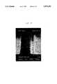
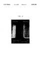
- FIGS. 6-8are photomicrographs of etched gate stacks formed in accordance with the process of the invention.
- Gate stackscan be made on a silicon oxide coated silicon substrate for example by depositing a first layer of a doped polysilicon onto a substrate, depositing, as by sputtering, a conductive refractory metal silicide layer, as of TiSi or WSi, and depositing a TEOS silicon oxide cap or hard mask over the silicide, see the above discussion with respect to FIGS. 1A and 1B.
- FIG. 5illustrates the profile of the above etched gate stack, wherein the numerals for the various layers are the same for like materials as for FIGS. 1A and 1B.
- FIG. 5illustrates that inadequate sidewall passivation has occurred, resulting in undercutting of both the silicide layer 15 and the polysilicon layer 14.
- the undercutting of the polysilicon layer 14is the most marked, and may be due to an increase in activity of plasma radicals near the end of the etch step.
- gate stackswere etched in the apparatus of FIGS. 2-4 using a precursor etch gas of HCl (20-100 sccm), chlorine (20-100 sccm), nitrogen (2-5 sccm) and oxygen (2-5 sccm). Nitrogen and oxygen are added for profile control and sidewall passivation. The addition of oxygen also improves the selectivity of the plasma precursor etch gas mixture to gate oxide.
- the transferred power to the planar coilwas 0-200 watts and the power to the substrate support was 50-200 watts.
- An etch ratio of 1:1 between the silicide and the polysilicon etch rateswas achieved.
- the etch uniformity across an 8 inch waferwas better than 5%.
- Etch selectivity to gate oxide of 50-100can be readily obtained for 50 nm lines and spaces using the above method.
- FIG. 6is a photomicrograph of an etched gate stack comprising TEOS silicon oxide over n-doped polysilicon. It is apparent that the etch is anisotropic with no undercutting.
- FIG. 7is a photomicrograph of another gate stack etched using the method of the invention, except that the gate stack includes a first layer of polysilicon, coated with a second sputtered tungsten silicide layer and a TEOS silicon oxide cap layer over the silicide layer. Again, the etch is very anisotropic, with only a very slight undercutting of the polysilicon layer.
- FIG. 8is a photomicrograph of still another gate stack etched in accordance with the method of the invention, except that this gate stack has a first layer of polysilicon, coated with a sputtered titanium silicide layer and a TEOS silicon oxide cap layer thereover. This etch also is highly anisotropic, with only a small amount of undercutting of the polysilicon layer.
Landscapes
- Engineering & Computer Science (AREA)
- Physics & Mathematics (AREA)
- Computer Hardware Design (AREA)
- Condensed Matter Physics & Semiconductors (AREA)
- General Physics & Mathematics (AREA)
- Manufacturing & Machinery (AREA)
- Microelectronics & Electronic Packaging (AREA)
- Power Engineering (AREA)
- Chemical & Material Sciences (AREA)
- Chemical Kinetics & Catalysis (AREA)
- General Chemical & Material Sciences (AREA)
- Plasma & Fusion (AREA)
- Drying Of Semiconductors (AREA)
- ing And Chemical Polishing (AREA)
Abstract
Description
Claims (7)
Priority Applications (7)
| Application Number | Priority Date | Filing Date | Title |
|---|---|---|---|
| US08/362,398US5591301A (en) | 1994-12-22 | 1994-12-22 | Plasma etching method |
| DE69534832TDE69534832T2 (en) | 1994-12-22 | 1995-11-03 | Improved plasma etching process |
| EP95117335AEP0718876B1 (en) | 1994-12-22 | 1995-11-03 | Improved plasma etching method |
| AT95117335TATE320082T1 (en) | 1994-12-22 | 1995-11-03 | IMPROVED PLASMA ETCHING PROCESS |
| TW084113288ATW410401B (en) | 1994-12-22 | 1995-12-13 | Improved plasma etching method |
| JP7349451AJPH08236513A (en) | 1994-12-22 | 1995-12-22 | Method of etching a substrate in plasma |
| KR1019950054324AKR100413894B1 (en) | 1994-12-22 | 1995-12-22 | Plasma Etching Method |
Applications Claiming Priority (1)
| Application Number | Priority Date | Filing Date | Title |
|---|---|---|---|
| US08/362,398US5591301A (en) | 1994-12-22 | 1994-12-22 | Plasma etching method |
Publications (1)
| Publication Number | Publication Date |
|---|---|
| US5591301Atrue US5591301A (en) | 1997-01-07 |
Family
ID=23425970
Family Applications (1)
| Application Number | Title | Priority Date | Filing Date |
|---|---|---|---|
| US08/362,398Expired - LifetimeUS5591301A (en) | 1994-12-22 | 1994-12-22 | Plasma etching method |
Country Status (7)
| Country | Link |
|---|---|
| US (1) | US5591301A (en) |
| EP (1) | EP0718876B1 (en) |
| JP (1) | JPH08236513A (en) |
| KR (1) | KR100413894B1 (en) |
| AT (1) | ATE320082T1 (en) |
| DE (1) | DE69534832T2 (en) |
| TW (1) | TW410401B (en) |
Cited By (20)
| Publication number | Priority date | Publication date | Assignee | Title |
|---|---|---|---|---|
| US5880033A (en)* | 1996-06-17 | 1999-03-09 | Applied Materials, Inc. | Method for etching metal silicide with high selectivity to polysilicon |
| US5900163A (en)* | 1996-05-08 | 1999-05-04 | Samsung Electronics Co., Ltd. | Methods for performing plasma etching operations on microelectronic structures |
| WO1999021495A1 (en)* | 1997-10-24 | 1999-05-06 | Fugo Richard J | Method of plasma incision of matter with a specifically tuned radiofrequency electromagnetic field generator |
| US5958266A (en)* | 1997-10-24 | 1999-09-28 | Fugo; Richard J. | Method of plasma incision of matter with a specifically tuned radiofrequency electromagnetic field generator |
| US6008139A (en)* | 1996-06-17 | 1999-12-28 | Applied Materials Inc. | Method of etching polycide structures |
| US6017825A (en)* | 1996-03-29 | 2000-01-25 | Lam Research Corporation | Etch rate loading improvement |
| US6207580B1 (en)* | 1997-12-30 | 2001-03-27 | International Business Machines Corporation | Method of plasma etching the tungsten silicide layer in the gate conductor stack formation |
| US6261967B1 (en) | 2000-02-09 | 2001-07-17 | Infineon Technologies North America Corp. | Easy to remove hard mask layer for semiconductor device fabrication |
| US6309926B1 (en) | 1998-12-04 | 2001-10-30 | Advanced Micro Devices | Thin resist with nitride hard mask for gate etch application |
| US6461974B1 (en) | 2000-10-06 | 2002-10-08 | Lam Research Corporation | High temperature tungsten etching process |
| US6479785B1 (en) | 1998-07-09 | 2002-11-12 | Richard J. Fugo | Device for plasma incision of mater with a specifically tuned radiofrequencty electromagnetic field generator |
| US20020177323A1 (en)* | 2000-05-16 | 2002-11-28 | Virinder Grewal | Gate etch process for 12 inch wafers |
| US6544896B1 (en) | 1999-03-05 | 2003-04-08 | Applied Materials Inc. | Method for enhancing etching of TiSix |
| US6562724B1 (en)* | 1997-06-09 | 2003-05-13 | Texas Instruments Incorporated | Self-aligned stack formation |
| US6642584B2 (en) | 2001-01-30 | 2003-11-04 | International Business Machines Corporation | Dual work function semiconductor structure with borderless contact and method of fabricating the same |
| US6787730B2 (en) | 1998-07-09 | 2004-09-07 | Damian Coccio | Device for plasma incision of matter with a specifically tuned radiofrequency electromagnetic field generator |
| US20080045941A1 (en)* | 2006-08-17 | 2008-02-21 | Fugo Richard J | Method and apparatus for plasma incision of cardiovascular tissue |
| US20090004862A1 (en)* | 2007-06-26 | 2009-01-01 | Hynix Semiconductor Inc. | Method for forming fine patterns in semiconductor device |
| US20120244693A1 (en)* | 2011-03-22 | 2012-09-27 | Tokyo Electron Limited | Method for patterning a full metal gate structure |
| US20140027813A1 (en)* | 2012-07-24 | 2014-01-30 | Marian Kuruc | Method of forming a semiconductor device having a patterned gate dielectric and structure therefor |
Families Citing this family (2)
| Publication number | Priority date | Publication date | Assignee | Title |
|---|---|---|---|---|
| JPH11145113A (en)* | 1997-11-13 | 1999-05-28 | Nec Corp | Etching method |
| KR101582542B1 (en)* | 2014-08-19 | 2016-01-05 | 국방과학연구소 | Device for Electromagnetic wave attenuation with large area plasma |
Citations (18)
| Publication number | Priority date | Publication date | Assignee | Title |
|---|---|---|---|---|
| US4030967A (en)* | 1976-08-16 | 1977-06-21 | Northern Telecom Limited | Gaseous plasma etching of aluminum and aluminum oxide |
| US4253907A (en)* | 1979-03-28 | 1981-03-03 | Western Electric Company, Inc. | Anisotropic plasma etching |
| US4297162A (en)* | 1979-10-17 | 1981-10-27 | Texas Instruments Incorporated | Plasma etching using improved electrode |
| US4444618A (en)* | 1983-03-03 | 1984-04-24 | General Electric Company | Processes and gas mixtures for the reactive ion etching of aluminum and aluminum alloys |
| US4798650A (en)* | 1987-03-27 | 1989-01-17 | Fujitsu Limited | Method of dry etching aluminum |
| US4838992A (en)* | 1987-05-27 | 1989-06-13 | Northern Telecom Limited | Method of etching aluminum alloys in semi-conductor wafers |
| US5112435A (en)* | 1985-10-11 | 1992-05-12 | Applied Materials, Inc. | Materials and methods for etching silicides, polycrystalline silicon and polycides |
| US5201990A (en)* | 1991-05-23 | 1993-04-13 | Applied Materials, Inc. | Process for treating aluminum surfaces in a vacuum apparatus |
| US5223085A (en)* | 1990-02-20 | 1993-06-29 | Mitsubishi Denki Kabushiki Kaisha | Plasma etching method with enhanced anisotropic property and apparatus thereof |
| US5248636A (en)* | 1987-07-16 | 1993-09-28 | Texas Instruments Incorporated | Processing method using both a remotely generated plasma and an in-situ plasma with UV irradiation |
| US5259922A (en)* | 1990-08-14 | 1993-11-09 | Matsushita Electric Industrial Co., Ltd. | Drying etching method |
| US5277750A (en)* | 1991-03-05 | 1994-01-11 | Siemens Aktiengesellschaft | Method for anisotropic dry etching of metallization layers, containing aluminum or aluminum alloys, in integrated semiconductor circuits |
| US5310456A (en)* | 1990-07-30 | 1994-05-10 | Sony Corporation | Dry etching method |
| US5320704A (en)* | 1990-11-28 | 1994-06-14 | Tokyo Electron Limited | Plasma etching apparatus |
| US5323053A (en)* | 1992-05-28 | 1994-06-21 | At&T Bell Laboratories | Semiconductor devices using epitaxial silicides on (111) surfaces etched in (100) silicon substrates |
| US5346578A (en)* | 1992-11-04 | 1994-09-13 | Novellus Systems, Inc. | Induction plasma source |
| US5401350A (en)* | 1993-03-08 | 1995-03-28 | Lsi Logic Corporation | Coil configurations for improved uniformity in inductively coupled plasma systems |
| US5449433A (en)* | 1994-02-14 | 1995-09-12 | Micron Semiconductor, Inc. | Use of a high density plasma source having an electrostatic shield for anisotropic polysilicon etching over topography |
Family Cites Families (6)
| Publication number | Priority date | Publication date | Assignee | Title |
|---|---|---|---|---|
| JPS62162362A (en)* | 1986-01-10 | 1987-07-18 | Mitsubishi Electric Corp | Mos integrated circuit and manufacture thereof |
| US4789426A (en)* | 1987-01-06 | 1988-12-06 | Harris Corp. | Process for performing variable selectivity polysilicon etch |
| JPS63215076A (en)* | 1987-03-04 | 1988-09-07 | Matsushita Electric Ind Co Ltd | Semiconductor integrated circuit device |
| US4948458A (en) | 1989-08-14 | 1990-08-14 | Lam Research Corporation | Method and apparatus for producing magnetically-coupled planar plasma |
| KR920014373A (en)* | 1990-12-03 | 1992-07-30 | 제임스 조렙 드롱 | Plasma Reactor Using VHF / UHF Resonant Antenna Source and Method of Generating Plasma |
| JPH0582481A (en)* | 1991-09-18 | 1993-04-02 | Nippon Telegr & Teleph Corp <Ntt> | Garnet film processing method |
- 1994
- 1994-12-22USUS08/362,398patent/US5591301A/ennot_activeExpired - Lifetime
- 1995
- 1995-11-03ATAT95117335Tpatent/ATE320082T1/ennot_activeIP Right Cessation
- 1995-11-03DEDE69534832Tpatent/DE69534832T2/ennot_activeExpired - Lifetime
- 1995-11-03EPEP95117335Apatent/EP0718876B1/ennot_activeExpired - Lifetime
- 1995-12-13TWTW084113288Apatent/TW410401B/ennot_activeIP Right Cessation
- 1995-12-22KRKR1019950054324Apatent/KR100413894B1/ennot_activeExpired - Fee Related
- 1995-12-22JPJP7349451Apatent/JPH08236513A/enactivePending
Patent Citations (18)
| Publication number | Priority date | Publication date | Assignee | Title |
|---|---|---|---|---|
| US4030967A (en)* | 1976-08-16 | 1977-06-21 | Northern Telecom Limited | Gaseous plasma etching of aluminum and aluminum oxide |
| US4253907A (en)* | 1979-03-28 | 1981-03-03 | Western Electric Company, Inc. | Anisotropic plasma etching |
| US4297162A (en)* | 1979-10-17 | 1981-10-27 | Texas Instruments Incorporated | Plasma etching using improved electrode |
| US4444618A (en)* | 1983-03-03 | 1984-04-24 | General Electric Company | Processes and gas mixtures for the reactive ion etching of aluminum and aluminum alloys |
| US5112435A (en)* | 1985-10-11 | 1992-05-12 | Applied Materials, Inc. | Materials and methods for etching silicides, polycrystalline silicon and polycides |
| US4798650A (en)* | 1987-03-27 | 1989-01-17 | Fujitsu Limited | Method of dry etching aluminum |
| US4838992A (en)* | 1987-05-27 | 1989-06-13 | Northern Telecom Limited | Method of etching aluminum alloys in semi-conductor wafers |
| US5248636A (en)* | 1987-07-16 | 1993-09-28 | Texas Instruments Incorporated | Processing method using both a remotely generated plasma and an in-situ plasma with UV irradiation |
| US5223085A (en)* | 1990-02-20 | 1993-06-29 | Mitsubishi Denki Kabushiki Kaisha | Plasma etching method with enhanced anisotropic property and apparatus thereof |
| US5310456A (en)* | 1990-07-30 | 1994-05-10 | Sony Corporation | Dry etching method |
| US5259922A (en)* | 1990-08-14 | 1993-11-09 | Matsushita Electric Industrial Co., Ltd. | Drying etching method |
| US5320704A (en)* | 1990-11-28 | 1994-06-14 | Tokyo Electron Limited | Plasma etching apparatus |
| US5277750A (en)* | 1991-03-05 | 1994-01-11 | Siemens Aktiengesellschaft | Method for anisotropic dry etching of metallization layers, containing aluminum or aluminum alloys, in integrated semiconductor circuits |
| US5201990A (en)* | 1991-05-23 | 1993-04-13 | Applied Materials, Inc. | Process for treating aluminum surfaces in a vacuum apparatus |
| US5323053A (en)* | 1992-05-28 | 1994-06-21 | At&T Bell Laboratories | Semiconductor devices using epitaxial silicides on (111) surfaces etched in (100) silicon substrates |
| US5346578A (en)* | 1992-11-04 | 1994-09-13 | Novellus Systems, Inc. | Induction plasma source |
| US5401350A (en)* | 1993-03-08 | 1995-03-28 | Lsi Logic Corporation | Coil configurations for improved uniformity in inductively coupled plasma systems |
| US5449433A (en)* | 1994-02-14 | 1995-09-12 | Micron Semiconductor, Inc. | Use of a high density plasma source having an electrostatic shield for anisotropic polysilicon etching over topography |
Cited By (33)
| Publication number | Priority date | Publication date | Assignee | Title |
|---|---|---|---|---|
| US6017825A (en)* | 1996-03-29 | 2000-01-25 | Lam Research Corporation | Etch rate loading improvement |
| US5900163A (en)* | 1996-05-08 | 1999-05-04 | Samsung Electronics Co., Ltd. | Methods for performing plasma etching operations on microelectronic structures |
| US5880033A (en)* | 1996-06-17 | 1999-03-09 | Applied Materials, Inc. | Method for etching metal silicide with high selectivity to polysilicon |
| US6008139A (en)* | 1996-06-17 | 1999-12-28 | Applied Materials Inc. | Method of etching polycide structures |
| US6562724B1 (en)* | 1997-06-09 | 2003-05-13 | Texas Instruments Incorporated | Self-aligned stack formation |
| AU736239B2 (en)* | 1997-10-24 | 2001-07-26 | Richard J. Fugo | Method of plasma incision of matter with a specifically tuned radiofrequency electromagnetic field generator |
| US5958266A (en)* | 1997-10-24 | 1999-09-28 | Fugo; Richard J. | Method of plasma incision of matter with a specifically tuned radiofrequency electromagnetic field generator |
| WO1999021495A1 (en)* | 1997-10-24 | 1999-05-06 | Fugo Richard J | Method of plasma incision of matter with a specifically tuned radiofrequency electromagnetic field generator |
| US6207580B1 (en)* | 1997-12-30 | 2001-03-27 | International Business Machines Corporation | Method of plasma etching the tungsten silicide layer in the gate conductor stack formation |
| US6867387B2 (en) | 1998-07-09 | 2005-03-15 | Richard J. Fugo | Device for plasma incision of matter with a specifically tuned radiofrequency electromagnetic field generator |
| US20050173383A1 (en)* | 1998-07-09 | 2005-08-11 | Damian Coccio | Device for plasma incision of matter with a specifically tuned radiofrequency electromagnetic field generator |
| US6787730B2 (en) | 1998-07-09 | 2004-09-07 | Damian Coccio | Device for plasma incision of matter with a specifically tuned radiofrequency electromagnetic field generator |
| US6479785B1 (en) | 1998-07-09 | 2002-11-12 | Richard J. Fugo | Device for plasma incision of mater with a specifically tuned radiofrequencty electromagnetic field generator |
| US7173211B2 (en) | 1998-07-09 | 2007-02-06 | Rjf Holdings Ii, Inc. | Device for plasma incision of matter with a specifically tuned radiofrequency electromagnetic field generator |
| US6309926B1 (en) | 1998-12-04 | 2001-10-30 | Advanced Micro Devices | Thin resist with nitride hard mask for gate etch application |
| US6544896B1 (en) | 1999-03-05 | 2003-04-08 | Applied Materials Inc. | Method for enhancing etching of TiSix |
| US6261967B1 (en) | 2000-02-09 | 2001-07-17 | Infineon Technologies North America Corp. | Easy to remove hard mask layer for semiconductor device fabrication |
| US20020177323A1 (en)* | 2000-05-16 | 2002-11-28 | Virinder Grewal | Gate etch process for 12 inch wafers |
| US6461974B1 (en) | 2000-10-06 | 2002-10-08 | Lam Research Corporation | High temperature tungsten etching process |
| US20040108555A1 (en)* | 2001-01-30 | 2004-06-10 | International Business Machines Corporation | Dual work function semiconductor structure with borderless contact and method of fabricating the same |
| US20050199966A1 (en)* | 2001-01-30 | 2005-09-15 | International Business Machines Corporation | Dual work function semiconductor structure with borderless contact and method of fabricating the same |
| US7015552B2 (en) | 2001-01-30 | 2006-03-21 | International Business Machines Corporation | Dual work function semiconductor structure with borderless contact and method of fabricating the same |
| US6642584B2 (en) | 2001-01-30 | 2003-11-04 | International Business Machines Corporation | Dual work function semiconductor structure with borderless contact and method of fabricating the same |
| US6908815B2 (en) | 2001-01-30 | 2005-06-21 | International Business Machines Corporation | Dual work function semiconductor structure with borderless contact and method of fabricating the same |
| US8088126B2 (en) | 2006-08-17 | 2012-01-03 | Fugo Richard J | Method and apparatus for plasma incision of cardiovascular tissue |
| US20080045941A1 (en)* | 2006-08-17 | 2008-02-21 | Fugo Richard J | Method and apparatus for plasma incision of cardiovascular tissue |
| US8137341B2 (en) | 2006-08-17 | 2012-03-20 | Richard J Fugo | Methods and apparatus for plasma incision of tissue |
| US7919414B2 (en)* | 2007-06-26 | 2011-04-05 | Hynix Semiconductor Inc. | Method for forming fine patterns in semiconductor device |
| US20090004862A1 (en)* | 2007-06-26 | 2009-01-01 | Hynix Semiconductor Inc. | Method for forming fine patterns in semiconductor device |
| US20120244693A1 (en)* | 2011-03-22 | 2012-09-27 | Tokyo Electron Limited | Method for patterning a full metal gate structure |
| US20140027813A1 (en)* | 2012-07-24 | 2014-01-30 | Marian Kuruc | Method of forming a semiconductor device having a patterned gate dielectric and structure therefor |
| US8946002B2 (en)* | 2012-07-24 | 2015-02-03 | Semiconductor Components Industries, Llc | Method of forming a semiconductor device having a patterned gate dielectric and structure therefor |
| US9385202B2 (en) | 2012-07-24 | 2016-07-05 | Semiconductor Components Industries, Llc | Semiconductor device having a patterned gate dielectric |
Also Published As
| Publication number | Publication date |
|---|---|
| KR960026340A (en) | 1996-07-22 |
| ATE320082T1 (en) | 2006-03-15 |
| EP0718876B1 (en) | 2006-03-08 |
| TW410401B (en) | 2000-11-01 |
| JPH08236513A (en) | 1996-09-13 |
| DE69534832T2 (en) | 2006-09-28 |
| KR100413894B1 (en) | 2004-04-21 |
| DE69534832D1 (en) | 2006-05-04 |
| EP0718876A3 (en) | 1998-05-20 |
| EP0718876A2 (en) | 1996-06-26 |
Similar Documents
| Publication | Publication Date | Title |
|---|---|---|
| US5591301A (en) | Plasma etching method | |
| US7049244B2 (en) | Method for enhancing silicon dioxide to silicon nitride selectivity | |
| US5449433A (en) | Use of a high density plasma source having an electrostatic shield for anisotropic polysilicon etching over topography | |
| US5429710A (en) | Dry etching method | |
| US6583065B1 (en) | Sidewall polymer forming gas additives for etching processes | |
| US5997757A (en) | Method of forming connection hole | |
| US5880033A (en) | Method for etching metal silicide with high selectivity to polysilicon | |
| US6815825B2 (en) | Semiconductor devices having gradual slope contacts | |
| EP0814500B1 (en) | Method for etching polycide structures | |
| EP0954877B1 (en) | Method for reducing plasma-induced charging damage | |
| WO1997036322A1 (en) | Methods and apparatus for minimizing etch rate loading | |
| KR20020070255A (en) | Multiple stage cleaning for plasma etching chambers | |
| JPS61179872A (en) | Apparatus and method for magnetron-enhanced plasma-assisted chemical vapor deposition | |
| US20030000913A1 (en) | Highly selective process for etching oxide over nitride using hexafluorobutadiene | |
| US6432832B1 (en) | Method of improving the profile angle between narrow and wide features | |
| US6562722B2 (en) | Method and apparatus for dry etching | |
| US6410451B2 (en) | Techniques for improving etching in a plasma processing chamber | |
| US20010005634A1 (en) | Dry etching method and manufacturing method of semiconductor device for realizing high selective etching | |
| KR100747671B1 (en) | Dry etching method and manufacturing method of semiconductor device | |
| US5880037A (en) | Oxide etch process using a mixture of a fluorine-substituted hydrocarbon and acetylene that provides high selectivity to nitride and is suitable for use on surfaces of uneven topography | |
| US6008132A (en) | Dry etching suppressing formation of notch | |
| US6506687B1 (en) | Dry etching device and method of producing semiconductor devices | |
| JPH09172005A (en) | Method for plasma etching oxides that can show high selectivity for nitrides | |
| JPH0774147A (en) | Method and apparatus for dry etching | |
| US6686294B2 (en) | Method and apparatus for etching silicon nitride film and manufacturing method of semiconductor device |
Legal Events
| Date | Code | Title | Description |
|---|---|---|---|
| AS | Assignment | Owner name:SIEMENS COMPONENTS, INC., CALIFORNIA Free format text:ASSIGNMENT OF ASSIGNORS INTEREST;ASSIGNOR:GREWAL, VIRINDER S.;REEL/FRAME:007426/0290 Effective date:19950227 | |
| AS | Assignment | Owner name:SIEMENS AKTIENGESELLSCHAFT, GERMANY Free format text:ASSIGNMENT OF ASSIGNORS INTEREST;ASSIGNOR:SIEMENS COMPONENTS, INC.;REEL/FRAME:007508/0676 Effective date:19950531 | |
| STCF | Information on status: patent grant | Free format text:PATENTED CASE | |
| FEPP | Fee payment procedure | Free format text:PAYOR NUMBER ASSIGNED (ORIGINAL EVENT CODE: ASPN); ENTITY STATUS OF PATENT OWNER: LARGE ENTITY | |
| FPAY | Fee payment | Year of fee payment:4 | |
| FPAY | Fee payment | Year of fee payment:8 | |
| AS | Assignment | Owner name:INFINEON TECHNOLOGIES AG, GERMANY Free format text:ASSIGNMENT OF ASSIGNORS INTEREST;ASSIGNOR:SIEMENS AKTIENGESELLSCHAFT;REEL/FRAME:015386/0643 Effective date:20041026 | |
| FPAY | Fee payment | Year of fee payment:12 | |
| AS | Assignment | Owner name:QIMONDA AG, GERMANY Free format text:ASSIGNMENT OF ASSIGNORS INTEREST;ASSIGNOR:INFINEON TECHNOLOGIES AG;REEL/FRAME:023828/0001 Effective date:20060425 |