US5587945A - CMOS EEPROM cell with tunneling window in the read path - Google Patents
CMOS EEPROM cell with tunneling window in the read pathDownload PDFInfo
- Publication number
- US5587945A US5587945AUS08/554,092US55409295AUS5587945AUS 5587945 AUS5587945 AUS 5587945AUS 55409295 AUS55409295 AUS 55409295AUS 5587945 AUS5587945 AUS 5587945A
- Authority
- US
- United States
- Prior art keywords
- source
- floating gate
- common floating
- transistor
- nmos transistor
- Prior art date
- Legal status (The legal status is an assumption and is not a legal conclusion. Google has not performed a legal analysis and makes no representation as to the accuracy of the status listed.)
- Expired - Lifetime
Links
- 230000005641tunnelingEffects0.000titleclaimsabstractdescription26
- 239000003990capacitorSubstances0.000claimsabstractdescription38
- 238000000034methodMethods0.000claims2
- 239000007943implantSubstances0.000description25
- 239000000758substrateSubstances0.000description12
- 229910021420polycrystalline siliconInorganic materials0.000description5
- 229920005591polysiliconPolymers0.000description5
- 238000004549pulsed laser depositionMethods0.000description3
- 230000000295complement effectEffects0.000description2
- 101100328883Arabidopsis thaliana COL1 geneProteins0.000description1
- 101100328886Caenorhabditis elegans col-2 geneProteins0.000description1
- 230000008878couplingEffects0.000description1
- 238000010168coupling processMethods0.000description1
- 238000005859coupling reactionMethods0.000description1
- 238000005516engineering processMethods0.000description1
- 238000012986modificationMethods0.000description1
- 230000004048modificationEffects0.000description1
- 230000001105regulatory effectEffects0.000description1
Images


Classifications
- G—PHYSICS
- G11—INFORMATION STORAGE
- G11C—STATIC STORES
- G11C16/00—Erasable programmable read-only memories
- G11C16/02—Erasable programmable read-only memories electrically programmable
- G11C16/04—Erasable programmable read-only memories electrically programmable using variable threshold transistors, e.g. FAMOS
- G11C16/0408—Erasable programmable read-only memories electrically programmable using variable threshold transistors, e.g. FAMOS comprising cells containing floating gate transistors
- G11C16/0441—Erasable programmable read-only memories electrically programmable using variable threshold transistors, e.g. FAMOS comprising cells containing floating gate transistors comprising cells containing multiple floating gate devices, e.g. separate read-and-write FAMOS transistors with connected floating gates
- G11C16/045—Floating gate memory cells with both P and N channel memory transistors, usually sharing a common floating gate
- G—PHYSICS
- G11—INFORMATION STORAGE
- G11C—STATIC STORES
- G11C16/00—Erasable programmable read-only memories
- G11C16/02—Erasable programmable read-only memories electrically programmable
- G11C16/04—Erasable programmable read-only memories electrically programmable using variable threshold transistors, e.g. FAMOS
- G11C16/0408—Erasable programmable read-only memories electrically programmable using variable threshold transistors, e.g. FAMOS comprising cells containing floating gate transistors
- G11C16/0441—Erasable programmable read-only memories electrically programmable using variable threshold transistors, e.g. FAMOS comprising cells containing floating gate transistors comprising cells containing multiple floating gate devices, e.g. separate read-and-write FAMOS transistors with connected floating gates
- H—ELECTRICITY
- H10—SEMICONDUCTOR DEVICES; ELECTRIC SOLID-STATE DEVICES NOT OTHERWISE PROVIDED FOR
- H10B—ELECTRONIC MEMORY DEVICES
- H10B69/00—Erasable-and-programmable ROM [EPROM] devices not provided for in groups H10B41/00 - H10B63/00, e.g. ultraviolet erasable-and-programmable ROM [UVEPROM] devices
- G—PHYSICS
- G11—INFORMATION STORAGE
- G11C—STATIC STORES
- G11C2216/00—Indexing scheme relating to G11C16/00 and subgroups, for features not directly covered by these groups
- G11C2216/02—Structural aspects of erasable programmable read-only memories
- G11C2216/10—Floating gate memory cells with a single polysilicon layer
Definitions
- the present inventionrelates to circuitry for a programmable CMOS memory cell, the CMOS memory cell having PMOS and NMOS transistors with a common floating gate. More particularly, the present invention relates to such programmable CMOS memory cells which can be utilized in a programmable logic device (PLD).
- PLDprogrammable logic device
- FIG. 1illustrates a first type conventional CMOS memory cell having a PMOS transistor 102 and an NMOS transistor 104 with a common floating gate.
- the first type CMOS cellincludes two capacitors 106 and 108 which are utilized to program and erase the common floating gate.
- Capacitor 106supplies voltage from an array control gate (ACG) node.
- An NMOS pass transistor 110supplies a word control (WC) voltage to capacitor 108 as controlled by a word line (WL) voltage supplied to its gate.
- ACGarray control gate
- NMOS pass transistor 110supplies a word control (WC) voltage to capacitor 108 as controlled by a word line (WL) voltage supplied to its gate.
- drains of transistors 102 and 104are connected together to form an output.
- Bias voltageis provided to the source of PMOS transistor 102 from a chip Vcc pin.
- Bias voltageis provided to the source of the NMOS transistor 104 through a chip ground or Vss pin.
- the CMOS memory cell of FIG. 1is disclosed in U.S. Pat. No. 5,272,368 entitled “Complementary Low Power Non-Volatile Reconfigurable EECELL,” and in U.S. Pat. No. 4,885,719 entitled “Improved Logic Cell Array Using CMOS E 2 PROM Cells.”
- FIG. 2shows a layout for the first type CMOS cell of FIG. 1 as formed in a p type substrate.
- capacitor 106includes an n+ type program junction implant region 202 formed in the p substrate. Separating the n+ type implant region 202 from the common floating gate (F.G.) 204 is an oxide layer approximately 150 ⁇ thick.
- Capacitor 108includes an n+program junction implant region 206 formed in the p type substrate. Overlying the n+ type implant region 206 is the floating gate 204 which is separated from the implant region 206 by a gate oxide which includes a 150 ⁇ portion and a 85 ⁇ tunneling portion 208. The 85 ⁇ tunneling portion 208 enables charge to be applied to the floating gate 204 during program and removed during erase.
- transistor 110is formed by a polysilicon (POLY) word line (WL) region on the substrate with a portion of the WL region adjacent the n+ implant region 206 and another portion adjacent an additional n+ implant region 210.
- Transistor 104includes two n+ implant regions 212 and 214 in the p substrate. A gate oxide region of approximately 150 ⁇ separates a channel between regions 212 and 214 from the common floating gate 204.
- Transistor 102includes two p type regions 216 and 218 in a n+ type well 220 which is included in the p type substrate. A gate oxide region of approximately 150 ⁇ separates the channel between regions 216 and 218 from the common floating gate 204.
- CMOS memory cell of FIG. 1Typical voltages applied for program, erase and read of the CMOS memory cell of FIG. 1 are listed in Table I below.
- programmingindicates electrons are removed from the common floating gate, while erase indicates that electrons are added to the common floating gate.
- Vppindicates a programming voltage, typically of 12 volts.
- Vpp+indicates the Vpp voltage plus an n channel threshold, typically totaling 13.8 volts.
- Vccindicates a chip power supply pin voltage, typically of 5 volts.
- FIG. 3shows a second type CMOS memory cell design including a PMOS transistor 302 and an NMOS transistor 304 with a common floating gate. Unlike the capacitors 102 and 104 utilized in the first type CMOS memory cell of FIG. 1, the second type CMOS cell utilizes capacitor 306 and tunneling oxide regions in transistors 302 and 304 for program and erase.
- the capacitor 306is connected between an array control gate (ACG) node and the common floating gate.
- ACGarray control gate
- CMOS cell of FIG. 3the drains of transistors 302 and 304 are connected together to form the CMOS cell output.
- An additional PMOS pass gate transistor 310has a drain connected to the source of PMOS transistor 302, a source connected to receive a word control (WC) voltage and a gate connected to receive a word line (WL) voltage.
- FIG. 4shows the layout for the cell of FIG. 3.
- the capacitor 306includes an n+ type program junction implant region 402 formed in the p type substrate. Separated from the n+ type implant region 402 by a 150 ⁇ thick gate oxide region is the common floating gate (F.G.) 406.
- the tunneling oxide windows 430 and 432 of approximately 85 ⁇are provided between the floating gate 406 and the channel regions of respective transistors 302 and 304.
- the remaining regions of the common floating gate 406are separated from the substrate by a 185 ⁇ oxide layer.
- the channel region of the NMOS transistor 304is formed between its n+ source and drain implant regions 410 and 412.
- the channel region of the PMOS transistor 302is formed in an n+ well between p+ implant regions 414 and 416.
- the PMOS pass transistor 310is formed in the same n+ well as transistor 302, using the n+ implant region 416 as its source, an additional implant region 418 as its drain, and a polysilicon wordline (WL) forming its gate.
- CMOS memory cellprogrammed through the tunneling window of PMOS transistor 302
- current leakagecan occur to cause a disturb condition.
- Such a disturb conditionoccurs where electrons are injected onto the common floating gate in a CMOS cell which is not to be programmed.
- the current leakage during programmingcan occur because of charge storage in a large n well in which the PMOS transistors 302 and 310, as well as PMOS transistors of other CMOS cells are formed.
- a single n wellis typically shared by a column of cells which all receive the same voltage WC during programming of a particular cell in the column.
- a WL voltage of Vccis applied, but in cells not to be programmed, a WL voltage of Vpp+is applied.
- the Vpp+WL voltageis applied to assure that the source of the PMOS transistors of unselected cells are floating, floating indicating a high impedance (Hiz) state.
- Hizhigh impedance
- a large number of cells in an arraywill require a long Vss line, the long Vss line then having a significant capacitive component, enabling charge storage.
- an additional NMOS transistor 500can be added to the CMOS memory cell of FIG. 3, as shown in FIG. 5.
- Transistor 500enables disconnection of the source of NMOS transistor 304 from the Vss line during programming to prevent a disturb condition.
- Such a CMOS memory cellis described in more detail in U.S. patent application Ser. No. 08/447,991, entitled “A Completely Complementary MOS Memory Cell With Tunneling Through The NMOS and PMOS Transistor During Program And Erase, filed May 23, 1995.
- the additional transistor 500does help prevent a disturb condition, maintaining the drain of PMOS transistor 302 floating remains difficult, making a disturb condition likely.
- FIG. 6shows a programmable memory cell most commonly used in PLDs.
- the memory cell of FIG. 6is manufactured similar to the first type cell of FIG. 1, with two capacitors 606 and 608 to control programming of a floating gate.
- the floating gateis coupled only to a single transistor 604.
- transistor 610is utilized to apply voltages to capacitor 608.
- the gate voltage of transistor 610is also applied to an additional NMOS transistor 602.
- FIG. 7shows the connections of two array cells 701 and 702 in a PLD.
- each array cell 701 and 702receives an input signal COL1 and COL2 as an enable signal EN.
- Each of cells 701 and 702further has one connection to a product term (PT) line and an additional connection to a product term ground (PTG) line.
- the PT lineforms an input to a buffer 712 included in a sense amplifier 710.
- the PTG lineprovides a connection to Vss in the sense amplifier 710.
- the sense amplifier 710also includes a current source 714 connected to the input of the buffer 312.
- Array cells 701 and 702are programmed to provide a connection from the PT to the PTG line, the connection being provided when the array cell receives an appropriate EN signal.
- CMOS memory cell of FIG. 5is advantageous because it enables zero power operation, zero power operation indicating that the component does not continually draw power when the component is not changing states.
- the present inventionprovides a CMOS memory cell which can be utilized in a PLD.
- the present inventionfurther provides a CMOS memory cell more compatible to current technology used in PLDs than the second type cells which include tunneling windows in the NMOS and PMOS transistors of the CMOS cell.
- the present inventionfurther does not have the potential disturb condition of the second type cells.
- the present inventionis a CMOS memory cell including PMOS and NMOS transistors with a common floating gate.
- the CMOS memory cell of the present inventionincludes a first capacitor connecting the floating gate to an ACG node as with cell 106 of FIG. 1.
- the CMOS cell of the present inventionfurther includes a second tunneling capacitor having a first end connected to the floating gate, similar to the first type CMOS cell of FIG. 1.
- the second end of the tunneling capacitoris also connected to the source of the NMOS transistor which shares the common floating gate.
- the CMOS cell of the present inventionincludes an NMOS pass transistor to supply a word control (WC) voltage to the second end of the tunneling capacitor as controlled by a word line (WL) voltage applied to its gate.
- WCword control
- WLword line
- FIG. 1illustrates a first configuration of a first type conventional CMOS memory cell
- FIG. 2shows the layout for the CMOS memory cell of FIG. 1;
- FIG. 3shows circuitry for a second type CMOS memory cell
- FIG. 4shows the layout for the CMOS cell of FIG. 3
- FIG. 5shows the CMOS cell of FIG. 4 with an additional transistor added to prevent a disturb condition
- FIG. 6shows a conventional programmable memory cell most commonly used in PLDs
- FIG. 7shows the connections of two array cells in a PLD
- FIG. 8illustrates a CMOS memory cell of the present invention
- FIG. 9shows the layout for the circuit of FIG. 8.
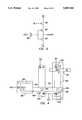
- FIG. 8illustrates a CMOS memory cell of the present invention.
- the CMOS memory cellincludes a PMOS transistor 802 and an NMOS transistor 804 having a common floating gate. Similar to the first type memory cell shown in FIG. 1, the CMOS memory cell of FIG. 8 includes a tunneling capacitor 808 having a tunneling window used to add or subtract charge to the common floating gate during program or erase.
- the tunneling capacitorhas a first end connected to the common floating gate and a second end connected to the drain of a pass gate 810.
- the pass gate 810has a source connected to a word control (WC) voltage node, and a gate connected to a word line (WL) voltage node.
- FIG. 8includes a capacitor 806 coupling an array control gate (ACG) node to the common floating gate.
- ACGarray control gate
- the second end of capacitor 808 which is connected to the drain of NMOS pass transistor 810is also connected to the source of NMOS transistor 804.
- the CMOS cell of FIG. 8can be utilized as a cell in a PLD configured as shown in FIG. 7.
- FIG. 9shows the layout for the circuit of FIG. 8.
- capacitor 806includes an n+ type program junction implant region 902 formed in the p substrate. Separating the n+ type implant region 902 from the common floating gate (F.G.) 904 is an oxide layer approximately 150 ⁇ thick. A contact connected to the n+ implant region 902 provides a connection to the ACG node.
- F.G.common floating gate
- Capacitor 808includes an n+ program junction implant region 906 formed in the p type substrate. Overlying the n+ type implant region 906 is the floating gate 904 which is separated from the implant region 906 by a gate oxide which includes a 150 ⁇ portion and a 85 ⁇ tunneling portion 908. The 85 ⁇ tunneling region 908 enables charge to be applied to the floating gate 904 during program and removed during erase.
- transistor 810is formed by a polysilicon (POLY) word line (WL) region on the substrate with a portion of the WL region adjacent the n+ implant region 906 and another portion adjacent an additional n+ implant region 910.
- POLYpolysilicon
- a contact region provided in the n+ implant region 910provides a connection to the WC node.
- Transistor 804shares the n+ implant region 906 of capacitor 808 and includes an additional n+ implant region 912.
- a gate oxide region of approximately 150 ⁇separates a channel between regions 906 and 912 from the common floating gate 904.
- a contact connected to region 912provides a connection to an output node.
- transistor 802includes two p type regions 916 and 918 in a n+ type well 920 which is included in the p type substrate.
- a gate oxide region of approximately 150 ⁇separates the channel between regions 916 and 918 from the common floating gate 904.
- a contact connected to region 916provides a connection to an output node.
- a contact to region 918provides a connection to Vcc.
- Voltages applied to the circuitry of FIG. 8are altered from voltages applied with the circuitry of FIG. 1 to account for the connection of one end of capacitor 808 and the source of the NMOS transistor 804 to the drain of NMOS pass transistor 810.
- Vccwas set to zero and the source of the NMOS transistor, or Vss was set to zero.
- Vpptypically being 12 V, must be applied to one end of capacitor 808 to enable programming.
- Vppis thus, likewise applied to the source of transistor 804 during programming. Since programming occurs through a tunneling region of capacitor 808, instead of through a common floating gate of PMOS and NMOS transistors as in the second type cell of FIG. 3, voltages on the PMOS and NMOS cells are not as critical during programming.
- the source of the NMOS transistor 804 at Vppthe source of PMOS transistor 802 can be floating, or at a high impedance (Hiz) level and programming still occur.
- the Hiz levelis used instead of at a zero volt level for Vcc as in FIG. 1 because with Vcc at zero volts, a path would be created to ground from the source of the NMOS transistor 804 which would drain the power supply providing the programming voltage Vpp.
- Vccwas set to Vpp and the source of the NMOS transistor, or Vss was set to Vpp. Such voltages were previously applied to prevent current leakage through the PMOS and NMOS transistors of a CMOS cell.
- the end of capacitor 808 connected to the source of NMOS transistor 804must be set to zero volts.
- Vccis set to a Hiz level for the circuit of FIG. 8 to prevent such a path to ground.
- the source of the NMOS transistor 804must be maintained at zero volts.
- the voltage applied to capacitor 808 at the source of NMOS transistor 804is likewise zero volts.
- the voltage on the floating gateshould be maintained at a voltage of approximately Vcc/2.
- the ACG voltageis set at Vcc/2, or slightly higher.
- CMOS memory cellshave previously not been considered practical because the threshold of the PMOS transistor, such as 802, is typically referenced to Vcc.
- Vccbeing a voltage supplied from an external source to the Vcc pin, unregulated variations in Vcc occur. Such variations in Vcc require that an unacceptably high voltage be applied to the common floating gate to assure PMOS transistor 802 can be turned off.
- a regulated voltagefrom a voltage reference to the source of PMOS transistor 802, rather than directly from Vcc, use of a CMOS memory cell becomes practical.
Landscapes
- Engineering & Computer Science (AREA)
- Microelectronics & Electronic Packaging (AREA)
- Non-Volatile Memory (AREA)
- Read Only Memory (AREA)
Abstract
Description
TABLE I ______________________________________ WC WL ACG Vcc Vss ______________________________________ Program Vpp Vpp+ 0 0 0 Erase 0 Vcc Vpp+ Vpp Vpp Read Vcc/2 Vcc Vcc/2 Vcc 0 ______________________________________
TABLE II ______________________________________ WC WL ACG Vss ______________________________________ Program Vpp Vcc 0 Hiz Erase Hiz 0 Vpp 0 Read Vcc 0 Vcc/2 0 ______________________________________
TABLE III ______________________________________ WC WL ACG Vcc ______________________________________ Program Vpp Vpp+ 0 Hiz Erase 0 Vcc Vpp+ Hiz Read 0 Vcc Vcc/2 Vcc ______________________________________
Claims (6)
Priority Applications (1)
| Application Number | Priority Date | Filing Date | Title |
|---|---|---|---|
| US08/554,092US5587945A (en) | 1995-11-06 | 1995-11-06 | CMOS EEPROM cell with tunneling window in the read path |
Applications Claiming Priority (1)
| Application Number | Priority Date | Filing Date | Title |
|---|---|---|---|
| US08/554,092US5587945A (en) | 1995-11-06 | 1995-11-06 | CMOS EEPROM cell with tunneling window in the read path |
Publications (1)
| Publication Number | Publication Date |
|---|---|
| US5587945Atrue US5587945A (en) | 1996-12-24 |
Family
ID=24212040
Family Applications (1)
| Application Number | Title | Priority Date | Filing Date |
|---|---|---|---|
| US08/554,092Expired - LifetimeUS5587945A (en) | 1995-11-06 | 1995-11-06 | CMOS EEPROM cell with tunneling window in the read path |
Country Status (1)
| Country | Link |
|---|---|
| US (1) | US5587945A (en) |
Cited By (71)
| Publication number | Priority date | Publication date | Assignee | Title |
|---|---|---|---|---|
| WO1998029907A3 (en)* | 1997-01-02 | 1998-09-11 | John M Caywood | Low voltage single supply cmos electrically erasable read-only memory |
| US5844912A (en)* | 1997-04-01 | 1998-12-01 | Advanced Micro Devices, Inc. | Fast verify for CMOS memory cells |
| US5892709A (en)* | 1997-05-09 | 1999-04-06 | Motorola, Inc. | Single level gate nonvolatile memory device and method for accessing the same |
| US5903494A (en)* | 1994-03-30 | 1999-05-11 | Sgs-Thomson Microelectronics S.A. | Electrically programmable memory cell |
| US5942780A (en)* | 1996-08-09 | 1999-08-24 | Advanced Micro Devices, Inc. | Integrated circuit having, and process providing, different oxide layer thicknesses on a substrate |
| US6201732B1 (en) | 1997-01-02 | 2001-03-13 | John M. Caywood | Low voltage single CMOS electrically erasable read-only memory |
| US6214666B1 (en) | 1998-12-18 | 2001-04-10 | Vantis Corporation | Method of forming a non-volatile memory device |
| US6215700B1 (en)* | 1999-01-07 | 2001-04-10 | Vantis Corporation | PMOS avalanche programmed floating gate memory cell structure |
| US6232631B1 (en) | 1998-12-21 | 2001-05-15 | Vantis Corporation | Floating gate memory cell structure with programming mechanism outside the read path |
| US6282123B1 (en) | 1998-12-21 | 2001-08-28 | Lattice Semiconductor Corporation | Method of fabricating, programming, and erasing a dual pocket two sided program/erase non-volatile memory cell |
| US6294809B1 (en) | 1998-12-28 | 2001-09-25 | Vantis Corporation | Avalanche programmed floating gate memory cell structure with program element in polysilicon |
| US6294810B1 (en) | 1998-12-22 | 2001-09-25 | Vantis Corporation | EEPROM cell with tunneling at separate edge and channel regions |
| US6294811B1 (en) | 1999-02-05 | 2001-09-25 | Vantis Corporation | Two transistor EEPROM cell |
| US6326663B1 (en) | 1999-03-26 | 2001-12-04 | Vantis Corporation | Avalanche injection EEPROM memory cell with P-type control gate |
| US6388464B1 (en) | 1999-12-30 | 2002-05-14 | Cypress Semiconductor Corp. | Configurable memory for programmable logic circuits |
| US6404006B2 (en)* | 1998-12-01 | 2002-06-11 | Vantis Corporation | EEPROM cell with tunneling across entire separated channels |
| US6424000B1 (en) | 1999-05-11 | 2002-07-23 | Vantis Corporation | Floating gate memory apparatus and method for selected programming thereof |
| US6608500B1 (en) | 2000-03-31 | 2003-08-19 | Cypress Semiconductor Corp. | I/O architecture/cell design for programmable logic device |
| US6660579B1 (en) | 2002-04-24 | 2003-12-09 | Lattice Semiconductor Corp. | Zero power memory cell with improved data retention |
| US6788574B1 (en)* | 2001-12-06 | 2004-09-07 | Virage Logic Corporation | Electrically-alterable non-volatile memory cell |
| US6822254B1 (en)* | 2003-04-04 | 2004-11-23 | Michael L. Lovejoy | Non-volatile memory cell |
| US6842375B1 (en) | 2001-12-06 | 2005-01-11 | Virage Logic Corporation | Methods and apparatuses for maintaining information stored in a non-volatile memory cell |
| US6864710B1 (en) | 1999-12-30 | 2005-03-08 | Cypress Semiconductor Corp. | Programmable logic device |
| US6992938B1 (en) | 2001-12-06 | 2006-01-31 | Virage Logic Corporation | Methods and apparatuses for test circuitry for a dual-polarity non-volatile memory cell |
| US7130213B1 (en) | 2001-12-06 | 2006-10-31 | Virage Logic Corporation | Methods and apparatuses for a dual-polarity non-volatile memory cell |
| US7187212B1 (en)* | 2004-10-26 | 2007-03-06 | National Semiconductor Corporation | System and method for providing a fast turn on bias circuit for current mode logic transmitters |
| US20070145459A1 (en)* | 2005-12-22 | 2007-06-28 | Geun-Sook Park | EEPROM devices and methods of operating and fabricating the same |
| US7737724B2 (en) | 2007-04-17 | 2010-06-15 | Cypress Semiconductor Corporation | Universal digital block interconnection and channel routing |
| US7761845B1 (en) | 2002-09-09 | 2010-07-20 | Cypress Semiconductor Corporation | Method for parameterizing a user module |
| US7765095B1 (en) | 2000-10-26 | 2010-07-27 | Cypress Semiconductor Corporation | Conditional branching in an in-circuit emulation system |
| US7770113B1 (en) | 2001-11-19 | 2010-08-03 | Cypress Semiconductor Corporation | System and method for dynamically generating a configuration datasheet |
| US7774190B1 (en) | 2001-11-19 | 2010-08-10 | Cypress Semiconductor Corporation | Sleep and stall in an in-circuit emulation system |
| US7796464B1 (en) | 2003-06-27 | 2010-09-14 | Cypress Semiconductor Corporation | Synchronous memory with a shadow-cycle counter |
| US7825688B1 (en) | 2000-10-26 | 2010-11-02 | Cypress Semiconductor Corporation | Programmable microcontroller architecture(mixed analog/digital) |
| US7844437B1 (en) | 2001-11-19 | 2010-11-30 | Cypress Semiconductor Corporation | System and method for performing next placements and pruning of disallowed placements for programming an integrated circuit |
| US7893724B2 (en) | 2004-03-25 | 2011-02-22 | Cypress Semiconductor Corporation | Method and circuit for rapid alignment of signals |
| US7893772B1 (en) | 2007-12-03 | 2011-02-22 | Cypress Semiconductor Corporation | System and method of loading a programmable counter |
| US8026739B2 (en) | 2007-04-17 | 2011-09-27 | Cypress Semiconductor Corporation | System level interconnect with programmable switching |
| US20110235425A1 (en)* | 2010-03-25 | 2011-09-29 | Pavel Poplevine | Method of directly reading output voltage to determine data stored in a non-volatile memory cell |
| US8040266B2 (en) | 2007-04-17 | 2011-10-18 | Cypress Semiconductor Corporation | Programmable sigma-delta analog-to-digital converter |
| US8049569B1 (en) | 2007-09-05 | 2011-11-01 | Cypress Semiconductor Corporation | Circuit and method for improving the accuracy of a crystal-less oscillator having dual-frequency modes |
| US8069428B1 (en) | 2001-10-24 | 2011-11-29 | Cypress Semiconductor Corporation | Techniques for generating microcontroller configuration information |
| US8069405B1 (en) | 2001-11-19 | 2011-11-29 | Cypress Semiconductor Corporation | User interface for efficiently browsing an electronic document using data-driven tabs |
| US8067948B2 (en) | 2006-03-27 | 2011-11-29 | Cypress Semiconductor Corporation | Input/output multiplexer bus |
| US8069436B2 (en) | 2004-08-13 | 2011-11-29 | Cypress Semiconductor Corporation | Providing hardware independence to automate code generation of processing device firmware |
| US8078894B1 (en) | 2007-04-25 | 2011-12-13 | Cypress Semiconductor Corporation | Power management architecture, method and configuration system |
| US8078970B1 (en) | 2001-11-09 | 2011-12-13 | Cypress Semiconductor Corporation | Graphical user interface with user-selectable list-box |
| US8085067B1 (en) | 2005-12-21 | 2011-12-27 | Cypress Semiconductor Corporation | Differential-to-single ended signal converter circuit and method |
| US8085100B2 (en) | 2005-02-04 | 2011-12-27 | Cypress Semiconductor Corporation | Poly-phase frequency synthesis oscillator |
| US8092083B2 (en) | 2007-04-17 | 2012-01-10 | Cypress Semiconductor Corporation | Temperature sensor with digital bandgap |
| US8103497B1 (en) | 2002-03-28 | 2012-01-24 | Cypress Semiconductor Corporation | External interface for event architecture |
| US8103496B1 (en) | 2000-10-26 | 2012-01-24 | Cypress Semicondutor Corporation | Breakpoint control in an in-circuit emulation system |
| US8120408B1 (en) | 2005-05-05 | 2012-02-21 | Cypress Semiconductor Corporation | Voltage controlled oscillator delay cell and method |
| US8130025B2 (en) | 2007-04-17 | 2012-03-06 | Cypress Semiconductor Corporation | Numerical band gap |
| US8149048B1 (en) | 2000-10-26 | 2012-04-03 | Cypress Semiconductor Corporation | Apparatus and method for programmable power management in a programmable analog circuit block |
| US8160864B1 (en) | 2000-10-26 | 2012-04-17 | Cypress Semiconductor Corporation | In-circuit emulator and pod synchronized boot |
| US8176296B2 (en) | 2000-10-26 | 2012-05-08 | Cypress Semiconductor Corporation | Programmable microcontroller architecture |
| US20120236635A1 (en)* | 2010-06-17 | 2012-09-20 | Ching Wen-Hao | Logic-Based Multiple Time Programming Memory Cell |
| US8402313B1 (en) | 2002-05-01 | 2013-03-19 | Cypress Semiconductor Corporation | Reconfigurable testing system and method |
| US8499270B1 (en) | 2007-04-25 | 2013-07-30 | Cypress Semiconductor Corporation | Configuration of programmable IC design elements |
| US8516025B2 (en) | 2007-04-17 | 2013-08-20 | Cypress Semiconductor Corporation | Clock driven dynamic datapath chaining |
| US8527949B1 (en) | 2001-11-19 | 2013-09-03 | Cypress Semiconductor Corporation | Graphical user interface for dynamically reconfiguring a programmable device |
| US8958245B2 (en) | 2010-06-17 | 2015-02-17 | Ememory Technology Inc. | Logic-based multiple time programming memory cell compatible with generic CMOS processes |
| FR3011123A1 (en)* | 2013-09-20 | 2015-03-27 | Semiconsultor | |
| US20150092498A1 (en)* | 2013-09-27 | 2015-04-02 | Ememory Technology Inc. | Non-volatile memory for high rewrite cycles application |
| US9042174B2 (en) | 2010-06-17 | 2015-05-26 | Ememory Technology Inc. | Non-volatile memory cell |
| US9450052B1 (en)* | 2015-07-01 | 2016-09-20 | Chengdu Monolithic Power Systems Co., Ltd. | EEPROM memory cell with a coupler region and method of making the same |
| US9448964B2 (en) | 2009-05-04 | 2016-09-20 | Cypress Semiconductor Corporation | Autonomous control in a programmable system |
| US9564902B2 (en) | 2007-04-17 | 2017-02-07 | Cypress Semiconductor Corporation | Dynamically configurable and re-configurable data path |
| US9720805B1 (en) | 2007-04-25 | 2017-08-01 | Cypress Semiconductor Corporation | System and method for controlling a target device |
| US10698662B2 (en) | 2001-11-15 | 2020-06-30 | Cypress Semiconductor Corporation | System providing automatic source code generation for personalization and parameterization of user modules |
Citations (10)
| Publication number | Priority date | Publication date | Assignee | Title |
|---|---|---|---|---|
| US4829203A (en)* | 1988-04-20 | 1989-05-09 | Texas Instruments Incorporated | Integrated programmable bit circuit with minimal power requirement |
| US4858185A (en)* | 1988-01-28 | 1989-08-15 | National Semiconductor Corporation | Zero power, electrically alterable, nonvolatile latch |
| US4862019A (en)* | 1988-04-20 | 1989-08-29 | Texas Instruments Incorporated | Single-level poly programmable bit circuit |
| US4866307A (en)* | 1988-04-20 | 1989-09-12 | Texas Instruments Incorporated | Integrated programmable bit circuit using single-level poly construction |
| US4885719A (en)* | 1987-08-19 | 1989-12-05 | Ict International Cmos Technology, Inc. | Improved logic cell array using CMOS E2 PROM cells |
| US5148391A (en)* | 1992-02-14 | 1992-09-15 | Micron Technology, Inc. | Nonvolatile, zero-power memory cell constructed with capacitor-like antifuses operable at less than power supply voltage |
| US5170373A (en)* | 1989-10-31 | 1992-12-08 | Sgs-Thomson Microelectronics, Inc. | Three transistor eeprom cell |
| US5270587A (en)* | 1992-01-06 | 1993-12-14 | Micron Technology, Inc. | CMOS logic cell for high-speed, zero-power programmable array logic devices |
| US5272368A (en)* | 1991-05-10 | 1993-12-21 | Altera Corporation | Complementary low power non-volatile reconfigurable EEcell |
| US5404328A (en)* | 1989-12-07 | 1995-04-04 | Fujitsu Limited | Memory cell having floating gate and semiconductor memory using the same |
- 1995
- 1995-11-06USUS08/554,092patent/US5587945A/ennot_activeExpired - Lifetime
Patent Citations (10)
| Publication number | Priority date | Publication date | Assignee | Title |
|---|---|---|---|---|
| US4885719A (en)* | 1987-08-19 | 1989-12-05 | Ict International Cmos Technology, Inc. | Improved logic cell array using CMOS E2 PROM cells |
| US4858185A (en)* | 1988-01-28 | 1989-08-15 | National Semiconductor Corporation | Zero power, electrically alterable, nonvolatile latch |
| US4829203A (en)* | 1988-04-20 | 1989-05-09 | Texas Instruments Incorporated | Integrated programmable bit circuit with minimal power requirement |
| US4862019A (en)* | 1988-04-20 | 1989-08-29 | Texas Instruments Incorporated | Single-level poly programmable bit circuit |
| US4866307A (en)* | 1988-04-20 | 1989-09-12 | Texas Instruments Incorporated | Integrated programmable bit circuit using single-level poly construction |
| US5170373A (en)* | 1989-10-31 | 1992-12-08 | Sgs-Thomson Microelectronics, Inc. | Three transistor eeprom cell |
| US5404328A (en)* | 1989-12-07 | 1995-04-04 | Fujitsu Limited | Memory cell having floating gate and semiconductor memory using the same |
| US5272368A (en)* | 1991-05-10 | 1993-12-21 | Altera Corporation | Complementary low power non-volatile reconfigurable EEcell |
| US5270587A (en)* | 1992-01-06 | 1993-12-14 | Micron Technology, Inc. | CMOS logic cell for high-speed, zero-power programmable array logic devices |
| US5148391A (en)* | 1992-02-14 | 1992-09-15 | Micron Technology, Inc. | Nonvolatile, zero-power memory cell constructed with capacitor-like antifuses operable at less than power supply voltage |
Cited By (108)
| Publication number | Priority date | Publication date | Assignee | Title |
|---|---|---|---|---|
| US5903494A (en)* | 1994-03-30 | 1999-05-11 | Sgs-Thomson Microelectronics S.A. | Electrically programmable memory cell |
| US5942780A (en)* | 1996-08-09 | 1999-08-24 | Advanced Micro Devices, Inc. | Integrated circuit having, and process providing, different oxide layer thicknesses on a substrate |
| US5986931A (en)* | 1997-01-02 | 1999-11-16 | Caywood; John M. | Low voltage single CMOS electrically erasable read-only memory |
| US6201732B1 (en) | 1997-01-02 | 2001-03-13 | John M. Caywood | Low voltage single CMOS electrically erasable read-only memory |
| WO1998029907A3 (en)* | 1997-01-02 | 1998-09-11 | John M Caywood | Low voltage single supply cmos electrically erasable read-only memory |
| US6574140B2 (en) | 1997-01-02 | 2003-06-03 | The John Millard And Pamela Ann Caywood 1989 Revocable Living Trust | Low voltage single supply CMOS electrically erasable read-only memory |
| US5844912A (en)* | 1997-04-01 | 1998-12-01 | Advanced Micro Devices, Inc. | Fast verify for CMOS memory cells |
| US5892709A (en)* | 1997-05-09 | 1999-04-06 | Motorola, Inc. | Single level gate nonvolatile memory device and method for accessing the same |
| US6404006B2 (en)* | 1998-12-01 | 2002-06-11 | Vantis Corporation | EEPROM cell with tunneling across entire separated channels |
| US6214666B1 (en) | 1998-12-18 | 2001-04-10 | Vantis Corporation | Method of forming a non-volatile memory device |
| US6282123B1 (en) | 1998-12-21 | 2001-08-28 | Lattice Semiconductor Corporation | Method of fabricating, programming, and erasing a dual pocket two sided program/erase non-volatile memory cell |
| US6232631B1 (en) | 1998-12-21 | 2001-05-15 | Vantis Corporation | Floating gate memory cell structure with programming mechanism outside the read path |
| US6294810B1 (en) | 1998-12-22 | 2001-09-25 | Vantis Corporation | EEPROM cell with tunneling at separate edge and channel regions |
| US6294809B1 (en) | 1998-12-28 | 2001-09-25 | Vantis Corporation | Avalanche programmed floating gate memory cell structure with program element in polysilicon |
| US6215700B1 (en)* | 1999-01-07 | 2001-04-10 | Vantis Corporation | PMOS avalanche programmed floating gate memory cell structure |
| WO2000041216A3 (en)* | 1999-01-07 | 2002-09-26 | Lattice Semiconductor Corp | Pmos avalanche programmed floating gate memory cell structure |
| US6294811B1 (en) | 1999-02-05 | 2001-09-25 | Vantis Corporation | Two transistor EEPROM cell |
| US6326663B1 (en) | 1999-03-26 | 2001-12-04 | Vantis Corporation | Avalanche injection EEPROM memory cell with P-type control gate |
| US6424000B1 (en) | 1999-05-11 | 2002-07-23 | Vantis Corporation | Floating gate memory apparatus and method for selected programming thereof |
| US6864710B1 (en) | 1999-12-30 | 2005-03-08 | Cypress Semiconductor Corp. | Programmable logic device |
| US6512395B1 (en) | 1999-12-30 | 2003-01-28 | Cypress Semiconductor Corp. | Configurable memory for programmable logic circuits |
| US6388464B1 (en) | 1999-12-30 | 2002-05-14 | Cypress Semiconductor Corp. | Configurable memory for programmable logic circuits |
| US6608500B1 (en) | 2000-03-31 | 2003-08-19 | Cypress Semiconductor Corp. | I/O architecture/cell design for programmable logic device |
| US9766650B2 (en) | 2000-10-26 | 2017-09-19 | Cypress Semiconductor Corporation | Microcontroller programmable system on a chip with programmable interconnect |
| US8736303B2 (en) | 2000-10-26 | 2014-05-27 | Cypress Semiconductor Corporation | PSOC architecture |
| US10261932B2 (en) | 2000-10-26 | 2019-04-16 | Cypress Semiconductor Corporation | Microcontroller programmable system on a chip |
| US10248604B2 (en) | 2000-10-26 | 2019-04-02 | Cypress Semiconductor Corporation | Microcontroller programmable system on a chip |
| US7825688B1 (en) | 2000-10-26 | 2010-11-02 | Cypress Semiconductor Corporation | Programmable microcontroller architecture(mixed analog/digital) |
| US10020810B2 (en) | 2000-10-26 | 2018-07-10 | Cypress Semiconductor Corporation | PSoC architecture |
| US9843327B1 (en) | 2000-10-26 | 2017-12-12 | Cypress Semiconductor Corporation | PSOC architecture |
| US7765095B1 (en) | 2000-10-26 | 2010-07-27 | Cypress Semiconductor Corporation | Conditional branching in an in-circuit emulation system |
| US8103496B1 (en) | 2000-10-26 | 2012-01-24 | Cypress Semicondutor Corporation | Breakpoint control in an in-circuit emulation system |
| US8149048B1 (en) | 2000-10-26 | 2012-04-03 | Cypress Semiconductor Corporation | Apparatus and method for programmable power management in a programmable analog circuit block |
| US8555032B2 (en) | 2000-10-26 | 2013-10-08 | Cypress Semiconductor Corporation | Microcontroller programmable system on a chip with programmable interconnect |
| US10725954B2 (en) | 2000-10-26 | 2020-07-28 | Monterey Research, Llc | Microcontroller programmable system on a chip |
| US8358150B1 (en) | 2000-10-26 | 2013-01-22 | Cypress Semiconductor Corporation | Programmable microcontroller architecture(mixed analog/digital) |
| US8176296B2 (en) | 2000-10-26 | 2012-05-08 | Cypress Semiconductor Corporation | Programmable microcontroller architecture |
| US8160864B1 (en) | 2000-10-26 | 2012-04-17 | Cypress Semiconductor Corporation | In-circuit emulator and pod synchronized boot |
| US10466980B2 (en) | 2001-10-24 | 2019-11-05 | Cypress Semiconductor Corporation | Techniques for generating microcontroller configuration information |
| US8793635B1 (en) | 2001-10-24 | 2014-07-29 | Cypress Semiconductor Corporation | Techniques for generating microcontroller configuration information |
| US8069428B1 (en) | 2001-10-24 | 2011-11-29 | Cypress Semiconductor Corporation | Techniques for generating microcontroller configuration information |
| US8078970B1 (en) | 2001-11-09 | 2011-12-13 | Cypress Semiconductor Corporation | Graphical user interface with user-selectable list-box |
| US10698662B2 (en) | 2001-11-15 | 2020-06-30 | Cypress Semiconductor Corporation | System providing automatic source code generation for personalization and parameterization of user modules |
| US8533677B1 (en) | 2001-11-19 | 2013-09-10 | Cypress Semiconductor Corporation | Graphical user interface for dynamically reconfiguring a programmable device |
| US8370791B2 (en) | 2001-11-19 | 2013-02-05 | Cypress Semiconductor Corporation | System and method for performing next placements and pruning of disallowed placements for programming an integrated circuit |
| US7774190B1 (en) | 2001-11-19 | 2010-08-10 | Cypress Semiconductor Corporation | Sleep and stall in an in-circuit emulation system |
| US7844437B1 (en) | 2001-11-19 | 2010-11-30 | Cypress Semiconductor Corporation | System and method for performing next placements and pruning of disallowed placements for programming an integrated circuit |
| US8527949B1 (en) | 2001-11-19 | 2013-09-03 | Cypress Semiconductor Corporation | Graphical user interface for dynamically reconfiguring a programmable device |
| US8069405B1 (en) | 2001-11-19 | 2011-11-29 | Cypress Semiconductor Corporation | User interface for efficiently browsing an electronic document using data-driven tabs |
| US7770113B1 (en) | 2001-11-19 | 2010-08-03 | Cypress Semiconductor Corporation | System and method for dynamically generating a configuration datasheet |
| US7130213B1 (en) | 2001-12-06 | 2006-10-31 | Virage Logic Corporation | Methods and apparatuses for a dual-polarity non-volatile memory cell |
| US6788574B1 (en)* | 2001-12-06 | 2004-09-07 | Virage Logic Corporation | Electrically-alterable non-volatile memory cell |
| US6842375B1 (en) | 2001-12-06 | 2005-01-11 | Virage Logic Corporation | Methods and apparatuses for maintaining information stored in a non-volatile memory cell |
| US7355914B2 (en) | 2001-12-06 | 2008-04-08 | Virage Logic Corporation | Methods and apparatuses for a sense amplifier |
| US7095076B1 (en) | 2001-12-06 | 2006-08-22 | Virage Logic Corporation | Electrically-alterable non-volatile memory cell |
| US6992938B1 (en) | 2001-12-06 | 2006-01-31 | Virage Logic Corporation | Methods and apparatuses for test circuitry for a dual-polarity non-volatile memory cell |
| US20070041236A1 (en)* | 2001-12-06 | 2007-02-22 | Jaroslav Raszka | Methods and apparatuses for a sense amplifier |
| US8103497B1 (en) | 2002-03-28 | 2012-01-24 | Cypress Semiconductor Corporation | External interface for event architecture |
| US6737702B1 (en) | 2002-04-24 | 2004-05-18 | Lattice Semiconductor Corporation | Zero power memory cell with reduced threshold voltage |
| US6660579B1 (en) | 2002-04-24 | 2003-12-09 | Lattice Semiconductor Corp. | Zero power memory cell with improved data retention |
| US8402313B1 (en) | 2002-05-01 | 2013-03-19 | Cypress Semiconductor Corporation | Reconfigurable testing system and method |
| US7761845B1 (en) | 2002-09-09 | 2010-07-20 | Cypress Semiconductor Corporation | Method for parameterizing a user module |
| US7052962B1 (en)* | 2003-04-04 | 2006-05-30 | Xilinx, Inc. | Non-volatile memory cell and method of manufacturing a non-volatile memory cell |
| US6822254B1 (en)* | 2003-04-04 | 2004-11-23 | Michael L. Lovejoy | Non-volatile memory cell |
| US7796464B1 (en) | 2003-06-27 | 2010-09-14 | Cypress Semiconductor Corporation | Synchronous memory with a shadow-cycle counter |
| US7893724B2 (en) | 2004-03-25 | 2011-02-22 | Cypress Semiconductor Corporation | Method and circuit for rapid alignment of signals |
| US8069436B2 (en) | 2004-08-13 | 2011-11-29 | Cypress Semiconductor Corporation | Providing hardware independence to automate code generation of processing device firmware |
| US7187212B1 (en)* | 2004-10-26 | 2007-03-06 | National Semiconductor Corporation | System and method for providing a fast turn on bias circuit for current mode logic transmitters |
| US8085100B2 (en) | 2005-02-04 | 2011-12-27 | Cypress Semiconductor Corporation | Poly-phase frequency synthesis oscillator |
| US8120408B1 (en) | 2005-05-05 | 2012-02-21 | Cypress Semiconductor Corporation | Voltage controlled oscillator delay cell and method |
| US8085067B1 (en) | 2005-12-21 | 2011-12-27 | Cypress Semiconductor Corporation | Differential-to-single ended signal converter circuit and method |
| US7593261B2 (en) | 2005-12-22 | 2009-09-22 | Samsung Electronics Co., Ltd. | EEPROM devices and methods of operating and fabricating the same |
| DE102006062381B4 (en)* | 2005-12-22 | 2009-10-22 | Samsung Electronics Co., Ltd., Suwon | EEPROM and method of operating and manufacturing the same |
| US20090310427A1 (en)* | 2005-12-22 | 2009-12-17 | Samsung Electronics Co., Ltd. | Eeprom devices and methods of operating and fabricating the same |
| US8050091B2 (en) | 2005-12-22 | 2011-11-01 | Samsung Electronics Co., Ltd. | EEPROM devices and methods of operating and fabricating the same |
| US20070145459A1 (en)* | 2005-12-22 | 2007-06-28 | Geun-Sook Park | EEPROM devices and methods of operating and fabricating the same |
| US8717042B1 (en) | 2006-03-27 | 2014-05-06 | Cypress Semiconductor Corporation | Input/output multiplexer bus |
| US8067948B2 (en) | 2006-03-27 | 2011-11-29 | Cypress Semiconductor Corporation | Input/output multiplexer bus |
| US8482313B2 (en) | 2007-04-17 | 2013-07-09 | Cypress Semiconductor Corporation | Universal digital block interconnection and channel routing |
| US9564902B2 (en) | 2007-04-17 | 2017-02-07 | Cypress Semiconductor Corporation | Dynamically configurable and re-configurable data path |
| US8026739B2 (en) | 2007-04-17 | 2011-09-27 | Cypress Semiconductor Corporation | System level interconnect with programmable switching |
| US8476928B1 (en) | 2007-04-17 | 2013-07-02 | Cypress Semiconductor Corporation | System level interconnect with programmable switching |
| US8040266B2 (en) | 2007-04-17 | 2011-10-18 | Cypress Semiconductor Corporation | Programmable sigma-delta analog-to-digital converter |
| US8092083B2 (en) | 2007-04-17 | 2012-01-10 | Cypress Semiconductor Corporation | Temperature sensor with digital bandgap |
| US7737724B2 (en) | 2007-04-17 | 2010-06-15 | Cypress Semiconductor Corporation | Universal digital block interconnection and channel routing |
| US8130025B2 (en) | 2007-04-17 | 2012-03-06 | Cypress Semiconductor Corporation | Numerical band gap |
| US8516025B2 (en) | 2007-04-17 | 2013-08-20 | Cypress Semiconductor Corporation | Clock driven dynamic datapath chaining |
| US8909960B1 (en) | 2007-04-25 | 2014-12-09 | Cypress Semiconductor Corporation | Power management architecture, method and configuration system |
| US8078894B1 (en) | 2007-04-25 | 2011-12-13 | Cypress Semiconductor Corporation | Power management architecture, method and configuration system |
| US8499270B1 (en) | 2007-04-25 | 2013-07-30 | Cypress Semiconductor Corporation | Configuration of programmable IC design elements |
| US9720805B1 (en) | 2007-04-25 | 2017-08-01 | Cypress Semiconductor Corporation | System and method for controlling a target device |
| US8049569B1 (en) | 2007-09-05 | 2011-11-01 | Cypress Semiconductor Corporation | Circuit and method for improving the accuracy of a crystal-less oscillator having dual-frequency modes |
| US7893772B1 (en) | 2007-12-03 | 2011-02-22 | Cypress Semiconductor Corporation | System and method of loading a programmable counter |
| US9448964B2 (en) | 2009-05-04 | 2016-09-20 | Cypress Semiconductor Corporation | Autonomous control in a programmable system |
| US8159877B2 (en)* | 2010-03-25 | 2012-04-17 | National Semiconductor Corporation | Method of directly reading output voltage to determine data stored in a non-volatile memory cell |
| US20110235425A1 (en)* | 2010-03-25 | 2011-09-29 | Pavel Poplevine | Method of directly reading output voltage to determine data stored in a non-volatile memory cell |
| US8625350B2 (en)* | 2010-06-17 | 2014-01-07 | Ememory Technology Inc. | Logic-based multiple time programming memory cell |
| EP2398022A3 (en)* | 2010-06-17 | 2017-02-22 | EMemory Technology Inc. | Logic-based multiple time programming memory cell |
| US8958245B2 (en) | 2010-06-17 | 2015-02-17 | Ememory Technology Inc. | Logic-based multiple time programming memory cell compatible with generic CMOS processes |
| US20120236635A1 (en)* | 2010-06-17 | 2012-09-20 | Ching Wen-Hao | Logic-Based Multiple Time Programming Memory Cell |
| US9042174B2 (en) | 2010-06-17 | 2015-05-26 | Ememory Technology Inc. | Non-volatile memory cell |
| FR3011123A1 (en)* | 2013-09-20 | 2015-03-27 | Semiconsultor | |
| WO2015039974A3 (en)* | 2013-09-20 | 2015-07-16 | Semiconsultor | Non-volatile memory cell, method for programming, deleting and reading such a cell and non-volatile memory device |
| US9666279B2 (en) | 2013-09-27 | 2017-05-30 | Ememory Technology Inc. | Non-volatile memory for high rewrite cycles application |
| US9633729B2 (en) | 2013-09-27 | 2017-04-25 | Ememory Technology Inc. | Non-volatile memory for high rewrite cycles application |
| US9425204B2 (en)* | 2013-09-27 | 2016-08-23 | Ememory Technology Inc. | Non-volatile memory for high rewrite cycles application |
| US20150092498A1 (en)* | 2013-09-27 | 2015-04-02 | Ememory Technology Inc. | Non-volatile memory for high rewrite cycles application |
| US9450052B1 (en)* | 2015-07-01 | 2016-09-20 | Chengdu Monolithic Power Systems Co., Ltd. | EEPROM memory cell with a coupler region and method of making the same |
Similar Documents
| Publication | Publication Date | Title |
|---|---|---|
| US5587945A (en) | CMOS EEPROM cell with tunneling window in the read path | |
| US5594687A (en) | Completely complementary MOS memory cell with tunneling through the NMOS and PMOS transistors during program and erase | |
| US5646901A (en) | CMOS memory cell with tunneling during program and erase through the NMOS and PMOS transistors and a pass gate separating the NMOS and PMOS transistors | |
| EP0586473B1 (en) | Non-volatile erasable and programmable interconnect cell | |
| US5615150A (en) | Control gate-addressed CMOS non-volatile cell that programs through gates of CMOS transistors | |
| US5847993A (en) | Non-volatile programmable CMOS logic cell and method of operating same | |
| US5189641A (en) | Non-volatile random access memory device | |
| US5914895A (en) | Non-volatile random access memory and methods for making and configuring same | |
| US7440344B2 (en) | Level shifter for low voltage operation | |
| US4926070A (en) | Voltage level converting circuit | |
| US5835402A (en) | Non-volatile storage for standard CMOS integrated circuits | |
| EP0616368B1 (en) | Nonvolatile semiconductor memory that eases the dielectric strength requirements | |
| US20040125652A1 (en) | Integrated circuit embedded with single-poly non-volatile memory | |
| US4858194A (en) | Nonvolatile semiconductor memory device using source of a single supply voltage | |
| US5157281A (en) | Level-shifter circuit for integrated circuits | |
| US5949712A (en) | Non-volatile memory array using gate breakdown structure | |
| US11373707B2 (en) | Method and apparatus for configuring array columns and rows for accessing flash memory cells | |
| US7558111B2 (en) | Non-volatile memory cell in standard CMOS process | |
| US5959885A (en) | Non-volatile memory array using single poly EEPROM in standard CMOS process | |
| US6291862B1 (en) | Supply voltage reduction circuit for integrated circuit | |
| US5204839A (en) | Program optimizing circuit and method for an electrically erasable and programmable semiconductor memory device | |
| US5532623A (en) | Sense amplifier with read current tracking and zero standby power consumption | |
| US5666309A (en) | Memory cell for a programmable logic device (PLD) avoiding pumping programming voltage above an NMOS threshold | |
| US5327392A (en) | Semiconductor integrated circuit capable of preventing occurrence of erroneous operation due to noise | |
| EP0377841B1 (en) | Semiconductor integrated circuit capable of preventing occurrence of erroneous operation due to noise |
Legal Events
| Date | Code | Title | Description |
|---|---|---|---|
| AS | Assignment | Owner name:ADVANCED MICRO DEVICES, INC., CALIFORNIA Free format text:ASSIGNMENT OF ASSIGNORS INTEREST;ASSIGNORS:LIN, JONATHAN;PENG, JACK ZEZHONG;BARSAN, RADU;AND OTHERS;REEL/FRAME:007886/0068;SIGNING DATES FROM 19960125 TO 19960131 | |
| STCF | Information on status: patent grant | Free format text:PATENTED CASE | |
| AS | Assignment | Owner name:VANTIS CORPORATION, CALIFORNIA Free format text:ASSIGNMENT OF ASSIGNORS INTEREST;ASSIGNOR:ADVANCED MICRO DEVICES, INC.;REEL/FRAME:009472/0719 Effective date:19971219 | |
| AS | Assignment | Owner name:VANTIS CORPORATION, CALIFORNIA Free format text:PATENT ASSIGNMENT AGREEMENT;ASSIGNOR:ADVANCED MICRO DEVICES, INC.;REEL/FRAME:009178/0222 Effective date:19971219 | |
| FPAY | Fee payment | Year of fee payment:4 | |
| FEPP | Fee payment procedure | Free format text:PAYOR NUMBER ASSIGNED (ORIGINAL EVENT CODE: ASPN); ENTITY STATUS OF PATENT OWNER: LARGE ENTITY | |
| AS | Assignment | Owner name:VANTIS CORPORATION, OREGON Free format text:ASSIGNMENT OF ASSIGNORS INTEREST;ASSIGNOR:ADVANCED MICRO DEVICES, INC.;REEL/FRAME:012813/0513 Effective date:19971219 | |
| AS | Assignment | Owner name:LATTICE SEMICONDUCTOR CORPORATION, OREGON Free format text:MERGER;ASSIGNOR:VANTIS CORPORATION;REEL/FRAME:012937/0738 Effective date:20020211 | |
| FPAY | Fee payment | Year of fee payment:8 | |
| FPAY | Fee payment | Year of fee payment:12 | |
| AS | Assignment | Owner name:JEFFERIES FINANCE LLC, NEW YORK Free format text:SECURITY INTEREST;ASSIGNORS:LATTICE SEMICONDUCTOR CORPORATION;SIBEAM, INC.;SILICON IMAGE, INC.;AND OTHERS;REEL/FRAME:035220/0048 Effective date:20150310 | |
| AS | Assignment | Owner name:DVDO, INC., OREGON Free format text:RELEASE BY SECURED PARTY;ASSIGNOR:JEFFERIES FINANCE LLC;REEL/FRAME:049827/0326 Effective date:20190517 Owner name:SIBEAM, INC., OREGON Free format text:RELEASE BY SECURED PARTY;ASSIGNOR:JEFFERIES FINANCE LLC;REEL/FRAME:049827/0326 Effective date:20190517 Owner name:LATTICE SEMICONDUCTOR CORPORATION, OREGON Free format text:RELEASE BY SECURED PARTY;ASSIGNOR:JEFFERIES FINANCE LLC;REEL/FRAME:049827/0326 Effective date:20190517 Owner name:SILICON IMAGE, INC., OREGON Free format text:RELEASE BY SECURED PARTY;ASSIGNOR:JEFFERIES FINANCE LLC;REEL/FRAME:049827/0326 Effective date:20190517 |