US5587603A - Two-transistor zero-power electrically-alterable non-volatile latch - Google Patents
Two-transistor zero-power electrically-alterable non-volatile latchDownload PDFInfo
- Publication number
- US5587603A US5587603AUS08/369,760US36976095AUS5587603AUS 5587603 AUS5587603 AUS 5587603AUS 36976095 AUS36976095 AUS 36976095AUS 5587603 AUS5587603 AUS 5587603A
- Authority
- US
- United States
- Prior art keywords
- transistor
- zero
- channel mos
- electrically
- mos transistor
- Prior art date
- Legal status (The legal status is an assumption and is not a legal conclusion. Google has not performed a legal analysis and makes no representation as to the accuracy of the status listed.)
- Expired - Lifetime
Links
Images


Classifications
- H—ELECTRICITY
- H03—ELECTRONIC CIRCUITRY
- H03K—PULSE TECHNIQUE
- H03K17/00—Electronic switching or gating, i.e. not by contact-making and –breaking
- H03K17/22—Modifications for ensuring a predetermined initial state when the supply voltage has been applied
- H03K17/24—Storing the actual state when the supply voltage fails
- H—ELECTRICITY
- H03—ELECTRONIC CIRCUITRY
- H03K—PULSE TECHNIQUE
- H03K3/00—Circuits for generating electric pulses; Monostable, bistable or multistable circuits
- H03K3/02—Generators characterised by the type of circuit or by the means used for producing pulses
- H03K3/353—Generators characterised by the type of circuit or by the means used for producing pulses by the use, as active elements, of field-effect transistors with internal or external positive feedback
- H03K3/356—Bistable circuits
- H03K3/356008—Bistable circuits ensuring a predetermined initial state when the supply voltage has been applied; storing the actual state when the supply voltage fails
- H—ELECTRICITY
- H10—SEMICONDUCTOR DEVICES; ELECTRIC SOLID-STATE DEVICES NOT OTHERWISE PROVIDED FOR
- H10B—ELECTRONIC MEMORY DEVICES
- H10B69/00—Erasable-and-programmable ROM [EPROM] devices not provided for in groups H10B41/00 - H10B63/00, e.g. ultraviolet erasable-and-programmable ROM [UVEPROM] devices
Definitions
- the present inventionrelates to solid state switching devices. More particularly, the present invention relates to a two-transistor, zero-power, electrically-alterable non-volatile latch element. Typical environments for the present invention include using the switch to control a pass transistor for user-programmable circuit applications.
- U.S. Pat. No. 4,132,904 to Harraridiscloses a static-RAM-like structure employing a cross-coupled CMOS latch in which the N-Channel transistors are provided with floating gates which may be programmed to impart a desired state to the latch. While the Harrari circuit does provide a non-volatile latch which provides complementary data which can be reprogrammed, it requires high-voltage n-well structures and provides indeterminate data on first powerup. In addition, the floating gate structures are prone to the well known read-disturb phenomenon by which repeated read operations can degrade the stored data.
- U.S. Pat. No. 4,300,212 to Simkodiscloses a non-volatile static RAM circuit. It employs a very large cell size including at least eight transistor devices, some of which are complicated semiconductor structures.
- U.S. Pat. No. 4,858,185 to Kowshik et al.discloses a structure employing a CMOS non-volatile latch. While the Kowshik et al. latch does provide a non-volatile latch which provides complementary data which can be reprogrammed, can assume a known state on powerup and does not require high-voltage n-well technology, it requires a very large cell size employing ten transistors as well as other structures.
- Another object of the present inventionis to provide a non-volatile latch element which employs a small cell size.
- Another object of the present inventionis to provide a non-volatile latch element which employs a minimum number of transistor devices.
- a further object of the present inventionis to provide a non-volatile latch element which does not require high-voltage n-well technology.
- Yet another object of the present inventionis to provide a non-volatile latch element which has improved read disturb immunity.
- a two-transistor, zero-power, electrically-alterable non-volatile latch elementincludes an input node, an output node, and an erase gate.
- a P-Channel MOS transistorhas a source connected to a source of first electrical potential, a drain connected to the output node, a control gate connected to the input node, and a floating gate capacitively coupled to the control gate.
- An N-Channel MOS transistorhas a source connected to a source of second electrical potential lower than the first electrical; potential, a drain connected to the output node, a control gate connected to the input node, and a floating gate capacitively coupled to its control gate and electrically connected to the floating gate of the P-Channel MOS transistor.
- the floating gates of the P-Channel MOS transistor and the N-Channel MOS transistorare capacitively coupled to the erase node via a tunnel dielectric.
- the control gate and the erase gatemay comprise regions in the substrate capacitively coupled to the floating gate or may comprise polysilicon lines capacitively coupled to the floating gate.
- a MOS transistor switchmay be connected to the output node of the two-transistor, zero-power, electrically-alterable non-volatile latch element of the present invention.
- the state of the latchcontrols whether the transistor is turned on or off.
- the drain and source of the MOS transistor switchmay be connected to circuit nodes which may be selectively connected together by programming the two-transistor, zero-power, electrically-alterable non-volatile latch element.
- the two-transistor, zero-power, electrically-alterable non-volatile latch element of the present inventionmay be fabricated using a single polysilicon gate process in which the control gate and erase nodes are formed from diffused regions in a semiconductor substrate. Alternately, the two-transistor, zero-power, electrically-alterable non-volatile latch element of the present invention may be fabricated using a double polysilicon gate process in which the control gate and erase nodes are formed from regions of the second level polysilicon layer.
- FIG. 1is a schematic diagram of a two-transistor, zero-power, electrically-alterable non-volatile latch element according to the present invention.
- FIG. 2is a graph showing the transfer characteristics of the two-transistor, zero-power, electrically-alterable non-volatile latch element of FIG. 1 in both its programmed and erased states.
- FIG. 3is a top view of an illustrative semiconductor layout of the two-transistor, zero-power, electrically-alterable non-volatile latch element of FIG. 1.
- FIG. 4is a cross-sectional view of the illustrative semiconductor layout of the two-transistor, zero-power, electrically-alterable non-volatile latch element of FIG. 3, taken through lines 4--4.
- FIG. 5is a schematic diagram of a two-by-two array of two-transistor, zero-power, electrically-alterable non-volatile latch elements according to another aspect of the present invention.
- a two-transistor, zero-power, electrically-alterable non-volatile latch element 10 of the present inventionis seen to comprise a P-Channel MOS transistor 12 and an N-Channel MOS transistor 14 configured in the manner of a well-known inverter.
- the source 16 of P-Channel MOS transistor 12is a diffused region in a semiconductor substrate and is connected to Vcc potential
- the drain 18 of p-channel MOS transistor 12is a diffused region in a semiconductor substrate and is also the drain 18 of N-Channel MOS transistor 14.
- the source 20 of N-Channel MOS transistor 14is a diffused region in a semiconductor substrate and is connected to ground potential.
- the common drains 18 of P-Channel MOS transistor 12 and N-Channel MOS transistor 14form an output node 22 for the two-transistor, zero-power, electrically-alterable non-volatile latch element 10.
- Control gate node 28is capacitively coupled to floating gate 24 and may comprise, for example, a separate diffused region in the semiconductor substrate.
- the two-transistor, zero-power, electrically-alterable non-volatile latch element 10 of the present inventionis stable in two states, a programmed, or "on” state, and an erased, or “off” state.
- the two-transistor, zero-power, electrically-alterable non-volatile latch element 10 of the present inventionmay be programmed by raising the common control gate node 28 of the P-Channel and N-Channel MOS transistors 12 and 14 to a programming voltage Vpp, while the erase gate node 26 is held at zero volts.
- the floating gate 24is coupled high because of the capacitive coupling to the control gate node 28.
- the control gate node 28is held at ground potential and the erase gate node 26 is raised to Vpp.
- the electrical field established across the tunnel dielectricwill cause electrons to tunnel out of the floating gate 24, thus making it more positive.
- the positive charge on the floating gate 24decreases (i.e., makes less positive) the threshold of the N-Channel MOS transistor 14 and increases (i.e., makes more positive) the threshold of the P-Channel MOS transistor 12.
- the control gate node 28is held at ground potential.
- the output of the latch at output node 22will be at approximately ground since the N-Channel MOS transistor 14 is turned on and the P-Channel MOS transistor 12 is turned off.
- FIG. 2is a graph showing the transfer characteristics of the two-transistor, zero-power, electrically-alterable non-volatile latch element 10 of FIG. 1 in both its programmed and erased states.
- FIG. 2illustrates the operation of the two-transistor, zero-power, electrically-alterable non-volatile latch element 10 as described above.
- the solid line 30represents the normal voltage transfer characteristic of a CMOS inverter.
- the dashed line 32represents the current flow through the inverter as a function of the output voltage.
- the negative peak of the current flow curverepresents the point at which both the P-Channel MOS transistor and the N-Channel MOS transistor are conducting.
- the straight dashed line 34 in FIG. 2represents the operating point of the inverter when electrons have been tunneled onto the floating gate by the programming operation. The output voltage is at a maximum and the current flow is zero.
- the straight dashed line 36represents the operating point of the inverter when electrons have been tunneled off of the floating gate by the erase operation. The output voltage is at a minimum and the current flow is zero.
- the two-transistor, zero-power, electrically-alterable, non-volatile latch element 10 structure of the present inventionis a stable structure.
- Experience with floating gate transistor deviceshas shown that such devices reliably retain their floating gate charge for periods in excess of ten years.
- the two-transistor, zero-power, electrically-alterable non-volatile latch element 10 structure of FIG. 1may be used to drive a number of different devices.
- the latch of the present inventionmay be advantageously employed to drive a pass transistor whose state may be used to control the selective formation of interconnection nets in an integrated circuit.
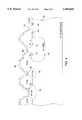
- FIGS. 3 and 4an illustrative embodiment of the two-transistor, zero-power, electrically-alterable non-volatile latch element 10 of the present invention as embodied in semiconductor material is shown.
- FIG. 3is a top view of an illustrative semiconductor layout of the two-transistor, zero-power, electrically-alterable non-volatile latch element 10 of FIG. 1.
- FIG. 4is a cross-sectional view of the illustrative semiconductor layout of the two-transistor, zero-power, electrically-alterable non-volatile latch element of FIG. 3, taken through lines 4--4.
- the P-Channel MOS transistor 12 of FIG. 1is disposed in n-well 40 and its source and drain comprise p+ diffused regions 42 and 44, respectively.
- the N-Channel MOS transistor 14 of FIG. 1is disposed in the p-type semiconductor substrate 46 (more easily seen in FIG. 4) and its drain and source regions comprise n+ diffused regions 48 and 50, respectively.
- Metal strip 52is used to connect p+ diffused region 44 to n+ diffused region 48 via contacts 54 and 56.
- Vcc metal line 58is connected to p+ diffusion region 42 via contacts 60 and ground metal line 62 is connected to n+diffusion region 50 via contacts 64.
- Floating gate 24 of FIG. 1is formed from a single layer of polysilicon 66 having extending finger 68 disposed above the channel region between p+ diffused regions 42 and 44 forming the floating gate portion of P-Channel MOS transistor 12.
- a second extending finger 70is disposed above the channel region between n+ diffused regions 48 and 50 forming the floating gate portion of N-Channel MOS transistor 14.
- the source and drain diffusions 42 and 44, and 48 and 50 for both the P-Channel and N-Channel MOS transistors 12 and 14may be formed using self-aligned gate techniques as are known in the art.
- the common control gate node 28 of P-Channel MOS transistor 12 and N-Channel MOS transistor 14may be formed as a high-voltage n-type diffused region 72 in the p-type semiconductor substrate 46.
- High-voltage n-type diffused region 72should be formed so as to withstand the contemplated Vpp voltage with an appropriate margin as is well understood in the art.
- the high-voltage n-type diffused region 72is capacitively coupled to an enlarged portion of the overlying single layer of polysilicon 66 to enhance capacitive coupling.
- a dielectric layer 74typically formed from high quality oxide as is known in the art, to a thickness of from about 50 to about 130 angstroms, preferably about 80 angstroms, separates the high-voltage n-type diffused region 72 from the single layer of polysilicon 66 and forms coupling capacitor 76.
- the area of a typical coupling capacitor 76is about 7 to 10 times the area of the tunneling capacitor.
- the erase gate node 26 of two-transistor, zero-power, electrically-alterable non-volatile latch element 10 of FIG. 1is formed as a high-voltage n-type diffused region 78 in the p-type semiconductor substrate 46.
- high-voltage n-type diffused region 78should also be formed so as to withstand the contemplated Vpp voltage with an appropriate margin as is well understood in the art.
- a tunneling capacitor 80is formed by the intersection of the high-voltage n-type diffused region 78 with the overlying single layer of polysilicon 66.
- the single layer of polysilicon 66is separated from the high voltage n-type diffused region 78 by a tunneling dielectric layer 82 typically formed from high quality oxide as is known in the art, to a thickness of about 50 to about 130 angstroms, preferably about 80 angstroms.
- the area of a typical tunneling capacitor 80is about the smallest feature size which can be printed using photolithography techniques, or may be formed by an overlap of the source/drain diffusion with the polysilicon floating gate.
- FIGS. 3 and 4employs "gate" elements which are actually disposed in the substrate, high voltage n-type diffused regions 72 and 78 could easily be replaced by polysilicon lines formed in a second layer of polysilicon as is well-known in the EPROM and EEPROM art.
- Such structuresare equivalent to the structures depicted in the figures herein and are thus intended to fall within the scope of the present invention.
- the two-transistor, zero-power, electrically-alterable non-volatile latch elements 10may be programmed and erased by a Vpp voltage in the range of about 10 to about 15 volts.
- the two-transistor, zero-power, electrically-alterable non-volatile latch element 10 of the present inventionmay be fabricated as a part of a conventional single-level polysilicon gate CMOS integrated circuit fabrication process. Such a process begins with the conventional steps for forming the n-wells, the field implant and field oxidation steps.
- the high-voltage n-type diffused regions 78 and 72 comprising the erase gate and control gate nodes 26 and 28are then formed in the p-type semiconductor substrate 46 using buried n+ mask and implant.
- the erase gate node 26can also be formed in the n-type source/drain diffusion using known high-voltage techniques.
- a tunnel windowis etched to expose the high-voltage n-type diffused region 78 comprising the global erase gate node 26 and the tunneling dielectric layer 82 is formed, preferably from high quality oxide, and is then defined in the tunnel window.
- the single layer of polysilicon 66 which will comprise the floating gateis then formed, doped and defined, using conventional semiconductor processing technology.
- the gate oxide step for the formation of other P-Channel and N-Channel transistor devices on the integrated circuitis then performed, followed by deposition, doping, and definition of the polysilicon gates for those other transistor devices.
- the global erase and control gate node 26 and 28are to be formed from polysilicon layers, an inter-poly oxide is formed, windows are etched to expose regions of the floating gate, and the tunneling dielectric layer 82 and control gate capacitor dielectric layer 74 are formed prior to performing the gate poly deposition step.
- An implant oxideis formed, followed by the masking and implant steps necessary to form both the P-Channel and N-Channel self-aligned source and drain regions 42 and 44, and 48 and 50.
- FIG. 5Such an array 90 of two-transistor, zero-power, electrically-alterable non-volatile latch elements is shown in FIG. 5 in schematic form according to another aspect of the present invention.
- the array 90includes a plurality of two-transistor, zero-power, electrically-alterable non-volatile latch elements arranged in rows and columns.
- the two-transistor, zero-power, electrically-alterable non-volatile latch elementsare shown as squares and designated with reference numerals 10-1, 10-2 10-3, and 10-4.
- the illustrative array 90 of FIG. 5is shown comprising two rows and two columns, those of ordinary skill in the art will readily recognize that the array of FIG. 5 is for purposes of illustration and that much larger arrays are practical according to the present invention.
- Two-transistor, zero-power, electrically-alterable non-volatile latch elements 10-1 and 10-2form the first row of array 90 and two-transistor, zero-power, electrically-alterable non-volatile latch elements 10-3 and 10-4 form the second row of array 90.
- two-transistor, zero-power, electrically-alterable non-volatile latch elements 10-1 and 10-3form the first column of array 90 and two-transistor, zero-power, electrically-alterable non-volatile latch elements 10-2 and 10-4 form the second column of array 90.
- Each two-transistor, zero-power, electrically-alterable non-volatile latch element 10-1 through 10-4has associated with it a pass transistor.
- These pass transistorsare labelled with reference numerals 92-1 through 92-4, the numeric suffixes corresponding to the numeric suffixes of the two-transistor, zero-power, electrically-alterable non-volatile latch element 10-1 through 10-4 with which each pass transistor 92-1 through 92-4 is associated.
- the gate of each pass transistor 92-1 through 92-4is connected to the output node of its associated two-transistor, zero-power, electrically-alterable non-volatile latch element 10-1 through 10-4.
- pass transistors 92-1 through 92-4are shown as N-Channel MOS transistors, but those of ordinary skill in the art will recognize that other types of devices may be used for different applications without departing from the principles of the present invention.
- the individual two-transistor, zero-power, electrically-alterable non-volatile latch elements 10-1 through 10-4 in the array 90 of the present inventionmay be addressed and programmed or may be erased.
- a global erase modeis provided, although those of ordinary skill in the art will easily understand how to configure an array in which the two-transistor, zero-power, electrically-alterable non-volatile latch elements 10-1 through 10-4 could be individually erased.
- select transistors 94-1 through 94-4are used to select the individual two-transistor, zero-power, electrically-alterable non-volatile latch elements 10-1 through 10-4 for programming.
- the numeric suffixes of the select transistors 94-1 through 94-4 in FIG. 5correspond to the numeric suffixes of the two-transistor, zero-power, electrically-alterable non-volatile latch element 10-1 through 10-4 with which each pass transistor 92-1 through 92-4 is associated.
- the select transistors 94-1 through 94-4are used to deliver the programming voltage to selected ones of the two-transistor, zero-power, electrically-alterable non-volatile latch elements 10-1 through 10-4 to program them.
- select transistors 94-1 and 94-2are connected to a first row line 96.
- the gates of select transistors 94-3 and 94-4are connected to a second row line 98.
- the drains of select transistors 94-1 and 94-3are connected to a first column line 100.
- the drains of select transistors 94-2 and 94-4are connected to a second column line 102.
- the source of each of the select transistors 94-1 through 94-4is connected to the input node (the common control gate node 28) of its corresponding two-transistor, zero-power, electrically-alterable non-volatile latch element 10-1 through 10-4.
- Global erase line 104is shown connected to each of the two-transistor, zero-power, electrically-alterable non-volatile latch element 10-1 through 10-4.
- the global erase line 104is connected to the erase gate node 26 of each of the two-transistor, zero-power, electrically-alterable non-volatile latch elements 10-1 through 10-4 and is used to erase or reset all of the two-transistor, zero-power, electrically-alterable non-volatile latch elements 10-1 through 10-4 simultaneously.
- the first and second row lines 96 and 98are kept at zero volts so that select transistors 94-1 through 94-4 are turned off.
- the first and second row lines 96 and 98 and the first and second column lines 100 and 102are used to select the two-transistor, zero-power, electrically-alterable non-volatile latch elements 10-1 through 10-4 to be programmed and to deliver them appropriate voltages to the selected two-transistor, zero-power, electrically-alterable non-volatile latch.
- any one or more of the two-transistor, zero-power, electrically-alterable non-volatile latch elements 10-1 through 10-4may be programmed.
- second row line 98is brought to Vpp while first row line 96 is kept grounded.
- Vppis also placed on first column line 100 while second column line 102 is kept grounded.
- the global erase line 104is also kept grounded.
- This actionturns on select transistor 94-3, placing Vpp on the common control gate node 28 of the N-Channel and P-Channel MOS transistors in two-transistor, zero-power, electrically-alterable non-volatile latch element 10-3.
- first row line 96is held at ground, both select transistors 94-1 and 94-2 are turned off. Because second column line 102 is held at ground, Vpp does not appear at the control gate node 28 of the transistors in two-transistor, zero-power, electrically-alterable non-volatile latch element 10-4 even though the gate of select transistor 94-4 is at a voltage which would turn it on if there was any voltage at its drain. Thus, no tunneling of electrons will occur onto the floating gates of two-transistor, zero-power, electrically-alterable non-volatile latch elements 10-1, 10-2, and 10-4.
- the driving of the various voltages onto first and second row lines, first and second column lines and global erase line 96, 98, 100, 102, and 104, respectively,is provided by programming circuitry 106.
- Circuitry for generating and switching the necessary voltages for programming the devices of the present inventionis well known in the art and is a matter of simple design choice.
- the voltagesmay be generated on-chip by charge pumps as is known in the art or may be supplied from off chip via selected I/O pins as is well known in the art.
- the two-transistor, zero-power, electrically-alterable non-volatile latch element 10 of the present inventionwill always power up to a desired state once it has been pre-programmed. Unlike some of the prior art latch elements, it employs independent read and write paths, thus minimizing the read disturb problem. It does not require high-voltage n-well technology. It employs a small cell size, making it an excellent candidate for array applications, and enjoys excellent long-term data retention.
Landscapes
- Non-Volatile Memory (AREA)
- Read Only Memory (AREA)
- Semiconductor Memories (AREA)
- Logic Circuits (AREA)
Abstract
Description
Claims (3)
Priority Applications (5)
| Application Number | Priority Date | Filing Date | Title |
|---|---|---|---|
| US08/369,760US5587603A (en) | 1995-01-06 | 1995-01-06 | Two-transistor zero-power electrically-alterable non-volatile latch |
| PCT/US1996/000306WO1996021273A2 (en) | 1995-01-06 | 1996-01-04 | Two-transistor zero-power electrically-alterable non-volatile latch |
| CA002198359ACA2198359A1 (en) | 1995-01-06 | 1996-01-04 | Two-transistor zero-power electrically-alterable non-volatile latch |
| JP8521270AJPH10510124A (en) | 1995-01-06 | 1996-01-04 | Two-transistor power-saving electrically rewritable nonvolatile latch element |
| EP96907003AEP0801844A2 (en) | 1995-01-06 | 1996-01-04 | Two-transistor zero-power electrically-alterable non-volatile latch |
Applications Claiming Priority (1)
| Application Number | Priority Date | Filing Date | Title |
|---|---|---|---|
| US08/369,760US5587603A (en) | 1995-01-06 | 1995-01-06 | Two-transistor zero-power electrically-alterable non-volatile latch |
Publications (1)
| Publication Number | Publication Date |
|---|---|
| US5587603Atrue US5587603A (en) | 1996-12-24 |
Family
ID=23456803
Family Applications (1)
| Application Number | Title | Priority Date | Filing Date |
|---|---|---|---|
| US08/369,760Expired - LifetimeUS5587603A (en) | 1995-01-06 | 1995-01-06 | Two-transistor zero-power electrically-alterable non-volatile latch |
Country Status (5)
| Country | Link |
|---|---|
| US (1) | US5587603A (en) |
| EP (1) | EP0801844A2 (en) |
| JP (1) | JPH10510124A (en) |
| CA (1) | CA2198359A1 (en) |
| WO (1) | WO1996021273A2 (en) |
Cited By (73)
| Publication number | Priority date | Publication date | Assignee | Title |
|---|---|---|---|---|
| US5886377A (en)* | 1996-03-07 | 1999-03-23 | Rohm Co., Ltd. | Semiconductor device and a method for manufacturing thereof |
| US6014044A (en)* | 1996-10-30 | 2000-01-11 | Stmicroelectronics S.R.L. | Voltage comparator with floating gate MOS transistor |
| US6100560A (en)* | 1999-03-26 | 2000-08-08 | Cypress Semiconductor Corp. | Nonvolatile cell |
| US6144580A (en)* | 1998-12-11 | 2000-11-07 | Cypress Semiconductor Corp. | Non-volatile inverter latch |
| US6307773B1 (en) | 2000-07-28 | 2001-10-23 | National Semiconductor Corporation | Non-volatile latch with program strength verification |
| US6356478B1 (en)* | 2000-12-21 | 2002-03-12 | Actel Corporation | Flash based control for field programmable gate array |
| US20030063518A1 (en)* | 2001-09-18 | 2003-04-03 | David Fong | Programming methods and circuits for semiconductor memory cell and memory array using a breakdown phenomena in an ultra-thin dielectric |
| US20030071296A1 (en)* | 2001-10-17 | 2003-04-17 | Peng Jack Zezhong | Reprogrammable non-volatile memory using a breakdown phenomena in an ultra-thin dielectric |
| US20030198085A1 (en)* | 2001-09-18 | 2003-10-23 | Peng Jack Zezhong | Semiconductor memory cell and memory array using a breakdown phenomena in an ultra-thin dielectric |
| US6639840B1 (en) | 2002-01-03 | 2003-10-28 | Fairchild Semiconductor Corporation | Non-volatile latch circuit that has minimal control circuitry |
| US20030202376A1 (en)* | 2002-04-26 | 2003-10-30 | Peng Jack Zezhong | High density semiconductor memory cell and memory array using a single transistor |
| US6650143B1 (en) | 2002-07-08 | 2003-11-18 | Kilopass Technologies, Inc. | Field programmable gate array based upon transistor gate oxide breakdown |
| US20040031853A1 (en)* | 2001-10-17 | 2004-02-19 | Peng Jack Zezhong | Smart card having memory using a breakdown phenomena in an ultra-thin dielectric |
| US20040125671A1 (en)* | 2002-04-26 | 2004-07-01 | Peng Jack Zezhong | High density semiconductor memory cell and memory array using a single transistor having a buried N+ connection |
| US20040156234A1 (en)* | 2002-04-26 | 2004-08-12 | Peng Jack Zezhong | High density semiconductor memory cell and memory array using a single transistor and having variable gate oxide breakdown |
| US6791891B1 (en) | 2003-04-02 | 2004-09-14 | Kilopass Technologies, Inc. | Method of testing the thin oxide of a semiconductor memory cell that uses breakdown voltage |
| US20040208055A1 (en)* | 2002-09-26 | 2004-10-21 | Jianguo Wang | Methods and circuits for testing programmability of a semiconductor memory cell and memory array using a breakdown phenomenon in an ultra-thin dielectric |
| US20040223363A1 (en)* | 2002-04-26 | 2004-11-11 | Peng Jack Zezhong | High density semiconductor memory cell and memory array using a single transistor and having counter-doped poly and buried diffusion wordline |
| US20040223370A1 (en)* | 2002-09-26 | 2004-11-11 | Jianguo Wang | Methods and circuits for programming of a semiconductor memory cell and memory array using a breakdown phenomenon in an ultra-thin dielectric |
| US20040233736A1 (en)* | 2003-04-10 | 2004-11-25 | Stmicroelectronics S.R.L. | Nonvolatile switch, in particular for high-density nonvolatile programmable-logic devices |
| US20050035783A1 (en)* | 2003-08-15 | 2005-02-17 | Man Wang | Field programmable gate array |
| US20050169040A1 (en)* | 2004-02-03 | 2005-08-04 | Peng Jack Z. | Combination field programmable gate array allowing dynamic reprogrammability |
| US20050169039A1 (en)* | 2004-02-03 | 2005-08-04 | Peng Jack Z. | Combination field programmable gate array allowing dynamic reprogrammability and non-volatile programmability based upon transistor gate oxide breakdown |
| US7099189B1 (en) | 2004-10-05 | 2006-08-29 | Actel Corporation | SRAM cell controlled by non-volatile memory cell |
| US20060232296A1 (en)* | 2005-04-18 | 2006-10-19 | Kilopass Technologies, Inc. | Fast processing path using field programmable gate array logic unit |
| US7135886B2 (en) | 2004-09-20 | 2006-11-14 | Klp International, Ltd. | Field programmable gate arrays using both volatile and nonvolatile memory cell properties and their control |
| US20060284238A1 (en)* | 2005-06-15 | 2006-12-21 | Actel Corporation | Non-volatile two-transistor programmable logic cell and array layout |
| US7164290B2 (en) | 2004-06-10 | 2007-01-16 | Klp International, Ltd. | Field programmable gate array logic unit and its cluster |
| US20080101117A1 (en)* | 2006-11-01 | 2008-05-01 | Gumbo Logic, Inc. | Trap-charge non-volatile switch connector for programmable logic |
| US20080169498A1 (en)* | 2005-06-13 | 2008-07-17 | Actel Corporation | Non-volatile programmable memory cell and array for programmable logic array |
| US20080219052A1 (en)* | 2007-03-05 | 2008-09-11 | Kucic Matthew R | Always-evaluated zero standby-current programmable non-volatile memory |
| US20080246098A1 (en)* | 2004-05-06 | 2008-10-09 | Sidense Corp. | Split-channel antifuse array architecture |
| US7538382B1 (en) | 2005-06-15 | 2009-05-26 | Actel Corporation | Non-volatile two-transistor programmable logic cell and array layout |
| US20100149873A1 (en)* | 2008-12-12 | 2010-06-17 | Actel Corporation | Push-pull fpga cell |
| US20100157688A1 (en)* | 2008-12-23 | 2010-06-24 | Actel Corporation | Push-pull memory cell configured for simultaneous programming of n-channel and p-channel non-volatile transistors |
| US7768056B1 (en) | 2005-06-13 | 2010-08-03 | Actel Corporation | Isolated-nitride-region non-volatile memory cell and fabrication method |
| US20100208520A1 (en)* | 2009-02-13 | 2010-08-19 | Actel Corporation | Array and control method for flash based fpga cell |
| US20100244115A1 (en)* | 2004-05-06 | 2010-09-30 | Sidense Corporation | Anti-fuse memory cell |
| US7816947B1 (en)* | 2008-03-31 | 2010-10-19 | Man Wang | Method and apparatus for providing a non-volatile programmable transistor |
| US7835179B1 (en) | 2007-09-20 | 2010-11-16 | Venkatraman Prabhakar | Non-volatile latch with low voltage operation |
| US7859240B1 (en) | 2007-05-22 | 2010-12-28 | Cypress Semiconductor Corporation | Circuit and method for preventing reverse current flow into a voltage regulator from an output thereof |
| US20110002167A1 (en)* | 2009-07-02 | 2011-01-06 | Actel Corporation | Push-pull programmable logic device cell |
| US20120236635A1 (en)* | 2010-06-17 | 2012-09-20 | Ching Wen-Hao | Logic-Based Multiple Time Programming Memory Cell |
| US8735297B2 (en) | 2004-05-06 | 2014-05-27 | Sidense Corporation | Reverse optical proximity correction method |
| US8829594B2 (en) | 2011-11-30 | 2014-09-09 | Kabushiki Kaisha Toshiba | Nonvolatile programmable switches |
| US8958245B2 (en) | 2010-06-17 | 2015-02-17 | Ememory Technology Inc. | Logic-based multiple time programming memory cell compatible with generic CMOS processes |
| US9042174B2 (en) | 2010-06-17 | 2015-05-26 | Ememory Technology Inc. | Non-volatile memory cell |
| US9123572B2 (en) | 2004-05-06 | 2015-09-01 | Sidense Corporation | Anti-fuse memory cell |
| KR20170034216A (en)* | 2015-09-18 | 2017-03-28 | 삼성전자주식회사 | Non-volatile inverter |
| US10128852B2 (en) | 2015-12-17 | 2018-11-13 | Microsemi SoC Corporation | Low leakage ReRAM FPGA configuration cell |
| US10147485B2 (en) | 2016-09-29 | 2018-12-04 | Microsemi Soc Corp. | Circuits and methods for preventing over-programming of ReRAM-based memory cells |
| US10447274B2 (en)* | 2017-07-11 | 2019-10-15 | iCometrue Company Ltd. | Logic drive based on standard commodity FPGA IC chips using non-volatile memory cells |
| US10489544B2 (en) | 2016-12-14 | 2019-11-26 | iCometrue Company Ltd. | Logic drive based on standard commodity FPGA IC chips |
| US10522224B2 (en) | 2017-08-11 | 2019-12-31 | Microsemi Soc Corp. | Circuitry and methods for programming resistive random access memory devices |
| US10523210B2 (en) | 2018-02-01 | 2019-12-31 | iCometrue Company Ltd. | Logic drive using standard commodity programmable logic IC chips comprising non-volatile random access memory cells |
| US10546633B2 (en) | 2016-12-09 | 2020-01-28 | Microsemi Soc Corp. | Resistive random access memory cell |
| US10608638B2 (en) | 2018-05-24 | 2020-03-31 | iCometrue Company Ltd. | Logic drive using standard commodity programmable logic IC chips |
| US10623000B2 (en) | 2018-02-14 | 2020-04-14 | iCometrue Company Ltd. | Logic drive using standard commodity programmable logic IC chips |
| US10630296B2 (en) | 2017-09-12 | 2020-04-21 | iCometrue Company Ltd. | Logic drive with brain-like elasticity and integrality based on standard commodity FPGA IC chips using non-volatile memory cells |
| US10892011B2 (en) | 2018-09-11 | 2021-01-12 | iCometrue Company Ltd. | Logic drive using standard commodity programmable logic IC chips comprising non-volatile random access memory cells |
| US10937762B2 (en) | 2018-10-04 | 2021-03-02 | iCometrue Company Ltd. | Logic drive based on multichip package using interconnection bridge |
| US10957679B2 (en) | 2017-08-08 | 2021-03-23 | iCometrue Company Ltd. | Logic drive based on standardized commodity programmable logic semiconductor IC chips |
| US10985154B2 (en) | 2019-07-02 | 2021-04-20 | iCometrue Company Ltd. | Logic drive based on multichip package comprising standard commodity FPGA IC chip with cryptography circuits |
| US11211334B2 (en) | 2018-11-18 | 2021-12-28 | iCometrue Company Ltd. | Logic drive based on chip scale package comprising standardized commodity programmable logic IC chip and memory IC chip |
| US11227838B2 (en) | 2019-07-02 | 2022-01-18 | iCometrue Company Ltd. | Logic drive based on multichip package comprising standard commodity FPGA IC chip with cooperating or supporting circuits |
| US11309334B2 (en) | 2018-09-11 | 2022-04-19 | iCometrue Company Ltd. | Logic drive using standard commodity programmable logic IC chips comprising non-volatile random access memory cells |
| US11600526B2 (en) | 2020-01-22 | 2023-03-07 | iCometrue Company Ltd. | Chip package based on through-silicon-via connector and silicon interconnection bridge |
| US11616046B2 (en) | 2018-11-02 | 2023-03-28 | iCometrue Company Ltd. | Logic drive based on chip scale package comprising standardized commodity programmable logic IC chip and memory IC chip |
| US11625523B2 (en) | 2016-12-14 | 2023-04-11 | iCometrue Company Ltd. | Logic drive based on standard commodity FPGA IC chips |
| US11637056B2 (en) | 2019-09-20 | 2023-04-25 | iCometrue Company Ltd. | 3D chip package based on through-silicon-via interconnection elevator |
| US11887930B2 (en) | 2019-08-05 | 2024-01-30 | iCometrue Company Ltd. | Vertical interconnect elevator based on through silicon vias |
| US12176278B2 (en) | 2021-05-30 | 2024-12-24 | iCometrue Company Ltd. | 3D chip package based on vertical-through-via connector |
| US12268012B2 (en) | 2021-09-24 | 2025-04-01 | iCometrue Company Ltd. | Multi-output look-up table (LUT) for use in coarse-grained field-programmable-gate-array (FPGA) integrated-circuit (IC) chip |
Families Citing this family (4)
| Publication number | Priority date | Publication date | Assignee | Title |
|---|---|---|---|---|
| US6404006B2 (en)* | 1998-12-01 | 2002-06-11 | Vantis Corporation | EEPROM cell with tunneling across entire separated channels |
| US6294810B1 (en) | 1998-12-22 | 2001-09-25 | Vantis Corporation | EEPROM cell with tunneling at separate edge and channel regions |
| US6294811B1 (en) | 1999-02-05 | 2001-09-25 | Vantis Corporation | Two transistor EEPROM cell |
| US6172392B1 (en) | 1999-03-29 | 2001-01-09 | Vantis Corporation | Boron doped silicon capacitor plate |
Citations (15)
| Publication number | Priority date | Publication date | Assignee | Title |
|---|---|---|---|---|
| EP0053878A2 (en)* | 1980-12-08 | 1982-06-16 | Kabushiki Kaisha Toshiba | Semiconductor memory device |
| US4375086A (en)* | 1980-05-15 | 1983-02-22 | Ncr Corporation | Volatile/non-volatile dynamic RAM system |
| US4495427A (en)* | 1980-12-05 | 1985-01-22 | Rca Corporation | Programmable logic gates and networks |
| US4617479A (en)* | 1984-05-03 | 1986-10-14 | Altera Corporation | Programmable logic array device using EPROM technology |
| US4622656A (en)* | 1982-12-16 | 1986-11-11 | Seiko Instruments & Electronics Ltd. | Non-volatile semiconductor memory |
| US4742492A (en)* | 1985-09-27 | 1988-05-03 | Texas Instruments Incorporated | EEPROM memory cell having improved breakdown characteristics and driving circuitry therefor |
| US4822753A (en)* | 1988-05-09 | 1989-04-18 | Motorola, Inc. | Method for making a w/tin contact |
| US4829203A (en)* | 1988-04-20 | 1989-05-09 | Texas Instruments Incorporated | Integrated programmable bit circuit with minimal power requirement |
| US4851361A (en)* | 1988-02-04 | 1989-07-25 | Atmel Corporation | Fabrication process for EEPROMS with high voltage transistors |
| US4878199A (en)* | 1987-02-27 | 1989-10-31 | Kabushiki Kaisha Toshiba | Semiconductor memory device |
| US4885719A (en)* | 1987-08-19 | 1989-12-05 | Ict International Cmos Technology, Inc. | Improved logic cell array using CMOS E2 PROM cells |
| EP0515039A2 (en)* | 1991-05-10 | 1992-11-25 | Altera Corporation | A complementary low power non-volatile reconfigurable eecell |
| US5247478A (en)* | 1992-03-06 | 1993-09-21 | Altera Corporation | Programmable transfer-devices |
| US5380672A (en)* | 1990-12-18 | 1995-01-10 | Sundisk Corporation | Dense vertical programmable read only memory cell structures and processes for making them |
| US5424985A (en)* | 1993-06-30 | 1995-06-13 | Sgs-Thomson Microelectronics, Inc. | Compensating delay element for clock generation in a memory device |
- 1995
- 1995-01-06USUS08/369,760patent/US5587603A/ennot_activeExpired - Lifetime
- 1996
- 1996-01-04CACA002198359Apatent/CA2198359A1/ennot_activeAbandoned
- 1996-01-04WOPCT/US1996/000306patent/WO1996021273A2/ennot_activeApplication Discontinuation
- 1996-01-04JPJP8521270Apatent/JPH10510124A/enactivePending
- 1996-01-04EPEP96907003Apatent/EP0801844A2/ennot_activeWithdrawn
Patent Citations (16)
| Publication number | Priority date | Publication date | Assignee | Title |
|---|---|---|---|---|
| US4375086A (en)* | 1980-05-15 | 1983-02-22 | Ncr Corporation | Volatile/non-volatile dynamic RAM system |
| US4495427A (en)* | 1980-12-05 | 1985-01-22 | Rca Corporation | Programmable logic gates and networks |
| EP0053878A2 (en)* | 1980-12-08 | 1982-06-16 | Kabushiki Kaisha Toshiba | Semiconductor memory device |
| US4622656A (en)* | 1982-12-16 | 1986-11-11 | Seiko Instruments & Electronics Ltd. | Non-volatile semiconductor memory |
| US4617479B1 (en)* | 1984-05-03 | 1993-09-21 | Altera Semiconductor Corp. | Programmable logic array device using eprom technology |
| US4617479A (en)* | 1984-05-03 | 1986-10-14 | Altera Corporation | Programmable logic array device using EPROM technology |
| US4742492A (en)* | 1985-09-27 | 1988-05-03 | Texas Instruments Incorporated | EEPROM memory cell having improved breakdown characteristics and driving circuitry therefor |
| US4878199A (en)* | 1987-02-27 | 1989-10-31 | Kabushiki Kaisha Toshiba | Semiconductor memory device |
| US4885719A (en)* | 1987-08-19 | 1989-12-05 | Ict International Cmos Technology, Inc. | Improved logic cell array using CMOS E2 PROM cells |
| US4851361A (en)* | 1988-02-04 | 1989-07-25 | Atmel Corporation | Fabrication process for EEPROMS with high voltage transistors |
| US4829203A (en)* | 1988-04-20 | 1989-05-09 | Texas Instruments Incorporated | Integrated programmable bit circuit with minimal power requirement |
| US4822753A (en)* | 1988-05-09 | 1989-04-18 | Motorola, Inc. | Method for making a w/tin contact |
| US5380672A (en)* | 1990-12-18 | 1995-01-10 | Sundisk Corporation | Dense vertical programmable read only memory cell structures and processes for making them |
| EP0515039A2 (en)* | 1991-05-10 | 1992-11-25 | Altera Corporation | A complementary low power non-volatile reconfigurable eecell |
| US5247478A (en)* | 1992-03-06 | 1993-09-21 | Altera Corporation | Programmable transfer-devices |
| US5424985A (en)* | 1993-06-30 | 1995-06-13 | Sgs-Thomson Microelectronics, Inc. | Compensating delay element for clock generation in a memory device |
Cited By (186)
| Publication number | Priority date | Publication date | Assignee | Title |
|---|---|---|---|---|
| US5886377A (en)* | 1996-03-07 | 1999-03-23 | Rohm Co., Ltd. | Semiconductor device and a method for manufacturing thereof |
| US6130130A (en)* | 1996-03-07 | 2000-10-10 | Rohm Co., Ltd. | Semiconductor device and a method for manufacturing thereof |
| US6014044A (en)* | 1996-10-30 | 2000-01-11 | Stmicroelectronics S.R.L. | Voltage comparator with floating gate MOS transistor |
| US6144580A (en)* | 1998-12-11 | 2000-11-07 | Cypress Semiconductor Corp. | Non-volatile inverter latch |
| US6349055B1 (en) | 1998-12-11 | 2002-02-19 | Cypress Semiconductor Corp. | Non-volatile inverter latch |
| US6100560A (en)* | 1999-03-26 | 2000-08-08 | Cypress Semiconductor Corp. | Nonvolatile cell |
| US6307773B1 (en) | 2000-07-28 | 2001-10-23 | National Semiconductor Corporation | Non-volatile latch with program strength verification |
| US6445631B2 (en) | 2000-07-28 | 2002-09-03 | National Semiconductor Corporation | Non-volatile latch with program strength verification |
| US6356478B1 (en)* | 2000-12-21 | 2002-03-12 | Actel Corporation | Flash based control for field programmable gate array |
| US6822888B2 (en) | 2001-09-18 | 2004-11-23 | Kilopass Technologies, Inc. | Semiconductor memory cell and memory array using a breakdown phenomena in an ultra-thin dielectric |
| US20030198085A1 (en)* | 2001-09-18 | 2003-10-23 | Peng Jack Zezhong | Semiconductor memory cell and memory array using a breakdown phenomena in an ultra-thin dielectric |
| US20030063518A1 (en)* | 2001-09-18 | 2003-04-03 | David Fong | Programming methods and circuits for semiconductor memory cell and memory array using a breakdown phenomena in an ultra-thin dielectric |
| US6798693B2 (en) | 2001-09-18 | 2004-09-28 | Kilopass Technologies, Inc. | Semiconductor memory cell and memory array using a breakdown phenomena in an ultra-thin dielectric |
| US6667902B2 (en) | 2001-09-18 | 2003-12-23 | Kilopass Technologies, Inc. | Semiconductor memory cell and memory array using a breakdown phenomena in an ultra-thin dielectric |
| US6671040B2 (en) | 2001-09-18 | 2003-12-30 | Kilopass Technologies, Inc. | Programming methods and circuits for semiconductor memory cell and memory array using a breakdown phenomena in an ultra-thin dielectric |
| US20040008538A1 (en)* | 2001-09-18 | 2004-01-15 | Peng Jack Zezhong | Semiconductor memory cell and memory array using a breakdown phenomena in an ultra-thin dielectric |
| US20040047218A1 (en)* | 2001-09-18 | 2004-03-11 | Kilopass Technologies, Inc. | Semiconductor memory cell and memory array using a breakdown phenomena in an ultra-thin dielectric |
| US20030071296A1 (en)* | 2001-10-17 | 2003-04-17 | Peng Jack Zezhong | Reprogrammable non-volatile memory using a breakdown phenomena in an ultra-thin dielectric |
| US20030071315A1 (en)* | 2001-10-17 | 2003-04-17 | Jack Zezhong Peng | Reprogrammable non-volatile memory using a breakdown phenomena in an ultra-thin dielectric |
| US6766960B2 (en) | 2001-10-17 | 2004-07-27 | Kilopass Technologies, Inc. | Smart card having memory using a breakdown phenomena in an ultra-thin dielectric |
| US20040031853A1 (en)* | 2001-10-17 | 2004-02-19 | Peng Jack Zezhong | Smart card having memory using a breakdown phenomena in an ultra-thin dielectric |
| US6639840B1 (en) | 2002-01-03 | 2003-10-28 | Fairchild Semiconductor Corporation | Non-volatile latch circuit that has minimal control circuitry |
| US20040223363A1 (en)* | 2002-04-26 | 2004-11-11 | Peng Jack Zezhong | High density semiconductor memory cell and memory array using a single transistor and having counter-doped poly and buried diffusion wordline |
| US6856540B2 (en) | 2002-04-26 | 2005-02-15 | Kilopass Technologies, Inc. | High density semiconductor memory cell and memory array using a single transistor |
| US20040156234A1 (en)* | 2002-04-26 | 2004-08-12 | Peng Jack Zezhong | High density semiconductor memory cell and memory array using a single transistor and having variable gate oxide breakdown |
| US6777757B2 (en) | 2002-04-26 | 2004-08-17 | Kilopass Technologies, Inc. | High density semiconductor memory cell and memory array using a single transistor |
| US6992925B2 (en) | 2002-04-26 | 2006-01-31 | Kilopass Technologies, Inc. | High density semiconductor memory cell and memory array using a single transistor and having counter-doped poly and buried diffusion wordline |
| US20040125671A1 (en)* | 2002-04-26 | 2004-07-01 | Peng Jack Zezhong | High density semiconductor memory cell and memory array using a single transistor having a buried N+ connection |
| US20030202376A1 (en)* | 2002-04-26 | 2003-10-30 | Peng Jack Zezhong | High density semiconductor memory cell and memory array using a single transistor |
| US6940751B2 (en) | 2002-04-26 | 2005-09-06 | Kilopass Technologies, Inc. | High density semiconductor memory cell and memory array using a single transistor and having variable gate oxide breakdown |
| US20030206467A1 (en)* | 2002-04-26 | 2003-11-06 | Peng Jack Zezhong | High density semiconductor memory cell and memory array using a single transistor |
| US6898116B2 (en) | 2002-04-26 | 2005-05-24 | Kilopass Technologies, Inc. | High density semiconductor memory cell and memory array using a single transistor having a buried N+ connection |
| US6650143B1 (en) | 2002-07-08 | 2003-11-18 | Kilopass Technologies, Inc. | Field programmable gate array based upon transistor gate oxide breakdown |
| US20040208055A1 (en)* | 2002-09-26 | 2004-10-21 | Jianguo Wang | Methods and circuits for testing programmability of a semiconductor memory cell and memory array using a breakdown phenomenon in an ultra-thin dielectric |
| US20040223370A1 (en)* | 2002-09-26 | 2004-11-11 | Jianguo Wang | Methods and circuits for programming of a semiconductor memory cell and memory array using a breakdown phenomenon in an ultra-thin dielectric |
| US7042772B2 (en) | 2002-09-26 | 2006-05-09 | Kilopass Technology, Inc. | Methods and circuits for programming of a semiconductor memory cell and memory array using a breakdown phenomenon in an ultra-thin dielectric |
| US7031209B2 (en) | 2002-09-26 | 2006-04-18 | Kilopass Technology, Inc. | Methods and circuits for testing programmability of a semiconductor memory cell and memory array using a breakdown phenomenon in an ultra-thin dielectric |
| US6791891B1 (en) | 2003-04-02 | 2004-09-14 | Kilopass Technologies, Inc. | Method of testing the thin oxide of a semiconductor memory cell that uses breakdown voltage |
| US20040233736A1 (en)* | 2003-04-10 | 2004-11-25 | Stmicroelectronics S.R.L. | Nonvolatile switch, in particular for high-density nonvolatile programmable-logic devices |
| US7088135B2 (en) | 2003-04-10 | 2006-08-08 | Stmicroelectronics S.R.L. | Nonvolatile switch, in particular for high-density nonvolatile programmable-logic devices |
| US20050035783A1 (en)* | 2003-08-15 | 2005-02-17 | Man Wang | Field programmable gate array |
| US6924664B2 (en) | 2003-08-15 | 2005-08-02 | Kilopass Technologies, Inc. | Field programmable gate array |
| US7061275B2 (en) | 2003-08-15 | 2006-06-13 | Klp International, Ltd. | Field programmable gate array |
| US20050184754A1 (en)* | 2003-08-15 | 2005-08-25 | Kilopass Technologies, Inc. | Field programmable gate array |
| US6977521B2 (en) | 2003-08-15 | 2005-12-20 | Klp International, Ltd. | Field programmable gate array |
| US6972986B2 (en) | 2004-02-03 | 2005-12-06 | Kilopass Technologies, Inc. | Combination field programmable gate array allowing dynamic reprogrammability and non-votatile programmability based upon transistor gate oxide breakdown |
| US20050169039A1 (en)* | 2004-02-03 | 2005-08-04 | Peng Jack Z. | Combination field programmable gate array allowing dynamic reprogrammability and non-volatile programmability based upon transistor gate oxide breakdown |
| US7064973B2 (en) | 2004-02-03 | 2006-06-20 | Klp International, Ltd. | Combination field programmable gate array allowing dynamic reprogrammability |
| US20050169040A1 (en)* | 2004-02-03 | 2005-08-04 | Peng Jack Z. | Combination field programmable gate array allowing dynamic reprogrammability |
| US8735297B2 (en) | 2004-05-06 | 2014-05-27 | Sidense Corporation | Reverse optical proximity correction method |
| US8313987B2 (en) | 2004-05-06 | 2012-11-20 | Sidense Corp. | Anti-fuse memory cell |
| US8026574B2 (en) | 2004-05-06 | 2011-09-27 | Sidense Corporation | Anti-fuse memory cell |
| US8283751B2 (en) | 2004-05-06 | 2012-10-09 | Sidense Corp. | Split-channel antifuse array architecture |
| US20080246098A1 (en)* | 2004-05-06 | 2008-10-09 | Sidense Corp. | Split-channel antifuse array architecture |
| US9123572B2 (en) | 2004-05-06 | 2015-09-01 | Sidense Corporation | Anti-fuse memory cell |
| US20100244115A1 (en)* | 2004-05-06 | 2010-09-30 | Sidense Corporation | Anti-fuse memory cell |
| US7164290B2 (en) | 2004-06-10 | 2007-01-16 | Klp International, Ltd. | Field programmable gate array logic unit and its cluster |
| US7135886B2 (en) | 2004-09-20 | 2006-11-14 | Klp International, Ltd. | Field programmable gate arrays using both volatile and nonvolatile memory cell properties and their control |
| US7099189B1 (en) | 2004-10-05 | 2006-08-29 | Actel Corporation | SRAM cell controlled by non-volatile memory cell |
| US7558112B2 (en) | 2004-10-05 | 2009-07-07 | Actel Corporation | SRAM cell controlled by flash memory cell |
| US20080266955A1 (en)* | 2004-10-05 | 2008-10-30 | Actel Corporation | Sram cell controlled by flash memory cell |
| US7193436B2 (en) | 2005-04-18 | 2007-03-20 | Klp International Ltd. | Fast processing path using field programmable gate array logic units |
| US20060232296A1 (en)* | 2005-04-18 | 2006-10-19 | Kilopass Technologies, Inc. | Fast processing path using field programmable gate array logic unit |
| US20080169498A1 (en)* | 2005-06-13 | 2008-07-17 | Actel Corporation | Non-volatile programmable memory cell and array for programmable logic array |
| US7910436B2 (en) | 2005-06-13 | 2011-03-22 | Actel Corporation | Isolated-nitride-region non-volatile memory cell and fabrication method |
| US20110018070A1 (en)* | 2005-06-13 | 2011-01-27 | Actel Corporation | Non-volatile programmable memory cell and array for programmable logic array |
| US9754948B2 (en) | 2005-06-13 | 2017-09-05 | Microsemi SoC Corporation | Non-volatile programmable memory cell and array for programmable logic array |
| US7838944B2 (en) | 2005-06-13 | 2010-11-23 | Actel Corporation | Non-volatile programmable memory cell and array for programmable logic array |
| US20100261326A1 (en)* | 2005-06-13 | 2010-10-14 | Actel Corporation | Isolated-nitride-region non-volatile memory cell and fabrication method |
| US7768056B1 (en) | 2005-06-13 | 2010-08-03 | Actel Corporation | Isolated-nitride-region non-volatile memory cell and fabrication method |
| US8633548B2 (en) | 2005-06-13 | 2014-01-21 | Microsemi SoC Corporation | Non-volatile programmable memory cell and array for programmable logic array |
| US20100038697A1 (en)* | 2005-06-15 | 2010-02-18 | Actel Corporation | Non-volatile two-transistor programmable logic cell and array layout |
| US7538379B1 (en) | 2005-06-15 | 2009-05-26 | Actel Corporation | Non-volatile two-transistor programmable logic cell and array layout |
| US7956404B2 (en) | 2005-06-15 | 2011-06-07 | Actel Corporation | Non-volatile two-transistor programmable logic cell and array layout |
| US7915665B2 (en) | 2005-06-15 | 2011-03-29 | Actel Corporation | Non-volatile two-transistor programmable logic cell and array layout |
| US7573093B1 (en) | 2005-06-15 | 2009-08-11 | Actel Corporation | Non-volatile two-transistor programmable logic cell and array layout |
| US7473960B1 (en) | 2005-06-15 | 2009-01-06 | Actel Corporation | Non-volatile two-transistor programmable logic cell and array layout |
| US7898018B2 (en) | 2005-06-15 | 2011-03-01 | Actel Corporation | Non-volatile two-transistor programmable logic cell and array layout |
| US20080093654A1 (en)* | 2005-06-15 | 2008-04-24 | Actel Corporation | Non-volatile two-transistor programmable logic cell and array layout |
| US20090159954A1 (en)* | 2005-06-15 | 2009-06-25 | Actel Corporation | Non-volatile two-transistor programmable logic cell and array layout |
| US20060284238A1 (en)* | 2005-06-15 | 2006-12-21 | Actel Corporation | Non-volatile two-transistor programmable logic cell and array layout |
| US7501681B2 (en) | 2005-06-15 | 2009-03-10 | Actel Corporation | Non-volatile two-transistor programmable logic cell and array layout |
| US20070215935A1 (en)* | 2005-06-15 | 2007-09-20 | Actel Corporation | Non-volatile two-transistor programmable logic cell and array layout |
| US7285818B2 (en) | 2005-06-15 | 2007-10-23 | Actel Corporation | Non-volatile two-transistor programmable logic cell and array layout |
| US7342278B2 (en) | 2005-06-15 | 2008-03-11 | Actel Corporation | Non-volatile two-transistor programmable logic cell and array layout |
| US7538382B1 (en) | 2005-06-15 | 2009-05-26 | Actel Corporation | Non-volatile two-transistor programmable logic cell and array layout |
| US8139410B2 (en) | 2006-11-01 | 2012-03-20 | Halo Lsi, Inc. | Trap-charge non-volatile switch connector for programmable logic |
| US20080101117A1 (en)* | 2006-11-01 | 2008-05-01 | Gumbo Logic, Inc. | Trap-charge non-volatile switch connector for programmable logic |
| US8023326B2 (en) | 2006-11-01 | 2011-09-20 | Halo Lsi, Inc. | Trap-charge non-volatile switch connector for programmable logic |
| US20100259981A1 (en)* | 2006-11-01 | 2010-10-14 | Gumbo Logic, Inc. | Trap-charge non-volatile switch connector for programmable logic |
| US7742336B2 (en) | 2006-11-01 | 2010-06-22 | Gumbo Logic, Inc. | Trap-charge non-volatile switch connector for programmable logic |
| US20100261324A1 (en)* | 2006-11-01 | 2010-10-14 | Gumbo Logic, Inc. | Trap-charge non-volatile switch connector for programmable logic |
| US20100259986A1 (en)* | 2006-11-01 | 2010-10-14 | Gumbo Logic, Inc. | Trap-charge non-volatile switch connector for programmable logic |
| US8027198B2 (en) | 2006-11-01 | 2011-09-27 | Halo Lsi, Inc. | Trap-charge non-volatile switch connector for programmable logic |
| US8089809B2 (en) | 2006-11-01 | 2012-01-03 | Halo Lsi, Inc. | Trap-charge non-volatile switch connector for programmable logic |
| US20100259985A1 (en)* | 2006-11-01 | 2010-10-14 | Gumbo Logic, Inc. | Trap-charge non-volatile switch connector for programmable logic |
| US7719895B2 (en)* | 2007-03-05 | 2010-05-18 | Gtronix, Inc. | Always-evaluated zero standby-current programmable non-volatile memory |
| US20080219052A1 (en)* | 2007-03-05 | 2008-09-11 | Kucic Matthew R | Always-evaluated zero standby-current programmable non-volatile memory |
| US7859240B1 (en) | 2007-05-22 | 2010-12-28 | Cypress Semiconductor Corporation | Circuit and method for preventing reverse current flow into a voltage regulator from an output thereof |
| US7835179B1 (en) | 2007-09-20 | 2010-11-16 | Venkatraman Prabhakar | Non-volatile latch with low voltage operation |
| US7816947B1 (en)* | 2008-03-31 | 2010-10-19 | Man Wang | Method and apparatus for providing a non-volatile programmable transistor |
| US20110024821A1 (en)* | 2008-12-12 | 2011-02-03 | Actel Corporation | Push-pull fpga cell |
| US7839681B2 (en) | 2008-12-12 | 2010-11-23 | Actel Corporation | Push-pull FPGA cell |
| US20100149873A1 (en)* | 2008-12-12 | 2010-06-17 | Actel Corporation | Push-pull fpga cell |
| US7929345B2 (en) | 2008-12-23 | 2011-04-19 | Actel Corporation | Push-pull memory cell configured for simultaneous programming of n-channel and p-channel non-volatile transistors |
| US20100157688A1 (en)* | 2008-12-23 | 2010-06-24 | Actel Corporation | Push-pull memory cell configured for simultaneous programming of n-channel and p-channel non-volatile transistors |
| US8120955B2 (en) | 2009-02-13 | 2012-02-21 | Actel Corporation | Array and control method for flash based FPGA cell |
| US20100208520A1 (en)* | 2009-02-13 | 2010-08-19 | Actel Corporation | Array and control method for flash based fpga cell |
| US20110001108A1 (en)* | 2009-07-02 | 2011-01-06 | Actel Corporation | Front to back resistive random access memory cells |
| US8981328B2 (en) | 2009-07-02 | 2015-03-17 | Microsemi SoC Corporation | Back to back resistive random access memory cells |
| US8269204B2 (en) | 2009-07-02 | 2012-09-18 | Actel Corporation | Back to back resistive random access memory cells |
| US8320178B2 (en) | 2009-07-02 | 2012-11-27 | Actel Corporation | Push-pull programmable logic device cell |
| US8415650B2 (en) | 2009-07-02 | 2013-04-09 | Actel Corporation | Front to back resistive random access memory cells |
| US10855286B2 (en) | 2009-07-02 | 2020-12-01 | Microsemi Soc Corp. | Front to back resistive random-access memory cells |
| US8269203B2 (en) | 2009-07-02 | 2012-09-18 | Actel Corporation | Resistive RAM devices for programmable logic devices |
| US8723151B2 (en) | 2009-07-02 | 2014-05-13 | Microsemi SoC Corporation | Front to back resistive random access memory cells |
| US20110001115A1 (en)* | 2009-07-02 | 2011-01-06 | Actel Corporation | Resistive ram devices for programmable logic devices |
| US10256822B2 (en) | 2009-07-02 | 2019-04-09 | Microsemi Soc Corp. | Front to back resistive random access memory cells |
| US9991894B2 (en) | 2009-07-02 | 2018-06-05 | Microsemi Soc Corp. | Resistive random access memory cells |
| US20110002167A1 (en)* | 2009-07-02 | 2011-01-06 | Actel Corporation | Push-pull programmable logic device cell |
| US20110001116A1 (en)* | 2009-07-02 | 2011-01-06 | Actel Corporation | Back to back resistive random access memory cells |
| US9042174B2 (en) | 2010-06-17 | 2015-05-26 | Ememory Technology Inc. | Non-volatile memory cell |
| US8958245B2 (en) | 2010-06-17 | 2015-02-17 | Ememory Technology Inc. | Logic-based multiple time programming memory cell compatible with generic CMOS processes |
| US20120236635A1 (en)* | 2010-06-17 | 2012-09-20 | Ching Wen-Hao | Logic-Based Multiple Time Programming Memory Cell |
| US8625350B2 (en)* | 2010-06-17 | 2014-01-07 | Ememory Technology Inc. | Logic-based multiple time programming memory cell |
| US8829594B2 (en) | 2011-11-30 | 2014-09-09 | Kabushiki Kaisha Toshiba | Nonvolatile programmable switches |
| KR20170034216A (en)* | 2015-09-18 | 2017-03-28 | 삼성전자주식회사 | Non-volatile inverter |
| US9747985B2 (en) | 2015-09-18 | 2017-08-29 | Samsung Electronics Co., Ltd. | Non-volatile inverter |
| US10128852B2 (en) | 2015-12-17 | 2018-11-13 | Microsemi SoC Corporation | Low leakage ReRAM FPGA configuration cell |
| US10270451B2 (en) | 2015-12-17 | 2019-04-23 | Microsemi SoC Corporation | Low leakage ReRAM FPGA configuration cell |
| US10147485B2 (en) | 2016-09-29 | 2018-12-04 | Microsemi Soc Corp. | Circuits and methods for preventing over-programming of ReRAM-based memory cells |
| US10546633B2 (en) | 2016-12-09 | 2020-01-28 | Microsemi Soc Corp. | Resistive random access memory cell |
| US10489544B2 (en) | 2016-12-14 | 2019-11-26 | iCometrue Company Ltd. | Logic drive based on standard commodity FPGA IC chips |
| US12153865B2 (en) | 2016-12-14 | 2024-11-26 | iCometrue Company Ltd. | Logic drive based on standard commodity FPGA IC chips |
| US11093677B2 (en) | 2016-12-14 | 2021-08-17 | iCometrue Company Ltd. | Logic drive based on standard commodity FPGA IC chips |
| US11625523B2 (en) | 2016-12-14 | 2023-04-11 | iCometrue Company Ltd. | Logic drive based on standard commodity FPGA IC chips |
| US11651132B2 (en) | 2016-12-14 | 2023-05-16 | iCometrue Company Ltd. | Logic drive based on standard commodity FPGA IC chips |
| US11264992B2 (en) | 2017-07-11 | 2022-03-01 | iCometrue Company Ltd. | Logic drive based on standard commodity FPGA IC chips using non-volatile memory cells |
| US12176901B2 (en) | 2017-07-11 | 2024-12-24 | iCometrue Company Ltd. | Logic drive based on standard commodity FPGA IC Chips using non-volatile memory cells |
| US10985760B2 (en) | 2017-07-11 | 2021-04-20 | iCometrue Company Ltd. | Logic drive based on standard commodity FPGA IC chips using non-volatile memory cells |
| US10594322B2 (en) | 2017-07-11 | 2020-03-17 | iCometrue Company Ltd. | Logic drive based on standard commodity FPGA IC chips using non-volatile memory cells |
| US10727837B2 (en) | 2017-07-11 | 2020-07-28 | iCometrue Company Ltd. | Logic drive based on standard commodity FPGA IC chips using non-volatile memory cells |
| US10447274B2 (en)* | 2017-07-11 | 2019-10-15 | iCometrue Company Ltd. | Logic drive based on standard commodity FPGA IC chips using non-volatile memory cells |
| US12368438B2 (en) | 2017-07-11 | 2025-07-22 | iCometrue Company Ltd. | Logic drive based on standard commodity FPGA IC chips using non-volatile memory cells |
| US12255195B2 (en) | 2017-08-08 | 2025-03-18 | iCometrue Company Ltd. | Logic drive based on standardized commodity programmable logic semiconductor IC chips |
| US10957679B2 (en) | 2017-08-08 | 2021-03-23 | iCometrue Company Ltd. | Logic drive based on standardized commodity programmable logic semiconductor IC chips |
| US11545477B2 (en) | 2017-08-08 | 2023-01-03 | iCometrue Company Ltd. | Logic drive based on standardized commodity programmable logic semiconductor IC chips |
| US10650890B2 (en) | 2017-08-11 | 2020-05-12 | Microsemi Soc Corp. | Circuitry and methods for programming resistive random access memory devices |
| US10522224B2 (en) | 2017-08-11 | 2019-12-31 | Microsemi Soc Corp. | Circuitry and methods for programming resistive random access memory devices |
| US12176902B2 (en) | 2017-09-12 | 2024-12-24 | iCometrue Company Ltd. | Logic drive with brain-like elasticity and integrality based on standard commodity FPGA IC chips using non-volatile memory cells |
| US10819345B2 (en) | 2017-09-12 | 2020-10-27 | iCometrue Company Ltd. | Logic drive with brain-like elasticity and integrality based on standard commodity FPGA IC chips using non-volatile memory cells |
| US10630296B2 (en) | 2017-09-12 | 2020-04-21 | iCometrue Company Ltd. | Logic drive with brain-like elasticity and integrality based on standard commodity FPGA IC chips using non-volatile memory cells |
| US11368157B2 (en) | 2017-09-12 | 2022-06-21 | iCometrue Company Ltd. | Logic drive with brain-like elasticity and integrality based on standard commodity FPGA IC chips using non-volatile memory cells |
| US11711082B2 (en) | 2018-02-01 | 2023-07-25 | iCometrue Company Ltd. | Logic drive using standard commodity programmable logic IC chips comprising non-volatile random access memory cells |
| US10523210B2 (en) | 2018-02-01 | 2019-12-31 | iCometrue Company Ltd. | Logic drive using standard commodity programmable logic IC chips comprising non-volatile random access memory cells |
| US11159165B2 (en) | 2018-02-01 | 2021-10-26 | iCometrue Company Ltd. | Logic drive using standard commodity programmable logic IC chips comprising non-volatile random access memory cells |
| US11159166B2 (en) | 2018-02-01 | 2021-10-26 | iCometrue Company Ltd. | Logic drive using standard commodity programmable logic IC chips comprising non-volatile random access memory cells |
| US10608642B2 (en) | 2018-02-01 | 2020-03-31 | iCometrue Company Ltd. | Logic drive using standard commodity programmable logic IC chips comprising non-volatile radom access memory cells |
| US12057837B2 (en) | 2018-02-01 | 2024-08-06 | iCometrue Company Ltd. | Logic drive using standard commodity programmable logic IC chips comprising non-volatile random access memory cells |
| US11394386B2 (en) | 2018-02-14 | 2022-07-19 | iCometrue Company Ltd. | Logic drive using standard commodity programmable logic IC chips |
| US10623000B2 (en) | 2018-02-14 | 2020-04-14 | iCometrue Company Ltd. | Logic drive using standard commodity programmable logic IC chips |
| US10886924B2 (en) | 2018-02-14 | 2021-01-05 | iCometrue Company Ltd. | Logic drive using standard commodity programmable logic IC chips |
| US11683037B2 (en) | 2018-05-24 | 2023-06-20 | iCometrue Company Ltd. | Logic drive using standard commodity programmable logic IC chips |
| US10608638B2 (en) | 2018-05-24 | 2020-03-31 | iCometrue Company Ltd. | Logic drive using standard commodity programmable logic IC chips |
| US11101801B2 (en) | 2018-05-24 | 2021-08-24 | iCometrue Company Ltd. | Logic drive using standard commodity programmable logic IC chips |
| US11881483B2 (en) | 2018-09-11 | 2024-01-23 | iCometrue Company Ltd. | Logic drive using standard commodity programmable logic IC chips comprising non-volatile random access memory cells |
| US10892011B2 (en) | 2018-09-11 | 2021-01-12 | iCometrue Company Ltd. | Logic drive using standard commodity programmable logic IC chips comprising non-volatile random access memory cells |
| US11309334B2 (en) | 2018-09-11 | 2022-04-19 | iCometrue Company Ltd. | Logic drive using standard commodity programmable logic IC chips comprising non-volatile random access memory cells |
| US12327813B2 (en) | 2018-10-04 | 2025-06-10 | iCometrue Company | Logic drive based on multichip package using interconnection bridge |
| US10937762B2 (en) | 2018-10-04 | 2021-03-02 | iCometrue Company Ltd. | Logic drive based on multichip package using interconnection bridge |
| US12027491B2 (en) | 2018-10-04 | 2024-07-02 | iCometrue Company Ltd. | Logic drive based on multichip package using interconnection bridge |
| US11616046B2 (en) | 2018-11-02 | 2023-03-28 | iCometrue Company Ltd. | Logic drive based on chip scale package comprising standardized commodity programmable logic IC chip and memory IC chip |
| US12327816B2 (en) | 2018-11-02 | 2025-06-10 | iCometrue Company Ltd. | Logic drive based on chip scale package comprising standardized commodity programmable logic IC chip and memory IC chip |
| US12354966B2 (en) | 2018-11-18 | 2025-07-08 | iCometrue Company Ltd. | Logic drive based on chip scale package comprising standardized commodity programmable logic IC chip and memory IC chip |
| US11211334B2 (en) | 2018-11-18 | 2021-12-28 | iCometrue Company Ltd. | Logic drive based on chip scale package comprising standardized commodity programmable logic IC chip and memory IC chip |
| US11749610B2 (en) | 2018-11-18 | 2023-09-05 | iCometrue Company Ltd. | Logic drive based on chip scale package comprising standardized commodity programmable logic IC chip and memory IC chip |
| US10985154B2 (en) | 2019-07-02 | 2021-04-20 | iCometrue Company Ltd. | Logic drive based on multichip package comprising standard commodity FPGA IC chip with cryptography circuits |
| US12278192B2 (en) | 2019-07-02 | 2025-04-15 | iCometrue Company Ltd. | Logic drive based on multichip package comprising standard commodity FPGA IC chip with cooperating or supporting circuits |
| US11227838B2 (en) | 2019-07-02 | 2022-01-18 | iCometrue Company Ltd. | Logic drive based on multichip package comprising standard commodity FPGA IC chip with cooperating or supporting circuits |
| US11869847B2 (en) | 2019-07-02 | 2024-01-09 | iCometrue Company Ltd. | Logic drive based on multichip package comprising standard commodity FPGA IC chip with cooperating or supporting circuits |
| US11887930B2 (en) | 2019-08-05 | 2024-01-30 | iCometrue Company Ltd. | Vertical interconnect elevator based on through silicon vias |
| US12327790B2 (en) | 2019-08-05 | 2025-06-10 | iCometrue Company Ltd. | Vertical interconnect elevator based on through silicon vias |
| US11637056B2 (en) | 2019-09-20 | 2023-04-25 | iCometrue Company Ltd. | 3D chip package based on through-silicon-via interconnection elevator |
| US11600526B2 (en) | 2020-01-22 | 2023-03-07 | iCometrue Company Ltd. | Chip package based on through-silicon-via connector and silicon interconnection bridge |
| US12176278B2 (en) | 2021-05-30 | 2024-12-24 | iCometrue Company Ltd. | 3D chip package based on vertical-through-via connector |
| US12268012B2 (en) | 2021-09-24 | 2025-04-01 | iCometrue Company Ltd. | Multi-output look-up table (LUT) for use in coarse-grained field-programmable-gate-array (FPGA) integrated-circuit (IC) chip |
Also Published As
| Publication number | Publication date |
|---|---|
| WO1996021273A3 (en) | 1996-09-12 |
| JPH10510124A (en) | 1998-09-29 |
| CA2198359A1 (en) | 1996-07-11 |
| EP0801844A2 (en) | 1997-10-22 |
| WO1996021273A2 (en) | 1996-07-11 |
Similar Documents
| Publication | Publication Date | Title |
|---|---|---|
| US5587603A (en) | Two-transistor zero-power electrically-alterable non-volatile latch | |
| US5576568A (en) | Single-transistor electrically-alterable switch employing fowler nordheim tunneling for program and erase | |
| US5633518A (en) | Nonvolatile reprogrammable interconnect cell with FN tunneling and programming method thereof | |
| US5625211A (en) | Two-transistor electrically-alterable switch employing hot electron injection and fowler nordheim tunneling | |
| US6574140B2 (en) | Low voltage single supply CMOS electrically erasable read-only memory | |
| USRE39697E1 (en) | Method of making floating-gate memory-cell array with digital logic transistors | |
| JP2951605B2 (en) | PMOS single poly nonvolatile memory structure | |
| KR100305442B1 (en) | Nonvolatile memory device and manufacturing method thereof | |
| US5422844A (en) | Memory array with field oxide islands eliminated and method | |
| KR100355662B1 (en) | Semiconductor Non-volatile Memory/Array and Method of Operating the same | |
| US6312990B1 (en) | Structure nonvolatile semiconductor memory cell array and method for fabricating same | |
| US5790455A (en) | Low voltage single supply CMOS electrically erasable read-only memory | |
| US6214665B1 (en) | Semiconductor memory device having memory cells each having a conductive body of booster plate and a method for manufacturing the same | |
| US5761121A (en) | PMOS single-poly non-volatile memory structure | |
| JP4068781B2 (en) | Semiconductor integrated circuit device and method for manufacturing semiconductor integrated circuit device | |
| US5460989A (en) | Electrically erasable and programmable semiconductor memory device with trench memory transistor and manufacturing method of the same | |
| US6201732B1 (en) | Low voltage single CMOS electrically erasable read-only memory | |
| US6667511B1 (en) | NAND type core cell structure for a high density flash memory device having a unique select gate transistor configuration | |
| US7095651B2 (en) | Non-volatile semiconductor memory device | |
| US6617637B1 (en) | Electrically erasable programmable logic device | |
| US5844839A (en) | Programmable and convertible non-volatile memory array | |
| US4503524A (en) | Electrically erasable dual-injector floating gate programmable memory device | |
| JP4504518B2 (en) | Method for erasing non-volatile memory cells in a field programmable gate array | |
| US5732021A (en) | Programmable and convertible non-volatile memory array | |
| US6424000B1 (en) | Floating gate memory apparatus and method for selected programming thereof |
Legal Events
| Date | Code | Title | Description |
|---|---|---|---|
| AS | Assignment | Owner name:ACTEL CORPORATION, CALIFORNIA Free format text:ASSIGNMENT OF ASSIGNORS INTEREST;ASSIGNOR:KOWSHIK, VIKRAM;REEL/FRAME:007457/0485 Effective date:19950112 | |
| STCF | Information on status: patent grant | Free format text:PATENTED CASE | |
| CC | Certificate of correction | ||
| FEPP | Fee payment procedure | Free format text:PAYOR NUMBER ASSIGNED (ORIGINAL EVENT CODE: ASPN); ENTITY STATUS OF PATENT OWNER: LARGE ENTITY | |
| FPAY | Fee payment | Year of fee payment:4 | |
| FPAY | Fee payment | Year of fee payment:8 | |
| FPAY | Fee payment | Year of fee payment:12 | |
| REMI | Maintenance fee reminder mailed | ||
| AS | Assignment | Owner name:MORGAN STANLEY & CO. INCORPORATED, NEW YORK Free format text:PATENT SECURITY AGREEMENT;ASSIGNORS:WHITE ELECTRONIC DESIGNS CORP.;ACTEL CORPORATION;MICROSEMI CORPORATION;REEL/FRAME:025783/0613 Effective date:20110111 | |
| AS | Assignment | Owner name:BANK OF AMERICA, N.A., AS SUCCESSOR AGENT, NORTH C Free format text:NOTICE OF SUCCESSION OF AGENCY;ASSIGNOR:ROYAL BANK OF CANADA (AS SUCCESSOR TO MORGAN STANLEY & CO. LLC);REEL/FRAME:035657/0223 Effective date:20150402 | |
| AS | Assignment | Owner name:MICROSEMI SOC CORP., CALIFORNIA Free format text:CHANGE OF NAME;ASSIGNOR:ACTEL CORPORATION;REEL/FRAME:037363/0882 Effective date:20120823 | |
| AS | Assignment | Owner name:MICROSEMI CORPORATION, CALIFORNIA Free format text:RELEASE BY SECURED PARTY;ASSIGNOR:BANK OF AMERICA, N.A.;REEL/FRAME:037558/0711 Effective date:20160115 Owner name:MICROSEMI CORP.-MEMORY AND STORAGE SOLUTIONS (F/K/ Free format text:RELEASE BY SECURED PARTY;ASSIGNOR:BANK OF AMERICA, N.A.;REEL/FRAME:037558/0711 Effective date:20160115 Owner name:MICROSEMI SOC CORP., A CALIFORNIA CORPORATION, CAL Free format text:RELEASE BY SECURED PARTY;ASSIGNOR:BANK OF AMERICA, N.A.;REEL/FRAME:037558/0711 Effective date:20160115 Owner name:MICROSEMI SEMICONDUCTOR (U.S.) INC., A DELAWARE CO Free format text:RELEASE BY SECURED PARTY;ASSIGNOR:BANK OF AMERICA, N.A.;REEL/FRAME:037558/0711 Effective date:20160115 Owner name:MICROSEMI FREQUENCY AND TIME CORPORATION, A DELAWA Free format text:RELEASE BY SECURED PARTY;ASSIGNOR:BANK OF AMERICA, N.A.;REEL/FRAME:037558/0711 Effective date:20160115 Owner name:MICROSEMI COMMUNICATIONS, INC. (F/K/A VITESSE SEMI Free format text:RELEASE BY SECURED PARTY;ASSIGNOR:BANK OF AMERICA, N.A.;REEL/FRAME:037558/0711 Effective date:20160115 Owner name:MICROSEMI CORP.-ANALOG MIXED SIGNAL GROUP, A DELAW Free format text:RELEASE BY SECURED PARTY;ASSIGNOR:BANK OF AMERICA, N.A.;REEL/FRAME:037558/0711 Effective date:20160115 |