US5587342A - Method of forming an electrical interconnect - Google Patents
Method of forming an electrical interconnectDownload PDFInfo
- Publication number
- US5587342A US5587342AUS08/415,972US41597295AUS5587342AUS 5587342 AUS5587342 AUS 5587342AUS 41597295 AUS41597295 AUS 41597295AUS 5587342 AUS5587342 AUS 5587342A
- Authority
- US
- United States
- Prior art keywords
- photoresist layer
- wet photoresist
- conductive paste
- conductive
- layer
- Prior art date
- Legal status (The legal status is an assumption and is not a legal conclusion. Google has not performed a legal analysis and makes no representation as to the accuracy of the status listed.)
- Expired - Lifetime
Links
Images


Classifications
- H—ELECTRICITY
- H01—ELECTRIC ELEMENTS
- H01L—SEMICONDUCTOR DEVICES NOT COVERED BY CLASS H10
- H01L24/00—Arrangements for connecting or disconnecting semiconductor or solid-state bodies; Methods or apparatus related thereto
- H01L24/01—Means for bonding being attached to, or being formed on, the surface to be connected, e.g. chip-to-package, die-attach, "first-level" interconnects; Manufacturing methods related thereto
- H01L24/10—Bump connectors ; Manufacturing methods related thereto
- H01L24/12—Structure, shape, material or disposition of the bump connectors prior to the connecting process
- H01L24/13—Structure, shape, material or disposition of the bump connectors prior to the connecting process of an individual bump connector
- H—ELECTRICITY
- H01—ELECTRIC ELEMENTS
- H01L—SEMICONDUCTOR DEVICES NOT COVERED BY CLASS H10
- H01L24/00—Arrangements for connecting or disconnecting semiconductor or solid-state bodies; Methods or apparatus related thereto
- H01L24/01—Means for bonding being attached to, or being formed on, the surface to be connected, e.g. chip-to-package, die-attach, "first-level" interconnects; Manufacturing methods related thereto
- H01L24/10—Bump connectors ; Manufacturing methods related thereto
- H01L24/11—Manufacturing methods
- H—ELECTRICITY
- H01—ELECTRIC ELEMENTS
- H01L—SEMICONDUCTOR DEVICES NOT COVERED BY CLASS H10
- H01L2224/00—Indexing scheme for arrangements for connecting or disconnecting semiconductor or solid-state bodies and methods related thereto as covered by H01L24/00
- H01L2224/01—Means for bonding being attached to, or being formed on, the surface to be connected, e.g. chip-to-package, die-attach, "first-level" interconnects; Manufacturing methods related thereto
- H01L2224/10—Bump connectors; Manufacturing methods related thereto
- H01L2224/11—Manufacturing methods
- H01L2224/1147—Manufacturing methods using a lift-off mask
- H—ELECTRICITY
- H01—ELECTRIC ELEMENTS
- H01L—SEMICONDUCTOR DEVICES NOT COVERED BY CLASS H10
- H01L2224/00—Indexing scheme for arrangements for connecting or disconnecting semiconductor or solid-state bodies and methods related thereto as covered by H01L24/00
- H01L2224/01—Means for bonding being attached to, or being formed on, the surface to be connected, e.g. chip-to-package, die-attach, "first-level" interconnects; Manufacturing methods related thereto
- H01L2224/10—Bump connectors; Manufacturing methods related thereto
- H01L2224/12—Structure, shape, material or disposition of the bump connectors prior to the connecting process
- H01L2224/13—Structure, shape, material or disposition of the bump connectors prior to the connecting process of an individual bump connector
- H01L2224/13001—Core members of the bump connector
- H01L2224/13099—Material
- H—ELECTRICITY
- H01—ELECTRIC ELEMENTS
- H01L—SEMICONDUCTOR DEVICES NOT COVERED BY CLASS H10
- H01L2924/00—Indexing scheme for arrangements or methods for connecting or disconnecting semiconductor or solid-state bodies as covered by H01L24/00
- H01L2924/0001—Technical content checked by a classifier
- H—ELECTRICITY
- H01—ELECTRIC ELEMENTS
- H01L—SEMICONDUCTOR DEVICES NOT COVERED BY CLASS H10
- H01L2924/00—Indexing scheme for arrangements or methods for connecting or disconnecting semiconductor or solid-state bodies as covered by H01L24/00
- H01L2924/01—Chemical elements
- H01L2924/01005—Boron [B]
- H—ELECTRICITY
- H01—ELECTRIC ELEMENTS
- H01L—SEMICONDUCTOR DEVICES NOT COVERED BY CLASS H10
- H01L2924/00—Indexing scheme for arrangements or methods for connecting or disconnecting semiconductor or solid-state bodies as covered by H01L24/00
- H01L2924/01—Chemical elements
- H01L2924/01006—Carbon [C]
- H—ELECTRICITY
- H01—ELECTRIC ELEMENTS
- H01L—SEMICONDUCTOR DEVICES NOT COVERED BY CLASS H10
- H01L2924/00—Indexing scheme for arrangements or methods for connecting or disconnecting semiconductor or solid-state bodies as covered by H01L24/00
- H01L2924/01—Chemical elements
- H01L2924/01029—Copper [Cu]
- H—ELECTRICITY
- H01—ELECTRIC ELEMENTS
- H01L—SEMICONDUCTOR DEVICES NOT COVERED BY CLASS H10
- H01L2924/00—Indexing scheme for arrangements or methods for connecting or disconnecting semiconductor or solid-state bodies as covered by H01L24/00
- H01L2924/01—Chemical elements
- H01L2924/01033—Arsenic [As]
- H—ELECTRICITY
- H01—ELECTRIC ELEMENTS
- H01L—SEMICONDUCTOR DEVICES NOT COVERED BY CLASS H10
- H01L2924/00—Indexing scheme for arrangements or methods for connecting or disconnecting semiconductor or solid-state bodies as covered by H01L24/00
- H01L2924/01—Chemical elements
- H01L2924/01047—Silver [Ag]
- H—ELECTRICITY
- H01—ELECTRIC ELEMENTS
- H01L—SEMICONDUCTOR DEVICES NOT COVERED BY CLASS H10
- H01L2924/00—Indexing scheme for arrangements or methods for connecting or disconnecting semiconductor or solid-state bodies as covered by H01L24/00
- H01L2924/01—Chemical elements
- H01L2924/01079—Gold [Au]
- H—ELECTRICITY
- H01—ELECTRIC ELEMENTS
- H01L—SEMICONDUCTOR DEVICES NOT COVERED BY CLASS H10
- H01L2924/00—Indexing scheme for arrangements or methods for connecting or disconnecting semiconductor or solid-state bodies as covered by H01L24/00
- H01L2924/01—Chemical elements
- H01L2924/01082—Lead [Pb]
- H—ELECTRICITY
- H01—ELECTRIC ELEMENTS
- H01L—SEMICONDUCTOR DEVICES NOT COVERED BY CLASS H10
- H01L2924/00—Indexing scheme for arrangements or methods for connecting or disconnecting semiconductor or solid-state bodies as covered by H01L24/00
- H01L2924/013—Alloys
- H01L2924/0132—Binary Alloys
- H01L2924/01322—Eutectic Alloys, i.e. obtained by a liquid transforming into two solid phases
- H—ELECTRICITY
- H01—ELECTRIC ELEMENTS
- H01L—SEMICONDUCTOR DEVICES NOT COVERED BY CLASS H10
- H01L2924/00—Indexing scheme for arrangements or methods for connecting or disconnecting semiconductor or solid-state bodies as covered by H01L24/00
- H01L2924/013—Alloys
- H01L2924/014—Solder alloys
- H—ELECTRICITY
- H01—ELECTRIC ELEMENTS
- H01L—SEMICONDUCTOR DEVICES NOT COVERED BY CLASS H10
- H01L2924/00—Indexing scheme for arrangements or methods for connecting or disconnecting semiconductor or solid-state bodies as covered by H01L24/00
- H01L2924/095—Indexing scheme for arrangements or methods for connecting or disconnecting semiconductor or solid-state bodies as covered by H01L24/00 with a principal constituent of the material being a combination of two or more materials provided in the groups H01L2924/013 - H01L2924/0715
- H01L2924/097—Glass-ceramics, e.g. devitrified glass
- H01L2924/09701—Low temperature co-fired ceramic [LTCC]
- H—ELECTRICITY
- H01—ELECTRIC ELEMENTS
- H01L—SEMICONDUCTOR DEVICES NOT COVERED BY CLASS H10
- H01L2924/00—Indexing scheme for arrangements or methods for connecting or disconnecting semiconductor or solid-state bodies as covered by H01L24/00
- H01L2924/10—Details of semiconductor or other solid state devices to be connected
- H01L2924/11—Device type
- H01L2924/14—Integrated circuits
Definitions
- This inventionrelates, in general, to a method of forming an electrical interconnect, and more particularly, a method of forming an interconnect bump.
- electrical contactis made to a semiconductor die by forming a bump or raised metal contact on the surface of the semiconductor die in order to facilitate electrical contact to another surface, such as a printed circuit board, a package, or lead.
- the disadvantage of using a solder maskis that small geometries are not attainable due to the minimum thickness of the dry photoresist laminate and the minimum geometries which may be printed on the dry photoresist laminate.
- the dry resist laminatehas a thickness in the range of 75-150 microns. In printed circuit board applications, this has not been a problem because there has been no need to attain small geometry electrical contacts.
- Dry resist laminateshave been used to form electroplated interconnect bumps on semiconductor wafers or chips. However, these dry resist laminates are difficult to apply to semiconductor wafers. Overall, the dry resist laminates are not suitable for use in a semiconductor wafer manufacturing environment where bump geometries must be less than 50 microns and where high throughput, reduced cycle time and reduced scrap is desirable.
- Another method used in the pastis screen or stencil printing using a metal stencil or screen as a mask.
- the metal maskwas used to cover portions of a semiconductor wafer so that either a solderable material was evaporated or a conductive polymer or solder paste was forced through the openings of the metal mask.
- One disadvantage of screen or stencil printing using a metal maskis that this technology is limited to forming bumps which are 50 microns or greater in diameter or width and a 100 micron pitch because of the difficulty of making small openings of this size in the metal mask and the accuracy of aligning the openings of the metal mask to the semiconductor wafer bond pad.
- this process of evaporating bumps using a metal stencilis very expensive.
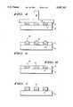
- FIG. 1illustrates an enlarged, cross-sectional view of a first embodiment of the present invention in a beginning stage of fabrication
- FIG. 2illustrates an enlarged, cross-sectional view of the first embodiment of the present invention in an immediate stage of fabrication
- FIG. 3illustrates the first embodiment of the present invention in a later stage of fabrication
- FIG. 4illustrates an enlarged, cross-sectional view of a second embodiment of the present invention in a later stage of fabrication
- FIG. 5illustrates an enlarged, cross-sectional view of a third embodiment of the present invention in a later stage of fabrication
- FIG. 6illustrates the present invention in a later stage of fabrication
- FIG. 7illustrates an enlarged, cross-sectional view of an embodiment of the present invention in a final stage of fabrication
- FIG. 8illustrates a cross-sectional view of an alternative embodiment of the present invention in an intermediate stage of fabrication
- FIG. 9illustrates an enlarged, cross-sectional view of a flip chip assembly utilizing an embodiment of the present invention.
- the present inventionapplies to the formation of electrical contacts on semiconductor chips.
- the present inventioncan also be utilized for the formation of a raised electrical contact on circuit substrates, such as a semiconductor wafer, a printed wire board, a flex circuit, or a metallized ceramic or glass.
- circuit substratessuch as a semiconductor wafer, a printed wire board, a flex circuit, or a metallized ceramic or glass.
- the present inventionis most advantageous for use on semiconductor wafers or chips because this is where it is highly desirable to form electrical contacts having a width or diameter of 50 microns or less.
- FIG. 1illustrates a semiconductor wafer 10 having, for example, a plurality of semiconductor chips (comprised of semiconductor devices such as transistors, diodes or integrated circuits) formed therein (not shown) and having a conductive layer 12 formed on the surface of the semiconductor wafer to make electrical contact to the appropriate regions of the integrated circuit or semiconductor device.
- Conductive layer 12 to be electrically contactedis typically called a bond pad.
- Semiconductor wafer 10is shown in highly simplified form for illustrative convenience.
- wet photoresist 15is applied to the surface of semiconductor wafer 10.
- Wet photoresist 15is contrasted with a dry photoresist laminate.
- Wet photoresist layer 15is not a laminate but is applied by spinning on photoresist layer 15 to the surface of semiconductor wafer 10 in liquid fashion. The liquid or wet photoresist is then hardened or baked to form a solid after it has been applied to the surface of semiconductor wafer 10.
- wet photoresist layer 15is now polymerized, it will still be referred to as a "wet" resist in order to avoid confusion with dry photoresist laminates.
- Wet photoresist layer 15may be a negative or positive resist having characteristics which allow the formation of openings or vias 20 therein. Openings or vias 20 are formed by standard patterning processes used in photolithography.
- Wet photoresist layer 15can be comprised of the many wet chemistry photoresists available on the market, such as a novolak resin or a photo-imagable polyimide.
- the thickness of wet photoresist layer 15is desirably in the range of 20 to 75 microns. The thickness of wet photoresist layer 15 is ultimately determined by the desired height and diameter of the interconnect bump to be formed.
- the thickness of wet photoresist layer 15may be easily changed to any desired thickness by methods such as changing the speed at which semiconductor wafer 10 is spun while wet photoresist layer 15 is applied to the surface or by changing the viscosity of wet photoresist layer 15, or by multiple applications of layers of wet photoresist layer 15. This thickness is in contrast to the thickness of dry resist laminate, which is commercially only available in 10 micron increments, beginning at 20 microns.
- Openings 20overlie at least a portion of conductor layer 12.
- the diameter of opening 20is dependent on the size of conductive layer 12.
- the present inventionis particularly useful where opening 20 has a diameter of less than 50 microns, because, as noted previously, the dry photoresist or metal stencil or screen printing methods used in the past are unable to get down to these geometries.
- openings 20may be self-aligned to conductor layer 12 which forms the bond pad.
- the interconnect bumpis formed by aligning the metal mask to the bond pad by relying on a vision system and mechanical motion of the screen printer parts.
- the metal maskis not in intimate physical contact with the surface of the semiconductor wafer. Thus, large misalignment tolerances must be taken into account that are not present when using a wet photoresist as a mask.
- FIG. 2illustrates the semiconductor structure of FIG. 1 further along in processing.
- a conductive paste 30is applied to the surface of semiconductor wafer 10.
- Conductive paste 30is a polymer that may be comprised of a solder paste or an epoxy paste filled with conductive particles or flakes such as silver, gold, or copper.
- An example of a conductive pasteis Epotek H20E-PFC, available from Epoxy Technology, Inc.
- conductive paste 30is dispensed, spread, or flooded on the surface of semiconductor wafer 10 in order to roughly cover the surface of semiconductor wafer 10.
- FIG. 3illustrates one way to further process the structure of FIG. 2.
- a squeegee 40 or other suitable instrumentis used to sweep conductive paste 30 across wet photoresist layer 15 thereby forcing conductive paste 30 into openings 20 and removing the excess conductive paste 30 off of photoresist mask 15. It is necessary to substantially fill openings 20 and to substantially remove excess conductive paste 30 from the surface of wet photoresist layer 15. Openings 20 are substantially filled in order to provide interconnect bumps of a uniform volume and height. Substantially all of conductive paste 30 is removed means that no significant amount of conductive polymer 30 remains on wet photoresist layer 15 which is touching conductive polymer 30 in openings 20.
- FIG. 4illustrates a second process for forming interconnect bumps after the processing of FIG. 2.
- Pressureis applied to conductive paste 30 through any means, such as a disk 50 having a flat surface.
- disk 50forces conductive paste 30 into openings 20 with excess conductive paste 30 being expelled or squeezed off of the surface of photoresist layer 15.
- FIG. 5illustrates an alternate method of dispensing conductive paste 30 in openings 20.
- dots of conductive paste 30are dispensed into openings 20 with the use of suitable dispensing means.
- suitable meansincludes a dispensing system manufactured by Camalot, Inc. The tail of the dots can be removed and openings 20 completely filled by wiping off the excess or using squeegee 40 illustrated in FIG. 3 or even the process illustrated in FIG. 4.
- FIG. 6illustrates the structure of the present embodiment which results after any of the processing shown in FIG. 3, FIG. 4, or FIG. 5.
- conductive paste 30fills opening 20 so that the surface of conductive paste 30 is planer with wet photoresist layer 15 in order to provide interconnect bumps having substantially the same height.
- conductive paste 30is heated at a temperature above room temperature (cured) so that conductive paste 30 is resistant to a solvent used to remove wet photoresist layer 15 thereafter and will adhere to the surface of conductive layer 12. Before at least partial curing, presently available conductive pastes 30 will not adhere to conductive layer 12 adequately. Curing may preferably take place in an oven having a temperature of 120°-140° C. for approximately 5-10 minutes.
- conductive paste 30is comprised of a solder paste
- curingwould take place at a temperature slightly higher than the solder's eutectic temperature, which is typically between 100°and 350° C.
- a high temperature wet photoresist layer or a photo-imagable polyimidewould be required for use with a solder paste that cures at a temperature above 150° C. In any event, curing for a time less than a time where a wet photoresist residue is formed on the substrate that can not be later removed is necessary.
- FIG. 7illustrates the structure of FIG. 6 further along in processing.
- Wet photoresist layer 15is removed by suitable methods well known in the art.
- a solventsuch as acetone or other photoresist stripper is used to remove wet photoresist layer 15.
- an oxygen (O 2 ) plasma ashermay be used.
- a small amount of conductive paste 30may be left remaining on wet photoresist layer 15 as long as it is a small enough amount that can be removed with wet photoresist layer 15.
- wet photoresist layer 15is comprised of a photo-imagable polyimide, then it does not need to be removed because it can act as a passivation layer.
- conductive paste 30may be further cured after wet photoresist layer 15 is removed in order to further harden conductive paste 30 now in the form of interconnect bumps for better mechanical integrity and moisture resistance. It is important to note that this second curing is desirably performed after wet photoresist layer 15 is removed because too much exposure of wet photoresist layer 15 to these temperatures for substantially greater than 10 minutes can result in the formation of a residue of wet photoresist layer 15 that can not be removed from the surface of semiconductor wafer 10.
- the second curingis preferably performed at temperatures between 150°-300° C. for at least 5-60 minutes. Ultimately, the time and temperature of both cure cycles will be determined by the characteristics of specific conductive pastes used. Some types of conductive pastes may not require the second curing process.
- FIG. 8illustrates an alternative embodiment of the present invention in an intermediate stage of fabrication. Elements that are the same as shown in FIG. 1 are referenced by the same numerals.
- This figureillustrates semiconductor wafer 10 in more detail. Processing of this embodiment is the same as the embodiment illustrated in FIG. 1, however, here a passivation layer 13 is shown formed on the surface of semiconductor wafer 10 and conductive layer 12. A wet photoresist layer 15 is formed and patterned on the surface of passivation layer 13 to provide openings 20. Here, a portion of passivation layer is removed overlying a portion of conductive layer 12. Subsequently, a conductive paste may then be applied in any of the manners described above with reference to FIGS. 2-7.
- the advantage of this processis that the same photoresist that is used to pattern passivation layer 13 can be utilized to form the interconnect bumps.
- interconnect bumpswill be self-aligned to conductive layer 12 and an additional masking process of spinning on an additional wet photoresist layer 15 and removing it will be saved. This will reduce costs and improve cycle time.
- the removal of wet photoresist layer 15is the same as described above. Note that the benefits of this process can not be obtained with the use of a dry resist laminate because the wet photoresist layer used to pattern passivation layer 13 can not be additionally utilized for forming conductive paste 30.
- wet photoresist layer 15 used to pattern passivation layer 13can not be replaced with a dry photoresist laminate, because dry resist laminates can not print small geometries and do not have the necessary definition for small pitches that are achievable with wet chemistry photoresists.
- FIG. 9illustrates a method for forming a flip chip assembly using the techniques of the present invention.
- a wet photoresist layer 15is provided on a substrate 60 and patterned to form openings.
- Substrate 60may be comprised of another semiconductor wafer, a printed circuit board, a flex circuit, or a metallized ceramic glass.
- a conductive paste 30is formed in the openings of wet photoresist layer 15 as described above resulting in either embodiment shown in FIG. 7 or 8.
- a singulated chip 70 having a plurality of electrical interconnects formed thereonis preferably prepared from semiconductor wafer 10 as above in FIG.
- Singulated chip 70is singulated, by methods well known in the art, from semiconductor wafer 10, as shown in FIG. 1, which is comprised of a plurality of chips 70.
- a partial curealso referred to as a B-stage cure, is performed as described above and wet photoresist layer 15 is removed in accordance with the teachings above, and if necessary, a second cure is performed.
- the mating of substrate 60 and chip 70must be performed before the final or second curing of conductive paste 30 of either substrate 60 or chip 70.
- conductive paste 30 on both substrate 60 and chip 70are fully cured before mating, then conductive paste 30 of substrate 60 and chip 70 will not adhere to each other thereafter.
- a wet photoresist layercan be used in conjunction with conductive pastes to form an electrical interconnect, typically called an interconnect bump, on a semiconductor wafer in order to provide interconnect bumps having diameters or widths less than 50 microns.
- the ability to print small geometries with submicron accuracy in the masking layeris essential to the formation of interconnect bumps having small geometries. This capability and accuracy was not available with the use of dry photoresist laminates or stencil/screen printing with a metal mask as used in the past.
- the present inventionallows bump geometry reduction and bump registration accuracy over the use of dry photoresist or metal mask screen/stencil printing technology.
- the interconnect bumps formed by the present inventionare particularly advantageous for use with flip chip assembly requiring ultra-fine geometries and pitches.
Landscapes
- Engineering & Computer Science (AREA)
- Computer Hardware Design (AREA)
- Microelectronics & Electronic Packaging (AREA)
- Power Engineering (AREA)
- Manufacturing & Machinery (AREA)
- Wire Bonding (AREA)
Abstract
Description
Claims (16)
Priority Applications (1)
| Application Number | Priority Date | Filing Date | Title |
|---|---|---|---|
| US08/415,972US5587342A (en) | 1995-04-03 | 1995-04-03 | Method of forming an electrical interconnect |
Applications Claiming Priority (1)
| Application Number | Priority Date | Filing Date | Title |
|---|---|---|---|
| US08/415,972US5587342A (en) | 1995-04-03 | 1995-04-03 | Method of forming an electrical interconnect |
Publications (1)
| Publication Number | Publication Date |
|---|---|
| US5587342Atrue US5587342A (en) | 1996-12-24 |
Family
ID=23647995
Family Applications (1)
| Application Number | Title | Priority Date | Filing Date |
|---|---|---|---|
| US08/415,972Expired - LifetimeUS5587342A (en) | 1995-04-03 | 1995-04-03 | Method of forming an electrical interconnect |
Country Status (1)
| Country | Link |
|---|---|
| US (1) | US5587342A (en) |
Cited By (52)
| Publication number | Priority date | Publication date | Assignee | Title |
|---|---|---|---|---|
| FR2762715A1 (en)* | 1997-04-28 | 1998-10-30 | Novatec | METHOD FOR MAKING AND BRAZING ELECTRICAL CONNECTION BALLS ON RECEPTION RANGES OF ELECTRICAL CONNECTION OF CIRCUITS OR ELECTRONIC COMPONENTS AND DEVICE FOR IMPLEMENTING THE SAME |
| FR2762714A1 (en)* | 1997-04-28 | 1998-10-30 | Novatec | Connection metal beads for connecting electronic components |
| US5830803A (en)* | 1994-01-11 | 1998-11-03 | Siemens Aktiengesellschaft | Method for filling contact holes using a doctor blade |
| US6085968A (en)* | 1999-01-22 | 2000-07-11 | Hewlett-Packard Company | Solder retention ring for improved solder bump formation |
| US6207550B1 (en)* | 1997-07-02 | 2001-03-27 | Matsushita Electric Industrial Co., Ltd. | Method for fabricating bump electrodes with a leveling step for uniform heights |
| US20010002044A1 (en)* | 1999-08-27 | 2001-05-31 | Ball Michael B. | Method of disposing conductive bumps onto a semiconductor device and semiconductor devices so formed |
| EP1162654A1 (en)* | 2000-06-06 | 2001-12-12 | I-Ming Chen | Method for mounting a semiconductor chip on a substrate, and semiconductor device adapted for mounting on a substrate |
| US6335571B1 (en) | 1997-07-21 | 2002-01-01 | Miguel Albert Capote | Semiconductor flip-chip package and method for the fabrication thereof |
| US20020014703A1 (en)* | 1997-07-21 | 2002-02-07 | Capote Miguel A. | Semiconductor flip-chip package and method for the fabrication thereof |
| US6399426B1 (en) | 1998-07-21 | 2002-06-04 | Miguel Albert Capote | Semiconductor flip-chip package and method for the fabrication thereof |
| US6426281B1 (en) | 2001-01-16 | 2002-07-30 | Taiwan Semiconductor Manufacturing Company | Method to form bump in bumping technology |
| US6451127B1 (en) | 1999-06-01 | 2002-09-17 | Motorola, Inc. | Conductive paste and semiconductor component having conductive bumps made from the conductive paste |
| DE10137346A1 (en)* | 2001-07-31 | 2003-02-27 | Infineon Technologies Ag | Chip device with at least one microchip, has solder applied to trench formed in trench layer on insulating layer, to create conductive track |
| US6555296B2 (en)* | 2001-04-04 | 2003-04-29 | Siliconware Precision Industries Co., Ltd. | Fine pitch wafer bumping process |
| US6636313B2 (en)* | 2002-01-12 | 2003-10-21 | Taiwan Semiconductor Manufacturing Co. Ltd | Method of measuring photoresist and bump misalignment |
| US6656750B1 (en)* | 1999-04-29 | 2003-12-02 | International Business Machines Corporation | Method for testing chips on flat solder bumps |
| US6656829B2 (en)* | 2000-03-14 | 2003-12-02 | Hitachi, Ltd. | Semiconductor integrated circuit device and manufacturing method of that |
| US6660944B1 (en)* | 1996-03-29 | 2003-12-09 | Ngk Spark Plug Co., Ltd. | Circuit board having solder bumps |
| US6805541B1 (en)* | 1999-02-15 | 2004-10-19 | Kabushiki Kaisha Toshiba | Resin encapsulating apparatus used in a manufacture of a semiconductor device |
| US20040232562A1 (en)* | 2003-05-23 | 2004-11-25 | Texas Instruments Incorporated | System and method for increasing bump pad height |
| US20050014311A1 (en)* | 1996-12-02 | 2005-01-20 | Kabushiki Kaisha Toshiba | Multichip semiconductor device, chip therefor and method of formation thereof |
| US20050032272A1 (en)* | 2003-08-08 | 2005-02-10 | University Of Delaware | Method for creating flip-chip conductive-polymer bumps using photolithography and polishing |
| US20060088998A1 (en)* | 2004-10-27 | 2006-04-27 | Seiko Epson Corporation | Wiring pattern forming method, film pattern forming method, semiconductor device, electro-optical device, and electronic equipment |
| US20060270079A1 (en)* | 2005-05-24 | 2006-11-30 | Ling Liu | Method and circuit structure employing a photo-imaged solder mask |
| US20070099325A1 (en)* | 2005-10-27 | 2007-05-03 | Lg Innotek Co., Ltd | Light emitting diode device, manufacturing method of the light emitting diode device and mounting structure of the light emitting diode device |
| US7250330B2 (en)* | 2002-10-29 | 2007-07-31 | International Business Machines Corporation | Method of making an electronic package |
| US7253078B1 (en) | 1999-07-22 | 2007-08-07 | National Semiconductor Corporation | Method and apparatus for forming an underfill adhesive layer |
| US7282375B1 (en) | 2004-04-14 | 2007-10-16 | National Semiconductor Corporation | Wafer level package design that facilitates trimming and testing |
| US7301222B1 (en) | 2003-02-12 | 2007-11-27 | National Semiconductor Corporation | Apparatus for forming a pre-applied underfill adhesive layer for semiconductor wafer level chip-scale packages |
| US20080138934A1 (en)* | 2004-02-06 | 2008-06-12 | Samsung Electronics Co., Ltd. | Method of manufacturing multi-stack package |
| US7423337B1 (en) | 2002-08-19 | 2008-09-09 | National Semiconductor Corporation | Integrated circuit device package having a support coating for improved reliability during temperature cycling |
| US20080241992A1 (en)* | 2001-03-05 | 2008-10-02 | Megica Corporation | Method of assembling chips |
| US20090146303A1 (en)* | 2007-09-28 | 2009-06-11 | Tessera, Inc. | Flip Chip Interconnection with double post |
| US20090188706A1 (en)* | 2007-12-25 | 2009-07-30 | Tessera Interconnect Materials, Inc. | Interconnection element for electric circuits |
| US20100193970A1 (en)* | 2003-12-30 | 2010-08-05 | Tessera, Inc. | Micro pin grid array with pin motion isolation |
| US7855461B2 (en) | 2003-12-08 | 2010-12-21 | Megica Corporation | Chip structure with bumps and testing pads |
| US20110316201A1 (en)* | 2010-06-24 | 2011-12-29 | Taiwan Semiconductor Manufacturing Company, Ltd. | Wafer Level Packaging Using Blade Molding |
| US8330272B2 (en) | 2010-07-08 | 2012-12-11 | Tessera, Inc. | Microelectronic packages with dual or multiple-etched flip-chip connectors |
| US8580607B2 (en) | 2010-07-27 | 2013-11-12 | Tessera, Inc. | Microelectronic packages with nanoparticle joining |
| US8604348B2 (en) | 2003-10-06 | 2013-12-10 | Tessera, Inc. | Method of making a connection component with posts and pads |
| US8641913B2 (en) | 2003-10-06 | 2014-02-04 | Tessera, Inc. | Fine pitch microcontacts and method for forming thereof |
| WO2014104846A1 (en)* | 2012-12-28 | 2014-07-03 | 주식회사 잉크테크 | Method for forming conductive pattern, conductive film, conductive pattern, and transparent conductive film |
| US8853558B2 (en) | 2010-12-10 | 2014-10-07 | Tessera, Inc. | Interconnect structure |
| US9543490B2 (en) | 2010-09-24 | 2017-01-10 | Seoul Semiconductor Co., Ltd. | Wafer-level light emitting diode package and method of fabricating the same |
| US9633971B2 (en) | 2015-07-10 | 2017-04-25 | Invensas Corporation | Structures and methods for low temperature bonding using nanoparticles |
| CN107994002A (en)* | 2014-12-30 | 2018-05-04 | 日月光半导体制造股份有限公司 | Semiconductor substrate and semiconductor packaging structure with same |
| US10535626B2 (en) | 2015-07-10 | 2020-01-14 | Invensas Corporation | Structures and methods for low temperature bonding using nanoparticles |
| US10580929B2 (en) | 2016-03-30 | 2020-03-03 | Seoul Viosys Co., Ltd. | UV light emitting diode package and light emitting diode module having the same |
| US10658300B2 (en) | 2018-01-17 | 2020-05-19 | Samsung Electronics Co., Ltd. | Semiconductor package and semiconductor device including the same |
| EP3852139A3 (en)* | 2019-12-27 | 2021-09-08 | STMicroelectronics Pte Ltd. | Wafer level chip scale package with co-planar bumps with different solder heights and corresponding manufacturing method |
| US11973056B2 (en) | 2016-10-27 | 2024-04-30 | Adeia Semiconductor Technologies Llc | Methods for low temperature bonding using nanoparticles |
| US12211809B2 (en) | 2020-12-30 | 2025-01-28 | Adeia Semiconductor Bonding Technologies Inc. | Structure with conductive feature and method of forming same |
Citations (12)
| Publication number | Priority date | Publication date | Assignee | Title |
|---|---|---|---|---|
| US4806706A (en)* | 1987-04-08 | 1989-02-21 | Nippon Cmk Corp. | Printed wiring board |
| US5093279A (en)* | 1991-02-01 | 1992-03-03 | International Business Machines Corporation | Laser ablation damascene process |
| US5100501A (en)* | 1989-06-30 | 1992-03-31 | Texas Instruments Incorporated | Process for selectively depositing a metal in vias and contacts by using a sacrificial layer |
| US5149671A (en)* | 1990-12-03 | 1992-09-22 | Grumman Aerospace Corporation | Method for forming multilayer indium bump contact |
| US5169800A (en)* | 1989-12-26 | 1992-12-08 | Fujitsu Limited | Method of fabricating semiconductor devices by laser planarization of metal layer |
| US5246880A (en)* | 1992-04-27 | 1993-09-21 | Eastman Kodak Company | Method for creating substrate electrodes for flip chip and other applications |
| US5266446A (en)* | 1990-11-15 | 1993-11-30 | International Business Machines Corporation | Method of making a multilayer thin film structure |
| US5280414A (en)* | 1990-06-11 | 1994-01-18 | International Business Machines Corp. | Au-Sn transient liquid bonding in high performance laminates |
| US5376229A (en)* | 1993-10-05 | 1994-12-27 | Miller; Jeffrey N. | Method of fabrication of adjacent coplanar semiconductor devices |
| US5409862A (en)* | 1992-03-24 | 1995-04-25 | Kabushiki Kaisha Toshiba | Method for making aluminum single crystal interconnections on insulators |
| US5411918A (en)* | 1990-07-18 | 1995-05-02 | Raychem Limited | Processing microchips |
| US5446247A (en)* | 1993-11-19 | 1995-08-29 | Motorola, Inc. | Electrical contact and method for making an electrical contact |
- 1995
- 1995-04-03USUS08/415,972patent/US5587342A/ennot_activeExpired - Lifetime
Patent Citations (12)
| Publication number | Priority date | Publication date | Assignee | Title |
|---|---|---|---|---|
| US4806706A (en)* | 1987-04-08 | 1989-02-21 | Nippon Cmk Corp. | Printed wiring board |
| US5100501A (en)* | 1989-06-30 | 1992-03-31 | Texas Instruments Incorporated | Process for selectively depositing a metal in vias and contacts by using a sacrificial layer |
| US5169800A (en)* | 1989-12-26 | 1992-12-08 | Fujitsu Limited | Method of fabricating semiconductor devices by laser planarization of metal layer |
| US5280414A (en)* | 1990-06-11 | 1994-01-18 | International Business Machines Corp. | Au-Sn transient liquid bonding in high performance laminates |
| US5411918A (en)* | 1990-07-18 | 1995-05-02 | Raychem Limited | Processing microchips |
| US5266446A (en)* | 1990-11-15 | 1993-11-30 | International Business Machines Corporation | Method of making a multilayer thin film structure |
| US5149671A (en)* | 1990-12-03 | 1992-09-22 | Grumman Aerospace Corporation | Method for forming multilayer indium bump contact |
| US5093279A (en)* | 1991-02-01 | 1992-03-03 | International Business Machines Corporation | Laser ablation damascene process |
| US5409862A (en)* | 1992-03-24 | 1995-04-25 | Kabushiki Kaisha Toshiba | Method for making aluminum single crystal interconnections on insulators |
| US5246880A (en)* | 1992-04-27 | 1993-09-21 | Eastman Kodak Company | Method for creating substrate electrodes for flip chip and other applications |
| US5376229A (en)* | 1993-10-05 | 1994-12-27 | Miller; Jeffrey N. | Method of fabrication of adjacent coplanar semiconductor devices |
| US5446247A (en)* | 1993-11-19 | 1995-08-29 | Motorola, Inc. | Electrical contact and method for making an electrical contact |
Cited By (91)
| Publication number | Priority date | Publication date | Assignee | Title |
|---|---|---|---|---|
| US5830803A (en)* | 1994-01-11 | 1998-11-03 | Siemens Aktiengesellschaft | Method for filling contact holes using a doctor blade |
| US6660944B1 (en)* | 1996-03-29 | 2003-12-09 | Ngk Spark Plug Co., Ltd. | Circuit board having solder bumps |
| US20050014311A1 (en)* | 1996-12-02 | 2005-01-20 | Kabushiki Kaisha Toshiba | Multichip semiconductor device, chip therefor and method of formation thereof |
| US8174093B2 (en) | 1996-12-02 | 2012-05-08 | Kabushiki Kaisha Toshiba | Multichip semiconductor device, chip therefor and method of formation thereof |
| US8283755B2 (en) | 1996-12-02 | 2012-10-09 | Kabushiki Kaisha Toshiba | Multichip semiconductor device, chip therefor and method of formation thereof |
| US7335517B2 (en)* | 1996-12-02 | 2008-02-26 | Kabushiki Kaisha Toshiba | Multichip semiconductor device, chip therefor and method of formation thereof |
| US20110215443A1 (en)* | 1996-12-02 | 2011-09-08 | Kabushiki Kaisha Toshiba | Multichip semiconductor device, chip therefor and method of formation thereof |
| US7829975B2 (en)* | 1996-12-02 | 2010-11-09 | Kabushiki Kaisha Toshiba | Multichip semiconductor device, chip therefor and method of formation thereof |
| WO1998049725A1 (en)* | 1997-04-28 | 1998-11-05 | Societe Novatec S.A. | Method for making connection balls on electronic circuits or components |
| FR2762715A1 (en)* | 1997-04-28 | 1998-10-30 | Novatec | METHOD FOR MAKING AND BRAZING ELECTRICAL CONNECTION BALLS ON RECEPTION RANGES OF ELECTRICAL CONNECTION OF CIRCUITS OR ELECTRONIC COMPONENTS AND DEVICE FOR IMPLEMENTING THE SAME |
| US6689412B1 (en)* | 1997-04-28 | 2004-02-10 | Societe Novatec S.A. | Method for making connection balls on electronic circuits or components |
| FR2762714A1 (en)* | 1997-04-28 | 1998-10-30 | Novatec | Connection metal beads for connecting electronic components |
| US6207550B1 (en)* | 1997-07-02 | 2001-03-27 | Matsushita Electric Industrial Co., Ltd. | Method for fabricating bump electrodes with a leveling step for uniform heights |
| US6335571B1 (en) | 1997-07-21 | 2002-01-01 | Miguel Albert Capote | Semiconductor flip-chip package and method for the fabrication thereof |
| US20020014703A1 (en)* | 1997-07-21 | 2002-02-07 | Capote Miguel A. | Semiconductor flip-chip package and method for the fabrication thereof |
| US6399426B1 (en) | 1998-07-21 | 2002-06-04 | Miguel Albert Capote | Semiconductor flip-chip package and method for the fabrication thereof |
| US6085968A (en)* | 1999-01-22 | 2000-07-11 | Hewlett-Packard Company | Solder retention ring for improved solder bump formation |
| US6805541B1 (en)* | 1999-02-15 | 2004-10-19 | Kabushiki Kaisha Toshiba | Resin encapsulating apparatus used in a manufacture of a semiconductor device |
| US6656750B1 (en)* | 1999-04-29 | 2003-12-02 | International Business Machines Corporation | Method for testing chips on flat solder bumps |
| US20040087046A1 (en)* | 1999-04-29 | 2004-05-06 | International Business Machines Corporation. | Method for testing chips on flat solder bumps |
| US6451127B1 (en) | 1999-06-01 | 2002-09-17 | Motorola, Inc. | Conductive paste and semiconductor component having conductive bumps made from the conductive paste |
| US6669079B2 (en) | 1999-06-01 | 2003-12-30 | Motorola, Inc. | Conductive paste and semiconductor component having conductive bumps made from the conductive paste |
| US7253078B1 (en) | 1999-07-22 | 2007-08-07 | National Semiconductor Corporation | Method and apparatus for forming an underfill adhesive layer |
| US6861345B2 (en)* | 1999-08-27 | 2005-03-01 | Micron Technology, Inc. | Method of disposing conductive bumps onto a semiconductor device |
| US20050142835A1 (en)* | 1999-08-27 | 2005-06-30 | Ball Michael B. | Method of disposing conductive bumps onto a semiconductor device and semiconductor devices so formed |
| US20010002044A1 (en)* | 1999-08-27 | 2001-05-31 | Ball Michael B. | Method of disposing conductive bumps onto a semiconductor device and semiconductor devices so formed |
| US6656829B2 (en)* | 2000-03-14 | 2003-12-02 | Hitachi, Ltd. | Semiconductor integrated circuit device and manufacturing method of that |
| EP1162654A1 (en)* | 2000-06-06 | 2001-12-12 | I-Ming Chen | Method for mounting a semiconductor chip on a substrate, and semiconductor device adapted for mounting on a substrate |
| US6426281B1 (en) | 2001-01-16 | 2002-07-30 | Taiwan Semiconductor Manufacturing Company | Method to form bump in bumping technology |
| US6936923B2 (en) | 2001-01-16 | 2005-08-30 | Taiwan Semiconductor Manufacturing Co., Ltd. | Method to form very a fine pitch solder bump using methods of electroplating |
| US20080241992A1 (en)* | 2001-03-05 | 2008-10-02 | Megica Corporation | Method of assembling chips |
| US6555296B2 (en)* | 2001-04-04 | 2003-04-29 | Siliconware Precision Industries Co., Ltd. | Fine pitch wafer bumping process |
| DE10137346A1 (en)* | 2001-07-31 | 2003-02-27 | Infineon Technologies Ag | Chip device with at least one microchip, has solder applied to trench formed in trench layer on insulating layer, to create conductive track |
| US6636313B2 (en)* | 2002-01-12 | 2003-10-21 | Taiwan Semiconductor Manufacturing Co. Ltd | Method of measuring photoresist and bump misalignment |
| US7423337B1 (en) | 2002-08-19 | 2008-09-09 | National Semiconductor Corporation | Integrated circuit device package having a support coating for improved reliability during temperature cycling |
| US8421222B2 (en) | 2002-10-25 | 2013-04-16 | Megica Corporation | Chip package having a chip combined with a substrate via a copper pillar |
| US7250330B2 (en)* | 2002-10-29 | 2007-07-31 | International Business Machines Corporation | Method of making an electronic package |
| US7413927B1 (en) | 2003-02-12 | 2008-08-19 | National Semiconductor Corporation | Apparatus for forming a pre-applied underfill adhesive layer for semiconductor wafer level chip-scale packages |
| US7301222B1 (en) | 2003-02-12 | 2007-11-27 | National Semiconductor Corporation | Apparatus for forming a pre-applied underfill adhesive layer for semiconductor wafer level chip-scale packages |
| US20040232562A1 (en)* | 2003-05-23 | 2004-11-25 | Texas Instruments Incorporated | System and method for increasing bump pad height |
| US20050032272A1 (en)* | 2003-08-08 | 2005-02-10 | University Of Delaware | Method for creating flip-chip conductive-polymer bumps using photolithography and polishing |
| US7109107B2 (en)* | 2003-08-08 | 2006-09-19 | University Of Delaware | Method for creating flip-chip conductive-polymer bumps using photolithography and polishing |
| WO2005084163A3 (en)* | 2003-08-08 | 2008-10-16 | Univ Delaware | Method for creating flip-chip conductive polymer bumps using photolithography and polishing |
| US8604348B2 (en) | 2003-10-06 | 2013-12-10 | Tessera, Inc. | Method of making a connection component with posts and pads |
| US8641913B2 (en) | 2003-10-06 | 2014-02-04 | Tessera, Inc. | Fine pitch microcontacts and method for forming thereof |
| US7855461B2 (en) | 2003-12-08 | 2010-12-21 | Megica Corporation | Chip structure with bumps and testing pads |
| US8531039B2 (en) | 2003-12-30 | 2013-09-10 | Tessera, Inc. | Micro pin grid array with pin motion isolation |
| US20100193970A1 (en)* | 2003-12-30 | 2010-08-05 | Tessera, Inc. | Micro pin grid array with pin motion isolation |
| US20080138934A1 (en)* | 2004-02-06 | 2008-06-12 | Samsung Electronics Co., Ltd. | Method of manufacturing multi-stack package |
| US7282375B1 (en) | 2004-04-14 | 2007-10-16 | National Semiconductor Corporation | Wafer level package design that facilitates trimming and testing |
| US20060088998A1 (en)* | 2004-10-27 | 2006-04-27 | Seiko Epson Corporation | Wiring pattern forming method, film pattern forming method, semiconductor device, electro-optical device, and electronic equipment |
| US7622385B2 (en)* | 2004-10-27 | 2009-11-24 | Seiko Epson Corporation | Wiring pattern forming method, film pattern forming method, semiconductor device, electro-optical device, and electronic equipment |
| US7326636B2 (en)* | 2005-05-24 | 2008-02-05 | Agilent Technologies, Inc. | Method and circuit structure employing a photo-imaged solder mask |
| US20060270079A1 (en)* | 2005-05-24 | 2006-11-30 | Ling Liu | Method and circuit structure employing a photo-imaged solder mask |
| US8343784B2 (en)* | 2005-10-27 | 2013-01-01 | Lg Innotek Co., Ltd. | Light emitting diode device, manufacturing method of the light emitting diode device and mounting structure of the light emitting diode device |
| US20070099325A1 (en)* | 2005-10-27 | 2007-05-03 | Lg Innotek Co., Ltd | Light emitting diode device, manufacturing method of the light emitting diode device and mounting structure of the light emitting diode device |
| US20090146303A1 (en)* | 2007-09-28 | 2009-06-11 | Tessera, Inc. | Flip Chip Interconnection with double post |
| US8884448B2 (en) | 2007-09-28 | 2014-11-11 | Tessera, Inc. | Flip chip interconnection with double post |
| US8558379B2 (en)* | 2007-09-28 | 2013-10-15 | Tessera, Inc. | Flip chip interconnection with double post |
| US8299368B2 (en) | 2007-12-25 | 2012-10-30 | Invensas Corporation | Interconnection element for electric circuits |
| US20090188706A1 (en)* | 2007-12-25 | 2009-07-30 | Tessera Interconnect Materials, Inc. | Interconnection element for electric circuits |
| US20110316201A1 (en)* | 2010-06-24 | 2011-12-29 | Taiwan Semiconductor Manufacturing Company, Ltd. | Wafer Level Packaging Using Blade Molding |
| US8330272B2 (en) | 2010-07-08 | 2012-12-11 | Tessera, Inc. | Microelectronic packages with dual or multiple-etched flip-chip connectors |
| US8723318B2 (en) | 2010-07-08 | 2014-05-13 | Tessera, Inc. | Microelectronic packages with dual or multiple-etched flip-chip connectors |
| US9030001B2 (en) | 2010-07-27 | 2015-05-12 | Tessera, Inc. | Microelectronic packages with nanoparticle joining |
| US9397063B2 (en) | 2010-07-27 | 2016-07-19 | Tessera, Inc. | Microelectronic packages with nanoparticle joining |
| US8580607B2 (en) | 2010-07-27 | 2013-11-12 | Tessera, Inc. | Microelectronic packages with nanoparticle joining |
| US9882102B2 (en) | 2010-09-24 | 2018-01-30 | Seoul Semiconductor Co., Ltd. | Wafer-level light emitting diode and wafer-level light emitting diode package |
| US10879437B2 (en) | 2010-09-24 | 2020-12-29 | Seoul Semiconductor Co., Ltd. | Wafer-level light emitting diode package and method of fabricating the same |
| US9543490B2 (en) | 2010-09-24 | 2017-01-10 | Seoul Semiconductor Co., Ltd. | Wafer-level light emitting diode package and method of fabricating the same |
| US10069048B2 (en) | 2010-09-24 | 2018-09-04 | Seoul Viosys Co., Ltd. | Wafer-level light emitting diode package and method of fabricating the same |
| US10892386B2 (en) | 2010-09-24 | 2021-01-12 | Seoul Semiconductor Co., Ltd. | Wafer-level light emitting diode package and method of fabricating the same |
| US9496236B2 (en) | 2010-12-10 | 2016-11-15 | Tessera, Inc. | Interconnect structure |
| US8853558B2 (en) | 2010-12-10 | 2014-10-07 | Tessera, Inc. | Interconnect structure |
| CN104919572A (en)* | 2012-12-28 | 2015-09-16 | 印可得株式会社 | Method for forming conductive pattern, conductive film, conductive pattern, and transparent conductive film |
| WO2014104846A1 (en)* | 2012-12-28 | 2014-07-03 | 주식회사 잉크테크 | Method for forming conductive pattern, conductive film, conductive pattern, and transparent conductive film |
| CN107994002B (en)* | 2014-12-30 | 2021-11-30 | 日月光半导体制造股份有限公司 | Semiconductor substrate and semiconductor packaging structure with same |
| CN107994002A (en)* | 2014-12-30 | 2018-05-04 | 日月光半导体制造股份有限公司 | Semiconductor substrate and semiconductor packaging structure with same |
| US9818713B2 (en) | 2015-07-10 | 2017-11-14 | Invensas Corporation | Structures and methods for low temperature bonding using nanoparticles |
| US10886250B2 (en) | 2015-07-10 | 2021-01-05 | Invensas Corporation | Structures and methods for low temperature bonding using nanoparticles |
| US10892246B2 (en) | 2015-07-10 | 2021-01-12 | Invensas Corporation | Structures and methods for low temperature bonding using nanoparticles |
| US10535626B2 (en) | 2015-07-10 | 2020-01-14 | Invensas Corporation | Structures and methods for low temperature bonding using nanoparticles |
| US9633971B2 (en) | 2015-07-10 | 2017-04-25 | Invensas Corporation | Structures and methods for low temperature bonding using nanoparticles |
| US11710718B2 (en) | 2015-07-10 | 2023-07-25 | Adeia Semiconductor Technologies Llc | Structures and methods for low temperature bonding using nanoparticles |
| US10580929B2 (en) | 2016-03-30 | 2020-03-03 | Seoul Viosys Co., Ltd. | UV light emitting diode package and light emitting diode module having the same |
| US11973056B2 (en) | 2016-10-27 | 2024-04-30 | Adeia Semiconductor Technologies Llc | Methods for low temperature bonding using nanoparticles |
| US12027487B2 (en) | 2016-10-27 | 2024-07-02 | Adeia Semiconductor Technologies Llc | Structures for low temperature bonding using nanoparticles |
| US10658300B2 (en) | 2018-01-17 | 2020-05-19 | Samsung Electronics Co., Ltd. | Semiconductor package and semiconductor device including the same |
| EP3852139A3 (en)* | 2019-12-27 | 2021-09-08 | STMicroelectronics Pte Ltd. | Wafer level chip scale package with co-planar bumps with different solder heights and corresponding manufacturing method |
| US11581280B2 (en) | 2019-12-27 | 2023-02-14 | Stmicroelectronics Pte Ltd | WLCSP package with different solder volumes |
| US12211809B2 (en) | 2020-12-30 | 2025-01-28 | Adeia Semiconductor Bonding Technologies Inc. | Structure with conductive feature and method of forming same |
Similar Documents
| Publication | Publication Date | Title |
|---|---|---|
| US5587342A (en) | Method of forming an electrical interconnect | |
| US7157310B2 (en) | Methods for packaging microfeature devices and microfeature devices formed by such methods | |
| US6459150B1 (en) | Electronic substrate having an aperture position through a substrate, conductive pads, and an insulating layer | |
| US6586322B1 (en) | Method of making a bump on a substrate using multiple photoresist layers | |
| US5492863A (en) | Method for forming conductive bumps on a semiconductor device | |
| US6197613B1 (en) | Wafer level packaging method and devices formed | |
| US7608929B2 (en) | Electrical connector structure of circuit board and method for fabricating the same | |
| KR100597993B1 (en) | Bump for Semiconductor Package, Semiconductor Package and Manufacturing Method Applying the Bump | |
| US6372619B1 (en) | Method for fabricating wafer level chip scale package with discrete package encapsulation | |
| US6204089B1 (en) | Method for forming flip chip package utilizing cone shaped bumps | |
| US6967399B2 (en) | Semiconductor device manufacturing method having a step of applying a copper foil on a substrate as a part of a wiring connecting an electrode pad to a mounting terminal | |
| US7462937B2 (en) | Semiconductor device | |
| US6767818B1 (en) | Method for forming electrically conductive bumps and devices formed | |
| KR101009110B1 (en) | Printed circuit board with buried solder bumps and manufacturing method thereof | |
| CN100527373C (en) | Semiconductor device and manufacturing method for the same | |
| US20070052091A1 (en) | Electronic device and method of manufacturing same | |
| US6320127B1 (en) | Method and structure for reducing the incidence of voiding in an underfill layer of an electronic component package | |
| DE10250634B4 (en) | Semiconductor structure with compliant interconnecting element and method of making the same | |
| US7087510B2 (en) | Method of making bondable leads using positive photoresist and structures made therefrom | |
| WO2002080269A2 (en) | Method and structure for ex-situ polymer stud grid array contact formation | |
| KR20080047280A (en) | Semiconductor device and manufacturing method thereof | |
| JP3568869B2 (en) | Semiconductor integrated circuit device and method of manufacturing the same | |
| JP2869907B2 (en) | Connection structure of semiconductor device | |
| KR101865873B1 (en) | method for manufacturing semiconductor package substrate | |
| JP2001135662A (en) | Semiconductor element and semiconductor device manufacturing method |
Legal Events
| Date | Code | Title | Description |
|---|---|---|---|
| AS | Assignment | Owner name:MOTOROLA, INC., ILLINOIS Free format text:ASSIGNMENT OF ASSIGNORS INTEREST;ASSIGNORS:LIN, JONG-KAI;LYTLE, WILLIAM H.;SUBRAHMANYAN, RAVICHANDRAN;REEL/FRAME:007513/0547;SIGNING DATES FROM 19950518 TO 19950522 | |
| STCF | Information on status: patent grant | Free format text:PATENTED CASE | |
| FPAY | Fee payment | Year of fee payment:4 | |
| AS | Assignment | Owner name:FREESCALE SEMICONDUCTOR, INC., TEXAS Free format text:ASSIGNMENT OF ASSIGNORS INTEREST;ASSIGNOR:MOTOROLA, INC.;REEL/FRAME:015698/0657 Effective date:20040404 Owner name:FREESCALE SEMICONDUCTOR, INC.,TEXAS Free format text:ASSIGNMENT OF ASSIGNORS INTEREST;ASSIGNOR:MOTOROLA, INC.;REEL/FRAME:015698/0657 Effective date:20040404 | |
| FPAY | Fee payment | Year of fee payment:8 | |
| AS | Assignment | Owner name:CITIBANK, N.A. AS COLLATERAL AGENT, NEW YORK Free format text:SECURITY AGREEMENT;ASSIGNORS:FREESCALE SEMICONDUCTOR, INC.;FREESCALE ACQUISITION CORPORATION;FREESCALE ACQUISITION HOLDINGS CORP.;AND OTHERS;REEL/FRAME:018855/0129 Effective date:20061201 Owner name:CITIBANK, N.A. AS COLLATERAL AGENT,NEW YORK Free format text:SECURITY AGREEMENT;ASSIGNORS:FREESCALE SEMICONDUCTOR, INC.;FREESCALE ACQUISITION CORPORATION;FREESCALE ACQUISITION HOLDINGS CORP.;AND OTHERS;REEL/FRAME:018855/0129 Effective date:20061201 | |
| FPAY | Fee payment | Year of fee payment:12 | |
| AS | Assignment | Owner name:CITIBANK, N.A., AS COLLATERAL AGENT,NEW YORK Free format text:SECURITY AGREEMENT;ASSIGNOR:FREESCALE SEMICONDUCTOR, INC.;REEL/FRAME:024397/0001 Effective date:20100413 Owner name:CITIBANK, N.A., AS COLLATERAL AGENT, NEW YORK Free format text:SECURITY AGREEMENT;ASSIGNOR:FREESCALE SEMICONDUCTOR, INC.;REEL/FRAME:024397/0001 Effective date:20100413 | |
| AS | Assignment | Owner name:CITIBANK, N.A., AS NOTES COLLATERAL AGENT, NEW YORK Free format text:SECURITY AGREEMENT;ASSIGNOR:FREESCALE SEMICONDUCTOR, INC.;REEL/FRAME:030633/0424 Effective date:20130521 Owner name:CITIBANK, N.A., AS NOTES COLLATERAL AGENT, NEW YOR Free format text:SECURITY AGREEMENT;ASSIGNOR:FREESCALE SEMICONDUCTOR, INC.;REEL/FRAME:030633/0424 Effective date:20130521 | |
| AS | Assignment | Owner name:CITIBANK, N.A., AS NOTES COLLATERAL AGENT, NEW YORK Free format text:SECURITY AGREEMENT;ASSIGNOR:FREESCALE SEMICONDUCTOR, INC.;REEL/FRAME:031591/0266 Effective date:20131101 Owner name:CITIBANK, N.A., AS NOTES COLLATERAL AGENT, NEW YOR Free format text:SECURITY AGREEMENT;ASSIGNOR:FREESCALE SEMICONDUCTOR, INC.;REEL/FRAME:031591/0266 Effective date:20131101 | |
| AS | Assignment | Owner name:FREESCALE SEMICONDUCTOR, INC., TEXAS Free format text:PATENT RELEASE;ASSIGNOR:CITIBANK, N.A., AS COLLATERAL AGENT;REEL/FRAME:037354/0225 Effective date:20151207 Owner name:FREESCALE SEMICONDUCTOR, INC., TEXAS Free format text:PATENT RELEASE;ASSIGNOR:CITIBANK, N.A., AS COLLATERAL AGENT;REEL/FRAME:037356/0143 Effective date:20151207 Owner name:FREESCALE SEMICONDUCTOR, INC., TEXAS Free format text:PATENT RELEASE;ASSIGNOR:CITIBANK, N.A., AS COLLATERAL AGENT;REEL/FRAME:037356/0553 Effective date:20151207 | |
| AS | Assignment | Owner name:MORGAN STANLEY SENIOR FUNDING, INC., MARYLAND Free format text:ASSIGNMENT AND ASSUMPTION OF SECURITY INTEREST IN PATENTS;ASSIGNOR:CITIBANK, N.A.;REEL/FRAME:037486/0517 Effective date:20151207 | |
| AS | Assignment | Owner name:MORGAN STANLEY SENIOR FUNDING, INC., MARYLAND Free format text:ASSIGNMENT AND ASSUMPTION OF SECURITY INTEREST IN PATENTS;ASSIGNOR:CITIBANK, N.A.;REEL/FRAME:037518/0292 Effective date:20151207 | |
| AS | Assignment | Owner name:NXP, B.V., F/K/A FREESCALE SEMICONDUCTOR, INC., NETHERLANDS Free format text:RELEASE BY SECURED PARTY;ASSIGNOR:MORGAN STANLEY SENIOR FUNDING, INC.;REEL/FRAME:040925/0001 Effective date:20160912 Owner name:NXP, B.V., F/K/A FREESCALE SEMICONDUCTOR, INC., NE Free format text:RELEASE BY SECURED PARTY;ASSIGNOR:MORGAN STANLEY SENIOR FUNDING, INC.;REEL/FRAME:040925/0001 Effective date:20160912 | |
| AS | Assignment | Owner name:NXP B.V., NETHERLANDS Free format text:RELEASE BY SECURED PARTY;ASSIGNOR:MORGAN STANLEY SENIOR FUNDING, INC.;REEL/FRAME:040928/0001 Effective date:20160622 | |
| AS | Assignment | Owner name:MORGAN STANLEY SENIOR FUNDING, INC., MARYLAND Free format text:CORRECTIVE ASSIGNMENT TO CORRECT THE REMOVE PATENTS 8108266 AND 8062324 AND REPLACE THEM WITH 6108266 AND 8060324 PREVIOUSLY RECORDED ON REEL 037518 FRAME 0292. ASSIGNOR(S) HEREBY CONFIRMS THE ASSIGNMENT AND ASSUMPTION OF SECURITY INTEREST IN PATENTS;ASSIGNOR:CITIBANK, N.A.;REEL/FRAME:041703/0536 Effective date:20151207 | |
| AS | Assignment | Owner name:SHENZHEN XINGUODU TECHNOLOGY CO., LTD., CHINA Free format text:CORRECTIVE ASSIGNMENT TO CORRECT THE TO CORRECT THE APPLICATION NO. FROM 13,883,290 TO 13,833,290 PREVIOUSLY RECORDED ON REEL 041703 FRAME 0536. ASSIGNOR(S) HEREBY CONFIRMS THE THE ASSIGNMENT AND ASSUMPTION OF SECURITYINTEREST IN PATENTS.;ASSIGNOR:MORGAN STANLEY SENIOR FUNDING, INC.;REEL/FRAME:048734/0001 Effective date:20190217 | |
| AS | Assignment | Owner name:MORGAN STANLEY SENIOR FUNDING, INC., MARYLAND Free format text:CORRECTIVE ASSIGNMENT TO CORRECT THE REMOVE APPLICATION11759915 AND REPLACE IT WITH APPLICATION 11759935 PREVIOUSLY RECORDED ON REEL 037486 FRAME 0517. ASSIGNOR(S) HEREBY CONFIRMS THE ASSIGNMENT AND ASSUMPTION OF SECURITYINTEREST IN PATENTS;ASSIGNOR:CITIBANK, N.A.;REEL/FRAME:053547/0421 Effective date:20151207 | |
| AS | Assignment | Owner name:NXP B.V., NETHERLANDS Free format text:CORRECTIVE ASSIGNMENT TO CORRECT THE REMOVEAPPLICATION 11759915 AND REPLACE IT WITH APPLICATION11759935 PREVIOUSLY RECORDED ON REEL 040928 FRAME 0001. ASSIGNOR(S) HEREBY CONFIRMS THE RELEASE OF SECURITYINTEREST;ASSIGNOR:MORGAN STANLEY SENIOR FUNDING, INC.;REEL/FRAME:052915/0001 Effective date:20160622 | |
| AS | Assignment | Owner name:NXP, B.V. F/K/A FREESCALE SEMICONDUCTOR, INC., NETHERLANDS Free format text:CORRECTIVE ASSIGNMENT TO CORRECT THE REMOVEAPPLICATION 11759915 AND REPLACE IT WITH APPLICATION11759935 PREVIOUSLY RECORDED ON REEL 040925 FRAME 0001. ASSIGNOR(S) HEREBY CONFIRMS THE RELEASE OF SECURITYINTEREST;ASSIGNOR:MORGAN STANLEY SENIOR FUNDING, INC.;REEL/FRAME:052917/0001 Effective date:20160912 |