US5586585A - Direct loadlock interface - Google Patents
Direct loadlock interfaceDownload PDFInfo
- Publication number
- US5586585A US5586585AUS08/394,698US39469895AUS5586585AUS 5586585 AUS5586585 AUS 5586585AUS 39469895 AUS39469895 AUS 39469895AUS 5586585 AUS5586585 AUS 5586585A
- Authority
- US
- United States
- Prior art keywords
- pod
- chamber
- door
- cassette
- loadlock chamber
- Prior art date
- Legal status (The legal status is an assumption and is not a legal conclusion. Google has not performed a legal analysis and makes no representation as to the accuracy of the status listed.)
- Expired - Lifetime
Links
- 235000012431wafersNutrition0.000claimsabstractdescription211
- 239000004065semiconductorSubstances0.000claimsabstractdescription68
- 238000000034methodMethods0.000claimsabstractdescription62
- 230000008569processEffects0.000claimsabstractdescription49
- 238000012546transferMethods0.000claimsabstractdescription45
- 239000000356contaminantSubstances0.000claimsabstractdescription24
- 230000007246mechanismEffects0.000claimsabstractdescription20
- 238000003860storageMethods0.000claimsabstractdescription12
- 238000004519manufacturing processMethods0.000claimsdescription41
- 238000010926purgeMethods0.000claimsdescription28
- 238000011068loading methodMethods0.000claimsdescription27
- 238000012545processingMethods0.000claimsdescription26
- 239000007789gasSubstances0.000claimsdescription21
- 238000007789sealingMethods0.000claimsdescription11
- 238000002347injectionMethods0.000claimsdescription3
- 239000007924injectionSubstances0.000claimsdescription3
- 238000013519translationMethods0.000claimsdescription3
- 230000001143conditioned effectEffects0.000claimsdescription2
- 239000011261inert gasSubstances0.000claimsdescription2
- 229910052756noble gasInorganic materials0.000claimsdescription2
- 238000000926separation methodMethods0.000claims4
- 230000013011matingEffects0.000claims3
- 230000000284resting effectEffects0.000claims3
- 238000011010flushing procedureMethods0.000claims1
- 239000002245particleSubstances0.000description7
- 238000011109contaminationMethods0.000description6
- 238000000605extractionMethods0.000description6
- 230000008901benefitEffects0.000description5
- IJGRMHOSHXDMSA-UHFFFAOYSA-NAtomic nitrogenChemical compoundN#NIJGRMHOSHXDMSA-UHFFFAOYSA-N0.000description4
- 238000001914filtrationMethods0.000description4
- 239000002184metalSubstances0.000description3
- XLYOFNOQVPJJNP-UHFFFAOYSA-NwaterChemical compoundOXLYOFNOQVPJJNP-UHFFFAOYSA-N0.000description3
- XKRFYHLGVUSROY-UHFFFAOYSA-NArgonChemical compound[Ar]XKRFYHLGVUSROY-UHFFFAOYSA-N0.000description2
- 238000005516engineering processMethods0.000description2
- 229910052757nitrogenInorganic materials0.000description2
- 238000002360preparation methodMethods0.000description2
- 239000012808vapor phaseSubstances0.000description2
- 206010038584Repetitive strain injuryDiseases0.000description1
- 238000013459approachMethods0.000description1
- -1argonChemical compound0.000description1
- 229910052786argonInorganic materials0.000description1
- QVGXLLKOCUKJST-UHFFFAOYSA-Natomic oxygenChemical compound[O]QVGXLLKOCUKJST-UHFFFAOYSA-N0.000description1
- 230000009286beneficial effectEffects0.000description1
- 238000005229chemical vapour depositionMethods0.000description1
- 230000003749cleanlinessEffects0.000description1
- 230000003750conditioning effectEffects0.000description1
- 238000010276constructionMethods0.000description1
- 238000007796conventional methodMethods0.000description1
- 230000006378damageEffects0.000description1
- 238000013461designMethods0.000description1
- 238000009792diffusion processMethods0.000description1
- 238000009826distributionMethods0.000description1
- 238000001704evaporationMethods0.000description1
- 230000008020evaporationEffects0.000description1
- 230000004907fluxEffects0.000description1
- 230000006870functionEffects0.000description1
- 238000001802infusionMethods0.000description1
- 238000002955isolationMethods0.000description1
- 230000007774longtermEffects0.000description1
- 230000005055memory storageEffects0.000description1
- 238000012986modificationMethods0.000description1
- 230000004048modificationEffects0.000description1
- 238000012544monitoring processMethods0.000description1
- 150000002835noble gasesChemical class0.000description1
- 239000001301oxygenSubstances0.000description1
- 229910052760oxygenInorganic materials0.000description1
- 238000001020plasma etchingMethods0.000description1
- 230000001681protective effectEffects0.000description1
- 238000012827research and developmentMethods0.000description1
- 230000000452restraining effectEffects0.000description1
- 239000007787solidSubstances0.000description1
- 238000006467substitution reactionMethods0.000description1
- 239000000758substrateSubstances0.000description1
- 230000003746surface roughnessEffects0.000description1
- 239000012780transparent materialSubstances0.000description1
Images


Classifications
- H—ELECTRICITY
- H01—ELECTRIC ELEMENTS
- H01L—SEMICONDUCTOR DEVICES NOT COVERED BY CLASS H10
- H01L21/00—Processes or apparatus adapted for the manufacture or treatment of semiconductor or solid state devices or of parts thereof
- H01L21/67—Apparatus specially adapted for handling semiconductor or electric solid state devices during manufacture or treatment thereof; Apparatus specially adapted for handling wafers during manufacture or treatment of semiconductor or electric solid state devices or components ; Apparatus not specifically provided for elsewhere
- H01L21/677—Apparatus specially adapted for handling semiconductor or electric solid state devices during manufacture or treatment thereof; Apparatus specially adapted for handling wafers during manufacture or treatment of semiconductor or electric solid state devices or components ; Apparatus not specifically provided for elsewhere for conveying, e.g. between different workstations
- H01L21/67763—Apparatus specially adapted for handling semiconductor or electric solid state devices during manufacture or treatment thereof; Apparatus specially adapted for handling wafers during manufacture or treatment of semiconductor or electric solid state devices or components ; Apparatus not specifically provided for elsewhere for conveying, e.g. between different workstations the wafers being stored in a carrier, involving loading and unloading
- H01L21/67772—Apparatus specially adapted for handling semiconductor or electric solid state devices during manufacture or treatment thereof; Apparatus specially adapted for handling wafers during manufacture or treatment of semiconductor or electric solid state devices or components ; Apparatus not specifically provided for elsewhere for conveying, e.g. between different workstations the wafers being stored in a carrier, involving loading and unloading involving removal of lid, door, cover
- Y—GENERAL TAGGING OF NEW TECHNOLOGICAL DEVELOPMENTS; GENERAL TAGGING OF CROSS-SECTIONAL TECHNOLOGIES SPANNING OVER SEVERAL SECTIONS OF THE IPC; TECHNICAL SUBJECTS COVERED BY FORMER USPC CROSS-REFERENCE ART COLLECTIONS [XRACs] AND DIGESTS
- Y10—TECHNICAL SUBJECTS COVERED BY FORMER USPC
- Y10S—TECHNICAL SUBJECTS COVERED BY FORMER USPC CROSS-REFERENCE ART COLLECTIONS [XRACs] AND DIGESTS
- Y10S414/00—Material or article handling
- Y10S414/135—Associated with semiconductor wafer handling
- Y10S414/139—Associated with semiconductor wafer handling including wafer charging or discharging means for vacuum chamber
- Y—GENERAL TAGGING OF NEW TECHNOLOGICAL DEVELOPMENTS; GENERAL TAGGING OF CROSS-SECTIONAL TECHNOLOGIES SPANNING OVER SEVERAL SECTIONS OF THE IPC; TECHNICAL SUBJECTS COVERED BY FORMER USPC CROSS-REFERENCE ART COLLECTIONS [XRACs] AND DIGESTS
- Y10—TECHNICAL SUBJECTS COVERED BY FORMER USPC
- Y10S—TECHNICAL SUBJECTS COVERED BY FORMER USPC CROSS-REFERENCE ART COLLECTIONS [XRACs] AND DIGESTS
- Y10S414/00—Material or article handling
- Y10S414/135—Associated with semiconductor wafer handling
- Y10S414/14—Wafer cassette transporting
Definitions
- the present inventionrelates to semiconductor wafer manufacturing processes, and in particular, a loadlock chamber for efficient transfer of a wafer cassette from its transfer pod to internal processing stations in a contaminant free environment.
- SMIFstandardized mechanical interface
- the SMIF systemprovides a clean environment for articles by using a small volume of particle-free gas which is controlled with respect to motion, gas flow direction and external contaminants. Further details of one proposed system are described in the paper entitled “SMIF: A TECHNOLOGY FOR WAFER CASSETTE TRANSFER IN VLSI MANUFACTURING,” by Mihir Parikh and Ulrich Kaempf, Solid State Technology, July 1984, pp. 111-115.
- a SMIF systemhas three main components: (1) sealed pods, having a minimal volume, used for storing and transporting cassettes which hold the semiconductor wafers; (2) enclosures placed over cassette ports and wafer processing areas of processing equipment so that the environments inside the pods and enclosures (after having clean air sources) become miniature clean spaces; and (3) a transfer mechanism to load/unload wafer cassettes from a sealed pod without contamination of the wafers in the wafer cassette from external environments.
- the wafer-carrying cassettesare stored and transported between processing stations in the pods. Many of the wafer fabrication processes are carried out in a high vacuum environment. Before entering the ultra high-vacuum processing station, the wafer-carrying cassettes are transferred from the pods to an intermediate vacuum buffer area.
- This buffer areaserves as a buffer for wafer storage and is a gateway for wafer distribution to the vacuum related processes.
- the effectiveness of a loadlock chamberis critical to wafer fabrication and can have a significant impact on the cost of wafer manufacturing and the quality of the finished product.
- Manual loadingcan easily be done if the cassette is of manageable size, but if the cassette is large or heavy, manual loading has certain limitations.
- One limitationis ergonomics. Continued loading and unloading motion by operators is an industry wide concern because of repetitive motion injury. Another limitation is the risk of wafer damage due to human error. A cassette of wafers can be dropped or bumped resulting in the loss of hundreds of thousands of dollars. If manual loading is to be used, provisions must be made for "elbow room" and hand clearance both in the loadlock doorway and within the loadlock chamber. Consequently, conventional loadlock chambers that are manually loaded must be made larger than necessary for just the wafer cassettes alone.
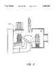
- FIG. 1shows a conventional manual loading system where an operator is transferring a plurality of wafers 6, through an access port 7, and into a conventional loadlock chamber 8. Clearance within the access port and chamber beyond that necessary for the cassette alone must be provided so that the operator may grasp and properly place the cassette within the chamber. Some floor space for the cassette extracting unit is also required for removing the cassette from the SMIF-pod.
- FIG. 2illustrates a conventional swing-arm type device 9 between the cassette extraction unit 11 and the loadlock chamber 8.
- Both manual and automated loading of cassettes into a loadlock chamberadditionally require an extraction device 11 for removing the cassette from the SMIF-pod prior to the chamber loading.
- FIG. 3shows a conventional filtration system that will provide a degree of clean laminar air flow for the cassette and wafer extraction area.
- This type of set-upis expensive to implement and maintain, and it does not completely isolate the wafers from the surrounding particulate contaminants.
- filtration systemsare unable to prevent airborne molecular contaminants, such as water vapor and vapor-phase contaminants, from entering into the loadlock chamber, where they can contaminate the semiconductor wafers.
- Systems for minimizing contaminantsare becoming increasingly more important as wafer manufacturing processes presently require control of particle sizes as small as 0.05 to 0.5 microns.
- the present inventionwhich relates to a loadlock chamber wherein the entire loading sequence has been streamlined to eliminate unnecessary wafer and cassette transfers. Additionally, the transfer of the wafer and cassette to the loadlock chamber according to the present invention occurs in total isolation from the outside environment, thereby preventing contaminants from reaching the wafers, and reducing air-cleanliness requirements for the area near the loadlock chamber and/or the facility in total.
- the cassetteis supported within a pod which is comprised of a pod door on which the cassette rests, and a pod cover which mates with the pod door to provide a sealed environment within the pod.
- the podwhen a cassette is to be transferred to a process chamber, the pod is loaded onto a loadlock chamber such that the pod door lies in contact with a port access door of the loadlock chamber, and the pod cover lies in contact with a port plate assembly of the loadlock chamber, which assembly surrounds the port access door.
- a bottom perimeter of the podregisters against an O-ring gasket on the port plate assembly to form an airtight seal between the pod and the loadlock chamber.
- the port plate assemblyincludes a pair of latches that automatically engage and securely hold the pod cover once the pod is located on the loadlock chamber. Thereafter, a pod door decoupling device within the port access door decouples the pod door from the pod cover. Once the pod door is separated from pod cover, the port plate assembly, having the pod cover supported thereon, moves upward so that the pod cover is separated from the pod door and the cassette, which is supported on the pod door.
- the port plate assemblyfurther includes a pair of pawls positioned on opposite sides of the cassette. During the upward movement of the port plate assembly, the pawls move inward to engage the cassette. As the port plate assembly continues to move upward, the pawls lift the cassette so that the cassette is supported by the port plate assembly and separated from the pod door.
- the port access door and the pod door supported thereonare moved laterally away from the loadlock chamber port access.
- An indexing platform provided within the loadlock chamber below the cassetteis moved upward to engage and support the cassette. Once properly positioned on the indexing platform, the pawls are retracted and the cassette is decoupled from port plate assembly and fully supported by the indexing platform. The indexing platform next lowers the cassette into the loadlock chamber interior. Sensors may be provided on either side of the cassette to provide information with regard to specific wafer location and/or cassette slot location as the cassette is lowered into the chamber interior.
- the port access dooris returned to its position over the loadlock chamber access port to thereby isolate and seal the loadlock chamber.
- the chamber interioris thereafter evacuated to a high-vacuum environment similar to that of the various wafer fabrication processes. Wafers are then extracted from the cassette by a wafer transfer device internal to the fabrication process chambers, and passed by the transfer device into the various process chambers.
- the loadlock chamberis provided with one or more access ports, such as for example modular equipment standardization committee (“MESC”) access ports, to allow transfer of the wafers between the loadlock chamber and the process chambers.
- MSCmodular equipment standardization committee
- a loadlock chamberinclude a plurality of such access ports radially provided around a circumference of the loadlock chamber at differing elevations of the loadlock chamber for allowing wafer access to various vacuum processes. In this way a single loadlock chamber may supply wafers to a plurality of process chambers.
- Another feature of the present inventionis the ability to purge a pod of molecular and/or particulate contaminants by infusing a selected gas into a pod after the pod door has been separated from the pod cover.
- the infusion of gasflushes out or causes the evaporation of contaminants from within the pod. This is beneficial in many applications, especially for long term wafer storage in which the wafers are kept in an inert environment after processing.
- the purging capabilitycan be done during the majority of the loading and unloading sequence, or in parallel when the wafer is in the vacuum chamber being processed.
- the chamberis preferably backfilled with clean air or an inert gas so that the chamber is not exposed to contaminant rich air between cycles.
- FIG. 1is a representation of a manual transfer system for transferring a wafer cassette into a conventional loadlock chamber
- FIG. 2is a representation of an automated transfer system for transferring a wafer cassette into a conventional loadlock chamber
- FIG. 3is a representation of a conventional filtration system used to minimize the presence of contaminants in the cassette transfer area
- FIG. 4is a side view of a loadlock chamber according to the present invention.
- FIG. 4Ais a side cross-sectional view of a loadlock chamber according to the present invention showing the port plate assembly and port access door engaging a transfer pod;
- FIGS. 5 and 5Aare side views of a loadlock chamber according to the present invention showing the cassette and pod cover translating away from the pod door;
- FIG. 6is a side view of a loadlock chamber according to the present invention with the port access door and pod door translating away from the port access;
- FIGS. 7-8are side views of a loadlock chamber according to the present invention with the wafer cassette supported on an indexing platform;
- FIG. 9is a side view of the loadlock chamber according to the present invention with the cassette sealed within the loadlock chamber interior;
- FIG. 10is a perspective view of a loadlock chamber according to the present invention in relation to wafer processing chambers;
- FIG. 11is a side view of a loadlock chamber according to the present invention showing a plurality of access ports
- FIG. 12is a loadlock chamber according to the present invention holding a plurality of stacked cassettes.
- FIG. 13is a side view of a loadlock chamber showing the gas purging feature according to the present invention.
- FIGS. 4 through 13relate in general to an intermediate chamber, such as a loadlock chamber, for allowing transfer of semiconductor wafers from ambient conditions to high-vacuum fabrication chambers.
- the inventionwill be described herein with regard to semiconductor wafers having a 300 mm diameter, which wafers may be stored and transferred within a SMIF-pod. It is understood, however, that the present invention may operate with semiconductor wafers of various sizes and shapes.
- semiconductor waferor "wafer” as used herein refers to a wafer substrate as it may exist in any of the various stages of the semiconductor wafer fabrication process.
- the present inventionis not limited to use with SMIF-pods, and may operate in conjunction with any of various containers used to store and transfer the semiconductor wafers.
- the semiconductor wafersare supported in a support structure such as cassette 12 shown in FIGS. 4 and 4A and described in U.S. application Ser. No. 08/311,954 previously incorporated by reference.
- the cassetteincludes top and bottom plates of substantially circular shape. Attached to and extending between the top and bottom plates are four columns; two side columns, and two rear columns. The side columns are both provided with a plurality of shelves, each shelf defining a plane in which a single semiconductor wafer 16 may be securely supported.
- the plurality of shelvestogether support the plurality of wafers in a parallel and coaxial relation.
- the shelves and columnstogether also define an opening in the cassette through which wafers are inserted and extracted from the cassette.
- the spacing of the wafers within the cassetteis largely dictated by a wafer transfer device, described hereinafter, which slides between adjacent wafers to lift and slide a wafer out of the cassette for processing. It is understood that the present invention may operate with cassettes of various form factors, shapes and designs.
- the cassette 12may be stored and transported in a conventional SMIF-pod 22 that includes a pod cover 14 and pod door 23.
- the cassetteis normally supported on the pod door during storage and transport of the cassette.
- a sealing gasket 37(FIG. 4A) is provided between the cover 14 and door 23 to isolate and seal the interior of pod 22 against the external environment.
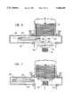
- FIGS. 4 and 4Ashow a loadlock chamber 20 according to the present invention with a pod 22 located thereon.
- the loadlock chamber 20includes a port plate assembly 21 having pod cover restraint latches 24a and 24b, pawls 38a and 38b, and a perimeter O-ring gasket 25.
- Loadlock chamber 20further includes port access door 26, purging chamber 28, interior operation chamber 30, indexing platform 32 mounted on telescopic shaft 45, and at least one access port 36.
- a central processing unit (“CPU”)(not shown) is provided for controlling the operation of, and for monitoring feedback signals from, the various components of the loadlock chamber 20.
- the pod 22In preparation for transferring the wafers 16 into the various wafer fabrication process chambers, the pod 22 is manually or automatedly seated on top of the loadlock chamber.
- the top of the loadlock chambermay include a plurality of angled guide blocks (not shown) to allow easy guidance of the pod into proper position on top of the loadlock chamber.
- the pod door 23When properly located on top of the loadlock chamber 20, the pod door 23 lies in contact with the port access door 26, and the outer rim of pod cover 14 lies in contact with the port plate assembly 21. In this position, a bottom perimeter of the pod cover 14 registers against the O-ring gasket 25 on the port plate assembly to form an airtight seal between the pod 22 and the port plate assembly 21.
- Pod cover restraint latches 24a and 24bare provided to secure the pod cover 14 to the port plate assembly 21. Once the pod 22 is properly positioned on the loadlock chamber, the latches 24a and 24b are pivoted from a first position shown in FIGS. 4 and 4A to a second position shown in FIGS. 5 and 5A. In the second position, the latches 24a and 24b positively secure the pod cover to the port plate assembly.
- the movement of the latches 24a and 24b between the first and second positionsmay be accomplished by a conventional solenoid or motor, the operation of which solenoid or motor is controlled by the CPU.
- the pod cover 14is decoupled from the pod door 23. This is accomplished by a decoupling mechanism provided in the port access door 26.
- the decoupling mechanismmay comprise a gear 27 that meshes with a gear 29 conventionally provided within the pod door 23. Rotation of the gear 27 rotates the gear 29, which in turn causes arms 33 to retract from their engagement with the pod cover 14, thereby separating the pod cover from the pod door.
- the decoupling mechanismmay be comprised of structures other than a gear 27 to retract arms 33 from engagement with the pod cover to thereby separate the pod cover from the pod door.
- Gear 27may be driven by a driver motor (not shown) or similar device, the operation of which is controlled by the CPU. It is further understood that, in alternative embodiments, the decoupling mechanism may decouple the pod cover from the pod door before or during pivoting of the latches 24a and 24b to the restraining position.
- the port plate assemblymoves in an upward direction as shown in FIG. 5.
- the pod cover 14, supported on the port plate assembly 21,moves upward with the port plate assembly.
- the pod door 23 and the cassette 12, supported on the port access door 26,remain stationary.
- pawls 38a and 38bwill be horizontally aligned with a pair of slots 35 formed in opposite sides of the cassette 12. Details relating to the structure and operation of pawls 38a and 38b and cassette slots 35 are set forth within application Ser. No. 08/311,954, which application has been incorporated by reference above.
- the pawls 38a and 38bmove inward from their retracted position to rest within slots 35.
- the pawls 38a and 38bWith the pawls 38a and 38b engaged within the slots 35, continued upward movement of the port plate assembly lifts and separates the cassette 12 from the pod door 23, so that the cassette 12 is supported independently from the pod door 23 as shown in FIG. 5A.
- Lateral translation of pawls 38a and 38bmay be accomplished by a conventional motor (not shown) or similar device, the operation of which is controlled by the CPU.
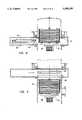
- the sealing of the pod 22 and loadlock chamberwill now be explained with reference to FIGS. 4, 4A and 5.
- the firstis within the pod 22.
- the pod cover 14 and pod door 23mate with each other, and a gasket 37 provided between the cover and door provides an isolating seal against the external environment.
- the second isolated environmentis defined by the purging chamber 28 (the purpose and operation of which shall be explained hereinafter).
- Gaskets 39 and 41are provided between the port plate assembly 21 and an upper surface of port access door 26, and between a lower surface of port access door 26 and operation chamber interior walls 31, respectively, to isolate and seal the purging chamber 28.
- the third isolated environment that exists when pod 22 is first located on the loadlock chamberis within interior operation chamber 30.
- Gasket 41provides a seal between the port access door 26 and the operation chamber 30 to isolate the interior of the chamber 30.
- gasket 37no longer provides a seal for the interior of the pod
- gasket 39no longer provides a seal for the interior of the purging chamber.
- the interior of the pod and the interior of the purging chambercomprise a single isolated environment that remains sealed against the external environment.
- the sealis accomplished by O-ring gasket 25 provided between the port plate assembly 21 and the pod cover 14. As previously explained, this seal is established when the pod 22 is located on the loadlock chamber 20. Additionally, as is known in the art, a seal is provided between the movable port plate assembly 21 and the purge chamber housing. Thus, the wafers within the cassette remain isolated from the external environment even after the pod cover 14 is separated from the pod door 23.
- Port access door 26is preferably formed of a non-reactive metal, and serves both to allow access to and to seal the interior of loadlock chamber 20.
- port access door 26is substantially circular, and has a diameter of approximately 15 inches. The thickness of the door 26 is approximately 1.5 inches. It is understood that port access door 26 may be configured to a different shape to conform to various configurations of the loadlock chamber.
- pod door 23 and port access door 26are moved laterally away from the loadlock chamber port access.
- the pod door and port access doormay be pivoted about a central axis away from the chamber port access.
- the movement of the port access dooris accomplished by means of a motor or jack screws (not shown) or other similar device, the operation of which is controlled by the CPU.
- the interior of the pod cover, the purging chamber, and the interior of the loadlock chamberall comprise a single environment that is isolated and sealed against the external environment.
- indexing platform 32is moved upward to engage the wafer cassette.
- the pawls 38a and 38bdisengage the cassette so that the cassette is decoupled from the port plate assembly 21 and fully supported on the indexing platform 32.
- a mechanical sensorfor example, may be provided within the platform to indicate when the indexing platform has engaged the wafer cassette.
- the wafer cassetteis aligned on the indexing platform 32 by means of extensions 40a, 40b, and 40c, which extensions are received within troughs 42a, 42b, and 42c on the bottom of the cassette 12.
- extensions 40a, 40b, and 40cwhich extensions are received within troughs 42a, 42b, and 42c on the bottom of the cassette 12.
- Indexing platform 32is supported and vertically translated by means of telescopic shaft 45, which extends down out of the bottom of the loadlock chamber.
- a motor or similar devicelocated below the chamber and which is controlled by the CPU, raises and lowers the telescopic shaft to the desired elevation.
- a conventional metal, accordion-type bellows 34is provided around the telescopic shaft 45 to provide a vacuum seal between the opening in the bottom of the chamber for the shaft 45 and the interior of the loadlock chamber. The bellows 34 expands and contracts along its length so as to always extend between the bottom of the interior operation chamber 30 and the bottom surface of the indexing platform 32.
- loadlock chamberpreferably has a cylindrical form factor, and the volume of the interior operation chamber 30 is approximately 3000 cubic inches, with an interior diameter of approximately 14 inches and a height of approximately 20 inches.
- the form factor, configuration and overall volume of the interior operation chamber 30may vary in alternative embodiments of the invention, as for example when wafers having diameters lesser or greater than 300 mm are used.
- the walls 31 surrounding the interior operation chamberare preferably formed of a non-reactive metal and have a wall thickness of approximately 0.25 to 0.375 inches. This relatively thin wall thickness provides the advantage of easier and less expensive chamber fabrication and also provides a loadlock chamber that is lighter than conventional loadlock chambers.
- a wafer cassette 12may be transferred directly from a pod 22 to the interior operation chamber 30 of loadlock chamber 20 without exposure to the atmosphere surrounding the pod or loadlock chamber.
- conventional systemsrequired that a wafer and wafer cassette be exposed to the atmosphere surrounding both the pod and loadlock chamber in order to transfer the wafer cassette from the pod to within the loadlock chamber.
- operation chamber 30is evacuated by means of a pump (not shown) to a pressure of approximately 10 -3 to 10 -8 Torr.
- a pumpnot shown
- any of several pumpsmay be used to accomplish the evacuation, such as for example a mechanical roughing pump or diffusion pump.
- wafers from the cassettemay be transferred to one or more high-vacuum wafer fabrication processes within processing chambers 44 (FIG. 10).
- a processing chamber 44may comprise, for example, a chemical vapor deposition, plasma etching, or other such high-vacuum process chamber.
- the final pressure at which the fabrication processes take place within the processing chambersmay be different than the evacuated pressure within the loadlock chamber.
- the pressuresmay be the same to prevent air currents and a circulation of any contaminants that may be in the chambers.
- the pressuremay be pumped up or down to the desired processing pressure.
- the pressure in the loadlock chambermay be slightly different than the pressure within the fabrication process chambers when the loadlock chamber is opened to the process chambers.
- loadlock chamber 20further includes access ports 36 for providing access by the wafers to the various fabrication processes taking place within processing chambers 44.
- the access portsmay be modular equipment standardization committee ("MESC") access ports or similar type access ports.
- An access port 36is closed when the cassette 12 is first lowered into the interior operation chamber 30, and opens to the process chambers after the interior operation chamber 30 is sealed and evacuated.
- the loadlock chamber 20 shown in FIG. 10includes one access port 36 connecting loadlock chamber 20 with the plurality of wafer processing chambers 44.
- a wafer transfer device 46is mounted within a main staging area 48 central to the various wafer processing chambers. Wafer transfer device 46 extends through access port 36 and into the wafer cassette to access a particular wafer 16.
- the wafer 16is withdrawn from the cassette, passed through the access port 36 and then transferred between the various wafer processing chambers. Upon completion of the various fabrication processes, the wafer transfer device 46 once again returns the wafer through the access port 36 and back to its position within the cassette 12.
- loadlock chamber 20may include more than one access port 36.
- a single loadlock chamber according to the present inventionmay allow access to a large number of wafer fabrication processes.
- indexing platform 32rotate within interior operation chamber 30 so as to align the front opening of the cassette with the various access ports 36.
- Indexing platform 32may be controlled by the CUP to rotate with respect to telescopic shaft 45. Alternatively, both the indexing platform and the shaft may be controlled to rotate together.
- the access ports 36may be provided at locations around the circumference of the loadlock chamber and also at different elevations.
- sensors within the platformsuch as sensor 80, may be provided to indicate the rotational orientation of the cassette, so as to allow proper alignment of an opening of the cassette with a particular access port.
- the cassettes 12may be provided so that a plurality of cassettes may be stacked one on top of another. As shown in FIG. 12, the loadlock chamber according to the present invention is provided to accommodate a plurality of such stacked cassettes 12. It is understood that in alternative embodiments, the height of loadlock chamber 20 may be increased to accommodate larger number of stacked cassettes. It is further contemplated that a first cassette 12 may be loaded into the interior operation chamber 30 as described above. Thereafter, with the first cassette 12 sealed within the operation chamber 30, the pod cover and pod door for the first cassette are moved away, and a second cassette 12 within a second pod 22 is loaded onto the loadlock chamber.
- the port access door and pod doormay be translated or pivoted away from the chamber access as described above, and the second cassette may be loaded on top of the first cassette within the chamber interior. In this way, a plurality of cassettes may be loaded into the loadlock chamber according to the present invention one at a time.
- the loadlock chambermay be provided with sensors 50 located on opposite sides of the cassette.
- sensors 50may record the exact vertical position of each wafer within the loadlock chamber.
- a wafer identifier and the absolute distance of the wafer from a surface of the indexing platemay be stored in the CPU memory.
- the precise vertical position of the indexing platformis known, the precise vertical position of the wafer within the loadlock chamber is known.
- Such informationis vital to accurate positioning of a particular wafer with respect to an access port 36 and with respect to a wafer transfer device 46. Additionally, as the precise vertical position of the indexing platform is known, the precise vertical position of the various cassette slots within a cassette are also known. This information is essential to accurate positioning a cassette slot with respect to a wafer that is to be inserted by the transfer device 46 into that slot. Also, sensors 50 allow any wafers which are "cross slotted", i.e., provided within the cassette on a slant, to be detected and corrected.
- wafer protrusion sensors 60may additionally be provided within the operation chamber 30 of the loadlock chamber to determine if a wafer is not fully seated within the cassette. While only one such sensor is shown in FIG. 12, more than one may be provided around the periphery of the chamber. As is known in the art, any of various sensing systems may be used as sensors 50 and 60, including a light or laser emitter and receiver.
- sensorsmay be provided to read information on the wafer such as a bar code, or to measure properties such as wafer film thickness and uniformity, surface roughness, moisture content, and film conductivity.
- sensorsmay be provided within the operation chamber 30 or within the access ports 36.
- Electrical leadsmay be provided through the chamber walls 31 to carry the signals from the various sensors to the CPU and/or to the CPU memory storage for future use.
- a section of the walls 31may be formed of a transparent material so that a sensor within the operation chamber 30 may be read from outside of the chamber.
- a wafermay be withdrawn from a particular location within a particular cassette by wafer transfer device 46, the vertical position of the cassette(s) within the chamber varied, and then reinserting the wafer into a cassette at a new location.
- a "good” wafer provided within a cassette including otherwise "bad” wafersmay be moved to a cassette including other good wafers.
- the pod 22is effective in preventing particulate contaminants from the surrounding environment from contacting the wafers.
- the present inventionincludes a gas purging feature shown in FIG. 13.
- a purging gasis injected through vent 52 whereafter it circulates within the pod cover and eventually exits through vent 54 in purging chamber 28.
- the purging gascan be conditioned prior to injection into the vent 52 to better remove contaminants from the pod.
- the gasmay be heated to evaporate and flush out vapor contaminants from the walls of the pod and purging chamber.
- Other ways of conditioning the purging gasinclude ionizing the gas and chemically filtering the gas.
- the purging operationmay be carried out during the majority of the loading and unloading sequence of the cassette to and from the operation chamber 30. Alternatively, this purging operation may be carried out after the wafer cassette is fully contained within the chamber 30, and the operation chamber is sealed by port access door 26. Any of various gasses may be used as the purging gas including relatively inert gasses such as nitrogen, noble gases such as argon, and chemically filtered air.
- the operation chamber 30 of the loadlock chamberis backfilled with gas in preparation for opening of port access door 26 and return of the wafer cassette to the pod.
- the chamber 30may preferably be backfilled with gasses similar to those used for the purging gas described above to minimize the possibility of exposure to ambient clean room air which may contain oxygen water vapor and other harmful molecular level contaminations.
Landscapes
- Engineering & Computer Science (AREA)
- Physics & Mathematics (AREA)
- Condensed Matter Physics & Semiconductors (AREA)
- General Physics & Mathematics (AREA)
- Manufacturing & Machinery (AREA)
- Computer Hardware Design (AREA)
- Microelectronics & Electronic Packaging (AREA)
- Power Engineering (AREA)
- Container, Conveyance, Adherence, Positioning, Of Wafer (AREA)
Abstract
Description
Claims (41)
Priority Applications (2)
| Application Number | Priority Date | Filing Date | Title |
|---|---|---|---|
| US08/394,698US5586585A (en) | 1995-02-27 | 1995-02-27 | Direct loadlock interface |
| PCT/US1996/002584WO1996026874A1 (en) | 1995-02-27 | 1996-02-27 | Standard mechanical interface integrated vacuum loadlock chamber |
Applications Claiming Priority (1)
| Application Number | Priority Date | Filing Date | Title |
|---|---|---|---|
| US08/394,698US5586585A (en) | 1995-02-27 | 1995-02-27 | Direct loadlock interface |
Publications (1)
| Publication Number | Publication Date |
|---|---|
| US5586585Atrue US5586585A (en) | 1996-12-24 |
Family
ID=23560052
Family Applications (1)
| Application Number | Title | Priority Date | Filing Date |
|---|---|---|---|
| US08/394,698Expired - LifetimeUS5586585A (en) | 1995-02-27 | 1995-02-27 | Direct loadlock interface |
Country Status (2)
| Country | Link |
|---|---|
| US (1) | US5586585A (en) |
| WO (1) | WO1996026874A1 (en) |
Cited By (411)
| Publication number | Priority date | Publication date | Assignee | Title |
|---|---|---|---|---|
| US5752796A (en)* | 1996-01-24 | 1998-05-19 | Muka; Richard S. | Vacuum integrated SMIF system |
| US5788458A (en)* | 1995-07-10 | 1998-08-04 | Asyst Technologies, Inc. | Method and apparatus for vertical transfer of a semiconductor wafer cassette |
| USD397346S (en) | 1997-07-16 | 1998-08-25 | Industrial Technology Research Institute | Wafer-boat positioning member of wafer container |
| US5836736A (en)* | 1994-04-28 | 1998-11-17 | Semitool, Inc. | Semiconductor processing system with wafer container docking and loading station |
| US5957648A (en)* | 1996-12-11 | 1999-09-28 | Applied Materials, Inc. | Factory automation apparatus and method for handling, moving and storing semiconductor wafer carriers |
| US5964561A (en)* | 1996-12-11 | 1999-10-12 | Applied Materials, Inc. | Compact apparatus and method for storing and loading semiconductor wafer carriers |
| US6048154A (en)* | 1996-10-02 | 2000-04-11 | Applied Materials, Inc. | High vacuum dual stage load lock and method for loading and unloading wafers using a high vacuum dual stage load lock |
| US6059507A (en)* | 1997-04-21 | 2000-05-09 | Brooks Automation, Inc. | Substrate processing apparatus with small batch load lock |
| US6082951A (en)* | 1998-01-23 | 2000-07-04 | Applied Materials, Inc. | Wafer cassette load station |
| US6106213A (en)* | 1998-02-27 | 2000-08-22 | Pri Automation, Inc. | Automated door assembly for use in semiconductor wafer manufacturing |
| US6120229A (en)* | 1999-02-01 | 2000-09-19 | Brooks Automation Inc. | Substrate carrier as batchloader |
| US6123494A (en)* | 1997-04-11 | 2000-09-26 | Leybold Systems Gmbh | Process for the loading and unloading of an evacuatable treatment chamber and handling device for carrying out the process |
| US6135168A (en)* | 1999-12-22 | 2000-10-24 | Industrial Technology Research Institute | Standard mechanical interface wafer pod gas filling system |
| US6142722A (en)* | 1998-06-17 | 2000-11-07 | Genmark Automation, Inc. | Automated opening and closing of ultra clean storage containers |
| US6152669A (en)* | 1995-11-13 | 2000-11-28 | Shinko Electric Co., Ltd. | Mechanical interface apparatus |
| US6234219B1 (en) | 1999-05-25 | 2001-05-22 | Micron Technology, Inc. | Liner for use in processing chamber |
| US6267158B1 (en)* | 1999-06-11 | 2001-07-31 | Sony Corporation | Sealed container, storage apparatus, electronic part conveyance system, and method of storage and conveyance of electronic parts |
| US6280134B1 (en)* | 1997-06-17 | 2001-08-28 | Applied Materials, Inc. | Apparatus and method for automated cassette handling |
| US6393334B1 (en) | 1999-02-12 | 2002-05-21 | Honeywell International Inc. | Method and apparatus for processing tool interface in a manufacturing environment |
| US6440261B1 (en) | 1999-05-25 | 2002-08-27 | Applied Materials, Inc. | Dual buffer chamber cluster tool for semiconductor wafer processing |
| US6494670B2 (en) | 1996-11-18 | 2002-12-17 | Applied Materials, Inc. | Three chamber load lock apparatus |
| US20030031537A1 (en)* | 2001-08-01 | 2003-02-13 | Semiconductor Leading Edge Technologies, Inc. | Load port, wafer processing apparatus, and method of replacing atmosphere |
| US20030031539A1 (en)* | 2000-03-16 | 2003-02-13 | Jaim Nulman | Apparatus for storing and moving a cassette |
| US6540466B2 (en) | 1996-12-11 | 2003-04-01 | Applied Materials, Inc. | Compact apparatus and method for storing and loading semiconductor wafer carriers |
| US6558509B2 (en) | 1999-11-30 | 2003-05-06 | Applied Materials, Inc. | Dual wafer load lock |
| US20030152445A1 (en)* | 2002-02-08 | 2003-08-14 | Takayuki Yamagishi | Semiconductor processing apparatus comprising chamber partitioned into reaction and transfer sections |
| US6688840B2 (en)* | 2001-05-02 | 2004-02-10 | Canon Kabushiki Kaisha | Transport apparatus and method |
| US6696367B1 (en)* | 2002-09-27 | 2004-02-24 | Asm America, Inc. | System for the improved handling of wafers within a process tool |
| US6704998B1 (en)* | 1997-12-24 | 2004-03-16 | Asyst Technologies, Inc. | Port door removal and wafer handling robotic system |
| US20040083955A1 (en)* | 2000-10-04 | 2004-05-06 | Ramsay Bruce Gordon | Vacuum chamber load lock structure and article transport mechanism |
| US20040118659A1 (en)* | 2002-12-20 | 2004-06-24 | Clinton Haris | Method and system for operating a semiconductor factory |
| US20040126206A1 (en)* | 2001-01-05 | 2004-07-01 | Tdk Corporation | Mini-environment system and operating method thereof |
| US6786935B1 (en)* | 2000-03-10 | 2004-09-07 | Applied Materials, Inc. | Vacuum processing system for producing components |
| US6821073B1 (en)* | 1999-07-09 | 2004-11-23 | Tokyo Electron Limited | Container handling system for substrate processing apparatus and method of handling containers |
| US6833035B1 (en) | 1994-04-28 | 2004-12-21 | Semitool, Inc. | Semiconductor processing system with wafer container docking and loading station |
| US20050069420A1 (en)* | 2003-09-25 | 2005-03-31 | Tdk Corporation | Purging system and purging method for the interior of a portable type hermetically sealed container |
| US20050118009A1 (en)* | 2003-11-10 | 2005-06-02 | Blueshift Technologies, Inc. | Stacked process modules for a semiconductor handling system |
| US20050150757A1 (en)* | 1997-03-17 | 2005-07-14 | Applied Komatsu Technology, Inc. | Heated and cooled vacuum chamber shield |
| US6949143B1 (en) | 1999-12-15 | 2005-09-27 | Applied Materials, Inc. | Dual substrate loadlock process equipment |
| US20050238475A1 (en)* | 2002-10-31 | 2005-10-27 | Randy Golden | System and method for stacking a predetermined number of nestable objects |
| US20050252571A1 (en)* | 2004-05-12 | 2005-11-17 | Ryuichi Nakano | Apparatus for replacing gas in storage container and method for replacing gas therewith |
| US7018504B1 (en)* | 2000-09-11 | 2006-03-28 | Asm America, Inc. | Loadlock with integrated pre-clean chamber |
| US7080652B2 (en) | 1994-04-28 | 2006-07-25 | Semitool, Inc. | Automated semiconductor processing systems |
| US7105463B2 (en) | 2000-09-15 | 2006-09-12 | Applied Materials, Inc. | Load lock chamber having two dual slot regions |
| US20060272169A1 (en)* | 2003-04-28 | 2006-12-07 | Toshihiko Miyajima | Purging apparatus and purging method |
| US7207766B2 (en) | 2003-10-20 | 2007-04-24 | Applied Materials, Inc. | Load lock chamber for large area substrate processing system |
| US20070138735A1 (en)* | 2005-12-15 | 2007-06-21 | Berger Gerald P | Enclosed carton magazine assembly |
| US20070267389A1 (en)* | 2006-05-18 | 2007-11-22 | Siegfried Straemke | Plasma treatment installation |
| US20070274810A1 (en)* | 2006-05-26 | 2007-11-29 | Holtkamp William H | Linearly distributed semiconductor workpiece processing tool |
| US7316966B2 (en) | 2001-09-21 | 2008-01-08 | Applied Materials, Inc. | Method for transferring substrates in a load lock chamber |
| US20080107508A1 (en)* | 2006-11-02 | 2008-05-08 | Chartered Semiconductor Manufacturing Ltd. | Wafer handling system for a loadlock |
| US20080152474A1 (en)* | 2005-02-22 | 2008-06-26 | Bart Scholte Van Mast | Method for Positioning a Wafer |
| US20080202416A1 (en)* | 2006-01-19 | 2008-08-28 | Provencher Timothy J | High temperature ALD inlet manifold |
| US7445415B2 (en) | 2005-02-24 | 2008-11-04 | Asyst Technologies, Inc. | Direct tool loading |
| US7497414B2 (en) | 2004-06-14 | 2009-03-03 | Applied Materials, Inc. | Curved slit valve door with flexible coupling |
| US20090060691A1 (en)* | 2007-08-28 | 2009-03-05 | Tokyo Electron Limited | Substrate receiving apparatus and substrate receiving method |
| US7523769B2 (en) | 2004-10-26 | 2009-04-28 | Tdk Corporation | Enclosed container lid opening/closing system and enclosed container lid opening/closing method |
| US20090129897A1 (en)* | 2007-05-09 | 2009-05-21 | Brooks Automation, Inc. | Side opening unified pod |
| US20090196714A1 (en)* | 2006-06-09 | 2009-08-06 | Raphael Sylvestre | Device for the transport, storage, and transfer of substrates |
| US20090219504A1 (en)* | 2004-10-26 | 2009-09-03 | Nikon Corporation | Substrate conveyor apparatus, substrate conveyance method and exposure apparatus |
| US7665951B2 (en) | 2006-06-02 | 2010-02-23 | Applied Materials, Inc. | Multiple slot load lock chamber and method of operation |
| US20100093181A1 (en)* | 2008-10-09 | 2010-04-15 | Asm Japan K.K. | Purge step-controlled sequence of processing semiconductor wafers |
| US20100098517A1 (en)* | 2008-10-16 | 2010-04-22 | Tokyo Electron Limited | Processing apparatus and processing method |
| US7723701B1 (en)* | 2005-07-29 | 2010-05-25 | South Bay Technology, Inc. | Specimen preservation systems and methods |
| US20100173432A1 (en)* | 2009-01-08 | 2010-07-08 | Asm America, Inc. | Gap maintenance for opening to process chamber |
| US20100190343A1 (en)* | 2009-01-28 | 2010-07-29 | Asm America, Inc. | Load lock having secondary isolation chamber |
| US20100202860A1 (en)* | 2009-02-09 | 2010-08-12 | Asm America, Inc. | Method and apparatus for minimizing contamination in semiconductor processing chamber |
| US7845618B2 (en) | 2006-06-28 | 2010-12-07 | Applied Materials, Inc. | Valve door with ball coupling |
| US7845891B2 (en) | 2006-01-13 | 2010-12-07 | Applied Materials, Inc. | Decoupled chamber body |
| US7857570B2 (en) | 2003-08-28 | 2010-12-28 | Applied Materials, Inc. | Method and apparatus for supplying substrates to a processing tool |
| US20110070055A1 (en)* | 2009-09-18 | 2011-03-24 | Tdk Corporation | Load port apparatus and dust exhaust method for load port apparatus |
| US7988399B2 (en) | 2003-11-10 | 2011-08-02 | Brooks Automation, Inc. | Mid-entry load lock for semiconductor handling system |
| US8124907B2 (en) | 2006-08-04 | 2012-02-28 | Applied Materials, Inc. | Load lock chamber with decoupled slit valve door seal compartment |
| US20120237323A1 (en)* | 2011-03-16 | 2012-09-20 | Tokyo Electron Limited | Lid opening and closing device |
| US8348583B2 (en) | 1999-10-19 | 2013-01-08 | Rorze Corporation | Container and loader for substrate |
| US8500388B2 (en) | 2003-11-10 | 2013-08-06 | Brooks Automation, Inc. | Semiconductor wafer handling and transport |
| US20150183538A1 (en)* | 2013-12-30 | 2015-07-02 | Sidel S.P.A. Con Socio Unico | Unit for carrying out an operation on a container fillable with a pourable product |
| JPWO2013187121A1 (en)* | 2012-06-14 | 2016-02-04 | 村田機械株式会社 | Lid opening / closing device |
| US9388492B2 (en) | 2011-12-27 | 2016-07-12 | Asm America, Inc. | Vapor flow control apparatus for atomic layer deposition |
| US9564350B1 (en)* | 2015-09-18 | 2017-02-07 | Globalfoundries Inc. | Method and apparatus for storing and transporting semiconductor wafers in a vacuum pod |
| US9574268B1 (en) | 2011-10-28 | 2017-02-21 | Asm America, Inc. | Pulsed valve manifold for atomic layer deposition |
| US20170170038A1 (en)* | 2015-12-14 | 2017-06-15 | Solarcity Corporation | Micro-environment container for photovoltaic cells |
| US20170221743A1 (en)* | 2016-02-02 | 2017-08-03 | Tokyo Electron Limited | Connecting mechanism and connecting method of substrate container |
| US20180130685A1 (en)* | 2016-11-10 | 2018-05-10 | Applied Materials, Inc. | Systems, apparatus, and methods for an improved load port |
| US20180174826A1 (en)* | 2016-12-15 | 2018-06-21 | Asm Ip Holding B.V. | Sequential infiltration synthesis apparatus |
| US10086511B2 (en) | 2003-11-10 | 2018-10-02 | Brooks Automation, Inc. | Semiconductor manufacturing systems |
| EP3312872A4 (en)* | 2015-06-19 | 2019-02-27 | Sinfonia Technology Co., Ltd. | CONTENT DISPLACEMENT DEVICE |
| US10559458B1 (en) | 2018-11-26 | 2020-02-11 | Asm Ip Holding B.V. | Method of forming oxynitride film |
| US10561975B2 (en) | 2014-10-07 | 2020-02-18 | Asm Ip Holdings B.V. | Variable conductance gas distribution apparatus and method |
| USD876504S1 (en) | 2017-04-03 | 2020-02-25 | Asm Ip Holding B.V. | Exhaust flow control ring for semiconductor deposition apparatus |
| US10590535B2 (en) | 2017-07-26 | 2020-03-17 | Asm Ip Holdings B.V. | Chemical treatment, deposition and/or infiltration apparatus and method for using the same |
| US10600673B2 (en) | 2015-07-07 | 2020-03-24 | Asm Ip Holding B.V. | Magnetic susceptor to baseplate seal |
| US10604847B2 (en) | 2014-03-18 | 2020-03-31 | Asm Ip Holding B.V. | Gas distribution system, reactor including the system, and methods of using the same |
| US10612136B2 (en) | 2018-06-29 | 2020-04-07 | ASM IP Holding, B.V. | Temperature-controlled flange and reactor system including same |
| US10622375B2 (en) | 2016-11-07 | 2020-04-14 | Asm Ip Holding B.V. | Method of processing a substrate and a device manufactured by using the method |
| US10643904B2 (en) | 2016-11-01 | 2020-05-05 | Asm Ip Holdings B.V. | Methods for forming a semiconductor device and related semiconductor device structures |
| US10643826B2 (en) | 2016-10-26 | 2020-05-05 | Asm Ip Holdings B.V. | Methods for thermally calibrating reaction chambers |
| US10655221B2 (en) | 2017-02-09 | 2020-05-19 | Asm Ip Holding B.V. | Method for depositing oxide film by thermal ALD and PEALD |
| US10658205B2 (en) | 2017-09-28 | 2020-05-19 | Asm Ip Holdings B.V. | Chemical dispensing apparatus and methods for dispensing a chemical to a reaction chamber |
| US10658181B2 (en) | 2018-02-20 | 2020-05-19 | Asm Ip Holding B.V. | Method of spacer-defined direct patterning in semiconductor fabrication |
| US10665452B2 (en) | 2016-05-02 | 2020-05-26 | Asm Ip Holdings B.V. | Source/drain performance through conformal solid state doping |
| US10662527B2 (en) | 2016-06-01 | 2020-05-26 | Asm Ip Holding B.V. | Manifolds for uniform vapor deposition |
| US10672636B2 (en) | 2017-08-09 | 2020-06-02 | Asm Ip Holding B.V. | Cassette holder assembly for a substrate cassette and holding member for use in such assembly |
| US10685834B2 (en) | 2017-07-05 | 2020-06-16 | Asm Ip Holdings B.V. | Methods for forming a silicon germanium tin layer and related semiconductor device structures |
| US10683571B2 (en) | 2014-02-25 | 2020-06-16 | Asm Ip Holding B.V. | Gas supply manifold and method of supplying gases to chamber using same |
| US10692741B2 (en) | 2017-08-08 | 2020-06-23 | Asm Ip Holdings B.V. | Radiation shield |
| US10707106B2 (en) | 2011-06-06 | 2020-07-07 | Asm Ip Holding B.V. | High-throughput semiconductor-processing apparatus equipped with multiple dual-chamber modules |
| US10714335B2 (en) | 2017-04-25 | 2020-07-14 | Asm Ip Holding B.V. | Method of depositing thin film and method of manufacturing semiconductor device |
| US10714350B2 (en) | 2016-11-01 | 2020-07-14 | ASM IP Holdings, B.V. | Methods for forming a transition metal niobium nitride film on a substrate by atomic layer deposition and related semiconductor device structures |
| US10714385B2 (en) | 2016-07-19 | 2020-07-14 | Asm Ip Holding B.V. | Selective deposition of tungsten |
| US10714315B2 (en) | 2012-10-12 | 2020-07-14 | Asm Ip Holdings B.V. | Semiconductor reaction chamber showerhead |
| US10720331B2 (en) | 2016-11-01 | 2020-07-21 | ASM IP Holdings, B.V. | Methods for forming a transition metal nitride film on a substrate by atomic layer deposition and related semiconductor device structures |
| US10720322B2 (en) | 2016-02-19 | 2020-07-21 | Asm Ip Holding B.V. | Method for forming silicon nitride film selectively on top surface |
| US10734244B2 (en) | 2017-11-16 | 2020-08-04 | Asm Ip Holding B.V. | Method of processing a substrate and a device manufactured by the same |
| US10731249B2 (en) | 2018-02-15 | 2020-08-04 | Asm Ip Holding B.V. | Method of forming a transition metal containing film on a substrate by a cyclical deposition process, a method for supplying a transition metal halide compound to a reaction chamber, and related vapor deposition apparatus |
| US10734223B2 (en) | 2017-10-10 | 2020-08-04 | Asm Ip Holding B.V. | Method for depositing a metal chalcogenide on a substrate by cyclical deposition |
| US10734497B2 (en) | 2017-07-18 | 2020-08-04 | Asm Ip Holding B.V. | Methods for forming a semiconductor device structure and related semiconductor device structures |
| US10741385B2 (en) | 2016-07-28 | 2020-08-11 | Asm Ip Holding B.V. | Method and apparatus for filling a gap |
| US10755923B2 (en) | 2018-07-03 | 2020-08-25 | Asm Ip Holding B.V. | Method for depositing silicon-free carbon-containing film as gap-fill layer by pulse plasma-assisted deposition |
| US10755922B2 (en) | 2018-07-03 | 2020-08-25 | Asm Ip Holding B.V. | Method for depositing silicon-free carbon-containing film as gap-fill layer by pulse plasma-assisted deposition |
| US10770286B2 (en) | 2017-05-08 | 2020-09-08 | Asm Ip Holdings B.V. | Methods for selectively forming a silicon nitride film on a substrate and related semiconductor device structures |
| US10767789B2 (en) | 2018-07-16 | 2020-09-08 | Asm Ip Holding B.V. | Diaphragm valves, valve components, and methods for forming valve components |
| US10770336B2 (en) | 2017-08-08 | 2020-09-08 | Asm Ip Holding B.V. | Substrate lift mechanism and reactor including same |
| US10784102B2 (en) | 2016-12-22 | 2020-09-22 | Asm Ip Holding B.V. | Method of forming a structure on a substrate |
| US10787741B2 (en) | 2014-08-21 | 2020-09-29 | Asm Ip Holding B.V. | Method and system for in situ formation of gas-phase compounds |
| US10797133B2 (en) | 2018-06-21 | 2020-10-06 | Asm Ip Holding B.V. | Method for depositing a phosphorus doped silicon arsenide film and related semiconductor device structures |
| US10804098B2 (en) | 2009-08-14 | 2020-10-13 | Asm Ip Holding B.V. | Systems and methods for thin-film deposition of metal oxides using excited nitrogen-oxygen species |
| US10811256B2 (en) | 2018-10-16 | 2020-10-20 | Asm Ip Holding B.V. | Method for etching a carbon-containing feature |
| US10818758B2 (en) | 2018-11-16 | 2020-10-27 | Asm Ip Holding B.V. | Methods for forming a metal silicate film on a substrate in a reaction chamber and related semiconductor device structures |
| USD900036S1 (en) | 2017-08-24 | 2020-10-27 | Asm Ip Holding B.V. | Heater electrical connector and adapter |
| US10832903B2 (en) | 2011-10-28 | 2020-11-10 | Asm Ip Holding B.V. | Process feed management for semiconductor substrate processing |
| US10829852B2 (en) | 2018-08-16 | 2020-11-10 | Asm Ip Holding B.V. | Gas distribution device for a wafer processing apparatus |
| US10847371B2 (en) | 2018-03-27 | 2020-11-24 | Asm Ip Holding B.V. | Method of forming an electrode on a substrate and a semiconductor device structure including an electrode |
| US10844486B2 (en) | 2009-04-06 | 2020-11-24 | Asm Ip Holding B.V. | Semiconductor processing reactor and components thereof |
| US10844484B2 (en) | 2017-09-22 | 2020-11-24 | Asm Ip Holding B.V. | Apparatus for dispensing a vapor phase reactant to a reaction chamber and related methods |
| US10847365B2 (en) | 2018-10-11 | 2020-11-24 | Asm Ip Holding B.V. | Method of forming conformal silicon carbide film by cyclic CVD |
| US10847366B2 (en) | 2018-11-16 | 2020-11-24 | Asm Ip Holding B.V. | Methods for depositing a transition metal chalcogenide film on a substrate by a cyclical deposition process |
| US10851456B2 (en) | 2016-04-21 | 2020-12-01 | Asm Ip Holding B.V. | Deposition of metal borides |
| USD903477S1 (en) | 2018-01-24 | 2020-12-01 | Asm Ip Holdings B.V. | Metal clamp |
| US10854498B2 (en) | 2011-07-15 | 2020-12-01 | Asm Ip Holding B.V. | Wafer-supporting device and method for producing same |
| US10858737B2 (en) | 2014-07-28 | 2020-12-08 | Asm Ip Holding B.V. | Showerhead assembly and components thereof |
| US10867788B2 (en) | 2016-12-28 | 2020-12-15 | Asm Ip Holding B.V. | Method of forming a structure on a substrate |
| US10865475B2 (en) | 2016-04-21 | 2020-12-15 | Asm Ip Holding B.V. | Deposition of metal borides and silicides |
| US10867786B2 (en) | 2018-03-30 | 2020-12-15 | Asm Ip Holding B.V. | Substrate processing method |
| US10872804B2 (en) | 2017-11-03 | 2020-12-22 | Asm Ip Holding B.V. | Apparatus and methods for isolating a reaction chamber from a loading chamber resulting in reduced contamination |
| US10872803B2 (en) | 2017-11-03 | 2020-12-22 | Asm Ip Holding B.V. | Apparatus and methods for isolating a reaction chamber from a loading chamber resulting in reduced contamination |
| US10872771B2 (en) | 2018-01-16 | 2020-12-22 | Asm Ip Holding B. V. | Method for depositing a material film on a substrate within a reaction chamber by a cyclical deposition process and related device structures |
| US10883175B2 (en) | 2018-08-09 | 2021-01-05 | Asm Ip Holding B.V. | Vertical furnace for processing substrates and a liner for use therein |
| US10892156B2 (en) | 2017-05-08 | 2021-01-12 | Asm Ip Holding B.V. | Methods for forming a silicon nitride film on a substrate and related semiconductor device structures |
| US10896820B2 (en) | 2018-02-14 | 2021-01-19 | Asm Ip Holding B.V. | Method for depositing a ruthenium-containing film on a substrate by a cyclical deposition process |
| US10910262B2 (en) | 2017-11-16 | 2021-02-02 | Asm Ip Holding B.V. | Method of selectively depositing a capping layer structure on a semiconductor device structure |
| US10914004B2 (en) | 2018-06-29 | 2021-02-09 | Asm Ip Holding B.V. | Thin-film deposition method and manufacturing method of semiconductor device |
| US10923344B2 (en) | 2017-10-30 | 2021-02-16 | Asm Ip Holding B.V. | Methods for forming a semiconductor structure and related semiconductor structures |
| US10928731B2 (en) | 2017-09-21 | 2021-02-23 | Asm Ip Holding B.V. | Method of sequential infiltration synthesis treatment of infiltrateable material and structures and devices formed using same |
| US10934619B2 (en) | 2016-11-15 | 2021-03-02 | Asm Ip Holding B.V. | Gas supply unit and substrate processing apparatus including the gas supply unit |
| US10941490B2 (en) | 2014-10-07 | 2021-03-09 | Asm Ip Holding B.V. | Multiple temperature range susceptor, assembly, reactor and system including the susceptor, and methods of using the same |
| USD913980S1 (en) | 2018-02-01 | 2021-03-23 | Asm Ip Holding B.V. | Gas supply plate for semiconductor manufacturing apparatus |
| US10975470B2 (en) | 2018-02-23 | 2021-04-13 | Asm Ip Holding B.V. | Apparatus for detecting or monitoring for a chemical precursor in a high temperature environment |
| US11001925B2 (en) | 2016-12-19 | 2021-05-11 | Asm Ip Holding B.V. | Substrate processing apparatus |
| US11004977B2 (en) | 2017-07-19 | 2021-05-11 | Asm Ip Holding B.V. | Method for depositing a group IV semiconductor and related semiconductor device structures |
| US11018047B2 (en) | 2018-01-25 | 2021-05-25 | Asm Ip Holding B.V. | Hybrid lift pin |
| US11015245B2 (en) | 2014-03-19 | 2021-05-25 | Asm Ip Holding B.V. | Gas-phase reactor and system having exhaust plenum and components thereof |
| US11018002B2 (en) | 2017-07-19 | 2021-05-25 | Asm Ip Holding B.V. | Method for selectively depositing a Group IV semiconductor and related semiconductor device structures |
| US11024523B2 (en) | 2018-09-11 | 2021-06-01 | Asm Ip Holding B.V. | Substrate processing apparatus and method |
| US11022879B2 (en) | 2017-11-24 | 2021-06-01 | Asm Ip Holding B.V. | Method of forming an enhanced unexposed photoresist layer |
| US11031242B2 (en) | 2018-11-07 | 2021-06-08 | Asm Ip Holding B.V. | Methods for depositing a boron doped silicon germanium film |
| USD922229S1 (en) | 2019-06-05 | 2021-06-15 | Asm Ip Holding B.V. | Device for controlling a temperature of a gas supply unit |
| US11049751B2 (en) | 2018-09-14 | 2021-06-29 | Asm Ip Holding B.V. | Cassette supply system to store and handle cassettes and processing apparatus equipped therewith |
| US11056344B2 (en) | 2017-08-30 | 2021-07-06 | Asm Ip Holding B.V. | Layer forming method |
| US11056567B2 (en) | 2018-05-11 | 2021-07-06 | Asm Ip Holding B.V. | Method of forming a doped metal carbide film on a substrate and related semiconductor device structures |
| US11053591B2 (en) | 2018-08-06 | 2021-07-06 | Asm Ip Holding B.V. | Multi-port gas injection system and reactor system including same |
| US11069510B2 (en) | 2017-08-30 | 2021-07-20 | Asm Ip Holding B.V. | Substrate processing apparatus |
| US11081345B2 (en) | 2018-02-06 | 2021-08-03 | Asm Ip Holding B.V. | Method of post-deposition treatment for silicon oxide film |
| US11088002B2 (en) | 2018-03-29 | 2021-08-10 | Asm Ip Holding B.V. | Substrate rack and a substrate processing system and method |
| US11087997B2 (en) | 2018-10-31 | 2021-08-10 | Asm Ip Holding B.V. | Substrate processing apparatus for processing substrates |
| US11094546B2 (en) | 2017-10-05 | 2021-08-17 | Asm Ip Holding B.V. | Method for selectively depositing a metallic film on a substrate |
| US11094582B2 (en) | 2016-07-08 | 2021-08-17 | Asm Ip Holding B.V. | Selective deposition method to form air gaps |
| US11101370B2 (en) | 2016-05-02 | 2021-08-24 | Asm Ip Holding B.V. | Method of forming a germanium oxynitride film |
| US11114294B2 (en) | 2019-03-08 | 2021-09-07 | Asm Ip Holding B.V. | Structure including SiOC layer and method of forming same |
| US11114283B2 (en) | 2018-03-16 | 2021-09-07 | Asm Ip Holding B.V. | Reactor, system including the reactor, and methods of manufacturing and using same |
| USD930782S1 (en) | 2019-08-22 | 2021-09-14 | Asm Ip Holding B.V. | Gas distributor |
| US11127589B2 (en) | 2019-02-01 | 2021-09-21 | Asm Ip Holding B.V. | Method of topology-selective film formation of silicon oxide |
| US11127617B2 (en) | 2017-11-27 | 2021-09-21 | Asm Ip Holding B.V. | Storage device for storing wafer cassettes for use with a batch furnace |
| USD931978S1 (en) | 2019-06-27 | 2021-09-28 | Asm Ip Holding B.V. | Showerhead vacuum transport |
| US11139191B2 (en) | 2017-08-09 | 2021-10-05 | Asm Ip Holding B.V. | Storage apparatus for storing cassettes for substrates and processing apparatus equipped therewith |
| US11139308B2 (en) | 2015-12-29 | 2021-10-05 | Asm Ip Holding B.V. | Atomic layer deposition of III-V compounds to form V-NAND devices |
| US11158513B2 (en) | 2018-12-13 | 2021-10-26 | Asm Ip Holding B.V. | Methods for forming a rhenium-containing film on a substrate by a cyclical deposition process and related semiconductor device structures |
| USD935572S1 (en) | 2019-05-24 | 2021-11-09 | Asm Ip Holding B.V. | Gas channel plate |
| US11171025B2 (en) | 2019-01-22 | 2021-11-09 | Asm Ip Holding B.V. | Substrate processing device |
| US11205585B2 (en) | 2016-07-28 | 2021-12-21 | Asm Ip Holding B.V. | Substrate processing apparatus and method of operating the same |
| US11217444B2 (en) | 2018-11-30 | 2022-01-04 | Asm Ip Holding B.V. | Method for forming an ultraviolet radiation responsive metal oxide-containing film |
| USD940837S1 (en) | 2019-08-22 | 2022-01-11 | Asm Ip Holding B.V. | Electrode |
| US11222772B2 (en) | 2016-12-14 | 2022-01-11 | Asm Ip Holding B.V. | Substrate processing apparatus |
| US11227789B2 (en) | 2019-02-20 | 2022-01-18 | Asm Ip Holding B.V. | Method and apparatus for filling a recess formed within a substrate surface |
| US11227782B2 (en) | 2019-07-31 | 2022-01-18 | Asm Ip Holding B.V. | Vertical batch furnace assembly |
| US11230766B2 (en) | 2018-03-29 | 2022-01-25 | Asm Ip Holding B.V. | Substrate processing apparatus and method |
| US11233133B2 (en) | 2015-10-21 | 2022-01-25 | Asm Ip Holding B.V. | NbMC layers |
| US11232963B2 (en) | 2018-10-03 | 2022-01-25 | Asm Ip Holding B.V. | Substrate processing apparatus and method |
| US11242598B2 (en) | 2015-06-26 | 2022-02-08 | Asm Ip Holding B.V. | Structures including metal carbide material, devices including the structures, and methods of forming same |
| US11251068B2 (en) | 2018-10-19 | 2022-02-15 | Asm Ip Holding B.V. | Substrate processing apparatus and substrate processing method |
| US11251040B2 (en) | 2019-02-20 | 2022-02-15 | Asm Ip Holding B.V. | Cyclical deposition method including treatment step and apparatus for same |
| USD944946S1 (en) | 2019-06-14 | 2022-03-01 | Asm Ip Holding B.V. | Shower plate |
| US11270899B2 (en) | 2018-06-04 | 2022-03-08 | Asm Ip Holding B.V. | Wafer handling chamber with moisture reduction |
| US11274369B2 (en) | 2018-09-11 | 2022-03-15 | Asm Ip Holding B.V. | Thin film deposition method |
| US11282698B2 (en) | 2019-07-19 | 2022-03-22 | Asm Ip Holding B.V. | Method of forming topology-controlled amorphous carbon polymer film |
| US11286562B2 (en) | 2018-06-08 | 2022-03-29 | Asm Ip Holding B.V. | Gas-phase chemical reactor and method of using same |
| US11289326B2 (en) | 2019-05-07 | 2022-03-29 | Asm Ip Holding B.V. | Method for reforming amorphous carbon polymer film |
| US11286558B2 (en) | 2019-08-23 | 2022-03-29 | Asm Ip Holding B.V. | Methods for depositing a molybdenum nitride film on a surface of a substrate by a cyclical deposition process and related semiconductor device structures including a molybdenum nitride film |
| US11295980B2 (en) | 2017-08-30 | 2022-04-05 | Asm Ip Holding B.V. | Methods for depositing a molybdenum metal film over a dielectric surface of a substrate by a cyclical deposition process and related semiconductor device structures |
| USD947913S1 (en) | 2019-05-17 | 2022-04-05 | Asm Ip Holding B.V. | Susceptor shaft |
| USD948463S1 (en) | 2018-10-24 | 2022-04-12 | Asm Ip Holding B.V. | Susceptor for semiconductor substrate supporting apparatus |
| USD949319S1 (en) | 2019-08-22 | 2022-04-19 | Asm Ip Holding B.V. | Exhaust duct |
| US11306395B2 (en) | 2017-06-28 | 2022-04-19 | Asm Ip Holding B.V. | Methods for depositing a transition metal nitride film on a substrate by atomic layer deposition and related deposition apparatus |
| US11315794B2 (en) | 2019-10-21 | 2022-04-26 | Asm Ip Holding B.V. | Apparatus and methods for selectively etching films |
| US11339476B2 (en) | 2019-10-08 | 2022-05-24 | Asm Ip Holding B.V. | Substrate processing device having connection plates, substrate processing method |
| US11342216B2 (en) | 2019-02-20 | 2022-05-24 | Asm Ip Holding B.V. | Cyclical deposition method and apparatus for filling a recess formed within a substrate surface |
| US11345999B2 (en) | 2019-06-06 | 2022-05-31 | Asm Ip Holding B.V. | Method of using a gas-phase reactor system including analyzing exhausted gas |
| US11355338B2 (en) | 2019-05-10 | 2022-06-07 | Asm Ip Holding B.V. | Method of depositing material onto a surface and structure formed according to the method |
| US11361990B2 (en) | 2018-05-28 | 2022-06-14 | Asm Ip Holding B.V. | Substrate processing method and device manufactured by using the same |
| US11374112B2 (en) | 2017-07-19 | 2022-06-28 | Asm Ip Holding B.V. | Method for depositing a group IV semiconductor and related semiconductor device structures |
| US11378337B2 (en)* | 2019-03-28 | 2022-07-05 | Asm Ip Holding B.V. | Door opener and substrate processing apparatus provided therewith |
| US11390946B2 (en) | 2019-01-17 | 2022-07-19 | Asm Ip Holding B.V. | Methods of forming a transition metal containing film on a substrate by a cyclical deposition process |
| US11393690B2 (en) | 2018-01-19 | 2022-07-19 | Asm Ip Holding B.V. | Deposition method |
| US11390945B2 (en) | 2019-07-03 | 2022-07-19 | Asm Ip Holding B.V. | Temperature control assembly for substrate processing apparatus and method of using same |
| US11390950B2 (en) | 2017-01-10 | 2022-07-19 | Asm Ip Holding B.V. | Reactor system and method to reduce residue buildup during a film deposition process |
| US11401605B2 (en) | 2019-11-26 | 2022-08-02 | Asm Ip Holding B.V. | Substrate processing apparatus |
| US11410851B2 (en) | 2017-02-15 | 2022-08-09 | Asm Ip Holding B.V. | Methods for forming a metallic film on a substrate by cyclical deposition and related semiconductor device structures |
| US11414760B2 (en) | 2018-10-08 | 2022-08-16 | Asm Ip Holding B.V. | Substrate support unit, thin film deposition apparatus including the same, and substrate processing apparatus including the same |
| US11424119B2 (en) | 2019-03-08 | 2022-08-23 | Asm Ip Holding B.V. | Method for selective deposition of silicon nitride layer and structure including selectively-deposited silicon nitride layer |
| US11430640B2 (en) | 2019-07-30 | 2022-08-30 | Asm Ip Holding B.V. | Substrate processing apparatus |
| US11430674B2 (en) | 2018-08-22 | 2022-08-30 | Asm Ip Holding B.V. | Sensor array, apparatus for dispensing a vapor phase reactant to a reaction chamber and related methods |
| US11437241B2 (en) | 2020-04-08 | 2022-09-06 | Asm Ip Holding B.V. | Apparatus and methods for selectively etching silicon oxide films |
| US11443926B2 (en) | 2019-07-30 | 2022-09-13 | Asm Ip Holding B.V. | Substrate processing apparatus |
| US11447864B2 (en) | 2019-04-19 | 2022-09-20 | Asm Ip Holding B.V. | Layer forming method and apparatus |
| US11447861B2 (en) | 2016-12-15 | 2022-09-20 | Asm Ip Holding B.V. | Sequential infiltration synthesis apparatus and a method of forming a patterned structure |
| US11453943B2 (en) | 2016-05-25 | 2022-09-27 | Asm Ip Holding B.V. | Method for forming carbon-containing silicon/metal oxide or nitride film by ALD using silicon precursor and hydrocarbon precursor |
| USD965044S1 (en) | 2019-08-19 | 2022-09-27 | Asm Ip Holding B.V. | Susceptor shaft |
| USD965524S1 (en) | 2019-08-19 | 2022-10-04 | Asm Ip Holding B.V. | Susceptor support |
| US11469098B2 (en) | 2018-05-08 | 2022-10-11 | Asm Ip Holding B.V. | Methods for depositing an oxide film on a substrate by a cyclical deposition process and related device structures |
| US11476109B2 (en) | 2019-06-11 | 2022-10-18 | Asm Ip Holding B.V. | Method of forming an electronic structure using reforming gas, system for performing the method, and structure formed using the method |
| US11473195B2 (en) | 2018-03-01 | 2022-10-18 | Asm Ip Holding B.V. | Semiconductor processing apparatus and a method for processing a substrate |
| US11482412B2 (en) | 2018-01-19 | 2022-10-25 | Asm Ip Holding B.V. | Method for depositing a gap-fill layer by plasma-assisted deposition |
| US11482418B2 (en) | 2018-02-20 | 2022-10-25 | Asm Ip Holding B.V. | Substrate processing method and apparatus |
| US11482533B2 (en) | 2019-02-20 | 2022-10-25 | Asm Ip Holding B.V. | Apparatus and methods for plug fill deposition in 3-D NAND applications |
| US11488854B2 (en) | 2020-03-11 | 2022-11-01 | Asm Ip Holding B.V. | Substrate handling device with adjustable joints |
| US11488819B2 (en) | 2018-12-04 | 2022-11-01 | Asm Ip Holding B.V. | Method of cleaning substrate processing apparatus |
| US11495459B2 (en) | 2019-09-04 | 2022-11-08 | Asm Ip Holding B.V. | Methods for selective deposition using a sacrificial capping layer |
| US11492701B2 (en) | 2019-03-19 | 2022-11-08 | Asm Ip Holding B.V. | Reactor manifolds |
| US11492703B2 (en) | 2018-06-27 | 2022-11-08 | Asm Ip Holding B.V. | Cyclic deposition methods for forming metal-containing material and films and structures including the metal-containing material |
| US11499222B2 (en) | 2018-06-27 | 2022-11-15 | Asm Ip Holding B.V. | Cyclic deposition methods for forming metal-containing material and films and structures including the metal-containing material |
| US11501968B2 (en) | 2019-11-15 | 2022-11-15 | Asm Ip Holding B.V. | Method for providing a semiconductor device with silicon filled gaps |
| US11499226B2 (en) | 2018-11-02 | 2022-11-15 | Asm Ip Holding B.V. | Substrate supporting unit and a substrate processing device including the same |
| US11515187B2 (en) | 2020-05-01 | 2022-11-29 | Asm Ip Holding B.V. | Fast FOUP swapping with a FOUP handler |
| US11515188B2 (en) | 2019-05-16 | 2022-11-29 | Asm Ip Holding B.V. | Wafer boat handling device, vertical batch furnace and method |
| US11521851B2 (en) | 2020-02-03 | 2022-12-06 | Asm Ip Holding B.V. | Method of forming structures including a vanadium or indium layer |
| US11527403B2 (en) | 2019-12-19 | 2022-12-13 | Asm Ip Holding B.V. | Methods for filling a gap feature on a substrate surface and related semiconductor structures |
| US11527400B2 (en) | 2019-08-23 | 2022-12-13 | Asm Ip Holding B.V. | Method for depositing silicon oxide film having improved quality by peald using bis(diethylamino)silane |
| US11530483B2 (en) | 2018-06-21 | 2022-12-20 | Asm Ip Holding B.V. | Substrate processing system |
| US11532757B2 (en) | 2016-10-27 | 2022-12-20 | Asm Ip Holding B.V. | Deposition of charge trapping layers |
| US11530876B2 (en) | 2020-04-24 | 2022-12-20 | Asm Ip Holding B.V. | Vertical batch furnace assembly comprising a cooling gas supply |
| US11551912B2 (en) | 2020-01-20 | 2023-01-10 | Asm Ip Holding B.V. | Method of forming thin film and method of modifying surface of thin film |
| US11551925B2 (en) | 2019-04-01 | 2023-01-10 | Asm Ip Holding B.V. | Method for manufacturing a semiconductor device |
| USD975665S1 (en) | 2019-05-17 | 2023-01-17 | Asm Ip Holding B.V. | Susceptor shaft |
| US11557474B2 (en) | 2019-07-29 | 2023-01-17 | Asm Ip Holding B.V. | Methods for selective deposition utilizing n-type dopants and/or alternative dopants to achieve high dopant incorporation |
| US11562901B2 (en) | 2019-09-25 | 2023-01-24 | Asm Ip Holding B.V. | Substrate processing method |
| US11572620B2 (en) | 2018-11-06 | 2023-02-07 | Asm Ip Holding B.V. | Methods for selectively depositing an amorphous silicon film on a substrate |
| US11587814B2 (en) | 2019-07-31 | 2023-02-21 | Asm Ip Holding B.V. | Vertical batch furnace assembly |
| US11587815B2 (en) | 2019-07-31 | 2023-02-21 | Asm Ip Holding B.V. | Vertical batch furnace assembly |
| USD979506S1 (en) | 2019-08-22 | 2023-02-28 | Asm Ip Holding B.V. | Insulator |
| US11594600B2 (en) | 2019-11-05 | 2023-02-28 | Asm Ip Holding B.V. | Structures with doped semiconductor layers and methods and systems for forming same |
| US11594450B2 (en) | 2019-08-22 | 2023-02-28 | Asm Ip Holding B.V. | Method for forming a structure with a hole |
| USD980814S1 (en) | 2021-05-11 | 2023-03-14 | Asm Ip Holding B.V. | Gas distributor for substrate processing apparatus |
| USD980813S1 (en) | 2021-05-11 | 2023-03-14 | Asm Ip Holding B.V. | Gas flow control plate for substrate processing apparatus |
| US11605528B2 (en) | 2019-07-09 | 2023-03-14 | Asm Ip Holding B.V. | Plasma device using coaxial waveguide, and substrate treatment method |
| US11610775B2 (en) | 2016-07-28 | 2023-03-21 | Asm Ip Holding B.V. | Method and apparatus for filling a gap |
| US11610774B2 (en) | 2019-10-02 | 2023-03-21 | Asm Ip Holding B.V. | Methods for forming a topographically selective silicon oxide film by a cyclical plasma-enhanced deposition process |
| US11615970B2 (en) | 2019-07-17 | 2023-03-28 | Asm Ip Holding B.V. | Radical assist ignition plasma system and method |
| USD981973S1 (en) | 2021-05-11 | 2023-03-28 | Asm Ip Holding B.V. | Reactor wall for substrate processing apparatus |
| US11626308B2 (en) | 2020-05-13 | 2023-04-11 | Asm Ip Holding B.V. | Laser alignment fixture for a reactor system |
| US11626316B2 (en) | 2019-11-20 | 2023-04-11 | Asm Ip Holding B.V. | Method of depositing carbon-containing material on a surface of a substrate, structure formed using the method, and system for forming the structure |
| US11629406B2 (en) | 2018-03-09 | 2023-04-18 | Asm Ip Holding B.V. | Semiconductor processing apparatus comprising one or more pyrometers for measuring a temperature of a substrate during transfer of the substrate |
| US11629407B2 (en) | 2019-02-22 | 2023-04-18 | Asm Ip Holding B.V. | Substrate processing apparatus and method for processing substrates |
| US11637014B2 (en) | 2019-10-17 | 2023-04-25 | Asm Ip Holding B.V. | Methods for selective deposition of doped semiconductor material |
| US11637011B2 (en) | 2019-10-16 | 2023-04-25 | Asm Ip Holding B.V. | Method of topology-selective film formation of silicon oxide |
| US11639548B2 (en) | 2019-08-21 | 2023-05-02 | Asm Ip Holding B.V. | Film-forming material mixed-gas forming device and film forming device |
| US11639811B2 (en) | 2017-11-27 | 2023-05-02 | Asm Ip Holding B.V. | Apparatus including a clean mini environment |
| US11646204B2 (en) | 2020-06-24 | 2023-05-09 | Asm Ip Holding B.V. | Method for forming a layer provided with silicon |
| US11643724B2 (en) | 2019-07-18 | 2023-05-09 | Asm Ip Holding B.V. | Method of forming structures using a neutral beam |
| US11646184B2 (en) | 2019-11-29 | 2023-05-09 | Asm Ip Holding B.V. | Substrate processing apparatus |
| US11644758B2 (en) | 2020-07-17 | 2023-05-09 | Asm Ip Holding B.V. | Structures and methods for use in photolithography |
| US11646205B2 (en) | 2019-10-29 | 2023-05-09 | Asm Ip Holding B.V. | Methods of selectively forming n-type doped material on a surface, systems for selectively forming n-type doped material, and structures formed using same |
| US11649546B2 (en) | 2016-07-08 | 2023-05-16 | Asm Ip Holding B.V. | Organic reactants for atomic layer deposition |
| US11658030B2 (en) | 2017-03-29 | 2023-05-23 | Asm Ip Holding B.V. | Method for forming doped metal oxide films on a substrate by cyclical deposition and related semiconductor device structures |
| US11658029B2 (en) | 2018-12-14 | 2023-05-23 | Asm Ip Holding B.V. | Method of forming a device structure using selective deposition of gallium nitride and system for same |
| US11658035B2 (en) | 2020-06-30 | 2023-05-23 | Asm Ip Holding B.V. | Substrate processing method |
| US11664245B2 (en) | 2019-07-16 | 2023-05-30 | Asm Ip Holding B.V. | Substrate processing device |
| US11664267B2 (en) | 2019-07-10 | 2023-05-30 | Asm Ip Holding B.V. | Substrate support assembly and substrate processing device including the same |
| US11664199B2 (en) | 2018-10-19 | 2023-05-30 | Asm Ip Holding B.V. | Substrate processing apparatus and substrate processing method |
| US11674220B2 (en) | 2020-07-20 | 2023-06-13 | Asm Ip Holding B.V. | Method for depositing molybdenum layers using an underlayer |
| US11680839B2 (en) | 2019-08-05 | 2023-06-20 | Asm Ip Holding B.V. | Liquid level sensor for a chemical source vessel |
| USD990534S1 (en) | 2020-09-11 | 2023-06-27 | Asm Ip Holding B.V. | Weighted lift pin |
| USD990441S1 (en) | 2021-09-07 | 2023-06-27 | Asm Ip Holding B.V. | Gas flow control plate |
| US11688603B2 (en) | 2019-07-17 | 2023-06-27 | Asm Ip Holding B.V. | Methods of forming silicon germanium structures |
| US11685991B2 (en) | 2018-02-14 | 2023-06-27 | Asm Ip Holding B.V. | Method for depositing a ruthenium-containing film on a substrate by a cyclical deposition process |
| US11705333B2 (en) | 2020-05-21 | 2023-07-18 | Asm Ip Holding B.V. | Structures including multiple carbon layers and methods of forming and using same |
| US11718913B2 (en) | 2018-06-04 | 2023-08-08 | Asm Ip Holding B.V. | Gas distribution system and reactor system including same |
| US11725277B2 (en) | 2011-07-20 | 2023-08-15 | Asm Ip Holding B.V. | Pressure transmitter for a semiconductor processing environment |
| US11725280B2 (en) | 2020-08-26 | 2023-08-15 | Asm Ip Holding B.V. | Method for forming metal silicon oxide and metal silicon oxynitride layers |
| US11735422B2 (en) | 2019-10-10 | 2023-08-22 | Asm Ip Holding B.V. | Method of forming a photoresist underlayer and structure including same |
| US11742189B2 (en) | 2015-03-12 | 2023-08-29 | Asm Ip Holding B.V. | Multi-zone reactor, system including the reactor, and method of using the same |
| US11742198B2 (en) | 2019-03-08 | 2023-08-29 | Asm Ip Holding B.V. | Structure including SiOCN layer and method of forming same |
| US11767589B2 (en) | 2020-05-29 | 2023-09-26 | Asm Ip Holding B.V. | Substrate processing device |
| US11769682B2 (en) | 2017-08-09 | 2023-09-26 | Asm Ip Holding B.V. | Storage apparatus for storing cassettes for substrates and processing apparatus equipped therewith |
| US11776846B2 (en) | 2020-02-07 | 2023-10-03 | Asm Ip Holding B.V. | Methods for depositing gap filling fluids and related systems and devices |
| US11781221B2 (en) | 2019-05-07 | 2023-10-10 | Asm Ip Holding B.V. | Chemical source vessel with dip tube |
| US11781243B2 (en) | 2020-02-17 | 2023-10-10 | Asm Ip Holding B.V. | Method for depositing low temperature phosphorous-doped silicon |
| US11804364B2 (en) | 2020-05-19 | 2023-10-31 | Asm Ip Holding B.V. | Substrate processing apparatus |
| US11814747B2 (en) | 2019-04-24 | 2023-11-14 | Asm Ip Holding B.V. | Gas-phase reactor system-with a reaction chamber, a solid precursor source vessel, a gas distribution system, and a flange assembly |
| US11823876B2 (en) | 2019-09-05 | 2023-11-21 | Asm Ip Holding B.V. | Substrate processing apparatus |
| US11821078B2 (en) | 2020-04-15 | 2023-11-21 | Asm Ip Holding B.V. | Method for forming precoat film and method for forming silicon-containing film |
| US11823866B2 (en) | 2020-04-02 | 2023-11-21 | Asm Ip Holding B.V. | Thin film forming method |
| US11828707B2 (en) | 2020-02-04 | 2023-11-28 | Asm Ip Holding B.V. | Method and apparatus for transmittance measurements of large articles |
| US11827981B2 (en) | 2020-10-14 | 2023-11-28 | Asm Ip Holding B.V. | Method of depositing material on stepped structure |
| US11830738B2 (en) | 2020-04-03 | 2023-11-28 | Asm Ip Holding B.V. | Method for forming barrier layer and method for manufacturing semiconductor device |
| US11830730B2 (en) | 2017-08-29 | 2023-11-28 | Asm Ip Holding B.V. | Layer forming method and apparatus |
| US11830731B2 (en) | 2019-10-22 | 2023-11-28 | Asm Ip Holding B.V. | Semiconductor deposition reactor manifolds |
| US11840761B2 (en) | 2019-12-04 | 2023-12-12 | Asm Ip Holding B.V. | Substrate processing apparatus |
| US11876356B2 (en) | 2020-03-11 | 2024-01-16 | Asm Ip Holding B.V. | Lockout tagout assembly and system and method of using same |
| US11873557B2 (en) | 2020-10-22 | 2024-01-16 | Asm Ip Holding B.V. | Method of depositing vanadium metal |
| US11885013B2 (en) | 2019-12-17 | 2024-01-30 | Asm Ip Holding B.V. | Method of forming vanadium nitride layer and structure including the vanadium nitride layer |
| USD1012873S1 (en) | 2020-09-24 | 2024-01-30 | Asm Ip Holding B.V. | Electrode for semiconductor processing apparatus |
| US11887857B2 (en) | 2020-04-24 | 2024-01-30 | Asm Ip Holding B.V. | Methods and systems for depositing a layer comprising vanadium, nitrogen, and a further element |
| US11885020B2 (en) | 2020-12-22 | 2024-01-30 | Asm Ip Holding B.V. | Transition metal deposition method |
| US11885023B2 (en) | 2018-10-01 | 2024-01-30 | Asm Ip Holding B.V. | Substrate retaining apparatus, system including the apparatus, and method of using same |
| US11891696B2 (en) | 2020-11-30 | 2024-02-06 | Asm Ip Holding B.V. | Injector configured for arrangement within a reaction chamber of a substrate processing apparatus |
| US11901179B2 (en) | 2020-10-28 | 2024-02-13 | Asm Ip Holding B.V. | Method and device for depositing silicon onto substrates |
| US11898243B2 (en) | 2020-04-24 | 2024-02-13 | Asm Ip Holding B.V. | Method of forming vanadium nitride-containing layer |
| US11915929B2 (en) | 2019-11-26 | 2024-02-27 | Asm Ip Holding B.V. | Methods for selectively forming a target film on a substrate comprising a first dielectric surface and a second metallic surface |
| US11923181B2 (en) | 2019-11-29 | 2024-03-05 | Asm Ip Holding B.V. | Substrate processing apparatus for minimizing the effect of a filling gas during substrate processing |
| US11929251B2 (en) | 2019-12-02 | 2024-03-12 | Asm Ip Holding B.V. | Substrate processing apparatus having electrostatic chuck and substrate processing method |
| US11946137B2 (en) | 2020-12-16 | 2024-04-02 | Asm Ip Holding B.V. | Runout and wobble measurement fixtures |
| US11959168B2 (en) | 2020-04-29 | 2024-04-16 | Asm Ip Holding B.V. | Solid source precursor vessel |
| US11961741B2 (en) | 2020-03-12 | 2024-04-16 | Asm Ip Holding B.V. | Method for fabricating layer structure having target topological profile |
| USD1023959S1 (en) | 2021-05-11 | 2024-04-23 | Asm Ip Holding B.V. | Electrode for substrate processing apparatus |
| US11967488B2 (en) | 2013-02-01 | 2024-04-23 | Asm Ip Holding B.V. | Method for treatment of deposition reactor |
| US11976359B2 (en) | 2020-01-06 | 2024-05-07 | Asm Ip Holding B.V. | Gas supply assembly, components thereof, and reactor system including same |
| US11987881B2 (en) | 2020-05-22 | 2024-05-21 | Asm Ip Holding B.V. | Apparatus for depositing thin films using hydrogen peroxide |
| US11986868B2 (en) | 2020-02-28 | 2024-05-21 | Asm Ip Holding B.V. | System dedicated for parts cleaning |
| US11996309B2 (en) | 2019-05-16 | 2024-05-28 | Asm Ip Holding B.V. | Wafer boat handling device, vertical batch furnace and method |
| US11996292B2 (en) | 2019-10-25 | 2024-05-28 | Asm Ip Holding B.V. | Methods for filling a gap feature on a substrate surface and related semiconductor structures |
| US11993843B2 (en) | 2017-08-31 | 2024-05-28 | Asm Ip Holding B.V. | Substrate processing apparatus |
| US11993847B2 (en) | 2020-01-08 | 2024-05-28 | Asm Ip Holding B.V. | Injector |
| US11996289B2 (en) | 2020-04-16 | 2024-05-28 | Asm Ip Holding B.V. | Methods of forming structures including silicon germanium and silicon layers, devices formed using the methods, and systems for performing the methods |
| US12009224B2 (en) | 2020-09-29 | 2024-06-11 | Asm Ip Holding B.V. | Apparatus and method for etching metal nitrides |
| US12006572B2 (en) | 2019-10-08 | 2024-06-11 | Asm Ip Holding B.V. | Reactor system including a gas distribution assembly for use with activated species and method of using same |
| US12009241B2 (en) | 2019-10-14 | 2024-06-11 | Asm Ip Holding B.V. | Vertical batch furnace assembly with detector to detect cassette |
| US12020934B2 (en) | 2020-07-08 | 2024-06-25 | Asm Ip Holding B.V. | Substrate processing method |
| US12025484B2 (en) | 2018-05-08 | 2024-07-02 | Asm Ip Holding B.V. | Thin film forming method |
| US12027365B2 (en) | 2020-11-24 | 2024-07-02 | Asm Ip Holding B.V. | Methods for filling a gap and related systems and devices |
| US12033885B2 (en) | 2020-01-06 | 2024-07-09 | Asm Ip Holding B.V. | Channeled lift pin |
| US12040200B2 (en) | 2017-06-20 | 2024-07-16 | Asm Ip Holding B.V. | Semiconductor processing apparatus and methods for calibrating a semiconductor processing apparatus |
| US12040177B2 (en) | 2020-08-18 | 2024-07-16 | Asm Ip Holding B.V. | Methods for forming a laminate film by cyclical plasma-enhanced deposition processes |
| US12040199B2 (en) | 2018-11-28 | 2024-07-16 | Asm Ip Holding B.V. | Substrate processing apparatus for processing substrates |
| US12051602B2 (en) | 2020-05-04 | 2024-07-30 | Asm Ip Holding B.V. | Substrate processing system for processing substrates with an electronics module located behind a door in a front wall of the substrate processing system |
| US12051567B2 (en) | 2020-10-07 | 2024-07-30 | Asm Ip Holding B.V. | Gas supply unit and substrate processing apparatus including gas supply unit |
| US12057314B2 (en) | 2020-05-15 | 2024-08-06 | Asm Ip Holding B.V. | Methods for silicon germanium uniformity control using multiple precursors |
| US12074022B2 (en) | 2020-08-27 | 2024-08-27 | Asm Ip Holding B.V. | Method and system for forming patterned structures using multiple patterning process |
| US12087586B2 (en) | 2020-04-15 | 2024-09-10 | Asm Ip Holding B.V. | Method of forming chromium nitride layer and structure including the chromium nitride layer |
| US12107005B2 (en) | 2020-10-06 | 2024-10-01 | Asm Ip Holding B.V. | Deposition method and an apparatus for depositing a silicon-containing material |
| US12106944B2 (en) | 2020-06-02 | 2024-10-01 | Asm Ip Holding B.V. | Rotating substrate support |
| US12112940B2 (en) | 2019-07-19 | 2024-10-08 | Asm Ip Holding B.V. | Method of forming topology-controlled amorphous carbon polymer film |
| US12125700B2 (en) | 2020-01-16 | 2024-10-22 | Asm Ip Holding B.V. | Method of forming high aspect ratio features |
| US12129545B2 (en) | 2020-12-22 | 2024-10-29 | Asm Ip Holding B.V. | Precursor capsule, a vessel and a method |
| US12131885B2 (en) | 2020-12-22 | 2024-10-29 | Asm Ip Holding B.V. | Plasma treatment device having matching box |
| US12148609B2 (en) | 2020-09-16 | 2024-11-19 | Asm Ip Holding B.V. | Silicon oxide deposition method |
| US12154824B2 (en) | 2020-08-14 | 2024-11-26 | Asm Ip Holding B.V. | Substrate processing method |
| US12159788B2 (en) | 2020-12-14 | 2024-12-03 | Asm Ip Holding B.V. | Method of forming structures for threshold voltage control |
| US12169361B2 (en) | 2019-07-30 | 2024-12-17 | Asm Ip Holding B.V. | Substrate processing apparatus and method |
| US12173404B2 (en) | 2020-03-17 | 2024-12-24 | Asm Ip Holding B.V. | Method of depositing epitaxial material, structure formed using the method, and system for performing the method |
| US12195852B2 (en) | 2020-11-23 | 2025-01-14 | Asm Ip Holding B.V. | Substrate processing apparatus with an injector |
| US12203166B2 (en) | 2020-05-07 | 2025-01-21 | Asm Ip Holding B.V. | Apparatus and methods for performing an in-situ etch of reaction chambers with fluorine-based radicals |
| US12209308B2 (en) | 2020-11-12 | 2025-01-28 | Asm Ip Holding B.V. | Reactor and related methods |
| US12211742B2 (en) | 2020-09-10 | 2025-01-28 | Asm Ip Holding B.V. | Methods for depositing gap filling fluid |
| US12217946B2 (en) | 2020-10-15 | 2025-02-04 | Asm Ip Holding B.V. | Method of manufacturing semiconductor device, and substrate treatment apparatus using ether-CAT |
| US12218269B2 (en) | 2020-02-13 | 2025-02-04 | Asm Ip Holding B.V. | Substrate processing apparatus including light receiving device and calibration method of light receiving device |
| US12217954B2 (en) | 2020-08-25 | 2025-02-04 | Asm Ip Holding B.V. | Method of cleaning a surface |
| US12218000B2 (en) | 2020-09-25 | 2025-02-04 | Asm Ip Holding B.V. | Semiconductor processing method |
| USD1060598S1 (en) | 2021-12-03 | 2025-02-04 | Asm Ip Holding B.V. | Split showerhead cover |
| US12221357B2 (en) | 2020-04-24 | 2025-02-11 | Asm Ip Holding B.V. | Methods and apparatus for stabilizing vanadium compounds |
| US12230531B2 (en) | 2018-04-09 | 2025-02-18 | Asm Ip Holding B.V. | Substrate supporting apparatus, substrate processing apparatus including the same, and substrate processing method |
| US12240760B2 (en) | 2016-03-18 | 2025-03-04 | Asm Ip Holding B.V. | Aligned carbon nanotubes |
| US12243742B2 (en) | 2020-04-21 | 2025-03-04 | Asm Ip Holding B.V. | Method for processing a substrate |
| US12243747B2 (en) | 2020-04-24 | 2025-03-04 | Asm Ip Holding B.V. | Methods of forming structures including vanadium boride and vanadium phosphide layers |
| US12243757B2 (en) | 2020-05-21 | 2025-03-04 | Asm Ip Holding B.V. | Flange and apparatus for processing substrates |
| US12241158B2 (en) | 2020-07-20 | 2025-03-04 | Asm Ip Holding B.V. | Method for forming structures including transition metal layers |
| US12247286B2 (en) | 2019-08-09 | 2025-03-11 | Asm Ip Holding B.V. | Heater assembly including cooling apparatus and method of using same |
| US12252785B2 (en) | 2019-06-10 | 2025-03-18 | Asm Ip Holding B.V. | Method for cleaning quartz epitaxial chambers |
| US12255053B2 (en) | 2020-12-10 | 2025-03-18 | Asm Ip Holding B.V. | Methods and systems for depositing a layer |
| US12266524B2 (en) | 2020-06-16 | 2025-04-01 | Asm Ip Holding B.V. | Method for depositing boron containing silicon germanium layers |
| US12272527B2 (en) | 2018-05-09 | 2025-04-08 | Asm Ip Holding B.V. | Apparatus for use with hydrogen radicals and method of using same |
| US12276023B2 (en) | 2017-08-04 | 2025-04-15 | Asm Ip Holding B.V. | Showerhead assembly for distributing a gas within a reaction chamber |
| US12278129B2 (en) | 2020-03-04 | 2025-04-15 | Asm Ip Holding B.V. | Alignment fixture for a reactor system |
| US12288710B2 (en) | 2020-12-18 | 2025-04-29 | Asm Ip Holding B.V. | Wafer processing apparatus with a rotatable table |
| US12322591B2 (en) | 2020-07-27 | 2025-06-03 | Asm Ip Holding B.V. | Thin film deposition process |
| US12378665B2 (en) | 2018-10-26 | 2025-08-05 | Asm Ip Holding B.V. | High temperature coatings for a preclean and etch apparatus and related methods |
| US12406846B2 (en) | 2020-05-26 | 2025-09-02 | Asm Ip Holding B.V. | Method for depositing boron and gallium containing silicon germanium layers |
| US12410515B2 (en) | 2020-01-29 | 2025-09-09 | Asm Ip Holding B.V. | Contaminant trap system for a reactor system |
| US12431354B2 (en) | 2020-07-01 | 2025-09-30 | Asm Ip Holding B.V. | Silicon nitride and silicon oxide deposition methods using fluorine inhibitor |
| US12431334B2 (en) | 2020-02-13 | 2025-09-30 | Asm Ip Holding B.V. | Gas distribution assembly |
| US12428726B2 (en) | 2019-10-08 | 2025-09-30 | Asm Ip Holding B.V. | Gas injection system and reactor system including same |
| US12442082B2 (en) | 2021-05-04 | 2025-10-14 | Asm Ip Holding B.V. | Reactor system comprising a tuning circuit |
Families Citing this family (4)
| Publication number | Priority date | Publication date | Assignee | Title |
|---|---|---|---|---|
| DE19715151A1 (en)* | 1997-04-11 | 1998-10-15 | Leybold Systems Gmbh | Loading and unloading an evacuable treatment chamber |
| NL1009327C2 (en)* | 1998-06-05 | 1999-12-10 | Asm Int | Method and device for transferring wafers. |
| FR2915831B1 (en)* | 2007-05-04 | 2009-09-25 | Alcatel Lucent Sas | TRANSPORT ENCLOSURE INTERFACE |
| CN109563456A (en)* | 2016-07-27 | 2019-04-02 | 昕芙旎雅有限公司 | sterile glove box |
Citations (11)
| Publication number | Priority date | Publication date | Assignee | Title |
|---|---|---|---|---|
| US4705444A (en)* | 1985-07-24 | 1987-11-10 | Hewlett-Packard Company | Apparatus for automated cassette handling |
| US4724874A (en)* | 1986-05-01 | 1988-02-16 | Asyst Technologies | Sealable transportable container having a particle filtering system |
| US4746256A (en)* | 1986-03-13 | 1988-05-24 | Roboptek, Inc. | Apparatus for handling sensitive material such as semiconductor wafers |
| US4851018A (en)* | 1986-11-28 | 1989-07-25 | Commissariat A L'energie Atomique | Installation for the storage and transfer of objects in a very clean atmosphere |
| US5217053A (en)* | 1990-02-05 | 1993-06-08 | Texas Instruments Incorporated | Vented vacuum semiconductor wafer cassette |
| US5277579A (en)* | 1991-03-15 | 1994-01-11 | Tokyo Electron Sagami Limited | Wafers transferring method in vertical type heat treatment apparatus and the vertical type heat treatment apparatus provided with a wafers transferring system |
| US5340261A (en)* | 1991-03-26 | 1994-08-23 | Tokyo Electron Limited | Load-lock unit and wafer transfer system |
| US5405230A (en)* | 1991-03-26 | 1995-04-11 | Tokyo Electron Limited | Load-lock unit and wafer transfer system |
| US5433574A (en)* | 1992-05-21 | 1995-07-18 | Shinko Electric Co., Ltd. | Gas purge unit for a portable container |
| US5468111A (en)* | 1992-01-22 | 1995-11-21 | Seagate Technology, Inc. | Disc loading and unloading assembly |
| US5478195A (en)* | 1991-12-20 | 1995-12-26 | Hitachi, Ltd. | Process and apparatus for transferring an object and for processing semiconductor wafers |
Family Cites Families (1)
| Publication number | Priority date | Publication date | Assignee | Title |
|---|---|---|---|---|
| KR100302012B1 (en)* | 1992-11-06 | 2001-11-30 | 조셉 제이. 스위니 | Micro-environment container connection method and micro-environment load lock |
- 1995
- 1995-02-27USUS08/394,698patent/US5586585A/ennot_activeExpired - Lifetime
- 1996
- 1996-02-27WOPCT/US1996/002584patent/WO1996026874A1/enactiveApplication Filing
Patent Citations (11)
| Publication number | Priority date | Publication date | Assignee | Title |
|---|---|---|---|---|
| US4705444A (en)* | 1985-07-24 | 1987-11-10 | Hewlett-Packard Company | Apparatus for automated cassette handling |
| US4746256A (en)* | 1986-03-13 | 1988-05-24 | Roboptek, Inc. | Apparatus for handling sensitive material such as semiconductor wafers |
| US4724874A (en)* | 1986-05-01 | 1988-02-16 | Asyst Technologies | Sealable transportable container having a particle filtering system |
| US4851018A (en)* | 1986-11-28 | 1989-07-25 | Commissariat A L'energie Atomique | Installation for the storage and transfer of objects in a very clean atmosphere |
| US5217053A (en)* | 1990-02-05 | 1993-06-08 | Texas Instruments Incorporated | Vented vacuum semiconductor wafer cassette |
| US5277579A (en)* | 1991-03-15 | 1994-01-11 | Tokyo Electron Sagami Limited | Wafers transferring method in vertical type heat treatment apparatus and the vertical type heat treatment apparatus provided with a wafers transferring system |
| US5340261A (en)* | 1991-03-26 | 1994-08-23 | Tokyo Electron Limited | Load-lock unit and wafer transfer system |
| US5405230A (en)* | 1991-03-26 | 1995-04-11 | Tokyo Electron Limited | Load-lock unit and wafer transfer system |
| US5478195A (en)* | 1991-12-20 | 1995-12-26 | Hitachi, Ltd. | Process and apparatus for transferring an object and for processing semiconductor wafers |
| US5468111A (en)* | 1992-01-22 | 1995-11-21 | Seagate Technology, Inc. | Disc loading and unloading assembly |
| US5433574A (en)* | 1992-05-21 | 1995-07-18 | Shinko Electric Co., Ltd. | Gas purge unit for a portable container |
Cited By (572)
| Publication number | Priority date | Publication date | Assignee | Title |
|---|---|---|---|---|
| US6833035B1 (en) | 1994-04-28 | 2004-12-21 | Semitool, Inc. | Semiconductor processing system with wafer container docking and loading station |
| US6960257B2 (en) | 1994-04-28 | 2005-11-01 | Semitool, Inc. | Semiconductor processing system with wafer container docking and loading station |
| US5836736A (en)* | 1994-04-28 | 1998-11-17 | Semitool, Inc. | Semiconductor processing system with wafer container docking and loading station |
| US7080652B2 (en) | 1994-04-28 | 2006-07-25 | Semitool, Inc. | Automated semiconductor processing systems |
| US5788458A (en)* | 1995-07-10 | 1998-08-04 | Asyst Technologies, Inc. | Method and apparatus for vertical transfer of a semiconductor wafer cassette |
| US6152669A (en)* | 1995-11-13 | 2000-11-28 | Shinko Electric Co., Ltd. | Mechanical interface apparatus |
| US5752796A (en)* | 1996-01-24 | 1998-05-19 | Muka; Richard S. | Vacuum integrated SMIF system |
| US6048154A (en)* | 1996-10-02 | 2000-04-11 | Applied Materials, Inc. | High vacuum dual stage load lock and method for loading and unloading wafers using a high vacuum dual stage load lock |
| US6254328B1 (en) | 1996-10-02 | 2001-07-03 | Applied Materials, Inc. | High vacuum dual stage load lock and method for loading and unloading wafers using a high vacuum dual stage load lock |
| US6494670B2 (en) | 1996-11-18 | 2002-12-17 | Applied Materials, Inc. | Three chamber load lock apparatus |
| US5964561A (en)* | 1996-12-11 | 1999-10-12 | Applied Materials, Inc. | Compact apparatus and method for storing and loading semiconductor wafer carriers |
| US20070243048A1 (en)* | 1996-12-11 | 2007-10-18 | Applied Materials, Inc. | Compact apparatus and method for storing and loading semiconductor wafer carriers |
| US6540466B2 (en) | 1996-12-11 | 2003-04-01 | Applied Materials, Inc. | Compact apparatus and method for storing and loading semiconductor wafer carriers |
| US7682123B2 (en) | 1996-12-11 | 2010-03-23 | Applied Materials, Inc. | Compact apparatus and method for storing and loading semiconductor wafer carriers |
| US5957648A (en)* | 1996-12-11 | 1999-09-28 | Applied Materials, Inc. | Factory automation apparatus and method for handling, moving and storing semiconductor wafer carriers |
| US20100042253A1 (en)* | 1996-12-11 | 2010-02-18 | Applied Materials, Inc. | Wafer carrier handling methods, systems and apparatus for semiconductor wafer fabrication |
| US20050150757A1 (en)* | 1997-03-17 | 2005-07-14 | Applied Komatsu Technology, Inc. | Heated and cooled vacuum chamber shield |
| US6123494A (en)* | 1997-04-11 | 2000-09-26 | Leybold Systems Gmbh | Process for the loading and unloading of an evacuatable treatment chamber and handling device for carrying out the process |
| US6059507A (en)* | 1997-04-21 | 2000-05-09 | Brooks Automation, Inc. | Substrate processing apparatus with small batch load lock |
| US6280134B1 (en)* | 1997-06-17 | 2001-08-28 | Applied Materials, Inc. | Apparatus and method for automated cassette handling |
| USD397346S (en) | 1997-07-16 | 1998-08-25 | Industrial Technology Research Institute | Wafer-boat positioning member of wafer container |
| US6704998B1 (en)* | 1997-12-24 | 2004-03-16 | Asyst Technologies, Inc. | Port door removal and wafer handling robotic system |
| US6082951A (en)* | 1998-01-23 | 2000-07-04 | Applied Materials, Inc. | Wafer cassette load station |
| US6447233B1 (en) | 1998-02-27 | 2002-09-10 | Pri Automation, Inc. | Automated door assembly for use in semiconductor wafer manufacturing |
| US6106213A (en)* | 1998-02-27 | 2000-08-22 | Pri Automation, Inc. | Automated door assembly for use in semiconductor wafer manufacturing |
| US6142722A (en)* | 1998-06-17 | 2000-11-07 | Genmark Automation, Inc. | Automated opening and closing of ultra clean storage containers |
| US6120229A (en)* | 1999-02-01 | 2000-09-19 | Brooks Automation Inc. | Substrate carrier as batchloader |
| US6393334B1 (en) | 1999-02-12 | 2002-05-21 | Honeywell International Inc. | Method and apparatus for processing tool interface in a manufacturing environment |
| US6427096B1 (en) | 1999-02-12 | 2002-07-30 | Honeywell International Inc. | Processing tool interface apparatus for use in manufacturing environment |
| US6418979B1 (en)* | 1999-02-12 | 2002-07-16 | Mid-America Commercialization Corporation | Method and apparatus for processing tool interface in a manufacturing environment |
| US20050230048A1 (en)* | 1999-05-25 | 2005-10-20 | Donohoe Kevin G | Liner for use in processing chamber |
| US7114532B2 (en) | 1999-05-25 | 2006-10-03 | Micron Technology, Inc. | Liner for use in processing chamber |
| US6440261B1 (en) | 1999-05-25 | 2002-08-27 | Applied Materials, Inc. | Dual buffer chamber cluster tool for semiconductor wafer processing |
| US6374871B2 (en) | 1999-05-25 | 2002-04-23 | Micron Technology, Inc. | Liner for use in processing chamber |
| US6234219B1 (en) | 1999-05-25 | 2001-05-22 | Micron Technology, Inc. | Liner for use in processing chamber |
| US20050011454A1 (en)* | 1999-05-25 | 2005-01-20 | Donohoe Kevin G. | Liner for use in processing chamber |
| US6739360B2 (en) | 1999-05-25 | 2004-05-25 | Micron Technology, Inc. | Liner for use in processing chamber |
| US6267158B1 (en)* | 1999-06-11 | 2001-07-31 | Sony Corporation | Sealed container, storage apparatus, electronic part conveyance system, and method of storage and conveyance of electronic parts |
| US6821073B1 (en)* | 1999-07-09 | 2004-11-23 | Tokyo Electron Limited | Container handling system for substrate processing apparatus and method of handling containers |
| US8348583B2 (en) | 1999-10-19 | 2013-01-08 | Rorze Corporation | Container and loader for substrate |
| US20030167612A1 (en)* | 1999-11-30 | 2003-09-11 | Applied Materials, Inc. | Dual wafer load lock |
| US6558509B2 (en) | 1999-11-30 | 2003-05-06 | Applied Materials, Inc. | Dual wafer load lock |
| US6841200B2 (en) | 1999-11-30 | 2005-01-11 | Applied Materials, Inc. | Dual wafer load lock |
| US7641434B2 (en) | 1999-12-15 | 2010-01-05 | Applied Materials, Inc. | Dual substrate loadlock process equipment |
| US6949143B1 (en) | 1999-12-15 | 2005-09-27 | Applied Materials, Inc. | Dual substrate loadlock process equipment |
| US6135168A (en)* | 1999-12-22 | 2000-10-24 | Industrial Technology Research Institute | Standard mechanical interface wafer pod gas filling system |
| US6786935B1 (en)* | 2000-03-10 | 2004-09-07 | Applied Materials, Inc. | Vacuum processing system for producing components |
| US20030031539A1 (en)* | 2000-03-16 | 2003-02-13 | Jaim Nulman | Apparatus for storing and moving a cassette |
| US7234908B2 (en) | 2000-03-16 | 2007-06-26 | Applied Materials, Inc. | Apparatus for storing and moving a cassette |
| US6955517B2 (en) | 2000-03-16 | 2005-10-18 | Applied Materials, Inc. | Apparatus for storing and moving a cassette |
| US20060029489A1 (en)* | 2000-03-16 | 2006-02-09 | Applied Materials, Inc. | Apparatus for storing and moving a cassette |
| US20070237609A1 (en)* | 2000-03-16 | 2007-10-11 | Applied Materials, Inc. | Apparatus for storing and moving a cassette |
| US7018504B1 (en)* | 2000-09-11 | 2006-03-28 | Asm America, Inc. | Loadlock with integrated pre-clean chamber |
| US7105463B2 (en) | 2000-09-15 | 2006-09-12 | Applied Materials, Inc. | Load lock chamber having two dual slot regions |
| EP1195795A3 (en)* | 2000-10-04 | 2006-04-12 | The BOC Group plc | Vacuum apparatus and method |
| US20040083955A1 (en)* | 2000-10-04 | 2004-05-06 | Ramsay Bruce Gordon | Vacuum chamber load lock structure and article transport mechanism |
| US7541061B2 (en) | 2000-10-04 | 2009-06-02 | Edwards Vacuum, Inc. | Vacuum chamber load lock structure and article transport mechanism |
| US20040126206A1 (en)* | 2001-01-05 | 2004-07-01 | Tdk Corporation | Mini-environment system and operating method thereof |
| US6688840B2 (en)* | 2001-05-02 | 2004-02-10 | Canon Kabushiki Kaisha | Transport apparatus and method |
| JP2003045933A (en)* | 2001-08-01 | 2003-02-14 | Semiconductor Leading Edge Technologies Inc | Load port, substrate processing unit, and method for replacing atmosphere |
| US20030031537A1 (en)* | 2001-08-01 | 2003-02-13 | Semiconductor Leading Edge Technologies, Inc. | Load port, wafer processing apparatus, and method of replacing atmosphere |
| US6817822B2 (en)* | 2001-08-01 | 2004-11-16 | Semiconductor Leading Edge Technologies, Inc. | Load port, wafer processing apparatus, and method of replacing atmosphere |
| US8616820B2 (en) | 2001-09-21 | 2013-12-31 | Applied Materials, Inc. | Double dual slot load lock chamber |
| US7316966B2 (en) | 2001-09-21 | 2008-01-08 | Applied Materials, Inc. | Method for transferring substrates in a load lock chamber |
| US20050118001A1 (en)* | 2002-02-08 | 2005-06-02 | Takayuki Yamagishi | Semiconductor processing apparatus comprising chamber partitioned into reaction and transfer sections |
| US6899507B2 (en) | 2002-02-08 | 2005-05-31 | Asm Japan K.K. | Semiconductor processing apparatus comprising chamber partitioned into reaction and transfer sections |
| US7021881B2 (en) | 2002-02-08 | 2006-04-04 | Asm Japan K.K. | Semiconductor processing apparatus comprising chamber partitioned into reaction and transfer sections |
| US20030152445A1 (en)* | 2002-02-08 | 2003-08-14 | Takayuki Yamagishi | Semiconductor processing apparatus comprising chamber partitioned into reaction and transfer sections |
| US6696367B1 (en)* | 2002-09-27 | 2004-02-24 | Asm America, Inc. | System for the improved handling of wafers within a process tool |
| US20040062627A1 (en)* | 2002-09-27 | 2004-04-01 | Ravinder Aggarwal | System for the improved handling of wafers within a process tool |
| US20050238475A1 (en)* | 2002-10-31 | 2005-10-27 | Randy Golden | System and method for stacking a predetermined number of nestable objects |
| US20040118659A1 (en)* | 2002-12-20 | 2004-06-24 | Clinton Haris | Method and system for operating a semiconductor factory |
| US7654291B2 (en) | 2003-04-28 | 2010-02-02 | Tdk Corporation | Purging apparatus and purging method |
| US20060272169A1 (en)* | 2003-04-28 | 2006-12-07 | Toshihiko Miyajima | Purging apparatus and purging method |
| US7857570B2 (en) | 2003-08-28 | 2010-12-28 | Applied Materials, Inc. | Method and apparatus for supplying substrates to a processing tool |
| US7360346B2 (en) | 2003-09-25 | 2008-04-22 | Tdk Corporation | Purging system and purging method for the interior of a portable type hermetically sealed container |
| US20050069420A1 (en)* | 2003-09-25 | 2005-03-31 | Tdk Corporation | Purging system and purging method for the interior of a portable type hermetically sealed container |
| US7207766B2 (en) | 2003-10-20 | 2007-04-24 | Applied Materials, Inc. | Load lock chamber for large area substrate processing system |
| US7651315B2 (en) | 2003-10-20 | 2010-01-26 | Applied Materials, Inc. | Large area substrate transferring method for aligning with horizontal actuation of lever arm |
| US8807905B2 (en) | 2003-11-10 | 2014-08-19 | Brooks Automation, Inc. | Linear semiconductor processing facilities |
| US20050118009A1 (en)* | 2003-11-10 | 2005-06-02 | Blueshift Technologies, Inc. | Stacked process modules for a semiconductor handling system |
| US7959403B2 (en) | 2003-11-10 | 2011-06-14 | Van Der Meulen Peter | Linear semiconductor processing facilities |
| US7988399B2 (en) | 2003-11-10 | 2011-08-02 | Brooks Automation, Inc. | Mid-entry load lock for semiconductor handling system |
| US20060263177A1 (en)* | 2003-11-10 | 2006-11-23 | Meulen Peter V D | Linear semiconductor processing facilities |
| US8439623B2 (en) | 2003-11-10 | 2013-05-14 | Brooks Automation, Inc. | Linear semiconductor processing facilities |
| US8672605B2 (en) | 2003-11-10 | 2014-03-18 | Brooks Automation, Inc. | Semiconductor wafer handling and transport |
| US8944738B2 (en) | 2003-11-10 | 2015-02-03 | Brooks Automation, Inc. | Stacked process modules for a semiconductor handling system |
| US8500388B2 (en) | 2003-11-10 | 2013-08-06 | Brooks Automation, Inc. | Semiconductor wafer handling and transport |
| US10086511B2 (en) | 2003-11-10 | 2018-10-02 | Brooks Automation, Inc. | Semiconductor manufacturing systems |
| US9884726B2 (en) | 2003-11-10 | 2018-02-06 | Brooks Automation, Inc. | Semiconductor wafer handling transport |
| US7422406B2 (en) | 2003-11-10 | 2008-09-09 | Blueshift Technologies, Inc. | Stacked process modules for a semiconductor handling system |
| US7314068B2 (en)* | 2004-05-12 | 2008-01-01 | Miraial Co., Ltd. | Apparatus for replacing gas in storage container and method for replacing gas therewith |
| US20050252571A1 (en)* | 2004-05-12 | 2005-11-17 | Ryuichi Nakano | Apparatus for replacing gas in storage container and method for replacing gas therewith |
| US7497414B2 (en) | 2004-06-14 | 2009-03-03 | Applied Materials, Inc. | Curved slit valve door with flexible coupling |
| EP1806767A4 (en)* | 2004-10-26 | 2010-01-27 | Nikon Corp | Substrate transfer apparatus, substrate transfer method and exposure apparatus |
| US20090219504A1 (en)* | 2004-10-26 | 2009-09-03 | Nikon Corporation | Substrate conveyor apparatus, substrate conveyance method and exposure apparatus |
| EP3439018A1 (en)* | 2004-10-26 | 2019-02-06 | Nikon Corporation | Substrate transfer apparatus, substrate transfer method and exposure apparatus |
| US7523769B2 (en) | 2004-10-26 | 2009-04-28 | Tdk Corporation | Enclosed container lid opening/closing system and enclosed container lid opening/closing method |
| US20080152474A1 (en)* | 2005-02-22 | 2008-06-26 | Bart Scholte Van Mast | Method for Positioning a Wafer |
| US7706908B2 (en)* | 2005-02-22 | 2010-04-27 | Oc Oerlikon Balzers Ag | Method for positioning a wafer |
| US7445415B2 (en) | 2005-02-24 | 2008-11-04 | Asyst Technologies, Inc. | Direct tool loading |
| US8439216B1 (en) | 2005-07-29 | 2013-05-14 | South Bay Technology, Inc. | Telescopic specimen holder |
| US7723701B1 (en)* | 2005-07-29 | 2010-05-25 | South Bay Technology, Inc. | Specimen preservation systems and methods |
| US7665727B2 (en)* | 2005-12-15 | 2010-02-23 | Evergreen Packaging Inc. | Enclosed carton magazine assembly |
| US20070138735A1 (en)* | 2005-12-15 | 2007-06-21 | Berger Gerald P | Enclosed carton magazine assembly |
| US7845891B2 (en) | 2006-01-13 | 2010-12-07 | Applied Materials, Inc. | Decoupled chamber body |
| US8372201B2 (en) | 2006-01-19 | 2013-02-12 | Asm America, Inc. | High temperature ALD inlet manifold |
| US7918938B2 (en) | 2006-01-19 | 2011-04-05 | Asm America, Inc. | High temperature ALD inlet manifold |
| US20080202416A1 (en)* | 2006-01-19 | 2008-08-28 | Provencher Timothy J | High temperature ALD inlet manifold |
| US20110162580A1 (en)* | 2006-01-19 | 2011-07-07 | Asm America, Inc. | High temperature ald inlet manifold |
| US8969753B2 (en)* | 2006-05-18 | 2015-03-03 | Siegfried Straemke | Plasma treatment installation |
| US20070267389A1 (en)* | 2006-05-18 | 2007-11-22 | Siegfried Straemke | Plasma treatment installation |
| US20070274810A1 (en)* | 2006-05-26 | 2007-11-29 | Holtkamp William H | Linearly distributed semiconductor workpiece processing tool |
| US8398355B2 (en) | 2006-05-26 | 2013-03-19 | Brooks Automation, Inc. | Linearly distributed semiconductor workpiece processing tool |
| US7665951B2 (en) | 2006-06-02 | 2010-02-23 | Applied Materials, Inc. | Multiple slot load lock chamber and method of operation |
| US20090196714A1 (en)* | 2006-06-09 | 2009-08-06 | Raphael Sylvestre | Device for the transport, storage, and transfer of substrates |
| US7845618B2 (en) | 2006-06-28 | 2010-12-07 | Applied Materials, Inc. | Valve door with ball coupling |
| US8124907B2 (en) | 2006-08-04 | 2012-02-28 | Applied Materials, Inc. | Load lock chamber with decoupled slit valve door seal compartment |
| US8920097B2 (en)* | 2006-11-02 | 2014-12-30 | Globalfoundries Singapore Pte. Ltd. | Wafer handling system for a loadlock |
| US20080107508A1 (en)* | 2006-11-02 | 2008-05-08 | Chartered Semiconductor Manufacturing Ltd. | Wafer handling system for a loadlock |
| US9978623B2 (en) | 2007-05-09 | 2018-05-22 | Brooks Automation, Inc. | Side opening unified pod |
| US9105673B2 (en) | 2007-05-09 | 2015-08-11 | Brooks Automation, Inc. | Side opening unified pod |
| US20090129897A1 (en)* | 2007-05-09 | 2009-05-21 | Brooks Automation, Inc. | Side opening unified pod |
| US11201070B2 (en) | 2007-05-17 | 2021-12-14 | Brooks Automation, Inc. | Side opening unified pod |
| US20090060691A1 (en)* | 2007-08-28 | 2009-03-05 | Tokyo Electron Limited | Substrate receiving apparatus and substrate receiving method |
| US7972961B2 (en) | 2008-10-09 | 2011-07-05 | Asm Japan K.K. | Purge step-controlled sequence of processing semiconductor wafers |
| US20100093181A1 (en)* | 2008-10-09 | 2010-04-15 | Asm Japan K.K. | Purge step-controlled sequence of processing semiconductor wafers |
| US8414242B2 (en)* | 2008-10-16 | 2013-04-09 | Tokyo Electron Limited | Processing apparatus and processing method |
| US20100098517A1 (en)* | 2008-10-16 | 2010-04-22 | Tokyo Electron Limited | Processing apparatus and processing method |
| US8216380B2 (en) | 2009-01-08 | 2012-07-10 | Asm America, Inc. | Gap maintenance for opening to process chamber |
| US20100173432A1 (en)* | 2009-01-08 | 2010-07-08 | Asm America, Inc. | Gap maintenance for opening to process chamber |
| US8440048B2 (en) | 2009-01-28 | 2013-05-14 | Asm America, Inc. | Load lock having secondary isolation chamber |
| US8927435B2 (en) | 2009-01-28 | 2015-01-06 | Asm America, Inc. | Load lock having secondary isolation chamber |
| US20100190343A1 (en)* | 2009-01-28 | 2010-07-29 | Asm America, Inc. | Load lock having secondary isolation chamber |
| US8287648B2 (en) | 2009-02-09 | 2012-10-16 | Asm America, Inc. | Method and apparatus for minimizing contamination in semiconductor processing chamber |
| US20100202860A1 (en)* | 2009-02-09 | 2010-08-12 | Asm America, Inc. | Method and apparatus for minimizing contamination in semiconductor processing chamber |
| US8759226B2 (en) | 2009-02-09 | 2014-06-24 | Asm America, Inc. | Method for minimizing contamination in semiconductor processing chamber |
| WO2010090781A3 (en)* | 2009-02-09 | 2011-02-03 | Asm America, Inc. | Method and apparatus for minimizing contamination in semiconductor processing chamber |
| US10844486B2 (en) | 2009-04-06 | 2020-11-24 | Asm Ip Holding B.V. | Semiconductor processing reactor and components thereof |
| US10804098B2 (en) | 2009-08-14 | 2020-10-13 | Asm Ip Holding B.V. | Systems and methods for thin-film deposition of metal oxides using excited nitrogen-oxygen species |
| US20110070055A1 (en)* | 2009-09-18 | 2011-03-24 | Tdk Corporation | Load port apparatus and dust exhaust method for load port apparatus |
| US8485771B2 (en)* | 2009-09-18 | 2013-07-16 | Tdk Corporation | Load port apparatus and dust exhaust method for load port apparatus |
| US8936050B2 (en)* | 2011-03-16 | 2015-01-20 | Tokyo Electron Limited | Lid opening and closing device |
| US20120237323A1 (en)* | 2011-03-16 | 2012-09-20 | Tokyo Electron Limited | Lid opening and closing device |
| US10707106B2 (en) | 2011-06-06 | 2020-07-07 | Asm Ip Holding B.V. | High-throughput semiconductor-processing apparatus equipped with multiple dual-chamber modules |
| US10854498B2 (en) | 2011-07-15 | 2020-12-01 | Asm Ip Holding B.V. | Wafer-supporting device and method for producing same |
| US11725277B2 (en) | 2011-07-20 | 2023-08-15 | Asm Ip Holding B.V. | Pressure transmitter for a semiconductor processing environment |
| US20170121818A1 (en) | 2011-10-28 | 2017-05-04 | Asm America, Inc. | Pulsed valve manifold for atomic layer deposition |
| US9574268B1 (en) | 2011-10-28 | 2017-02-21 | Asm America, Inc. | Pulsed valve manifold for atomic layer deposition |
| US10832903B2 (en) | 2011-10-28 | 2020-11-10 | Asm Ip Holding B.V. | Process feed management for semiconductor substrate processing |
| US10370761B2 (en) | 2011-10-28 | 2019-08-06 | Asm America, Inc. | Pulsed valve manifold for atomic layer deposition |
| US9388492B2 (en) | 2011-12-27 | 2016-07-12 | Asm America, Inc. | Vapor flow control apparatus for atomic layer deposition |
| US11208722B2 (en) | 2011-12-27 | 2021-12-28 | Asm Ip Holding B.V. | Vapor flow control apparatus for atomic layer deposition |
| EP2863422A4 (en)* | 2012-06-14 | 2016-02-10 | Murata Machinery Ltd | DEVICE FOR OPENING / CLOSING A COVER |
| JPWO2013187121A1 (en)* | 2012-06-14 | 2016-02-04 | 村田機械株式会社 | Lid opening / closing device |
| US10714315B2 (en) | 2012-10-12 | 2020-07-14 | Asm Ip Holdings B.V. | Semiconductor reaction chamber showerhead |
| US11501956B2 (en) | 2012-10-12 | 2022-11-15 | Asm Ip Holding B.V. | Semiconductor reaction chamber showerhead |
| US11967488B2 (en) | 2013-02-01 | 2024-04-23 | Asm Ip Holding B.V. | Method for treatment of deposition reactor |
| US9914628B2 (en)* | 2013-12-30 | 2018-03-13 | Sidel S.P.A. Con Socio Unico | Unit for carrying out an operation on a container fillable with a pourable product |
| US20150183538A1 (en)* | 2013-12-30 | 2015-07-02 | Sidel S.P.A. Con Socio Unico | Unit for carrying out an operation on a container fillable with a pourable product |
| US10683571B2 (en) | 2014-02-25 | 2020-06-16 | Asm Ip Holding B.V. | Gas supply manifold and method of supplying gases to chamber using same |
| US10604847B2 (en) | 2014-03-18 | 2020-03-31 | Asm Ip Holding B.V. | Gas distribution system, reactor including the system, and methods of using the same |
| US11015245B2 (en) | 2014-03-19 | 2021-05-25 | Asm Ip Holding B.V. | Gas-phase reactor and system having exhaust plenum and components thereof |
| US10858737B2 (en) | 2014-07-28 | 2020-12-08 | Asm Ip Holding B.V. | Showerhead assembly and components thereof |
| US10787741B2 (en) | 2014-08-21 | 2020-09-29 | Asm Ip Holding B.V. | Method and system for in situ formation of gas-phase compounds |
| US11795545B2 (en) | 2014-10-07 | 2023-10-24 | Asm Ip Holding B.V. | Multiple temperature range susceptor, assembly, reactor and system including the susceptor, and methods of using the same |
| US10561975B2 (en) | 2014-10-07 | 2020-02-18 | Asm Ip Holdings B.V. | Variable conductance gas distribution apparatus and method |
| US10941490B2 (en) | 2014-10-07 | 2021-03-09 | Asm Ip Holding B.V. | Multiple temperature range susceptor, assembly, reactor and system including the susceptor, and methods of using the same |
| US11742189B2 (en) | 2015-03-12 | 2023-08-29 | Asm Ip Holding B.V. | Multi-zone reactor, system including the reactor, and method of using the same |
| EP3312872A4 (en)* | 2015-06-19 | 2019-02-27 | Sinfonia Technology Co., Ltd. | CONTENT DISPLACEMENT DEVICE |
| US11242598B2 (en) | 2015-06-26 | 2022-02-08 | Asm Ip Holding B.V. | Structures including metal carbide material, devices including the structures, and methods of forming same |
| US10600673B2 (en) | 2015-07-07 | 2020-03-24 | Asm Ip Holding B.V. | Magnetic susceptor to baseplate seal |
| US9564350B1 (en)* | 2015-09-18 | 2017-02-07 | Globalfoundries Inc. | Method and apparatus for storing and transporting semiconductor wafers in a vacuum pod |
| US11233133B2 (en) | 2015-10-21 | 2022-01-25 | Asm Ip Holding B.V. | NbMC layers |
| US10242897B2 (en)* | 2015-12-14 | 2019-03-26 | Solarcity Corporation | Micro-environment container for photovoltaic cells |
| US20170170038A1 (en)* | 2015-12-14 | 2017-06-15 | Solarcity Corporation | Micro-environment container for photovoltaic cells |
| US11956977B2 (en) | 2015-12-29 | 2024-04-09 | Asm Ip Holding B.V. | Atomic layer deposition of III-V compounds to form V-NAND devices |
| US11139308B2 (en) | 2015-12-29 | 2021-10-05 | Asm Ip Holding B.V. | Atomic layer deposition of III-V compounds to form V-NAND devices |
| TWI723122B (en)* | 2016-02-02 | 2021-04-01 | 日商東京威力科創股份有限公司 | Connection mechanism and connection method of substrate storage container |
| US10134619B2 (en)* | 2016-02-02 | 2018-11-20 | Tokyo Electron Limited | Connecting mechanism and connecting method of substrate container |
| US20170221743A1 (en)* | 2016-02-02 | 2017-08-03 | Tokyo Electron Limited | Connecting mechanism and connecting method of substrate container |
| US10720322B2 (en) | 2016-02-19 | 2020-07-21 | Asm Ip Holding B.V. | Method for forming silicon nitride film selectively on top surface |
| US11676812B2 (en) | 2016-02-19 | 2023-06-13 | Asm Ip Holding B.V. | Method for forming silicon nitride film selectively on top/bottom portions |
| US12240760B2 (en) | 2016-03-18 | 2025-03-04 | Asm Ip Holding B.V. | Aligned carbon nanotubes |
| US10865475B2 (en) | 2016-04-21 | 2020-12-15 | Asm Ip Holding B.V. | Deposition of metal borides and silicides |
| US10851456B2 (en) | 2016-04-21 | 2020-12-01 | Asm Ip Holding B.V. | Deposition of metal borides |
| US11101370B2 (en) | 2016-05-02 | 2021-08-24 | Asm Ip Holding B.V. | Method of forming a germanium oxynitride film |
| US10665452B2 (en) | 2016-05-02 | 2020-05-26 | Asm Ip Holdings B.V. | Source/drain performance through conformal solid state doping |
| US11453943B2 (en) | 2016-05-25 | 2022-09-27 | Asm Ip Holding B.V. | Method for forming carbon-containing silicon/metal oxide or nitride film by ALD using silicon precursor and hydrocarbon precursor |
| US10662527B2 (en) | 2016-06-01 | 2020-05-26 | Asm Ip Holding B.V. | Manifolds for uniform vapor deposition |
| US12416081B2 (en) | 2016-06-01 | 2025-09-16 | Asm Ip Holding B.V. | Manifolds for uniform vapor deposition |
| US11377737B2 (en) | 2016-06-01 | 2022-07-05 | Asm Ip Holding B.V. | Manifolds for uniform vapor deposition |
| US11649546B2 (en) | 2016-07-08 | 2023-05-16 | Asm Ip Holding B.V. | Organic reactants for atomic layer deposition |
| US11094582B2 (en) | 2016-07-08 | 2021-08-17 | Asm Ip Holding B.V. | Selective deposition method to form air gaps |
| US11749562B2 (en) | 2016-07-08 | 2023-09-05 | Asm Ip Holding B.V. | Selective deposition method to form air gaps |
| US10714385B2 (en) | 2016-07-19 | 2020-07-14 | Asm Ip Holding B.V. | Selective deposition of tungsten |
| US11205585B2 (en) | 2016-07-28 | 2021-12-21 | Asm Ip Holding B.V. | Substrate processing apparatus and method of operating the same |
| US11610775B2 (en) | 2016-07-28 | 2023-03-21 | Asm Ip Holding B.V. | Method and apparatus for filling a gap |
| US10741385B2 (en) | 2016-07-28 | 2020-08-11 | Asm Ip Holding B.V. | Method and apparatus for filling a gap |
| US11107676B2 (en) | 2016-07-28 | 2021-08-31 | Asm Ip Holding B.V. | Method and apparatus for filling a gap |
| US11694892B2 (en) | 2016-07-28 | 2023-07-04 | Asm Ip Holding B.V. | Method and apparatus for filling a gap |
| US10943771B2 (en) | 2016-10-26 | 2021-03-09 | Asm Ip Holding B.V. | Methods for thermally calibrating reaction chambers |
| US10643826B2 (en) | 2016-10-26 | 2020-05-05 | Asm Ip Holdings B.V. | Methods for thermally calibrating reaction chambers |
| US11532757B2 (en) | 2016-10-27 | 2022-12-20 | Asm Ip Holding B.V. | Deposition of charge trapping layers |
| US10643904B2 (en) | 2016-11-01 | 2020-05-05 | Asm Ip Holdings B.V. | Methods for forming a semiconductor device and related semiconductor device structures |
| US11810788B2 (en) | 2016-11-01 | 2023-11-07 | Asm Ip Holding B.V. | Methods for forming a transition metal niobium nitride film on a substrate by atomic layer deposition and related semiconductor device structures |
| US10720331B2 (en) | 2016-11-01 | 2020-07-21 | ASM IP Holdings, B.V. | Methods for forming a transition metal nitride film on a substrate by atomic layer deposition and related semiconductor device structures |
| US10714350B2 (en) | 2016-11-01 | 2020-07-14 | ASM IP Holdings, B.V. | Methods for forming a transition metal niobium nitride film on a substrate by atomic layer deposition and related semiconductor device structures |
| US10644025B2 (en) | 2016-11-07 | 2020-05-05 | Asm Ip Holding B.V. | Method of processing a substrate and a device manufactured by using the method |
| US10622375B2 (en) | 2016-11-07 | 2020-04-14 | Asm Ip Holding B.V. | Method of processing a substrate and a device manufactured by using the method |
| US10832928B2 (en) | 2016-11-10 | 2020-11-10 | Applied Materials, Inc. | Systems, apparatus, and methods for an improved load port |
| US11404297B2 (en) | 2016-11-10 | 2022-08-02 | Applied Materials, Inc. | Systems, apparatus, and methods for an improved load port |
| US20180130685A1 (en)* | 2016-11-10 | 2018-05-10 | Applied Materials, Inc. | Systems, apparatus, and methods for an improved load port |
| US10262884B2 (en)* | 2016-11-10 | 2019-04-16 | Applied Materials, Inc. | Systems, apparatus, and methods for an improved load port |
| US11396702B2 (en) | 2016-11-15 | 2022-07-26 | Asm Ip Holding B.V. | Gas supply unit and substrate processing apparatus including the gas supply unit |
| US10934619B2 (en) | 2016-11-15 | 2021-03-02 | Asm Ip Holding B.V. | Gas supply unit and substrate processing apparatus including the gas supply unit |
| US11222772B2 (en) | 2016-12-14 | 2022-01-11 | Asm Ip Holding B.V. | Substrate processing apparatus |
| US11970766B2 (en) | 2016-12-15 | 2024-04-30 | Asm Ip Holding B.V. | Sequential infiltration synthesis apparatus |
| US11851755B2 (en) | 2016-12-15 | 2023-12-26 | Asm Ip Holding B.V. | Sequential infiltration synthesis apparatus and a method of forming a patterned structure |
| US12000042B2 (en) | 2016-12-15 | 2024-06-04 | Asm Ip Holding B.V. | Sequential infiltration synthesis apparatus and a method of forming a patterned structure |
| US11581186B2 (en)* | 2016-12-15 | 2023-02-14 | Asm Ip Holding B.V. | Sequential infiltration synthesis apparatus |
| US11447861B2 (en) | 2016-12-15 | 2022-09-20 | Asm Ip Holding B.V. | Sequential infiltration synthesis apparatus and a method of forming a patterned structure |
| US20180174826A1 (en)* | 2016-12-15 | 2018-06-21 | Asm Ip Holding B.V. | Sequential infiltration synthesis apparatus |
| US11001925B2 (en) | 2016-12-19 | 2021-05-11 | Asm Ip Holding B.V. | Substrate processing apparatus |
| US11251035B2 (en) | 2016-12-22 | 2022-02-15 | Asm Ip Holding B.V. | Method of forming a structure on a substrate |
| US10784102B2 (en) | 2016-12-22 | 2020-09-22 | Asm Ip Holding B.V. | Method of forming a structure on a substrate |
| US10867788B2 (en) | 2016-12-28 | 2020-12-15 | Asm Ip Holding B.V. | Method of forming a structure on a substrate |
| US11390950B2 (en) | 2017-01-10 | 2022-07-19 | Asm Ip Holding B.V. | Reactor system and method to reduce residue buildup during a film deposition process |
| US12043899B2 (en) | 2017-01-10 | 2024-07-23 | Asm Ip Holding B.V. | Reactor system and method to reduce residue buildup during a film deposition process |
| US10655221B2 (en) | 2017-02-09 | 2020-05-19 | Asm Ip Holding B.V. | Method for depositing oxide film by thermal ALD and PEALD |
| US11410851B2 (en) | 2017-02-15 | 2022-08-09 | Asm Ip Holding B.V. | Methods for forming a metallic film on a substrate by cyclical deposition and related semiconductor device structures |
| US12106965B2 (en) | 2017-02-15 | 2024-10-01 | Asm Ip Holding B.V. | Methods for forming a metallic film on a substrate by cyclical deposition and related semiconductor device structures |
| US11658030B2 (en) | 2017-03-29 | 2023-05-23 | Asm Ip Holding B.V. | Method for forming doped metal oxide films on a substrate by cyclical deposition and related semiconductor device structures |
| USD876504S1 (en) | 2017-04-03 | 2020-02-25 | Asm Ip Holding B.V. | Exhaust flow control ring for semiconductor deposition apparatus |
| US10950432B2 (en) | 2017-04-25 | 2021-03-16 | Asm Ip Holding B.V. | Method of depositing thin film and method of manufacturing semiconductor device |
| US10714335B2 (en) | 2017-04-25 | 2020-07-14 | Asm Ip Holding B.V. | Method of depositing thin film and method of manufacturing semiconductor device |
| US10892156B2 (en) | 2017-05-08 | 2021-01-12 | Asm Ip Holding B.V. | Methods for forming a silicon nitride film on a substrate and related semiconductor device structures |
| US11848200B2 (en) | 2017-05-08 | 2023-12-19 | Asm Ip Holding B.V. | Methods for selectively forming a silicon nitride film on a substrate and related semiconductor device structures |
| US10770286B2 (en) | 2017-05-08 | 2020-09-08 | Asm Ip Holdings B.V. | Methods for selectively forming a silicon nitride film on a substrate and related semiconductor device structures |
| US12040200B2 (en) | 2017-06-20 | 2024-07-16 | Asm Ip Holding B.V. | Semiconductor processing apparatus and methods for calibrating a semiconductor processing apparatus |
| US11976361B2 (en) | 2017-06-28 | 2024-05-07 | Asm Ip Holding B.V. | Methods for depositing a transition metal nitride film on a substrate by atomic layer deposition and related deposition apparatus |
| US11306395B2 (en) | 2017-06-28 | 2022-04-19 | Asm Ip Holding B.V. | Methods for depositing a transition metal nitride film on a substrate by atomic layer deposition and related deposition apparatus |
| US10685834B2 (en) | 2017-07-05 | 2020-06-16 | Asm Ip Holdings B.V. | Methods for forming a silicon germanium tin layer and related semiconductor device structures |
| US11695054B2 (en) | 2017-07-18 | 2023-07-04 | Asm Ip Holding B.V. | Methods for forming a semiconductor device structure and related semiconductor device structures |
| US10734497B2 (en) | 2017-07-18 | 2020-08-04 | Asm Ip Holding B.V. | Methods for forming a semiconductor device structure and related semiconductor device structures |
| US11164955B2 (en) | 2017-07-18 | 2021-11-02 | Asm Ip Holding B.V. | Methods for forming a semiconductor device structure and related semiconductor device structures |
| US11374112B2 (en) | 2017-07-19 | 2022-06-28 | Asm Ip Holding B.V. | Method for depositing a group IV semiconductor and related semiconductor device structures |
| US12363960B2 (en) | 2017-07-19 | 2025-07-15 | Asm Ip Holding B.V. | Method for depositing a Group IV semiconductor and related semiconductor device structures |
| US11004977B2 (en) | 2017-07-19 | 2021-05-11 | Asm Ip Holding B.V. | Method for depositing a group IV semiconductor and related semiconductor device structures |
| US11018002B2 (en) | 2017-07-19 | 2021-05-25 | Asm Ip Holding B.V. | Method for selectively depositing a Group IV semiconductor and related semiconductor device structures |
| US11802338B2 (en) | 2017-07-26 | 2023-10-31 | Asm Ip Holding B.V. | Chemical treatment, deposition and/or infiltration apparatus and method for using the same |
| US10590535B2 (en) | 2017-07-26 | 2020-03-17 | Asm Ip Holdings B.V. | Chemical treatment, deposition and/or infiltration apparatus and method for using the same |
| US12276023B2 (en) | 2017-08-04 | 2025-04-15 | Asm Ip Holding B.V. | Showerhead assembly for distributing a gas within a reaction chamber |
| US11417545B2 (en) | 2017-08-08 | 2022-08-16 | Asm Ip Holding B.V. | Radiation shield |
| US10770336B2 (en) | 2017-08-08 | 2020-09-08 | Asm Ip Holding B.V. | Substrate lift mechanism and reactor including same |
| US10692741B2 (en) | 2017-08-08 | 2020-06-23 | Asm Ip Holdings B.V. | Radiation shield |
| US11587821B2 (en) | 2017-08-08 | 2023-02-21 | Asm Ip Holding B.V. | Substrate lift mechanism and reactor including same |
| US10672636B2 (en) | 2017-08-09 | 2020-06-02 | Asm Ip Holding B.V. | Cassette holder assembly for a substrate cassette and holding member for use in such assembly |
| US11769682B2 (en) | 2017-08-09 | 2023-09-26 | Asm Ip Holding B.V. | Storage apparatus for storing cassettes for substrates and processing apparatus equipped therewith |
| US11139191B2 (en) | 2017-08-09 | 2021-10-05 | Asm Ip Holding B.V. | Storage apparatus for storing cassettes for substrates and processing apparatus equipped therewith |
| USD900036S1 (en) | 2017-08-24 | 2020-10-27 | Asm Ip Holding B.V. | Heater electrical connector and adapter |
| US11830730B2 (en) | 2017-08-29 | 2023-11-28 | Asm Ip Holding B.V. | Layer forming method and apparatus |
| US11295980B2 (en) | 2017-08-30 | 2022-04-05 | Asm Ip Holding B.V. | Methods for depositing a molybdenum metal film over a dielectric surface of a substrate by a cyclical deposition process and related semiconductor device structures |
| US11056344B2 (en) | 2017-08-30 | 2021-07-06 | Asm Ip Holding B.V. | Layer forming method |
| US11581220B2 (en) | 2017-08-30 | 2023-02-14 | Asm Ip Holding B.V. | Methods for depositing a molybdenum metal film over a dielectric surface of a substrate by a cyclical deposition process and related semiconductor device structures |
| US11069510B2 (en) | 2017-08-30 | 2021-07-20 | Asm Ip Holding B.V. | Substrate processing apparatus |
| US11993843B2 (en) | 2017-08-31 | 2024-05-28 | Asm Ip Holding B.V. | Substrate processing apparatus |
| US10928731B2 (en) | 2017-09-21 | 2021-02-23 | Asm Ip Holding B.V. | Method of sequential infiltration synthesis treatment of infiltrateable material and structures and devices formed using same |
| US10844484B2 (en) | 2017-09-22 | 2020-11-24 | Asm Ip Holding B.V. | Apparatus for dispensing a vapor phase reactant to a reaction chamber and related methods |
| US11387120B2 (en) | 2017-09-28 | 2022-07-12 | Asm Ip Holding B.V. | Chemical dispensing apparatus and methods for dispensing a chemical to a reaction chamber |
| US10658205B2 (en) | 2017-09-28 | 2020-05-19 | Asm Ip Holdings B.V. | Chemical dispensing apparatus and methods for dispensing a chemical to a reaction chamber |
| US11094546B2 (en) | 2017-10-05 | 2021-08-17 | Asm Ip Holding B.V. | Method for selectively depositing a metallic film on a substrate |
| US12033861B2 (en) | 2017-10-05 | 2024-07-09 | Asm Ip Holding B.V. | Method for selectively depositing a metallic film on a substrate |
| US10734223B2 (en) | 2017-10-10 | 2020-08-04 | Asm Ip Holding B.V. | Method for depositing a metal chalcogenide on a substrate by cyclical deposition |
| US10923344B2 (en) | 2017-10-30 | 2021-02-16 | Asm Ip Holding B.V. | Methods for forming a semiconductor structure and related semiconductor structures |
| US12040184B2 (en) | 2017-10-30 | 2024-07-16 | Asm Ip Holding B.V. | Methods for forming a semiconductor structure and related semiconductor structures |
| US10872803B2 (en) | 2017-11-03 | 2020-12-22 | Asm Ip Holding B.V. | Apparatus and methods for isolating a reaction chamber from a loading chamber resulting in reduced contamination |
| US10872804B2 (en) | 2017-11-03 | 2020-12-22 | Asm Ip Holding B.V. | Apparatus and methods for isolating a reaction chamber from a loading chamber resulting in reduced contamination |
| US11626313B2 (en) | 2017-11-03 | 2023-04-11 | Asm Ip Holding B.V. | Apparatus and methods for isolating a reaction chamber from a loading chamber resulting in reduced contamination |
| US10734244B2 (en) | 2017-11-16 | 2020-08-04 | Asm Ip Holding B.V. | Method of processing a substrate and a device manufactured by the same |
| US10910262B2 (en) | 2017-11-16 | 2021-02-02 | Asm Ip Holding B.V. | Method of selectively depositing a capping layer structure on a semiconductor device structure |
| US11022879B2 (en) | 2017-11-24 | 2021-06-01 | Asm Ip Holding B.V. | Method of forming an enhanced unexposed photoresist layer |
| US11682572B2 (en) | 2017-11-27 | 2023-06-20 | Asm Ip Holdings B.V. | Storage device for storing wafer cassettes for use with a batch furnace |
| US11127617B2 (en) | 2017-11-27 | 2021-09-21 | Asm Ip Holding B.V. | Storage device for storing wafer cassettes for use with a batch furnace |
| US11639811B2 (en) | 2017-11-27 | 2023-05-02 | Asm Ip Holding B.V. | Apparatus including a clean mini environment |
| US11501973B2 (en) | 2018-01-16 | 2022-11-15 | Asm Ip Holding B.V. | Method for depositing a material film on a substrate within a reaction chamber by a cyclical deposition process and related device structures |
| US10872771B2 (en) | 2018-01-16 | 2020-12-22 | Asm Ip Holding B. V. | Method for depositing a material film on a substrate within a reaction chamber by a cyclical deposition process and related device structures |
| US11393690B2 (en) | 2018-01-19 | 2022-07-19 | Asm Ip Holding B.V. | Deposition method |
| US12119228B2 (en) | 2018-01-19 | 2024-10-15 | Asm Ip Holding B.V. | Deposition method |
| US11482412B2 (en) | 2018-01-19 | 2022-10-25 | Asm Ip Holding B.V. | Method for depositing a gap-fill layer by plasma-assisted deposition |
| US11972944B2 (en) | 2018-01-19 | 2024-04-30 | Asm Ip Holding B.V. | Method for depositing a gap-fill layer by plasma-assisted deposition |
| USD903477S1 (en) | 2018-01-24 | 2020-12-01 | Asm Ip Holdings B.V. | Metal clamp |
| US11018047B2 (en) | 2018-01-25 | 2021-05-25 | Asm Ip Holding B.V. | Hybrid lift pin |
| USD913980S1 (en) | 2018-02-01 | 2021-03-23 | Asm Ip Holding B.V. | Gas supply plate for semiconductor manufacturing apparatus |
| US11081345B2 (en) | 2018-02-06 | 2021-08-03 | Asm Ip Holding B.V. | Method of post-deposition treatment for silicon oxide film |
| US11735414B2 (en) | 2018-02-06 | 2023-08-22 | Asm Ip Holding B.V. | Method of post-deposition treatment for silicon oxide film |
| US11685991B2 (en) | 2018-02-14 | 2023-06-27 | Asm Ip Holding B.V. | Method for depositing a ruthenium-containing film on a substrate by a cyclical deposition process |
| US10896820B2 (en) | 2018-02-14 | 2021-01-19 | Asm Ip Holding B.V. | Method for depositing a ruthenium-containing film on a substrate by a cyclical deposition process |
| US11387106B2 (en) | 2018-02-14 | 2022-07-12 | Asm Ip Holding B.V. | Method for depositing a ruthenium-containing film on a substrate by a cyclical deposition process |
| US12173402B2 (en) | 2018-02-15 | 2024-12-24 | Asm Ip Holding B.V. | Method of forming a transition metal containing film on a substrate by a cyclical deposition process, a method for supplying a transition metal halide compound to a reaction chamber, and related vapor deposition apparatus |
| US10731249B2 (en) | 2018-02-15 | 2020-08-04 | Asm Ip Holding B.V. | Method of forming a transition metal containing film on a substrate by a cyclical deposition process, a method for supplying a transition metal halide compound to a reaction chamber, and related vapor deposition apparatus |
| US10658181B2 (en) | 2018-02-20 | 2020-05-19 | Asm Ip Holding B.V. | Method of spacer-defined direct patterning in semiconductor fabrication |
| US11482418B2 (en) | 2018-02-20 | 2022-10-25 | Asm Ip Holding B.V. | Substrate processing method and apparatus |
| US10975470B2 (en) | 2018-02-23 | 2021-04-13 | Asm Ip Holding B.V. | Apparatus for detecting or monitoring for a chemical precursor in a high temperature environment |
| US11939673B2 (en) | 2018-02-23 | 2024-03-26 | Asm Ip Holding B.V. | Apparatus for detecting or monitoring for a chemical precursor in a high temperature environment |
| US11473195B2 (en) | 2018-03-01 | 2022-10-18 | Asm Ip Holding B.V. | Semiconductor processing apparatus and a method for processing a substrate |
| US11629406B2 (en) | 2018-03-09 | 2023-04-18 | Asm Ip Holding B.V. | Semiconductor processing apparatus comprising one or more pyrometers for measuring a temperature of a substrate during transfer of the substrate |
| US11114283B2 (en) | 2018-03-16 | 2021-09-07 | Asm Ip Holding B.V. | Reactor, system including the reactor, and methods of manufacturing and using same |
| US11398382B2 (en) | 2018-03-27 | 2022-07-26 | Asm Ip Holding B.V. | Method of forming an electrode on a substrate and a semiconductor device structure including an electrode |
| US10847371B2 (en) | 2018-03-27 | 2020-11-24 | Asm Ip Holding B.V. | Method of forming an electrode on a substrate and a semiconductor device structure including an electrode |
| US12020938B2 (en) | 2018-03-27 | 2024-06-25 | Asm Ip Holding B.V. | Method of forming an electrode on a substrate and a semiconductor device structure including an electrode |
| US11088002B2 (en) | 2018-03-29 | 2021-08-10 | Asm Ip Holding B.V. | Substrate rack and a substrate processing system and method |
| US11230766B2 (en) | 2018-03-29 | 2022-01-25 | Asm Ip Holding B.V. | Substrate processing apparatus and method |
| US10867786B2 (en) | 2018-03-30 | 2020-12-15 | Asm Ip Holding B.V. | Substrate processing method |
| US12230531B2 (en) | 2018-04-09 | 2025-02-18 | Asm Ip Holding B.V. | Substrate supporting apparatus, substrate processing apparatus including the same, and substrate processing method |
| US11469098B2 (en) | 2018-05-08 | 2022-10-11 | Asm Ip Holding B.V. | Methods for depositing an oxide film on a substrate by a cyclical deposition process and related device structures |
| US12025484B2 (en) | 2018-05-08 | 2024-07-02 | Asm Ip Holding B.V. | Thin film forming method |
| US12272527B2 (en) | 2018-05-09 | 2025-04-08 | Asm Ip Holding B.V. | Apparatus for use with hydrogen radicals and method of using same |
| US11056567B2 (en) | 2018-05-11 | 2021-07-06 | Asm Ip Holding B.V. | Method of forming a doped metal carbide film on a substrate and related semiconductor device structures |
| US11908733B2 (en) | 2018-05-28 | 2024-02-20 | Asm Ip Holding B.V. | Substrate processing method and device manufactured by using the same |
| US11361990B2 (en) | 2018-05-28 | 2022-06-14 | Asm Ip Holding B.V. | Substrate processing method and device manufactured by using the same |
| US11837483B2 (en) | 2018-06-04 | 2023-12-05 | Asm Ip Holding B.V. | Wafer handling chamber with moisture reduction |
| US11270899B2 (en) | 2018-06-04 | 2022-03-08 | Asm Ip Holding B.V. | Wafer handling chamber with moisture reduction |
| US11718913B2 (en) | 2018-06-04 | 2023-08-08 | Asm Ip Holding B.V. | Gas distribution system and reactor system including same |
| US11286562B2 (en) | 2018-06-08 | 2022-03-29 | Asm Ip Holding B.V. | Gas-phase chemical reactor and method of using same |
| US10797133B2 (en) | 2018-06-21 | 2020-10-06 | Asm Ip Holding B.V. | Method for depositing a phosphorus doped silicon arsenide film and related semiconductor device structures |
| US11530483B2 (en) | 2018-06-21 | 2022-12-20 | Asm Ip Holding B.V. | Substrate processing system |
| US11296189B2 (en) | 2018-06-21 | 2022-04-05 | Asm Ip Holding B.V. | Method for depositing a phosphorus doped silicon arsenide film and related semiconductor device structures |
| US11499222B2 (en) | 2018-06-27 | 2022-11-15 | Asm Ip Holding B.V. | Cyclic deposition methods for forming metal-containing material and films and structures including the metal-containing material |
| US11814715B2 (en) | 2018-06-27 | 2023-11-14 | Asm Ip Holding B.V. | Cyclic deposition methods for forming metal-containing material and films and structures including the metal-containing material |
| US11952658B2 (en) | 2018-06-27 | 2024-04-09 | Asm Ip Holding B.V. | Cyclic deposition methods for forming metal-containing material and films and structures including the metal-containing material |
| US11492703B2 (en) | 2018-06-27 | 2022-11-08 | Asm Ip Holding B.V. | Cyclic deposition methods for forming metal-containing material and films and structures including the metal-containing material |
| US11168395B2 (en) | 2018-06-29 | 2021-11-09 | Asm Ip Holding B.V. | Temperature-controlled flange and reactor system including same |
| US10914004B2 (en) | 2018-06-29 | 2021-02-09 | Asm Ip Holding B.V. | Thin-film deposition method and manufacturing method of semiconductor device |
| US10612136B2 (en) | 2018-06-29 | 2020-04-07 | ASM IP Holding, B.V. | Temperature-controlled flange and reactor system including same |
| US11923190B2 (en) | 2018-07-03 | 2024-03-05 | Asm Ip Holding B.V. | Method for depositing silicon-free carbon-containing film as gap-fill layer by pulse plasma-assisted deposition |
| US10755922B2 (en) | 2018-07-03 | 2020-08-25 | Asm Ip Holding B.V. | Method for depositing silicon-free carbon-containing film as gap-fill layer by pulse plasma-assisted deposition |
| US11646197B2 (en) | 2018-07-03 | 2023-05-09 | Asm Ip Holding B.V. | Method for depositing silicon-free carbon-containing film as gap-fill layer by pulse plasma-assisted deposition |
| US10755923B2 (en) | 2018-07-03 | 2020-08-25 | Asm Ip Holding B.V. | Method for depositing silicon-free carbon-containing film as gap-fill layer by pulse plasma-assisted deposition |
| US10767789B2 (en) | 2018-07-16 | 2020-09-08 | Asm Ip Holding B.V. | Diaphragm valves, valve components, and methods for forming valve components |
| US11053591B2 (en) | 2018-08-06 | 2021-07-06 | Asm Ip Holding B.V. | Multi-port gas injection system and reactor system including same |
| US10883175B2 (en) | 2018-08-09 | 2021-01-05 | Asm Ip Holding B.V. | Vertical furnace for processing substrates and a liner for use therein |
| US10829852B2 (en) | 2018-08-16 | 2020-11-10 | Asm Ip Holding B.V. | Gas distribution device for a wafer processing apparatus |
| US11430674B2 (en) | 2018-08-22 | 2022-08-30 | Asm Ip Holding B.V. | Sensor array, apparatus for dispensing a vapor phase reactant to a reaction chamber and related methods |
| US11274369B2 (en) | 2018-09-11 | 2022-03-15 | Asm Ip Holding B.V. | Thin film deposition method |
| US11804388B2 (en) | 2018-09-11 | 2023-10-31 | Asm Ip Holding B.V. | Substrate processing apparatus and method |
| US11024523B2 (en) | 2018-09-11 | 2021-06-01 | Asm Ip Holding B.V. | Substrate processing apparatus and method |
| US11049751B2 (en) | 2018-09-14 | 2021-06-29 | Asm Ip Holding B.V. | Cassette supply system to store and handle cassettes and processing apparatus equipped therewith |
| US11885023B2 (en) | 2018-10-01 | 2024-01-30 | Asm Ip Holding B.V. | Substrate retaining apparatus, system including the apparatus, and method of using same |
| US11232963B2 (en) | 2018-10-03 | 2022-01-25 | Asm Ip Holding B.V. | Substrate processing apparatus and method |
| US11414760B2 (en) | 2018-10-08 | 2022-08-16 | Asm Ip Holding B.V. | Substrate support unit, thin film deposition apparatus including the same, and substrate processing apparatus including the same |
| US10847365B2 (en) | 2018-10-11 | 2020-11-24 | Asm Ip Holding B.V. | Method of forming conformal silicon carbide film by cyclic CVD |
| US10811256B2 (en) | 2018-10-16 | 2020-10-20 | Asm Ip Holding B.V. | Method for etching a carbon-containing feature |
| US11664199B2 (en) | 2018-10-19 | 2023-05-30 | Asm Ip Holding B.V. | Substrate processing apparatus and substrate processing method |
| US11251068B2 (en) | 2018-10-19 | 2022-02-15 | Asm Ip Holding B.V. | Substrate processing apparatus and substrate processing method |
| USD948463S1 (en) | 2018-10-24 | 2022-04-12 | Asm Ip Holding B.V. | Susceptor for semiconductor substrate supporting apparatus |
| US12378665B2 (en) | 2018-10-26 | 2025-08-05 | Asm Ip Holding B.V. | High temperature coatings for a preclean and etch apparatus and related methods |
| US11735445B2 (en) | 2018-10-31 | 2023-08-22 | Asm Ip Holding B.V. | Substrate processing apparatus for processing substrates |
| US11087997B2 (en) | 2018-10-31 | 2021-08-10 | Asm Ip Holding B.V. | Substrate processing apparatus for processing substrates |
| US11866823B2 (en) | 2018-11-02 | 2024-01-09 | Asm Ip Holding B.V. | Substrate supporting unit and a substrate processing device including the same |
| US11499226B2 (en) | 2018-11-02 | 2022-11-15 | Asm Ip Holding B.V. | Substrate supporting unit and a substrate processing device including the same |
| US11572620B2 (en) | 2018-11-06 | 2023-02-07 | Asm Ip Holding B.V. | Methods for selectively depositing an amorphous silicon film on a substrate |
| US11031242B2 (en) | 2018-11-07 | 2021-06-08 | Asm Ip Holding B.V. | Methods for depositing a boron doped silicon germanium film |
| US11798999B2 (en) | 2018-11-16 | 2023-10-24 | Asm Ip Holding B.V. | Methods for forming a metal silicate film on a substrate in a reaction chamber and related semiconductor device structures |
| US10847366B2 (en) | 2018-11-16 | 2020-11-24 | Asm Ip Holding B.V. | Methods for depositing a transition metal chalcogenide film on a substrate by a cyclical deposition process |
| US10818758B2 (en) | 2018-11-16 | 2020-10-27 | Asm Ip Holding B.V. | Methods for forming a metal silicate film on a substrate in a reaction chamber and related semiconductor device structures |
| US11244825B2 (en) | 2018-11-16 | 2022-02-08 | Asm Ip Holding B.V. | Methods for depositing a transition metal chalcogenide film on a substrate by a cyclical deposition process |
| US11411088B2 (en) | 2018-11-16 | 2022-08-09 | Asm Ip Holding B.V. | Methods for forming a metal silicate film on a substrate in a reaction chamber and related semiconductor device structures |
| US10559458B1 (en) | 2018-11-26 | 2020-02-11 | Asm Ip Holding B.V. | Method of forming oxynitride film |
| US12040199B2 (en) | 2018-11-28 | 2024-07-16 | Asm Ip Holding B.V. | Substrate processing apparatus for processing substrates |
| US11217444B2 (en) | 2018-11-30 | 2022-01-04 | Asm Ip Holding B.V. | Method for forming an ultraviolet radiation responsive metal oxide-containing film |
| US11488819B2 (en) | 2018-12-04 | 2022-11-01 | Asm Ip Holding B.V. | Method of cleaning substrate processing apparatus |
| US11769670B2 (en) | 2018-12-13 | 2023-09-26 | Asm Ip Holding B.V. | Methods for forming a rhenium-containing film on a substrate by a cyclical deposition process and related semiconductor device structures |
| US11158513B2 (en) | 2018-12-13 | 2021-10-26 | Asm Ip Holding B.V. | Methods for forming a rhenium-containing film on a substrate by a cyclical deposition process and related semiconductor device structures |
| US11658029B2 (en) | 2018-12-14 | 2023-05-23 | Asm Ip Holding B.V. | Method of forming a device structure using selective deposition of gallium nitride and system for same |
| US11959171B2 (en) | 2019-01-17 | 2024-04-16 | Asm Ip Holding B.V. | Methods of forming a transition metal containing film on a substrate by a cyclical deposition process |
| US11390946B2 (en) | 2019-01-17 | 2022-07-19 | Asm Ip Holding B.V. | Methods of forming a transition metal containing film on a substrate by a cyclical deposition process |
| US11171025B2 (en) | 2019-01-22 | 2021-11-09 | Asm Ip Holding B.V. | Substrate processing device |
| US11127589B2 (en) | 2019-02-01 | 2021-09-21 | Asm Ip Holding B.V. | Method of topology-selective film formation of silicon oxide |
| US11251040B2 (en) | 2019-02-20 | 2022-02-15 | Asm Ip Holding B.V. | Cyclical deposition method including treatment step and apparatus for same |
| US11342216B2 (en) | 2019-02-20 | 2022-05-24 | Asm Ip Holding B.V. | Cyclical deposition method and apparatus for filling a recess formed within a substrate surface |
| US11482533B2 (en) | 2019-02-20 | 2022-10-25 | Asm Ip Holding B.V. | Apparatus and methods for plug fill deposition in 3-D NAND applications |
| US12176243B2 (en) | 2019-02-20 | 2024-12-24 | Asm Ip Holding B.V. | Method and apparatus for filling a recess formed within a substrate surface |
| US11798834B2 (en) | 2019-02-20 | 2023-10-24 | Asm Ip Holding B.V. | Cyclical deposition method and apparatus for filling a recess formed within a substrate surface |
| US11615980B2 (en) | 2019-02-20 | 2023-03-28 | Asm Ip Holding B.V. | Method and apparatus for filling a recess formed within a substrate surface |
| US11227789B2 (en) | 2019-02-20 | 2022-01-18 | Asm Ip Holding B.V. | Method and apparatus for filling a recess formed within a substrate surface |
| US11629407B2 (en) | 2019-02-22 | 2023-04-18 | Asm Ip Holding B.V. | Substrate processing apparatus and method for processing substrates |
| US12410522B2 (en) | 2019-02-22 | 2025-09-09 | Asm Ip Holding B.V. | Substrate processing apparatus and method for processing substrates |
| US11114294B2 (en) | 2019-03-08 | 2021-09-07 | Asm Ip Holding B.V. | Structure including SiOC layer and method of forming same |
| US11424119B2 (en) | 2019-03-08 | 2022-08-23 | Asm Ip Holding B.V. | Method for selective deposition of silicon nitride layer and structure including selectively-deposited silicon nitride layer |
| US11742198B2 (en) | 2019-03-08 | 2023-08-29 | Asm Ip Holding B.V. | Structure including SiOCN layer and method of forming same |
| US11901175B2 (en) | 2019-03-08 | 2024-02-13 | Asm Ip Holding B.V. | Method for selective deposition of silicon nitride layer and structure including selectively-deposited silicon nitride layer |
| US11492701B2 (en) | 2019-03-19 | 2022-11-08 | Asm Ip Holding B.V. | Reactor manifolds |
| US11378337B2 (en)* | 2019-03-28 | 2022-07-05 | Asm Ip Holding B.V. | Door opener and substrate processing apparatus provided therewith |
| US11551925B2 (en) | 2019-04-01 | 2023-01-10 | Asm Ip Holding B.V. | Method for manufacturing a semiconductor device |
| US11447864B2 (en) | 2019-04-19 | 2022-09-20 | Asm Ip Holding B.V. | Layer forming method and apparatus |
| US11814747B2 (en) | 2019-04-24 | 2023-11-14 | Asm Ip Holding B.V. | Gas-phase reactor system-with a reaction chamber, a solid precursor source vessel, a gas distribution system, and a flange assembly |
| US11289326B2 (en) | 2019-05-07 | 2022-03-29 | Asm Ip Holding B.V. | Method for reforming amorphous carbon polymer film |
| US11781221B2 (en) | 2019-05-07 | 2023-10-10 | Asm Ip Holding B.V. | Chemical source vessel with dip tube |
| US11355338B2 (en) | 2019-05-10 | 2022-06-07 | Asm Ip Holding B.V. | Method of depositing material onto a surface and structure formed according to the method |
| US11996309B2 (en) | 2019-05-16 | 2024-05-28 | Asm Ip Holding B.V. | Wafer boat handling device, vertical batch furnace and method |
| US11515188B2 (en) | 2019-05-16 | 2022-11-29 | Asm Ip Holding B.V. | Wafer boat handling device, vertical batch furnace and method |
| USD975665S1 (en) | 2019-05-17 | 2023-01-17 | Asm Ip Holding B.V. | Susceptor shaft |
| USD947913S1 (en) | 2019-05-17 | 2022-04-05 | Asm Ip Holding B.V. | Susceptor shaft |
| USD935572S1 (en) | 2019-05-24 | 2021-11-09 | Asm Ip Holding B.V. | Gas channel plate |
| USD922229S1 (en) | 2019-06-05 | 2021-06-15 | Asm Ip Holding B.V. | Device for controlling a temperature of a gas supply unit |
| US11345999B2 (en) | 2019-06-06 | 2022-05-31 | Asm Ip Holding B.V. | Method of using a gas-phase reactor system including analyzing exhausted gas |
| US11453946B2 (en) | 2019-06-06 | 2022-09-27 | Asm Ip Holding B.V. | Gas-phase reactor system including a gas detector |
| US12195855B2 (en) | 2019-06-06 | 2025-01-14 | Asm Ip Holding B.V. | Gas-phase reactor system including a gas detector |
| US12252785B2 (en) | 2019-06-10 | 2025-03-18 | Asm Ip Holding B.V. | Method for cleaning quartz epitaxial chambers |
| US11908684B2 (en) | 2019-06-11 | 2024-02-20 | Asm Ip Holding B.V. | Method of forming an electronic structure using reforming gas, system for performing the method, and structure formed using the method |
| US11476109B2 (en) | 2019-06-11 | 2022-10-18 | Asm Ip Holding B.V. | Method of forming an electronic structure using reforming gas, system for performing the method, and structure formed using the method |
| USD944946S1 (en) | 2019-06-14 | 2022-03-01 | Asm Ip Holding B.V. | Shower plate |
| USD931978S1 (en) | 2019-06-27 | 2021-09-28 | Asm Ip Holding B.V. | Showerhead vacuum transport |
| US11746414B2 (en) | 2019-07-03 | 2023-09-05 | Asm Ip Holding B.V. | Temperature control assembly for substrate processing apparatus and method of using same |
| US11390945B2 (en) | 2019-07-03 | 2022-07-19 | Asm Ip Holding B.V. | Temperature control assembly for substrate processing apparatus and method of using same |
| US11605528B2 (en) | 2019-07-09 | 2023-03-14 | Asm Ip Holding B.V. | Plasma device using coaxial waveguide, and substrate treatment method |
| US11664267B2 (en) | 2019-07-10 | 2023-05-30 | Asm Ip Holding B.V. | Substrate support assembly and substrate processing device including the same |
| US12107000B2 (en) | 2019-07-10 | 2024-10-01 | Asm Ip Holding B.V. | Substrate support assembly and substrate processing device including the same |
| US11996304B2 (en) | 2019-07-16 | 2024-05-28 | Asm Ip Holding B.V. | Substrate processing device |
| US11664245B2 (en) | 2019-07-16 | 2023-05-30 | Asm Ip Holding B.V. | Substrate processing device |
| US11688603B2 (en) | 2019-07-17 | 2023-06-27 | Asm Ip Holding B.V. | Methods of forming silicon germanium structures |
| US11615970B2 (en) | 2019-07-17 | 2023-03-28 | Asm Ip Holding B.V. | Radical assist ignition plasma system and method |
| US12129548B2 (en) | 2019-07-18 | 2024-10-29 | Asm Ip Holding B.V. | Method of forming structures using a neutral beam |
| US11643724B2 (en) | 2019-07-18 | 2023-05-09 | Asm Ip Holding B.V. | Method of forming structures using a neutral beam |
| US11282698B2 (en) | 2019-07-19 | 2022-03-22 | Asm Ip Holding B.V. | Method of forming topology-controlled amorphous carbon polymer film |
| US12112940B2 (en) | 2019-07-19 | 2024-10-08 | Asm Ip Holding B.V. | Method of forming topology-controlled amorphous carbon polymer film |
| US11557474B2 (en) | 2019-07-29 | 2023-01-17 | Asm Ip Holding B.V. | Methods for selective deposition utilizing n-type dopants and/or alternative dopants to achieve high dopant incorporation |
| US11430640B2 (en) | 2019-07-30 | 2022-08-30 | Asm Ip Holding B.V. | Substrate processing apparatus |
| US12169361B2 (en) | 2019-07-30 | 2024-12-17 | Asm Ip Holding B.V. | Substrate processing apparatus and method |
| US11443926B2 (en) | 2019-07-30 | 2022-09-13 | Asm Ip Holding B.V. | Substrate processing apparatus |
| US11587815B2 (en) | 2019-07-31 | 2023-02-21 | Asm Ip Holding B.V. | Vertical batch furnace assembly |
| US11587814B2 (en) | 2019-07-31 | 2023-02-21 | Asm Ip Holding B.V. | Vertical batch furnace assembly |
| US11876008B2 (en) | 2019-07-31 | 2024-01-16 | Asm Ip Holding B.V. | Vertical batch furnace assembly |
| US11227782B2 (en) | 2019-07-31 | 2022-01-18 | Asm Ip Holding B.V. | Vertical batch furnace assembly |
| US11680839B2 (en) | 2019-08-05 | 2023-06-20 | Asm Ip Holding B.V. | Liquid level sensor for a chemical source vessel |
| US12247286B2 (en) | 2019-08-09 | 2025-03-11 | Asm Ip Holding B.V. | Heater assembly including cooling apparatus and method of using same |
| USD965524S1 (en) | 2019-08-19 | 2022-10-04 | Asm Ip Holding B.V. | Susceptor support |
| USD965044S1 (en) | 2019-08-19 | 2022-09-27 | Asm Ip Holding B.V. | Susceptor shaft |
| US11639548B2 (en) | 2019-08-21 | 2023-05-02 | Asm Ip Holding B.V. | Film-forming material mixed-gas forming device and film forming device |
| USD979506S1 (en) | 2019-08-22 | 2023-02-28 | Asm Ip Holding B.V. | Insulator |
| US11594450B2 (en) | 2019-08-22 | 2023-02-28 | Asm Ip Holding B.V. | Method for forming a structure with a hole |
| USD949319S1 (en) | 2019-08-22 | 2022-04-19 | Asm Ip Holding B.V. | Exhaust duct |
| US12040229B2 (en) | 2019-08-22 | 2024-07-16 | Asm Ip Holding B.V. | Method for forming a structure with a hole |
| USD930782S1 (en) | 2019-08-22 | 2021-09-14 | Asm Ip Holding B.V. | Gas distributor |
| USD940837S1 (en) | 2019-08-22 | 2022-01-11 | Asm Ip Holding B.V. | Electrode |
| US11898242B2 (en) | 2019-08-23 | 2024-02-13 | Asm Ip Holding B.V. | Methods for forming a polycrystalline molybdenum film over a surface of a substrate and related structures including a polycrystalline molybdenum film |
| US12033849B2 (en) | 2019-08-23 | 2024-07-09 | Asm Ip Holding B.V. | Method for depositing silicon oxide film having improved quality by PEALD using bis(diethylamino)silane |
| US11527400B2 (en) | 2019-08-23 | 2022-12-13 | Asm Ip Holding B.V. | Method for depositing silicon oxide film having improved quality by peald using bis(diethylamino)silane |
| US11286558B2 (en) | 2019-08-23 | 2022-03-29 | Asm Ip Holding B.V. | Methods for depositing a molybdenum nitride film on a surface of a substrate by a cyclical deposition process and related semiconductor device structures including a molybdenum nitride film |
| US11827978B2 (en) | 2019-08-23 | 2023-11-28 | Asm Ip Holding B.V. | Methods for depositing a molybdenum nitride film on a surface of a substrate by a cyclical deposition process and related semiconductor device structures including a molybdenum nitride film |
| US11495459B2 (en) | 2019-09-04 | 2022-11-08 | Asm Ip Holding B.V. | Methods for selective deposition using a sacrificial capping layer |
| US11823876B2 (en) | 2019-09-05 | 2023-11-21 | Asm Ip Holding B.V. | Substrate processing apparatus |
| US11562901B2 (en) | 2019-09-25 | 2023-01-24 | Asm Ip Holding B.V. | Substrate processing method |
| US11610774B2 (en) | 2019-10-02 | 2023-03-21 | Asm Ip Holding B.V. | Methods for forming a topographically selective silicon oxide film by a cyclical plasma-enhanced deposition process |
| US12230497B2 (en) | 2019-10-02 | 2025-02-18 | Asm Ip Holding B.V. | Methods for forming a topographically selective silicon oxide film by a cyclical plasma-enhanced deposition process |
| US11339476B2 (en) | 2019-10-08 | 2022-05-24 | Asm Ip Holding B.V. | Substrate processing device having connection plates, substrate processing method |
| US12006572B2 (en) | 2019-10-08 | 2024-06-11 | Asm Ip Holding B.V. | Reactor system including a gas distribution assembly for use with activated species and method of using same |
| US12428726B2 (en) | 2019-10-08 | 2025-09-30 | Asm Ip Holding B.V. | Gas injection system and reactor system including same |
| US11735422B2 (en) | 2019-10-10 | 2023-08-22 | Asm Ip Holding B.V. | Method of forming a photoresist underlayer and structure including same |
| US12009241B2 (en) | 2019-10-14 | 2024-06-11 | Asm Ip Holding B.V. | Vertical batch furnace assembly with detector to detect cassette |
| US11637011B2 (en) | 2019-10-16 | 2023-04-25 | Asm Ip Holding B.V. | Method of topology-selective film formation of silicon oxide |
| US11637014B2 (en) | 2019-10-17 | 2023-04-25 | Asm Ip Holding B.V. | Methods for selective deposition of doped semiconductor material |
| US11315794B2 (en) | 2019-10-21 | 2022-04-26 | Asm Ip Holding B.V. | Apparatus and methods for selectively etching films |
| US11830731B2 (en) | 2019-10-22 | 2023-11-28 | Asm Ip Holding B.V. | Semiconductor deposition reactor manifolds |
| US11996292B2 (en) | 2019-10-25 | 2024-05-28 | Asm Ip Holding B.V. | Methods for filling a gap feature on a substrate surface and related semiconductor structures |
| US11646205B2 (en) | 2019-10-29 | 2023-05-09 | Asm Ip Holding B.V. | Methods of selectively forming n-type doped material on a surface, systems for selectively forming n-type doped material, and structures formed using same |
| US12266695B2 (en) | 2019-11-05 | 2025-04-01 | Asm Ip Holding B.V. | Structures with doped semiconductor layers and methods and systems for forming same |
| US11594600B2 (en) | 2019-11-05 | 2023-02-28 | Asm Ip Holding B.V. | Structures with doped semiconductor layers and methods and systems for forming same |
| US11501968B2 (en) | 2019-11-15 | 2022-11-15 | Asm Ip Holding B.V. | Method for providing a semiconductor device with silicon filled gaps |
| US11626316B2 (en) | 2019-11-20 | 2023-04-11 | Asm Ip Holding B.V. | Method of depositing carbon-containing material on a surface of a substrate, structure formed using the method, and system for forming the structure |
| US11915929B2 (en) | 2019-11-26 | 2024-02-27 | Asm Ip Holding B.V. | Methods for selectively forming a target film on a substrate comprising a first dielectric surface and a second metallic surface |
| US11401605B2 (en) | 2019-11-26 | 2022-08-02 | Asm Ip Holding B.V. | Substrate processing apparatus |
| US11923181B2 (en) | 2019-11-29 | 2024-03-05 | Asm Ip Holding B.V. | Substrate processing apparatus for minimizing the effect of a filling gas during substrate processing |
| US11646184B2 (en) | 2019-11-29 | 2023-05-09 | Asm Ip Holding B.V. | Substrate processing apparatus |
| US11929251B2 (en) | 2019-12-02 | 2024-03-12 | Asm Ip Holding B.V. | Substrate processing apparatus having electrostatic chuck and substrate processing method |
| US11840761B2 (en) | 2019-12-04 | 2023-12-12 | Asm Ip Holding B.V. | Substrate processing apparatus |
| US11885013B2 (en) | 2019-12-17 | 2024-01-30 | Asm Ip Holding B.V. | Method of forming vanadium nitride layer and structure including the vanadium nitride layer |
| US11527403B2 (en) | 2019-12-19 | 2022-12-13 | Asm Ip Holding B.V. | Methods for filling a gap feature on a substrate surface and related semiconductor structures |
| US12119220B2 (en) | 2019-12-19 | 2024-10-15 | Asm Ip Holding B.V. | Methods for filling a gap feature on a substrate surface and related semiconductor structures |
| US12033885B2 (en) | 2020-01-06 | 2024-07-09 | Asm Ip Holding B.V. | Channeled lift pin |
| US11976359B2 (en) | 2020-01-06 | 2024-05-07 | Asm Ip Holding B.V. | Gas supply assembly, components thereof, and reactor system including same |
| US11993847B2 (en) | 2020-01-08 | 2024-05-28 | Asm Ip Holding B.V. | Injector |
| US12125700B2 (en) | 2020-01-16 | 2024-10-22 | Asm Ip Holding B.V. | Method of forming high aspect ratio features |
| US11551912B2 (en) | 2020-01-20 | 2023-01-10 | Asm Ip Holding B.V. | Method of forming thin film and method of modifying surface of thin film |
| US12410515B2 (en) | 2020-01-29 | 2025-09-09 | Asm Ip Holding B.V. | Contaminant trap system for a reactor system |
| US11521851B2 (en) | 2020-02-03 | 2022-12-06 | Asm Ip Holding B.V. | Method of forming structures including a vanadium or indium layer |
| US11828707B2 (en) | 2020-02-04 | 2023-11-28 | Asm Ip Holding B.V. | Method and apparatus for transmittance measurements of large articles |
| US11776846B2 (en) | 2020-02-07 | 2023-10-03 | Asm Ip Holding B.V. | Methods for depositing gap filling fluids and related systems and devices |
| US12431334B2 (en) | 2020-02-13 | 2025-09-30 | Asm Ip Holding B.V. | Gas distribution assembly |
| US12218269B2 (en) | 2020-02-13 | 2025-02-04 | Asm Ip Holding B.V. | Substrate processing apparatus including light receiving device and calibration method of light receiving device |
| US11781243B2 (en) | 2020-02-17 | 2023-10-10 | Asm Ip Holding B.V. | Method for depositing low temperature phosphorous-doped silicon |
| US11986868B2 (en) | 2020-02-28 | 2024-05-21 | Asm Ip Holding B.V. | System dedicated for parts cleaning |
| US12278129B2 (en) | 2020-03-04 | 2025-04-15 | Asm Ip Holding B.V. | Alignment fixture for a reactor system |
| US11876356B2 (en) | 2020-03-11 | 2024-01-16 | Asm Ip Holding B.V. | Lockout tagout assembly and system and method of using same |
| US11488854B2 (en) | 2020-03-11 | 2022-11-01 | Asm Ip Holding B.V. | Substrate handling device with adjustable joints |
| US11837494B2 (en) | 2020-03-11 | 2023-12-05 | Asm Ip Holding B.V. | Substrate handling device with adjustable joints |
| US11961741B2 (en) | 2020-03-12 | 2024-04-16 | Asm Ip Holding B.V. | Method for fabricating layer structure having target topological profile |
| US12173404B2 (en) | 2020-03-17 | 2024-12-24 | Asm Ip Holding B.V. | Method of depositing epitaxial material, structure formed using the method, and system for performing the method |
| US11823866B2 (en) | 2020-04-02 | 2023-11-21 | Asm Ip Holding B.V. | Thin film forming method |
| US11830738B2 (en) | 2020-04-03 | 2023-11-28 | Asm Ip Holding B.V. | Method for forming barrier layer and method for manufacturing semiconductor device |
| US11437241B2 (en) | 2020-04-08 | 2022-09-06 | Asm Ip Holding B.V. | Apparatus and methods for selectively etching silicon oxide films |
| US12087586B2 (en) | 2020-04-15 | 2024-09-10 | Asm Ip Holding B.V. | Method of forming chromium nitride layer and structure including the chromium nitride layer |
| US11821078B2 (en) | 2020-04-15 | 2023-11-21 | Asm Ip Holding B.V. | Method for forming precoat film and method for forming silicon-containing film |
| US11996289B2 (en) | 2020-04-16 | 2024-05-28 | Asm Ip Holding B.V. | Methods of forming structures including silicon germanium and silicon layers, devices formed using the methods, and systems for performing the methods |
| US12243742B2 (en) | 2020-04-21 | 2025-03-04 | Asm Ip Holding B.V. | Method for processing a substrate |
| US11887857B2 (en) | 2020-04-24 | 2024-01-30 | Asm Ip Holding B.V. | Methods and systems for depositing a layer comprising vanadium, nitrogen, and a further element |
| US12243747B2 (en) | 2020-04-24 | 2025-03-04 | Asm Ip Holding B.V. | Methods of forming structures including vanadium boride and vanadium phosphide layers |
| US11898243B2 (en) | 2020-04-24 | 2024-02-13 | Asm Ip Holding B.V. | Method of forming vanadium nitride-containing layer |
| US12221357B2 (en) | 2020-04-24 | 2025-02-11 | Asm Ip Holding B.V. | Methods and apparatus for stabilizing vanadium compounds |
| US11530876B2 (en) | 2020-04-24 | 2022-12-20 | Asm Ip Holding B.V. | Vertical batch furnace assembly comprising a cooling gas supply |
| US12130084B2 (en) | 2020-04-24 | 2024-10-29 | Asm Ip Holding B.V. | Vertical batch furnace assembly comprising a cooling gas supply |
| US11959168B2 (en) | 2020-04-29 | 2024-04-16 | Asm Ip Holding B.V. | Solid source precursor vessel |
| US11798830B2 (en) | 2020-05-01 | 2023-10-24 | Asm Ip Holding B.V. | Fast FOUP swapping with a FOUP handler |
| US11515187B2 (en) | 2020-05-01 | 2022-11-29 | Asm Ip Holding B.V. | Fast FOUP swapping with a FOUP handler |
| US12051602B2 (en) | 2020-05-04 | 2024-07-30 | Asm Ip Holding B.V. | Substrate processing system for processing substrates with an electronics module located behind a door in a front wall of the substrate processing system |
| US12203166B2 (en) | 2020-05-07 | 2025-01-21 | Asm Ip Holding B.V. | Apparatus and methods for performing an in-situ etch of reaction chambers with fluorine-based radicals |
| US11626308B2 (en) | 2020-05-13 | 2023-04-11 | Asm Ip Holding B.V. | Laser alignment fixture for a reactor system |
| US12057314B2 (en) | 2020-05-15 | 2024-08-06 | Asm Ip Holding B.V. | Methods for silicon germanium uniformity control using multiple precursors |
| US11804364B2 (en) | 2020-05-19 | 2023-10-31 | Asm Ip Holding B.V. | Substrate processing apparatus |
| US12243757B2 (en) | 2020-05-21 | 2025-03-04 | Asm Ip Holding B.V. | Flange and apparatus for processing substrates |
| US11705333B2 (en) | 2020-05-21 | 2023-07-18 | Asm Ip Holding B.V. | Structures including multiple carbon layers and methods of forming and using same |
| US11987881B2 (en) | 2020-05-22 | 2024-05-21 | Asm Ip Holding B.V. | Apparatus for depositing thin films using hydrogen peroxide |
| US12406846B2 (en) | 2020-05-26 | 2025-09-02 | Asm Ip Holding B.V. | Method for depositing boron and gallium containing silicon germanium layers |
| US11767589B2 (en) | 2020-05-29 | 2023-09-26 | Asm Ip Holding B.V. | Substrate processing device |
| US12106944B2 (en) | 2020-06-02 | 2024-10-01 | Asm Ip Holding B.V. | Rotating substrate support |
| US12266524B2 (en) | 2020-06-16 | 2025-04-01 | Asm Ip Holding B.V. | Method for depositing boron containing silicon germanium layers |
| US11646204B2 (en) | 2020-06-24 | 2023-05-09 | Asm Ip Holding B.V. | Method for forming a layer provided with silicon |
| US11658035B2 (en) | 2020-06-30 | 2023-05-23 | Asm Ip Holding B.V. | Substrate processing method |
| US12431354B2 (en) | 2020-07-01 | 2025-09-30 | Asm Ip Holding B.V. | Silicon nitride and silicon oxide deposition methods using fluorine inhibitor |
| US12020934B2 (en) | 2020-07-08 | 2024-06-25 | Asm Ip Holding B.V. | Substrate processing method |
| US11644758B2 (en) | 2020-07-17 | 2023-05-09 | Asm Ip Holding B.V. | Structures and methods for use in photolithography |
| US12055863B2 (en) | 2020-07-17 | 2024-08-06 | Asm Ip Holding B.V. | Structures and methods for use in photolithography |
| US12241158B2 (en) | 2020-07-20 | 2025-03-04 | Asm Ip Holding B.V. | Method for forming structures including transition metal layers |
| US11674220B2 (en) | 2020-07-20 | 2023-06-13 | Asm Ip Holding B.V. | Method for depositing molybdenum layers using an underlayer |
| US12322591B2 (en) | 2020-07-27 | 2025-06-03 | Asm Ip Holding B.V. | Thin film deposition process |
| US12154824B2 (en) | 2020-08-14 | 2024-11-26 | Asm Ip Holding B.V. | Substrate processing method |
| US12040177B2 (en) | 2020-08-18 | 2024-07-16 | Asm Ip Holding B.V. | Methods for forming a laminate film by cyclical plasma-enhanced deposition processes |
| US12217954B2 (en) | 2020-08-25 | 2025-02-04 | Asm Ip Holding B.V. | Method of cleaning a surface |
| US11725280B2 (en) | 2020-08-26 | 2023-08-15 | Asm Ip Holding B.V. | Method for forming metal silicon oxide and metal silicon oxynitride layers |
| US12074022B2 (en) | 2020-08-27 | 2024-08-27 | Asm Ip Holding B.V. | Method and system for forming patterned structures using multiple patterning process |
| US12211742B2 (en) | 2020-09-10 | 2025-01-28 | Asm Ip Holding B.V. | Methods for depositing gap filling fluid |
| USD990534S1 (en) | 2020-09-11 | 2023-06-27 | Asm Ip Holding B.V. | Weighted lift pin |
| US12148609B2 (en) | 2020-09-16 | 2024-11-19 | Asm Ip Holding B.V. | Silicon oxide deposition method |
| USD1012873S1 (en) | 2020-09-24 | 2024-01-30 | Asm Ip Holding B.V. | Electrode for semiconductor processing apparatus |
| US12218000B2 (en) | 2020-09-25 | 2025-02-04 | Asm Ip Holding B.V. | Semiconductor processing method |
| US12009224B2 (en) | 2020-09-29 | 2024-06-11 | Asm Ip Holding B.V. | Apparatus and method for etching metal nitrides |
| US12107005B2 (en) | 2020-10-06 | 2024-10-01 | Asm Ip Holding B.V. | Deposition method and an apparatus for depositing a silicon-containing material |
| US12051567B2 (en) | 2020-10-07 | 2024-07-30 | Asm Ip Holding B.V. | Gas supply unit and substrate processing apparatus including gas supply unit |
| US11827981B2 (en) | 2020-10-14 | 2023-11-28 | Asm Ip Holding B.V. | Method of depositing material on stepped structure |
| US12217946B2 (en) | 2020-10-15 | 2025-02-04 | Asm Ip Holding B.V. | Method of manufacturing semiconductor device, and substrate treatment apparatus using ether-CAT |
| US11873557B2 (en) | 2020-10-22 | 2024-01-16 | Asm Ip Holding B.V. | Method of depositing vanadium metal |
| US11901179B2 (en) | 2020-10-28 | 2024-02-13 | Asm Ip Holding B.V. | Method and device for depositing silicon onto substrates |
| US12209308B2 (en) | 2020-11-12 | 2025-01-28 | Asm Ip Holding B.V. | Reactor and related methods |
| US12195852B2 (en) | 2020-11-23 | 2025-01-14 | Asm Ip Holding B.V. | Substrate processing apparatus with an injector |
| US12027365B2 (en) | 2020-11-24 | 2024-07-02 | Asm Ip Holding B.V. | Methods for filling a gap and related systems and devices |
| US11891696B2 (en) | 2020-11-30 | 2024-02-06 | Asm Ip Holding B.V. | Injector configured for arrangement within a reaction chamber of a substrate processing apparatus |
| US12255053B2 (en) | 2020-12-10 | 2025-03-18 | Asm Ip Holding B.V. | Methods and systems for depositing a layer |
| US12159788B2 (en) | 2020-12-14 | 2024-12-03 | Asm Ip Holding B.V. | Method of forming structures for threshold voltage control |
| US11946137B2 (en) | 2020-12-16 | 2024-04-02 | Asm Ip Holding B.V. | Runout and wobble measurement fixtures |
| US12288710B2 (en) | 2020-12-18 | 2025-04-29 | Asm Ip Holding B.V. | Wafer processing apparatus with a rotatable table |
| US12131885B2 (en) | 2020-12-22 | 2024-10-29 | Asm Ip Holding B.V. | Plasma treatment device having matching box |
| US12129545B2 (en) | 2020-12-22 | 2024-10-29 | Asm Ip Holding B.V. | Precursor capsule, a vessel and a method |
| US11885020B2 (en) | 2020-12-22 | 2024-01-30 | Asm Ip Holding B.V. | Transition metal deposition method |
| US12442082B2 (en) | 2021-05-04 | 2025-10-14 | Asm Ip Holding B.V. | Reactor system comprising a tuning circuit |
| USD981973S1 (en) | 2021-05-11 | 2023-03-28 | Asm Ip Holding B.V. | Reactor wall for substrate processing apparatus |
| USD980813S1 (en) | 2021-05-11 | 2023-03-14 | Asm Ip Holding B.V. | Gas flow control plate for substrate processing apparatus |
| USD980814S1 (en) | 2021-05-11 | 2023-03-14 | Asm Ip Holding B.V. | Gas distributor for substrate processing apparatus |
| USD1023959S1 (en) | 2021-05-11 | 2024-04-23 | Asm Ip Holding B.V. | Electrode for substrate processing apparatus |
| USD990441S1 (en) | 2021-09-07 | 2023-06-27 | Asm Ip Holding B.V. | Gas flow control plate |
| USD1060598S1 (en) | 2021-12-03 | 2025-02-04 | Asm Ip Holding B.V. | Split showerhead cover |
| US12444599B2 (en) | 2021-12-08 | 2025-10-14 | Asm Ip Holding B.V. | Method for forming an ultraviolet radiation responsive metal oxide-containing film |
Also Published As
| Publication number | Publication date |
|---|---|
| WO1996026874A1 (en) | 1996-09-06 |
Similar Documents
| Publication | Publication Date | Title |
|---|---|---|
| US5586585A (en) | Direct loadlock interface | |
| US5538390A (en) | Enclosure for load lock interface | |
| JP7263639B2 (en) | Substrate transfer section | |
| US4966519A (en) | Integrated circuit processing system | |
| US5044871A (en) | Integrated circuit processing system | |
| US5833426A (en) | Magnetically coupled wafer extraction platform | |
| US5653565A (en) | SMIF port interface adaptor | |
| US5697750A (en) | Controlled environment enclosure and mechanical interface | |
| EP0219826B1 (en) | Vacuum processing system | |
| US5391035A (en) | Micro-enviroment load lock | |
| US4687542A (en) | Vacuum processing system | |
| US5664925A (en) | Batchloader for load lock | |
| US5607276A (en) | Batchloader for substrate carrier on load lock | |
| US6120229A (en) | Substrate carrier as batchloader | |
| US6971832B2 (en) | Magnetically coupled linear delivery system transferring wafers between a cassette and a processing reactor | |
| KR19990082011A (en) | Vacuum integrated standard mechanical interface system | |
| US4943457A (en) | Vacuum slice carrier | |
| JP4177114B2 (en) | Integrated circuit board handler with pre-aligner and storage pod access mechanism | |
| JPH05304197A (en) | Multi-chamber system | |
| JPH09246351A (en) | Method and device for clean conveyance and clean device | |
| EP0596536A1 (en) | Transport system and method of using same |
Legal Events
| Date | Code | Title | Description |
|---|---|---|---|
| AS | Assignment | Owner name:ASYST TECHNOLOGIES, INC., CALIFORNIA Free format text:ASSIGNMENT OF ASSIGNORS INTEREST;ASSIGNORS:BONORA, ANTHONY C.;OEN, JOSHUA T.;REEL/FRAME:007466/0111 Effective date:19950418 | |
| STCF | Information on status: patent grant | Free format text:PATENTED CASE | |
| CC | Certificate of correction | ||
| FEPP | Fee payment procedure | Free format text:PAYOR NUMBER ASSIGNED (ORIGINAL EVENT CODE: ASPN); ENTITY STATUS OF PATENT OWNER: LARGE ENTITY | |
| FPAY | Fee payment | Year of fee payment:4 | |
| FPAY | Fee payment | Year of fee payment:8 | |
| AS | Assignment | Owner name:BANK OF AMERICA, N.A., AS ADMINISTRATIVE AGENT,WAS Free format text:SECURITY AGREEMENT;ASSIGNORS:ASYST TECHNOLOGIES, INC.;ASYST JAPAN, INC.;REEL/FRAME:018303/0969 Effective date:20060713 Owner name:BANK OF AMERICA, N.A., AS ADMINISTRATIVE AGENT, WA Free format text:SECURITY AGREEMENT;ASSIGNORS:ASYST TECHNOLOGIES, INC.;ASYST JAPAN, INC.;REEL/FRAME:018303/0969 Effective date:20060713 | |
| AS | Assignment | Owner name:KEYBANK NATIONAL ASSOCIATION, AS ADMINISTRATIVE AG Free format text:SECURITY AGREEMENT;ASSIGNOR:ASYST TECHNOLOGIES, INC.;REEL/FRAME:019699/0165 Effective date:20070727 | |
| AS | Assignment | Owner name:ASYST TECHNOLOGIES, INC., CALIFORNIA Free format text:RELEASE BY SECURED PARTY;ASSIGNOR:BANK OF AMERICA, N.A., AS ADMINISTRATIVE AGENT;REEL/FRAME:019733/0967 Effective date:20070727 Owner name:ASYST JAPAN, INC., JAPAN Free format text:RELEASE BY SECURED PARTY;ASSIGNOR:BANK OF AMERICA, N.A., AS ADMINISTRATIVE AGENT;REEL/FRAME:019733/0967 Effective date:20070727 Owner name:ASYST TECHNOLOGIES, INC.,CALIFORNIA Free format text:RELEASE BY SECURED PARTY;ASSIGNOR:BANK OF AMERICA, N.A., AS ADMINISTRATIVE AGENT;REEL/FRAME:019733/0967 Effective date:20070727 Owner name:ASYST JAPAN, INC.,JAPAN Free format text:RELEASE BY SECURED PARTY;ASSIGNOR:BANK OF AMERICA, N.A., AS ADMINISTRATIVE AGENT;REEL/FRAME:019733/0967 Effective date:20070727 | |
| FPAY | Fee payment | Year of fee payment:12 | |
| AS | Assignment | Owner name:CROSSING AUTOMATION, INC., CALIFORNIA Free format text:ASSET PURCHASE AGREEMENT-AFTER BANKRUPTCY;ASSIGNOR:ASYST TECHNOLOGIES, INC., AS DEBTOR AND DEBTOR IN POSSESSION;REEL/FRAME:026904/0827 Effective date:20090729 |