US5586070A - Structure and method for embedding two small multipliers in a larger multiplier - Google Patents
Structure and method for embedding two small multipliers in a larger multiplierDownload PDFInfo
- Publication number
- US5586070A US5586070AUS08/285,376US28537694AUS5586070AUS 5586070 AUS5586070 AUS 5586070AUS 28537694 AUS28537694 AUS 28537694AUS 5586070 AUS5586070 AUS 5586070A
- Authority
- US
- United States
- Prior art keywords
- byte
- multiplier
- word
- product
- bit
- Prior art date
- Legal status (The legal status is an assumption and is not a legal conclusion. Google has not performed a legal analysis and makes no representation as to the accuracy of the status listed.)
- Expired - Lifetime
Links
Images


Classifications
- G—PHYSICS
- G06—COMPUTING OR CALCULATING; COUNTING
- G06F—ELECTRIC DIGITAL DATA PROCESSING
- G06F7/00—Methods or arrangements for processing data by operating upon the order or content of the data handled
- G06F7/38—Methods or arrangements for performing computations using exclusively denominational number representation, e.g. using binary, ternary, decimal representation
- G06F7/48—Methods or arrangements for performing computations using exclusively denominational number representation, e.g. using binary, ternary, decimal representation using non-contact-making devices, e.g. tube, solid state device; using unspecified devices
- G06F7/52—Multiplying; Dividing
- G06F7/523—Multiplying only
- G06F7/53—Multiplying only in parallel-parallel fashion, i.e. both operands being entered in parallel
- G06F7/5324—Multiplying only in parallel-parallel fashion, i.e. both operands being entered in parallel partitioned, i.e. using repetitively a smaller parallel parallel multiplier or using an array of such smaller multipliers
- G—PHYSICS
- G06—COMPUTING OR CALCULATING; COUNTING
- G06F—ELECTRIC DIGITAL DATA PROCESSING
- G06F2207/00—Indexing scheme relating to methods or arrangements for processing data by operating upon the order or content of the data handled
- G06F2207/38—Indexing scheme relating to groups G06F7/38 - G06F7/575
- G06F2207/3804—Details
- G06F2207/3808—Details concerning the type of numbers or the way they are handled
- G06F2207/3828—Multigauge devices, i.e. capable of handling packed numbers without unpacking them
- G—PHYSICS
- G06—COMPUTING OR CALCULATING; COUNTING
- G06F—ELECTRIC DIGITAL DATA PROCESSING
- G06F7/00—Methods or arrangements for processing data by operating upon the order or content of the data handled
- G06F7/38—Methods or arrangements for performing computations using exclusively denominational number representation, e.g. using binary, ternary, decimal representation
- G06F7/48—Methods or arrangements for performing computations using exclusively denominational number representation, e.g. using binary, ternary, decimal representation using non-contact-making devices, e.g. tube, solid state device; using unspecified devices
- G06F7/499—Denomination or exception handling, e.g. rounding or overflow
- G06F7/49994—Sign extension
Definitions
- the present inventionrelates to a multiplier for use in an integrated circuit.
- the present inventionrelates to a structure and method for creating a multiplier which can be selected to perform either a single large multiplication or two smaller multiplications.
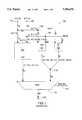
- FIG. 1is a block diagram illustrating a conventional multiplier circuit 100 which performs one 18-bit multiplication or two 9-bit multiplications.
- Multiplier circuit 100includes input ports 101 and 102, 18-bit multiplier 110, 9-bit multipliers 120 and 121, multiplexer 130 and output port 103.
- Eighteen-bit words A[17:0] and B[17:0]are provided to multiplier circuit 100 at input ports 101 and 102, respectively.
- Eighteen-bit word A[17:0]consists of a 9-bit upper byte A[17:9] and a 9-bit lower byte A[8:0].
- 18-bit word B[17:0]consists of a 9-bit upper byte B[17:9] and a 9-bit lower byte B[8:0].
- 18-bit words A[17:0] and B[17:0]are provided to 18-bit multiplier 110.
- 18-bit multiplier 110is a conventional device which contains at least four 9-bit multipliers similar to 9-bit multipliers 120 and 121.
- the output signal of 18-bit multiplier 110is a 36-bit (in parallel) word output signal which is equal to the product of A[17:0] and B[17:0].
- a multiplexer select signal on lead 131causes multiplexer 130 to route the 36 output bits of 18-bit multiplier 110 to output port 103.
- Multiplier circuit 100is also capable of performing two 9-bit multiplications. To do this, 9-bit upper byte A[17:9] is multiplied by 9-bit upper byte B[17:9] to form a first 18-bit product and 9-bit lower byte A[18:0] is multiplied by 9-bit lower byte B[8:0] to form a second 18-bit product. Thus, 18-bit word A[17:0] is separated into two 9-bit bytes A[17:9] and A[8:0] at port 150.
- Nine-bit byte A[17:9]is provided to an input bus of multiplier 120 and 9-bit byte A[8:0] is provided to an input bus of multiplier 121.
- 18-bit word B[17:0]is separated into two 9-bit bytes B[17:9] and B[8:0] at port 151.
- Nine-bit byte B[17:9]is provided to an input bus of multiplier 120 and 9-bit byte B[8:0] is provided to an input bus of multiplier circuit 121.
- Nine-bit multiplier 120is a conventional multiplier circuit which produces an 18-bit word equal to A[17:9]*B[17:9].
- Nine-bit multiplier 121is typically identical to 9-bit multiplier 120.
- the output signal of 9-bit multiplier 121is equal to A[8:0]*B[8:0].
- the output signals of multipliers 120 and 121are concatenated at port 152, resulting in a 36-bit output signal.
- the upper half of this 36-bit output signalis equal to the product of A[17:9] and B[17:9] and the lower half of this 36-bit output signal is equal to the product of A[8:0] and B[8:0]. Consequently, the two 9-bit multiplications previously described have been performed.
- a multiplexer select signal on lead 131causes multiplexer 130 to route the 36-bit output signal of concatenation port 152 to output port 103.
- multiplier circuit 100requires an 18-bit multiplier 110, two 9-bit multipliers 120 and 121, and multiplexer 130, the area required to fabricate multiplier circuit 100 is significant. Because of the desire to minimize the layout area of integrated circuits, it would be advantageous to have a multiplier circuit with a reduced area which is capable of selectably performing either a large multiplication or two small multiplications.
- first and second wordsare provided to respective first and second input ports of a multiplier circuit. Both words have an upper byte and a lower byte.
- the multiplier circuitcan be selected to multiply the first and second words in a first mode.
- the multiplier circuitcan also be selected to multiply the upper bytes of the first and second words and the lower bytes of the first and second words in a second mode.
- the multiplier circuithas four multipliers. In the first mode, all four multipliers are used to multiply the first and second words. In the second mode, two of the four multipliers are effectively disabled by a multiplier select signal and the remaining two multipliers are used to multiply the upper bytes of the first and second words and the lower bytes of the first and second words.
- a first multiplieris coupled to the first and second input ports in such a manner as to receive the upper bytes of the first and second words.
- the first multiplier circuitgenerates a first product equal to the product of these upper bytes.
- a second multiplieris coupled to the first and second input ports in such a manner as to receive the lower bytes of the first and second words.
- the second multiplier circuitgenerates a second product equal to the product of these lower bytes.
- a third multiplieris coupled to the second input port and the first gating circuit in such a manner as to receive the lower byte of the second word and the output signal of a first gating circuit.
- the third multiplier circuitgenerates a third product equal to the product of the lower byte of the second word and the output signal of the first gating circuit.
- a fourth multiplieris coupled to the second input port and a second gating circuit in such a manner as to receive the upper byte of the second word and the output signal of the second gating circuit.
- the fourth multiplier circuitgenerates a fourth product equal to the product of the upper byte of the second word and the output signal of the second gating circuit.
- the first gating circuitis coupled to the first input port in such a manner as to receive the upper byte of the first word and the multiplier select signal.
- the second gating circuitis coupled to the first input port in such a manner to receive the lower byte of the first word and the multiplier select signal.
- the multiplier select signaldetermines whether the first and second gating circuits pass the upper and lower bytes of the first word, respectively, or zero values.
- the multiplier select signalWhen the multiplier select signal is in a first state, the first mode of the multiplier circuit is selected and the first and second gating circuits pass the upper and lower bytes of the first word, respectively.
- the multiplier select signalWhen the multiplier select signal is in a second state, the second mode of the multiplier circuit is selected and the output signals of the first and second gating circuits are zero.
- Another embodiment of the present inventionincludes a method of selectably multiplying a first word having an upper byte and a lower byte and a second word having an upper byte and a lower byte.
- the upper byte of the first wordis multiplied with the upper byte of the second word to create a first product.
- the lower byte of the first wordis multiplied with the lower byte of the second word to create a second product.
- the first and second productsare then concatenated to form a first concatenated word.
- the lower byte of the first wordis multiplied with a selectable signal to create a first byte and the upper byte of the first word is multiplied with the selectable signal to create a second byte.
- the first byteis multiplied with the upper byte of the second word to create a third product and the second byte is multiplied with the lower byte of the second word to create a fourth product.
- the third and fourth productsare then added to create a first sum.
- the selectable signalis selected to be one to perform the multiplication of the two words.
- the selectable signalis selected to be zero to perform the multiplication of the upper bytes of the first and second words and the multiplication of the lower bytes of the first and second words.
- FIG. 1is a block diagram of a prior art multiplier circuit
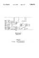
- FIG. 2is a block diagram of a multiplier circuit in accordance with one embodiment of the present invention.
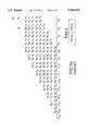
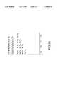
- FIG. 3which consists of FIGS. 3a and 3b, is a schematic diagram illustrating longhand multiplication of two 9-bit numbers to obtain an 18-bit product
- FIG. 4is a schematic diagram of a conventional 9-bit Wallace tree adder (FIG. 4 consists of FIGS. 4A-1, 4A-2 and 4b);
- FIG. 5ais a schematic diagram of a carry save adder
- FIG. 5bis a truth table for the carry save adder of FIG. 5a.
- FIG. 6is a schematic diagram of a gating circuit in accordance with one embodiment of the present invention.
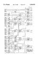
- FIG. 2is a block diagram of multiplier circuit 200 in accordance with one embodiment of the present invention. Although the present invention is described in connection with circuitry which performs either an 18-bit multiplication or two 9-bit multiplications, the present invention is easily modified to perform multiplications with other numbers of bits.
- 18-bit product A[8:0]*B[8:0]contributes to the value of the lower 18-bits C[17:0] of the resultant 36-bit product (i.e., product A[8:0]*B[8:0] is multiplied by 2 0 ).
- the 18-bit product A[17:9]*B[17:9]contributes to the value of the upper 18-bits C[35:18] of the resultant 36-bit product (i.e., product A[17:9]*B[17:9] is multiplied by 2 18 ).
- Multiplier circuit 200performs the above-described 18-bit multiplication as follows. Eighteen-bit word A[17:0] is provided to input port 201 and is divided into two 9-bit bytes A[17:9] and A[8:0] at port 206. Nine-bit upper byte A[17:9] is provided to an input bus of gating circuit 240 and to an input bus of 9-bit multiplier 232. Nine-bit lower byte A[8:0] is provided to an input bus of gating circuit 241 and an input bus of 9-bit multiplier 231. In one embodiment, 9-bit multipliers 230 and 231 utilize conventional Wallace tree adders.
- FIG. 4is a schematic diagram of a conventional 9-bit Wallace tree adder 400 which can be used to multiply 9-bit numbers X[8:0] and Y[8:0].
- FIG. 4consists of FIGS. 4a-1, 4a-2 and 4b. Leads 471-475 couple FIGS. 4a and 4b as illustrated.
- Carry save adders 401-461 of Wallace tree adder 400are used to create sum bits S[17:0] and carry bits C[17:0].
- FIG. 5ais a schematic diagram of carry save adder 401 and FIG. 5b is a truth table for carry save adder 401.
- Carry save adders 402-461are identical to carry save adder 401.
- a 1-bit multiplier select signalis provided at port 204.
- This multiplier select signalis typically generated in response to a system operation code and is routed to input leads of gating circuits 240 and 241. As described in more detail later, the multiplier select signal determines whether multiplier circuit 200 operates as an 18-bit multiplier or two 9-bit multipliers.
- the output signals of gating circuits 240 and 241are provided to input buses of 9-bit multipliers 230 and 233, respectively.
- An 18-bit word B[17:0]is provided to input port 202.
- Eighteen-bit word B[17:0]is separated into 9-bit upper byte B[17:9] and 9-bit lower byte B[8:0] at port 208.
- Lower byte B[8:0]is provided to input buses of 9-bit multipliers 230 and 231 and upper byte B[17:9] is provided to input buses of 9-bit multipliers 232 and 233.
- 9-bit multipliers 232 and 233are identical to 9-bit multipliers 230 and 231.
- the output signals of multipliers 231 and 232are provided to concatenation port 244.
- the output signal of concatenation port 244is provided to summing circuit 235.
- the output signals of multipliers 230 and 233are provided to summing circuit 234.
- the output signal of summing circuit 234is transmitted through concatenation port 245 to summing circuit 235.
- the output signal of summing circuit 235is provided to output port 203.
- Multiplier circuit 200operates as follows. To perform an 18-bit multiply, the multiplier select signal at input port 204 is set to a logic high level, thereby providing a high signal to gating circuit 240.
- FIG. 6is a schematic diagram of one embodiment of gating circuit 240.
- the multiplier select signalis provided to an input lead of each of AND gates 301-309. Each bit of byte A[17:9] is applied to an input lead of one of AND gates 301-309. Gating circuit 240 thereby performs a logical AND operation on each of the bits in upper byte A[17:9].
- the high input signal from input port 204causes upper byte A[17:9] to be transmitted through gating circuit 240 to an input bus of multiplier 230.
- gating circuit 240is described in connection with a single embodiment, it is understood that other gating circuits can be substituted for gating circuit 240 without departing from the scope of the present invention.
- gating circuit 241is formed in the same manner as gating circuit 240.
- the high input signal at input port 204causes lower byte A[8:0] to be transmitted through gating circuit 241 to an input bus of multiplier 233.
- the output signal of multiplier 230is an 18-bit product equal to A[17:9]*B[8:0]
- the output signal of multiplier 231is an 18-bit product equal to A[8:0]*B[8:0]
- the output signal of multiplier 232is an 18-bit product equal to A[17:9]*B[17:9]
- the output signal of multiplier 233is an 18-bit product equal to A[8:0]*B[17:9].
- the output signals of multipliers 231 and 232are concatenated at port 244 to produce a 36-bit output signal.
- the upper 18-bits of this output signalare equal to the 18-bit product A[17:9]*B[17:9] and the lower 18-bits of this output signal are equal to the 18-bit product A[8:0]*B[8:0].
- the output signal of concatenation port 244is therefore equal to:
- the output signals of multipliers 230 and 233are added in summing circuit 234.
- the output signal of summing circuit 234is equal to:
- the output signal of summing circuit 234has 19-bits to include any carry bit required by the addition of the two 18-bit input words.
- the 19-bit output signal of summing circuit 234is provided to concatenation port 245 where 8 "zero" bits are added at the beginning of the 19-bit output signal and 9 "zero" bits are added after the 19-bit output signal of summing circuit port 234.
- the 36-bit output signal of concatenation port 245is therefore equal to:
- the 36-bit output signal of concatenation port 245is provided to summing circuit 235.
- Summing circuit 235adds the output signals of concatenation ports 244 and 245 to produce a 36-bit output signal at output port 203 which is equal to:
- the multiplication select signal at port 204is set to a logic low state. This causes the 9-bit output signals of gating circuits 240 and 241 to be zero. Consequently, the output signals of multipliers 230 and 233 are zero. As a result, the output signals of summing circuit 234 and concatenation port 245 are also zero. Multipliers 231 and 232 operate as previously discussed in connection with the 18-bit multiplication. Thus, the upper 18-bits of the 36-bit output signal of concatenation port 244 are equal to the 18-bit product of 9-bit upper bytes A[17:9] and B[17:9].
- the lower 18-bits of the 36-bit output signal of concatenation port 244are equal to the 18-bit product of 9-bit lower bytes A[8:0] and B[8:0].
- the 36-bit output signal of concatenation port 244is passed through summing circuit 235 to output port 203 unchanged because the other input signal provided to summing circuit 235 (from concatenation port 245) is zero.
- Multiplier circuit 200thereby selectably performs either an 18-bit multiplication or two 9-bit multiplications.
- multiplier circuit 200When compared with multiplier circuit 100 (FIG. 1), multiplier circuit 200 eliminates the need for 9-bit multipliers 120 and 121 and multiplexer 130. Thus, multiplier circuit can be fabricated with a smaller layout area than prior art multiplier circuits.
Landscapes
- Physics & Mathematics (AREA)
- General Physics & Mathematics (AREA)
- Computational Mathematics (AREA)
- Mathematical Analysis (AREA)
- Mathematical Optimization (AREA)
- Pure & Applied Mathematics (AREA)
- Engineering & Computer Science (AREA)
- Theoretical Computer Science (AREA)
- Computing Systems (AREA)
- General Engineering & Computer Science (AREA)
- Complex Calculations (AREA)
Abstract
Description
A[17:9]*B[17:9]*2.sup.18 +A[8:0]*B[8:0]*2.sup.0.
A[17:9]*B[8:0]+A[8:0]*B[17:9].
(A[17:9]*B[8:0]+A[8:0]*B[17:9]) * 2.sup.9.
A[17:9]*B[17:9]*2.sup.18 +(A[17:9]*B[8:0]+A[8:0]*B[17:9])*2.sup.9 +A[8:0]*B[8:0]*2.sup.0
Claims (11)
Priority Applications (1)
| Application Number | Priority Date | Filing Date | Title |
|---|---|---|---|
| US08/285,376US5586070A (en) | 1994-08-03 | 1994-08-03 | Structure and method for embedding two small multipliers in a larger multiplier |
Applications Claiming Priority (1)
| Application Number | Priority Date | Filing Date | Title |
|---|---|---|---|
| US08/285,376US5586070A (en) | 1994-08-03 | 1994-08-03 | Structure and method for embedding two small multipliers in a larger multiplier |
Publications (1)
| Publication Number | Publication Date |
|---|---|
| US5586070Atrue US5586070A (en) | 1996-12-17 |
Family
ID=23093974
Family Applications (1)
| Application Number | Title | Priority Date | Filing Date |
|---|---|---|---|
| US08/285,376Expired - LifetimeUS5586070A (en) | 1994-08-03 | 1994-08-03 | Structure and method for embedding two small multipliers in a larger multiplier |
Country Status (1)
| Country | Link |
|---|---|
| US (1) | US5586070A (en) |
Cited By (25)
| Publication number | Priority date | Publication date | Assignee | Title |
|---|---|---|---|---|
| US5742538A (en)* | 1993-11-30 | 1998-04-21 | Texas Instruments Incorporated | Long instruction word controlling plural independent processor operations |
| US5999959A (en)* | 1998-02-18 | 1999-12-07 | Quantum Corporation | Galois field multiplier |
| US6014684A (en)* | 1997-03-24 | 2000-01-11 | Intel Corporation | Method and apparatus for performing N bit by 2*N-1 bit signed multiplication |
| US6199090B1 (en) | 1998-06-19 | 2001-03-06 | Ati International Srl | Double incrementing, low overhead, adder |
| US20010037352A1 (en)* | 1998-11-04 | 2001-11-01 | Hong John Suk-Hyun | Multiplier capable of multiplication of large multiplicands and parallel multiplications small multiplicands |
| US6418529B1 (en) | 1998-03-31 | 2002-07-09 | Intel Corporation | Apparatus and method for performing intra-add operation |
| US6460064B1 (en) | 1998-11-02 | 2002-10-01 | Hyundai Electronics Industries Co. Ltd. | Multiplier for operating n bits and n/2 bits and method therefor |
| US6523055B1 (en) | 1999-01-20 | 2003-02-18 | Lsi Logic Corporation | Circuit and method for multiplying and accumulating the sum of two products in a single cycle |
| US6704762B1 (en)* | 1998-08-28 | 2004-03-09 | Nec Corporation | Multiplier and arithmetic unit for calculating sum of product |
| US20040059889A1 (en)* | 1998-03-31 | 2004-03-25 | Macy William W. | Method and apparatus for performing efficient transformations with horizontal addition and subtraction |
| US20040153632A1 (en)* | 1995-08-16 | 2004-08-05 | Microunity Systems Engineering, Inc. | Method and software for partitioned group element selection operation |
| US20050102344A1 (en)* | 2003-11-06 | 2005-05-12 | Telefonaktiebolaget Lm Ericsson (Pub1) | Split radix multiplication |
| US7062526B1 (en)* | 2000-02-18 | 2006-06-13 | Texas Instruments Incorporated | Microprocessor with rounding multiply instructions |
| US7395302B2 (en) | 1998-03-31 | 2008-07-01 | Intel Corporation | Method and apparatus for performing horizontal addition and subtraction |
| US20080195685A1 (en)* | 2007-01-10 | 2008-08-14 | Analog Devices, Inc. | Multi-format multiplier unit |
| US7506017B1 (en)* | 2004-05-25 | 2009-03-17 | Altera Corporation | Verifiable multimode multipliers |
| US20090094309A1 (en)* | 1995-08-16 | 2009-04-09 | Microunity Systems Engineering, Inc. | System and method to implement a matrix multiply unit of a broadband processor |
| US20150081753A1 (en)* | 2013-09-13 | 2015-03-19 | Nvidia Corporation | Technique for performing arbitrary width integer arithmetic operations using fixed width elements |
| US9069624B1 (en)* | 2012-07-23 | 2015-06-30 | Altera Corporation | Systems and methods for DSP block enhancement |
| US9606608B1 (en)* | 2014-03-19 | 2017-03-28 | Altera Corporation | Low power optimizations for a floating point multiplier |
| US20190042198A1 (en)* | 2018-09-27 | 2019-02-07 | Intel Corporation | Methods for using a multiplier to support multiple sub-multiplication operations |
| CN111176609A (en)* | 2018-11-12 | 2020-05-19 | 三星电子株式会社 | Multiplier and method of operation |
| CN111596886A (en)* | 2019-02-21 | 2020-08-28 | 超威半导体公司 | Hybrid matrix multiplication pipeline |
| US10776078B1 (en)* | 2018-09-23 | 2020-09-15 | Groq, Inc. | Multimodal multiplier systems and methods |
| US11262980B2 (en)* | 2018-01-09 | 2022-03-01 | Samsung Electronics Co., Ltd. | Computing accelerator using a lookup table |
Citations (9)
| Publication number | Priority date | Publication date | Assignee | Title |
|---|---|---|---|---|
| JPS5769451A (en)* | 1980-10-17 | 1982-04-28 | Toshiba Corp | Lsi multiplication block |
| US4594679A (en)* | 1983-07-21 | 1986-06-10 | International Business Machines Corporation | High speed hardware multiplier for fixed floating point operands |
| US4754421A (en)* | 1985-09-06 | 1988-06-28 | Texas Instruments Incorporated | Multiple precision multiplication device |
| US4809212A (en)* | 1985-06-19 | 1989-02-28 | Advanced Micro Devices, Inc. | High throughput extended-precision multiplier |
| US4811269A (en)* | 1985-10-09 | 1989-03-07 | Hitachi, Ltd. | Bit slice multiplication circuit |
| US4825401A (en)* | 1986-03-31 | 1989-04-25 | Kabushiki Kaisha Toshiba | Functional dividable multiplier array circuit for multiplication of full words or simultaneous multiplication of two half words |
| US4868778A (en)* | 1987-05-19 | 1989-09-19 | Harris Corporation | Speed enhancement for multipliers using minimal path algorithm |
| US4989168A (en)* | 1987-11-30 | 1991-01-29 | Fujitsu Limited | Multiplying unit in a computer system, capable of population counting |
| US5138574A (en)* | 1986-09-17 | 1992-08-11 | Fujitsu Limited | Method and device for obtaining sum of products using integrated circuit |
- 1994
- 1994-08-03USUS08/285,376patent/US5586070A/ennot_activeExpired - Lifetime
Patent Citations (9)
| Publication number | Priority date | Publication date | Assignee | Title |
|---|---|---|---|---|
| JPS5769451A (en)* | 1980-10-17 | 1982-04-28 | Toshiba Corp | Lsi multiplication block |
| US4594679A (en)* | 1983-07-21 | 1986-06-10 | International Business Machines Corporation | High speed hardware multiplier for fixed floating point operands |
| US4809212A (en)* | 1985-06-19 | 1989-02-28 | Advanced Micro Devices, Inc. | High throughput extended-precision multiplier |
| US4754421A (en)* | 1985-09-06 | 1988-06-28 | Texas Instruments Incorporated | Multiple precision multiplication device |
| US4811269A (en)* | 1985-10-09 | 1989-03-07 | Hitachi, Ltd. | Bit slice multiplication circuit |
| US4825401A (en)* | 1986-03-31 | 1989-04-25 | Kabushiki Kaisha Toshiba | Functional dividable multiplier array circuit for multiplication of full words or simultaneous multiplication of two half words |
| US5138574A (en)* | 1986-09-17 | 1992-08-11 | Fujitsu Limited | Method and device for obtaining sum of products using integrated circuit |
| US4868778A (en)* | 1987-05-19 | 1989-09-19 | Harris Corporation | Speed enhancement for multipliers using minimal path algorithm |
| US4989168A (en)* | 1987-11-30 | 1991-01-29 | Fujitsu Limited | Multiplying unit in a computer system, capable of population counting |
Cited By (52)
| Publication number | Priority date | Publication date | Assignee | Title |
|---|---|---|---|---|
| USRE44190E1 (en)* | 1993-11-30 | 2013-04-30 | Texas Instruments Incorporated | Long instruction word controlling plural independent processor operations |
| US7389317B2 (en)* | 1993-11-30 | 2008-06-17 | Texas Instruments Incorporated | Long instruction word controlling plural independent processor operations |
| US5742538A (en)* | 1993-11-30 | 1998-04-21 | Texas Instruments Incorporated | Long instruction word controlling plural independent processor operations |
| US20080077771A1 (en)* | 1993-11-30 | 2008-03-27 | Guttag Karl M | Long Instruction Word Controlling Plural Independent Processor Operations |
| US20030105793A1 (en)* | 1993-11-30 | 2003-06-05 | Guttag Karl M. | Long instruction word controlling plural independent processor operations |
| US8769248B2 (en) | 1995-08-16 | 2014-07-01 | Microunity Systems Engineering, Inc. | System and apparatus for group floating-point inflate and deflate operations |
| US8195735B2 (en)* | 1995-08-16 | 2012-06-05 | Microunity Systems Engineering, Inc. | System and method to implement a matrix multiply unit of a broadband processor |
| US8117426B2 (en) | 1995-08-16 | 2012-02-14 | Microunity Systems Engineering, Inc | System and apparatus for group floating-point arithmetic operations |
| US8001360B2 (en) | 1995-08-16 | 2011-08-16 | Microunity Systems Engineering, Inc. | Method and software for partitioned group element selection operation |
| US8683182B2 (en) | 1995-08-16 | 2014-03-25 | Microunity Systems Engineering, Inc. | System and apparatus for group floating-point inflate and deflate operations |
| US20090094309A1 (en)* | 1995-08-16 | 2009-04-09 | Microunity Systems Engineering, Inc. | System and method to implement a matrix multiply unit of a broadband processor |
| US20040153632A1 (en)* | 1995-08-16 | 2004-08-05 | Microunity Systems Engineering, Inc. | Method and software for partitioned group element selection operation |
| US6370559B1 (en)* | 1997-03-24 | 2002-04-09 | Intel Corportion | Method and apparatus for performing N bit by 2*N−1 bit signed multiplications |
| US6014684A (en)* | 1997-03-24 | 2000-01-11 | Intel Corporation | Method and apparatus for performing N bit by 2*N-1 bit signed multiplication |
| US5999959A (en)* | 1998-02-18 | 1999-12-07 | Quantum Corporation | Galois field multiplier |
| US20040059889A1 (en)* | 1998-03-31 | 2004-03-25 | Macy William W. | Method and apparatus for performing efficient transformations with horizontal addition and subtraction |
| US7395302B2 (en) | 1998-03-31 | 2008-07-01 | Intel Corporation | Method and apparatus for performing horizontal addition and subtraction |
| US6418529B1 (en) | 1998-03-31 | 2002-07-09 | Intel Corporation | Apparatus and method for performing intra-add operation |
| US20030050941A1 (en)* | 1998-03-31 | 2003-03-13 | Patrice Roussel | Apparatus and method for performing intra-add operation |
| US6961845B2 (en) | 1998-03-31 | 2005-11-01 | Intel Corporation | System to perform horizontal additions |
| US7392275B2 (en) | 1998-03-31 | 2008-06-24 | Intel Corporation | Method and apparatus for performing efficient transformations with horizontal addition and subtraction |
| US6199090B1 (en) | 1998-06-19 | 2001-03-06 | Ati International Srl | Double incrementing, low overhead, adder |
| US6704762B1 (en)* | 1998-08-28 | 2004-03-09 | Nec Corporation | Multiplier and arithmetic unit for calculating sum of product |
| US6460064B1 (en) | 1998-11-02 | 2002-10-01 | Hyundai Electronics Industries Co. Ltd. | Multiplier for operating n bits and n/2 bits and method therefor |
| US6915322B2 (en)* | 1998-11-04 | 2005-07-05 | Dsp Group, Inc. | Multiplier capable of multiplication of large multiplicands and parallel multiplications of small multiplicands |
| US20010037352A1 (en)* | 1998-11-04 | 2001-11-01 | Hong John Suk-Hyun | Multiplier capable of multiplication of large multiplicands and parallel multiplications small multiplicands |
| US6523055B1 (en) | 1999-01-20 | 2003-02-18 | Lsi Logic Corporation | Circuit and method for multiplying and accumulating the sum of two products in a single cycle |
| US7062526B1 (en)* | 2000-02-18 | 2006-06-13 | Texas Instruments Incorporated | Microprocessor with rounding multiply instructions |
| US8943119B2 (en) | 2001-09-04 | 2015-01-27 | Microunity Systems Engineering, Inc. | System and method to implement a matrix multiply unit of a broadband processor |
| US20050102344A1 (en)* | 2003-11-06 | 2005-05-12 | Telefonaktiebolaget Lm Ericsson (Pub1) | Split radix multiplication |
| US7318080B2 (en)* | 2003-11-06 | 2008-01-08 | Telefonaktiebolaget L M Ericsson (Publ) | Split radix multiplication |
| US8095899B1 (en) | 2004-05-25 | 2012-01-10 | Altera Corporation | Verifiable multimode multipliers |
| US7506017B1 (en)* | 2004-05-25 | 2009-03-17 | Altera Corporation | Verifiable multimode multipliers |
| US8336007B1 (en) | 2004-05-25 | 2012-12-18 | Altera Corporation | Verifiable multimode multipliers |
| US20080195685A1 (en)* | 2007-01-10 | 2008-08-14 | Analog Devices, Inc. | Multi-format multiplier unit |
| US8275822B2 (en)* | 2007-01-10 | 2012-09-25 | Analog Devices, Inc. | Multi-format multiplier unit |
| US9069624B1 (en)* | 2012-07-23 | 2015-06-30 | Altera Corporation | Systems and methods for DSP block enhancement |
| US20150081753A1 (en)* | 2013-09-13 | 2015-03-19 | Nvidia Corporation | Technique for performing arbitrary width integer arithmetic operations using fixed width elements |
| US9600235B2 (en)* | 2013-09-13 | 2017-03-21 | Nvidia Corporation | Technique for performing arbitrary width integer arithmetic operations using fixed width elements |
| US9606608B1 (en)* | 2014-03-19 | 2017-03-28 | Altera Corporation | Low power optimizations for a floating point multiplier |
| US11262980B2 (en)* | 2018-01-09 | 2022-03-01 | Samsung Electronics Co., Ltd. | Computing accelerator using a lookup table |
| US11042360B1 (en) | 2018-09-23 | 2021-06-22 | Groq, Inc. | Multiplier circuitry for multiplying operands of multiple data types |
| US10776078B1 (en)* | 2018-09-23 | 2020-09-15 | Groq, Inc. | Multimodal multiplier systems and methods |
| US10871946B2 (en)* | 2018-09-27 | 2020-12-22 | Intel Corporation | Methods for using a multiplier to support multiple sub-multiplication operations |
| US20190042198A1 (en)* | 2018-09-27 | 2019-02-07 | Intel Corporation | Methods for using a multiplier to support multiple sub-multiplication operations |
| US10963220B2 (en)* | 2018-11-12 | 2021-03-30 | Samsung Electronics Co., Ltd. | Signed multiplication using unsigned multiplier with dynamic fine-grained operand isolation |
| CN111176609A (en)* | 2018-11-12 | 2020-05-19 | 三星电子株式会社 | Multiplier and method of operation |
| US11579842B2 (en) | 2018-11-12 | 2023-02-14 | Samsung Electronics Co., Ltd. | Signed multiplication using unsigned multiplier with dynamic fine-grained operand isolation |
| TWI801690B (en)* | 2018-11-12 | 2023-05-11 | 南韓商三星電子股份有限公司 | Multiplier and method to multiply first operand and second operand |
| US11775256B2 (en) | 2018-11-12 | 2023-10-03 | Samsung Electronics Co., Ltd. | Signed multiplication using unsigned multiplier with dynamic fine-grained operand isolation |
| CN111596886A (en)* | 2019-02-21 | 2020-08-28 | 超威半导体公司 | Hybrid matrix multiplication pipeline |
| US11347827B2 (en)* | 2019-02-21 | 2022-05-31 | Advanced Micro Devices, Inc. | Hybrid matrix multiplication pipeline |
Similar Documents
| Publication | Publication Date | Title |
|---|---|---|
| US5586070A (en) | Structure and method for embedding two small multipliers in a larger multiplier | |
| US5771186A (en) | System and method for multiplying in a data processing system | |
| US4153938A (en) | High speed combinatorial digital multiplier | |
| US5751622A (en) | Structure and method for signed multiplication using large multiplier having two embedded signed multipliers | |
| US5327369A (en) | Digital adder and method for adding 64-bit, 16-bit and 8-bit words | |
| US6055555A (en) | Interface for performing parallel arithmetic and round operations | |
| US6066960A (en) | Programmable logic device having combinational logic at inputs to logic elements within logic array blocks | |
| US6286023B1 (en) | Partitioned adder tree supported by a multiplexer configuration | |
| US4751663A (en) | IIR digital filter | |
| US4130878A (en) | Expandable 4 × 8 array multiplier | |
| US5943251A (en) | Adder which handles multiple data with different data types | |
| US5343417A (en) | Fast multiplier | |
| US4346451A (en) | Dual moduli exponent transform type high speed multiplication system | |
| US6065033A (en) | Wallace-tree multipliers using half and full adders | |
| US5646877A (en) | High radix multiplier architecture | |
| JP3556950B2 (en) | Structure and method for reducing the number of carry look-ahead adder stages in high speed arithmetic devices | |
| US6260056B1 (en) | Circuit and method for fast squaring by breaking the square into a plurality of terms | |
| US4319335A (en) | Arithmetic logic unit controller | |
| US5586071A (en) | Enhanced fast multiplier | |
| US5357457A (en) | Adder with carry look ahead circuit | |
| US5477479A (en) | Multiplying system having multi-stages for processing a digital signal based on the Booth's algorithm | |
| US6460064B1 (en) | Multiplier for operating n bits and n/2 bits and method therefor | |
| US5623434A (en) | Structure and method of using an arithmetic and logic unit for carry propagation stage of a multiplier | |
| US5719802A (en) | Adder circuit incorporating byte boundaries | |
| KR0147942B1 (en) | Booth recording circuit in multiplier |
Legal Events
| Date | Code | Title | Description |
|---|---|---|---|
| AS | Assignment | Owner name:XENON MICROSYSTEMS, INC., CALIFORNIA Free format text:ASSIGNMENT OF ASSIGNORS INTEREST;ASSIGNOR:PURCELL, STEPHEN C.;REEL/FRAME:007104/0833 Effective date:19940803 | |
| AS | Assignment | Owner name:CHROMATIC RESEARCH, INC., CALIFORNIA Free format text:CHANGE OF NAME;ASSIGNOR:XENON MICROSYSTEMS CORPORATION;REEL/FRAME:007853/0422 Effective date:19941123 | |
| STCF | Information on status: patent grant | Free format text:PATENTED CASE | |
| AS | Assignment | Owner name:SILICON VALLEY BANK, CALIFORNIA Free format text:SECURITY INTEREST;ASSIGNOR:CHROMATIC RESEARCH, INC.;REEL/FRAME:009375/0853 Effective date:19980409 | |
| AS | Assignment | Owner name:SILICON VALLEY BANK, CALIFORNIA Free format text:RELEASE;ASSIGNOR:CHROMATIC RESEARCH, INC.;REEL/FRAME:009773/0725 Effective date:19990218 | |
| AS | Assignment | Owner name:ATI RESEARCH SILICON VALLEY INC., CALIFORNIA Free format text:CHANGE OF NAME;ASSIGNOR:CHROMATIC RESEARCH, INC.;REEL/FRAME:010226/0012 Effective date:19990129 | |
| AS | Assignment | Owner name:ATI TECHNOLOGIES INC., CANADA Free format text:ASSIGNMENT OF ASSIGNORS INTEREST;ASSIGNOR:ATI RESEARCH SILICON VALLEY INC.;REEL/FRAME:010206/0952 Effective date:19990811 | |
| AS | Assignment | Owner name:ATI INTERNATIONAL SRL, BARBADOS Free format text:ASSIGNMENT OF ASSIGNORS INTEREST;ASSIGNOR:ATI TECHNOLOGIES, INC.;REEL/FRAME:010226/0984 Effective date:19990813 | |
| FPAY | Fee payment | Year of fee payment:4 | |
| FPAY | Fee payment | Year of fee payment:8 | |
| FPAY | Fee payment | Year of fee payment:12 | |
| AS | Assignment | Owner name:ATI TECHNOLOGIES ULC, CANADA Free format text:ASSIGNMENT OF ASSIGNORS INTEREST;ASSIGNOR:ATI INTERNATIONAL SRL;REEL/FRAME:023574/0593 Effective date:20091118 Owner name:ATI TECHNOLOGIES ULC,CANADA Free format text:ASSIGNMENT OF ASSIGNORS INTEREST;ASSIGNOR:ATI INTERNATIONAL SRL;REEL/FRAME:023574/0593 Effective date:20091118 |