US5585695A - Thin film electroluminescent display module - Google Patents
Thin film electroluminescent display moduleDownload PDFInfo
- Publication number
- US5585695A US5585695AUS08/464,006US46400695AUS5585695AUS 5585695 AUS5585695 AUS 5585695AUS 46400695 AUS46400695 AUS 46400695AUS 5585695 AUS5585695 AUS 5585695A
- Authority
- US
- United States
- Prior art keywords
- display
- light permeable
- display module
- counterelectrode
- electroluminescent
- Prior art date
- Legal status (The legal status is an assumption and is not a legal conclusion. Google has not performed a legal analysis and makes no representation as to the accuracy of the status listed.)
- Expired - Fee Related
Links
- 239000010409thin filmSubstances0.000titleabstractdescription13
- 239000000758substrateSubstances0.000claimsabstractdescription58
- 230000004888barrier functionEffects0.000claimsdescription8
- 239000000463materialSubstances0.000claimsdescription6
- 238000000576coating methodMethods0.000claimsdescription5
- 239000011248coating agentSubstances0.000claimsdescription4
- 230000001681protective effectEffects0.000claimsdescription2
- 239000012212insulatorSubstances0.000abstractdescription16
- 238000007789sealingMethods0.000abstractdescription12
- 238000003491arrayMethods0.000abstractdescription3
- 239000004020conductorSubstances0.000abstractdescription2
- 238000004519manufacturing processMethods0.000abstractdescription2
- 239000011159matrix materialSubstances0.000abstractdescription2
- 229910052751metalInorganic materials0.000description17
- 239000002184metalSubstances0.000description17
- 239000011521glassSubstances0.000description15
- 238000000151depositionMethods0.000description7
- 238000005530etchingMethods0.000description7
- 239000010408filmSubstances0.000description7
- 230000000873masking effectEffects0.000description7
- 230000008021depositionEffects0.000description6
- XAGFODPZIPBFFR-UHFFFAOYSA-NaluminiumChemical compound[Al]XAGFODPZIPBFFR-UHFFFAOYSA-N0.000description5
- 239000004033plasticSubstances0.000description5
- 229920003023plasticPolymers0.000description5
- 229910007277Si3 N4Inorganic materials0.000description4
- XLOMVQKBTHCTTD-UHFFFAOYSA-NZinc monoxideChemical compound[Zn]=OXLOMVQKBTHCTTD-UHFFFAOYSA-N0.000description4
- 238000000034methodMethods0.000description4
- 230000003287optical effectEffects0.000description4
- 229910052581Si3N4Inorganic materials0.000description3
- VYPSYNLAJGMNEJ-UHFFFAOYSA-NSilicium dioxideChemical compoundO=[Si]=OVYPSYNLAJGMNEJ-UHFFFAOYSA-N0.000description3
- 229910052782aluminiumInorganic materials0.000description3
- 230000008878couplingEffects0.000description3
- 238000010168coupling processMethods0.000description3
- 238000005859coupling reactionMethods0.000description3
- 238000005516engineering processMethods0.000description3
- HQVNEWCFYHHQES-UHFFFAOYSA-Nsilicon nitrideChemical compoundN12[Si]34N5[Si]62N3[Si]51N64HQVNEWCFYHHQES-UHFFFAOYSA-N0.000description3
- 229910000679solderInorganic materials0.000description3
- 239000004593EpoxySubstances0.000description2
- XUIMIQQOPSSXEZ-UHFFFAOYSA-NSiliconChemical compound[Si]XUIMIQQOPSSXEZ-UHFFFAOYSA-N0.000description2
- 230000007423decreaseEffects0.000description2
- 239000004973liquid crystal related substanceSubstances0.000description2
- 229910052710siliconInorganic materials0.000description2
- 239000010703siliconSubstances0.000description2
- 229910052814silicon oxideInorganic materials0.000description2
- 238000004544sputter depositionMethods0.000description2
- 239000011787zinc oxideSubstances0.000description2
- RYGMFSIKBFXOCR-UHFFFAOYSA-NCopperChemical compound[Cu]RYGMFSIKBFXOCR-UHFFFAOYSA-N0.000description1
- VVQNEPGJFQJSBK-UHFFFAOYSA-NMethyl methacrylateChemical compoundCOC(=O)C(C)=CVVQNEPGJFQJSBK-UHFFFAOYSA-N0.000description1
- OAICVXFJPJFONN-UHFFFAOYSA-NPhosphorusChemical compound[P]OAICVXFJPJFONN-UHFFFAOYSA-N0.000description1
- 229920005372Plexiglas®Polymers0.000description1
- 239000004642PolyimideSubstances0.000description1
- 230000004913activationEffects0.000description1
- CSDREXVUYHZDNP-UHFFFAOYSA-NalumanylidynesiliconChemical compound[Al].[Si]CSDREXVUYHZDNP-UHFFFAOYSA-N0.000description1
- 230000008901benefitEffects0.000description1
- 230000015556catabolic processEffects0.000description1
- 239000004568cementSubstances0.000description1
- 238000005234chemical depositionMethods0.000description1
- 229910052802copperInorganic materials0.000description1
- 239000010949copperSubstances0.000description1
- 230000003247decreasing effectEffects0.000description1
- 239000003989dielectric materialSubstances0.000description1
- 238000005401electroluminescenceMethods0.000description1
- 229920006333epoxy cementPolymers0.000description1
- 230000006872improvementEffects0.000description1
- 229910003437indium oxideInorganic materials0.000description1
- PJXISJQVUVHSOJ-UHFFFAOYSA-Nindium(iii) oxideChemical compound[O-2].[O-2].[O-2].[In+3].[In+3]PJXISJQVUVHSOJ-UHFFFAOYSA-N0.000description1
- AMGQUBHHOARCQH-UHFFFAOYSA-Nindium;oxotinChemical compound[In].[Sn]=OAMGQUBHHOARCQH-UHFFFAOYSA-N0.000description1
- 229910052909inorganic silicateInorganic materials0.000description1
- 239000011810insulating materialSubstances0.000description1
- 238000007737ion beam depositionMethods0.000description1
- 239000007788liquidSubstances0.000description1
- 229910044991metal oxideInorganic materials0.000description1
- 150000004706metal oxidesChemical class0.000description1
- TWNQGVIAIRXVLR-UHFFFAOYSA-Noxo(oxoalumanyloxy)alumaneChemical compoundO=[Al]O[Al]=OTWNQGVIAIRXVLR-UHFFFAOYSA-N0.000description1
- SIWVEOZUMHYXCS-UHFFFAOYSA-Noxo(oxoyttriooxy)yttriumChemical compoundO=[Y]O[Y]=OSIWVEOZUMHYXCS-UHFFFAOYSA-N0.000description1
- BPUBBGLMJRNUCC-UHFFFAOYSA-Noxygen(2-);tantalum(5+)Chemical compound[O-2].[O-2].[O-2].[O-2].[O-2].[Ta+5].[Ta+5]BPUBBGLMJRNUCC-UHFFFAOYSA-N0.000description1
- 230000002093peripheral effectEffects0.000description1
- 238000005289physical depositionMethods0.000description1
- 229920001721polyimidePolymers0.000description1
- 229920000642polymerPolymers0.000description1
- 239000000843powderSubstances0.000description1
- 230000008569processEffects0.000description1
- 230000005855radiationEffects0.000description1
- 238000012552reviewMethods0.000description1
- 229910002027silica gelInorganic materials0.000description1
- 239000000741silica gelSubstances0.000description1
- 229920002545silicone oilPolymers0.000description1
- 229910052709silverInorganic materials0.000description1
- 239000004332silverSubstances0.000description1
- 239000007787solidSubstances0.000description1
- 230000003068static effectEffects0.000description1
- 229910001936tantalum oxideInorganic materials0.000description1
- 238000002207thermal evaporationMethods0.000description1
- XOLBLPGZBRYERU-UHFFFAOYSA-Ntin dioxideChemical compoundO=[Sn]=OXOLBLPGZBRYERU-UHFFFAOYSA-N0.000description1
- 229910001887tin oxideInorganic materials0.000description1
Images


Classifications
- H—ELECTRICITY
- H05—ELECTRIC TECHNIQUES NOT OTHERWISE PROVIDED FOR
- H05B—ELECTRIC HEATING; ELECTRIC LIGHT SOURCES NOT OTHERWISE PROVIDED FOR; CIRCUIT ARRANGEMENTS FOR ELECTRIC LIGHT SOURCES, IN GENERAL
- H05B33/00—Electroluminescent light sources
- H05B33/02—Details
- H05B33/04—Sealing arrangements, e.g. against humidity
- H—ELECTRICITY
- H05—ELECTRIC TECHNIQUES NOT OTHERWISE PROVIDED FOR
- H05B—ELECTRIC HEATING; ELECTRIC LIGHT SOURCES NOT OTHERWISE PROVIDED FOR; CIRCUIT ARRANGEMENTS FOR ELECTRIC LIGHT SOURCES, IN GENERAL
- H05B33/00—Electroluminescent light sources
- H05B33/02—Details
- H05B33/06—Electrode terminals
- H—ELECTRICITY
- H05—ELECTRIC TECHNIQUES NOT OTHERWISE PROVIDED FOR
- H05B—ELECTRIC HEATING; ELECTRIC LIGHT SOURCES NOT OTHERWISE PROVIDED FOR; CIRCUIT ARRANGEMENTS FOR ELECTRIC LIGHT SOURCES, IN GENERAL
- H05B33/00—Electroluminescent light sources
- H05B33/12—Light sources with substantially two-dimensional radiating surfaces
- H05B33/26—Light sources with substantially two-dimensional radiating surfaces characterised by the composition or arrangement of the conductive material used as an electrode
Definitions
- This inventionrelates to thin film electroluminescent (EL) display modules which may be tiled together to form a larger EL display panel.
- ELelectroluminescent
- ELelectroluminescent
- a tiled displayrequires individual display tiles or modules that may be placed in close proximity to give the appearance of a continuous display.
- plasmaliquid crystal
- vacuum fluorescenceEL
- the latterhas the advantage that connections may, in principle, be placed anywhere on the module. This is possible because the device consists of one glass sheet with a series of solid state coatings.
- Liquid crystal, vacuum fluorescent and plasma modulesrequire both front and rear sealing (usually glass) that restricts the connection paths to the module edges.
- a sealis required to prevent gas or liquid leakage at the edges of the module. The combination of seals and electrical connections makes it extremely difficult to tile modules especially at higher pixel resolutions.
- U.S. Pat. No. 5,124,204 issued to Yamashita et al.briefly reviews a typical prior art EL panel comprising the display elements formed on a glass substrate.
- This prior art EL panelis sealed by a glass cover sheet bonded to the glass substrate with silicone oil, containing silica gel powder, being sealed between the display element and the cover sheet.
- This arrangementis both heavy and results in a significant gap between the edge of the glass substrate and the outer edge of the display element.
- Yamashita et al.reduces the weight problem by replacing the glass cover sheet with a polymer based moisture-proof sheet; however, the drawback of the edge gaps remains thereby precluding tiling together of multiple modules.
- U.S. Pat. No. 4,266,223 issued to Framediscloses a display device comprising thin film transistor circuits for sequentially switching a brightness control signal to an array of individual display elements.
- the devicecomprises transversely-spaced or interdigitated metallic electrode finger arrays deposited onto a glass substrate and an electroluminescent layer deposited on top thereof which is then coated with an insulator and then contact electrodes. Transistor arrays are then deposited on top of these display elements. Transversely-spaced electrodes and thin film transistor circuits are difficult and expensive to manufacture.
- an electroluminescent display modulecomprising an EL layer structure which avoids the need for edge connections and edge sealing so that the active area of each module extends to the edge of that module such that no extra gap is visible between active areas of adjacent modules tiled together. It would also be advantageous in such a structure to use a transparent substrate with an EL structure that allows connections to the rear of the substrate whereby the light reaches the viewer through the transparent substrate from the front.
- the present inventionfeatures an outer light permeable or transparent substrate (e.g., plastic or glass) upon which is added a series of conducting, insulating and radiating thin films which comprise a third film EL structure.
- the layers comprising the EL structureare patterned to create openings and/or separated regions in various layers, such as to define a number of display elements and connection pads for electrical activation of the EL display elements.
- the present inventionalso provides a means of sealing the moisture sensitive thin film layer or layers from ambient conditions.
- the present inventionalso provides an EL electronic driver chip that is mounted above the EL display elements on the back side of the substrate and connected with the EL connection pads.
- the EL driver chipis able to control the intensity of the radiation emitted from the display elements.
- an electroluminescent display modulecomprising a light permeable substrate having a front, a back and side edges.
- the moduleincludes an array of display elements comprising a light permeable electrically conductive base coated on said substrate, CL plurality of electroluminescent areas, and a counterelectrode coating at least part of each electroluminescent area.
- One of either the light permeable electrically conductive base or the counterelectrodeis patterned to provide a plurality of electrically isolated sections each with an associated exposed contact pad, and the other of the conductive base and counterelectrode is a common electrode to at least some of the electroluminescent areas.
- Each electroluminescent areais sandwiched between an electrically isolated section and the common electrode.
- the contact padsare spaced inwardly from the substrate edges so that electrical contact to the array of display elements is made to the display module spaced away from the edges of the substrate.
- a plurality of the EL display modulescan be tiled together in edge-to-edge relationship to form an electroluminescent display panel.
- an electroluminescent display modulecomprising a plurality of light permeable substrates having a front, back and side edges.
- the plurality of light permeable substratesare tiled together in edge-to-edge relationship to form an expandable display panel.
- the moduleincludes an array of display elements spaced on the back side of the light permeable substrate each comprising a light permeable electrically conductive base portion coated on the light permeable substrate, a counterelectrode and an electroluminescent material sandwiched between the conductive base portion and a portion of the counterelectrode.
- the moduleincludes a display driver chip with a plurality of contact pins mounted on the substrate.
- the display driver chipis mounted on the back side of the light permeable substrate with each pin being electrically connected to a preselected number of display elements at positions spaced inwardly from the substrate edges. Control signal means is attached to the counterelectrode.
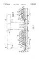
- FIG. 1is a cross sectional view, broken away, of a layered EL display structure of an EL module constructed in accordance with the present invention
- FIG. 2shows a pattern for the conductive ITO electrode layer deposited onto a glass substrate for a 35 element EL display module shown in cross section in FIG. 1;
- FIG. 3is a top view of the pattern formed by the electroluminescent layer sandwiched by two insulator layers in the display element of FIG. 1;
- FIG. 4is a top view of the pattern formed by a conducting metal layer deposited onto the sandwich structure shown in FIG. 3;
- FIG. 5is a top view of the pattern formed by a sealing layer deposited onto the metal layer and sandwich array of FIGS. 3 and 4;
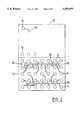
- FIG. 6shows part of a signal control circuit and driver chip with protruding connectors to be electrically connected to the EL display of FIG. 1;
- FIG. 7is a cross sectional view of an alternative embodiment of a display element similar to FIG. 1 showing the EL layer sandwiched completely by two insulating layers;
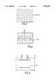
- FIG. 8is a cross sectional view, broken away, of an alternative embodiment of an EL module containing 256 display elements
- FIG. 9is a top view of the pattern of a conducting ITO base of the EL module of FIG. 8;
- FIG. 10is a top view of the pattern formed when a first insulating layer is deposited onto the ITO pattern of FIG. 9;
- FIG. 11is a top view of the pattern formed by the generally superimposed electroluminescence layer sandwiched by two insulator layers in the display element of FIG. 8;
- FIG. 12is a top view of the pattern formed by the conducting metal layer deposited onto the sandwich structure shown in FIG. 11;
- FIG. 13is cross sectional view of another embodiment of the EL display device including a lens attached to the viewing side of the display substrate.
- FIG. 1a cross section of essentially one and a half display elements or pixels of an electroluminescent (EL) module constructed in accordance with the present invention is shown.
- a display element 10is formed on a standard 1.1 mm thick light permeable substrate 12 upon which a transparent or generally light permeable and electrically conductive thin (500-3000 ⁇ ) coating 13 is deposited.
- Substrate 12may be glass or plastic but other suitable substrates may also be used depending on the application.
- a preferred conductive coatingis one of several conducting metal oxides, preferably indium-tin-oxide (ITO), tin oxide, indium oxide or aluminum doped zinc oxide (ZnO:Al).
- ITOindium-tin-oxide
- tin oxideindium oxide or aluminum doped zinc oxide (ZnO:Al).
- ZnO:Alaluminum doped zinc oxide
- the conducting oxidemay be deposited by any of a number of physical or chemical deposition processes such as atomic sputtering, ion beam deposition and thermal evaporation to mention just a few.
- FIG. 2An example of a final pattern of the deposited ITO layer 13 is shown in FIG. 2 and comprises an array of 35 (5 ⁇ 7) circular ITO electrodes 14 each interconnected to an associated connector pad 28 which is exposed in the assembled module.
- This patternmay be obtained by using suitable masks during deposition of the ITO, or alternatively, the ITO may be deposited as a continuous layer and then etched afterward to provide the pattern of FIG. 2 using known masking/etching procedures.
- a transparent thin (1000-5000 ⁇ ) insulator layer 16is then deposited on top of the conducting oxide and patterned using similar masking or etching techniques used to deposit the conductive oxide layer 13.
- Insulator layer 16is a thin film dielectric insulating material such as silicon oxy-nitride, silicon-aluminum oxy-nitride, tantalum oxide, aluminum oxide, yttrium oxide or other known thin film dielectric material having high breakdown strength.
- FIGS. 3 to 5show the mask patterns used in conjunction with the ITO patterned layer 13 of FIG. 2 and will be more fully discussed below.
- a thin (4,000-10,000 ⁇ ) electroluminescent layer 18(which functions essentially as a phosphor layer) is then deposited onto the patterned conductive oxide layer portion 14 coated by insulator layer 16 leaving portion 28 exposed.
- a preferred electroluminescent materialis such as ZnS:Mn but other materials which could be used include SrS:Ce, Zn 2 SiO 4 :Mn or ZnS:TbF.
- EL layer 18is patterned either by masking during growth or by etching after growth similar to the other two layers.
- Another transparent thin dielectric or insulator layer 20is deposited to cover EL layer 18 and may be the same material comprising layer 16 with a comparable thickness.
- An electrically conductive thin film ( ⁇ 2000 ⁇ ) counterelectrode layer 22 of for example aluminumis deposited and patterned either by masking during growth or by etching after growth.
- a sealing layer 24is then deposited and in a preferred embodiment layer 24 is silicon nitride Si 3 N 4 applied by sputtering.
- the Si 3 N 4 layeris patterned by either masking during deposition or etching thereafter to produce the patterned layer 18 of FIG. 1 wherein the aluminum metal film 22 is exposed at 26 to provide an electrical contact pad to aluminum layer 22 common to all pixels while patterned conducting oxide layer 13 is exposed at 28 to provide an electrical contact pad to each pixel 10.
- the ITO electrode base 13comprises a first portion 14 which underlies each display element 10 and a second exposed portion 28 to which electrical contact is made to form the control circuit to drive the display elements.
- FIG. 3is a top view of the pattern formed by the generally superimposed layers 16, 18 and the top insulating layer 20 deposited on the larger ITO contacts 14 of FIG. 2 to form the display elements or pixels 10.
- Each display element 10is provided with an associated smaller ITO contact pad 28 shown in FIGS. 1 and 2.
- FIG. 4shows the top view of the pattern formed in conductive layer 22 showing contact pad 26.
- Metal layer 22at least partially covers the sandwich structure (14/16/18/20) in FIG. 1 and each contact pad 26 is connected with a drive signal to be described below.
- FIG. 5shows the top view of the pattern formed by the silicon nitride (Si 3 N 4 ) sealing layer 24.
- the 35 electrical pads 28 in FIG. 2are shown exposed through sealing layer 24 which are contacted by contacts 30 projecting from driver chips 32 which are mounted directly above the sealing layer 24 (FIG. 6) which will now be discussed.
- a typical EL driver chip 32is a silicon integrated circuit, for example Supertax Inc, HV577, which is sealed in a plastic package and mounted on a printed circuit board (PCB) with 35 contacts 30 projecting therefrom each to contact a contact pad 28. Adhesion and good electrical contact between contacts 30 and contact pads 28 may be achieved using, for example, conductive pastes, conductive epoxy or solder. If solder is used then contact pads 28 are preferably coated with a suitable metal such as copper or silver before the solder is applied. Contact pad 26 is connected to a wire 34 using conductive paste or conductive epoxy. Wire 34 is connected to an AC drive signal of 150 V. By supplying suitable voltage control signals to ITO pads 14 through driver chips 32 connected to ITO pads 28, control of the associated display elements or pixels is achieved.
- PCBprinted circuit board
- a thin glass plate or plastic cover sheetmay be used with apertures etched or drilled through the plate or sheet to form the pattern shown in FIG. 5. This protective cover is bonded to the back of the layered EL structure using epoxy cement.
- FIG. 7illustrates a portion of an alternative embodiment of a 5 ⁇ 7 display module at 40 which is very similar to the EL display module of FIG. 1.
- the ITO pattern 13is the same as shown in FIG. 2 but in the cross section in FIG. 7 the EL layer 18 is sealed between the dielectric insulating layers 16 and 20 which both extend beyond the EL layer.
- the purpose of insulating layers 16 and 20are to insulate EL layer 18 from ITO contacts 14 and metal layer 22 so that any configuration which accomplishes this would be suitable.
- Display modulessuch as illustrated in FIGS. 1 and 7 with the 5 ⁇ 7 array achieved over 100 fL brightness with circular pixels.
- FIG. 2shows two substrates 12 (one in ghost outline) tiled together wherein the gap between the display elements on the edges of adjacent substrates is the same as the gap between the display elements on the same substrate.
- a conductive ITO pattern 44is first deposited onto substrate 12, best seen in FIG. 9 comprising circular ITO pads 14 and rectangular contact pads 28. The pattern as shown is obtained either during deposition or by etching afterwards.
- a thin film insulating layer 52is deposited, see FIG. 10. Insulating layer 52 is preferably silicon oxide (SiO 2 ) or polyimide and is deposited to a thickness in the range 0.5 to 3 ⁇ m. Insulator layer 16, EL layer 18, and insulator layer 20 are then sequentially deposited using appropriate masking during deposition or etching after deposition.
- Metal film 22is then deposited with suitable masking to provide four separate metallized areas each having one contact pad 54 (best seen in FIG. 12) to provide a plurality of display elements 50.
- Display elements 50lack the silicon nitride Si 3 N 4 sealing layer 24 used in display elements shown in FIG. 1.
- insulator layer 20acts as a moisture barrier or seal in place of layer 24.
- the presence of insulating layer 52allows metal layer 22 to pass directly above portions of conductive ITO film 14 which in this embodiment are common to four pixels and contact pads 54 may also be placed above layer 14.
- insulator layer 52allows portions of ITO film 44 to pass below metal film 22 where desired.
- Each display element 50is connected to the driver chips (not shown) and control signal source through the chip connections being made to ITO pads 28 and contact pads 54 on metal layer 22 on top of insulator layer 52 respectively.
- This geometryis advantageous if complex arrangements of light emitting elements and electrical contact pads are to be realized, since it allows layers 14 and 22 to pass under or over each other.
- the top view of the pattern of the conducting ITO layer of the embodiment shown in FIG. 8includes 256 circular ITO areas 14 wherein each ITO circle is connected to three other ITO circles. Electrical contact to each set of four connected ITO circles 14 is through the small rectangular ITO contact pad 28 (of which there are 64). Each ITO contact pad 28 is connected to one of 64 drivers contained in a driver chip (not shown).
- the top view in FIG. 10shows the pattern formed by insulator layer 52 with the three white strips indicating the exposed contact pads 28.
- FIG. 11is a top view of the pattern formed by the generally superimposed layers 16, 18 and 20 of FIG. 8. FIG.
- FIG. 12shows the top view of the pattern formed by conductive film 22 deposited onto layer 20 wherein insulator layer 20 is exposed along the three generally rectangular perimeters. This results in four metallic regions insulated from each other formed in layer 22. Each region is connected to a wire at a metal contact pad 54. Each ITO contact pad 28 is connected to one of 64 drivers contained in a driver chip (not shown) which is adhered to the module by bonding each of 64 pin connectors to the 64 ITO contact pads 28.
- Operation of the display module of FIGS. 8 to 12utilizes multiplexing to address display elements 50.
- an AC drive signalis applied via a first one of the four metallic contacts 54 to layer 22 of FIG. 12 connecting a driver (not shown) to the first region of metal layer 22.
- the 64 drivers connected to the display elements via the contact pads 28 in FIG. 9supply AC signals that either add to, or subtract from, the voltage applied to the first region of metal layer 22 which turns on, or off, respectively, the corresponding 64 display elements that are covered by the first driven region of layer 22 of FIG. 12.
- a second of the four contact pads 54is driven in place of the first, and the 64 drivers connected to the display elements are driven so as to turn on or off the corresponding 64 display elements that are covered by this second metal region of metal layer 22.
- the third and then the fourth contact pad 54 in FIG. 12is driven in appropriate synchronization with drivers driving the display elements via contact pads 28 so as to turn on or off the remainder of the 256 display elements.
- the entire aforementioned sequencethen repeats itself at a rate of about 100 times per second to give the appearance of a static display in which each display element may be on or off.
- plastic lenses 90were bonded to the viewing side of substrate 12 to improve light collection from the pixels.
- Light that is normally internally reflected in the glassmay be coupled out effectively using a plano-convex lens.
- Plexiglasswas machined into lenses 90 that were bonded to the front of substrate 12 using optical cement.
- the use of lenses 90increased the optical area of the pixels by up to 4 times without decreasing pixel brightness. This represents a four-fold improvement in optical coupling at a normal viewing angle, which is in line with estimated coupling efficiencies of 8-20% without lenses.
- the use of lensesalso decreases or almost eliminates the apparent gaps between the display elements or pixels which makes the spacing of pixels in these modules useful for conductor paths which are not apparent to the viewer. However, the use of lenses decreases the viewing angle in that adjacent lenses block light from one another. A viewing angle of ⁇ 50° is typical with lenses.
- the EL layer 18may also be effectively sealed if dielectric layers 16 and 20 extend beyond the EL layer as shown in FIG. 7 where the dielectric layers essentially envelop EL layer 18. Thus, EL layer 18 may be broken into separate regions for each display element or pixel, while dielectric layers 16 and 20 are continuous between display elements.
- the display modules using thin film EL technology constructed in accordance with the present inventionare advantageous over the prior art EL devices because they permit pixel displays to be constructed wherein the electrical connection to the layers on the light permeable transparent substrate can be made away from the edges of each substrate thereby minimizing tile gaps.
- Driver chipsmay be mounted with or without PCB's directly onto the back side of substrate 12 above the EL pixels opposite to the side which is viewed.
- the array of electroluminescent display elements in the modules shown in FIGS. 1, 7 and 8can extend across the full length of substrate 12 from edge-to-edge. A multiple number of the EL modules may then be tiled together in edge-to-edge relation to form a larger EL display panel.
- the Use of patterned circular pixelsallows simple hemispherical lenses to be mounted directly onto the viewing side of the transparent substrate to enhance optical coupling, and insulator layer 52 advantageously permits electrode crossovers in more complex layouts.
- the EL modules constructed according to the present inventionmatched brightness levels of commercially available light emitting diode (LED) modules using less power so that the low cost integrated thin film EL technology utilized in the present invention is a viable alternative to standard LED configurations.
- LEDlight emitting diode
- each row and column patterncould be patterned on one EL module and contact pads to each row and each column pattern could be fabricated.
- the display elementsneed not be arranged in a rectangular array but rather in a circle or any other desired manner to suit the application at hand.
- Each pixelcan be of any shape, circular, rectangular or any other shape depending on the application at hand in accordance with the patterns chosen for layers 14, 16, 18, 20, 22 and layer 52 if present.
- Layer 52may be used to define complex pixel shapes such as letters, symbols, or even a pixel comprising a group of non-continuous light emitting elements.
- the conducting layers 14 and 18may be continuous and the boundaries of the shape of light element or elements forming the pixel may be determined solely by the geometry of layer 52.
- electroluminescent display modulehas been described and illustrated with respect to the embodiments disclosed herein, it will be appreciated by those skilled in the art that numerous variations of these embodiments may be made without departing from the scope of the invention described herein.
Landscapes
- Electroluminescent Light Sources (AREA)
- Devices For Indicating Variable Information By Combining Individual Elements (AREA)
Abstract
Description
This invention relates to thin film electroluminescent (EL) display modules which may be tiled together to form a larger EL display panel.
It is desirable to have an economical means of producing electroluminescent (EL) display modules that can be tiled together. A tiled display requires individual display tiles or modules that may be placed in close proximity to give the appearance of a continuous display. Of the four major flat panel technologies: plasma, liquid crystal, vacuum fluorescence and EL, the latter has the advantage that connections may, in principle, be placed anywhere on the module. This is possible because the device consists of one glass sheet with a series of solid state coatings. Liquid crystal, vacuum fluorescent and plasma modules require both front and rear sealing (usually glass) that restricts the connection paths to the module edges. In addition, a seal is required to prevent gas or liquid leakage at the edges of the module. The combination of seals and electrical connections makes it extremely difficult to tile modules especially at higher pixel resolutions.
Currently, X-Y matrix addressing is employed for EL displays and connections are made at the edges of the glass such as disclosed in U.S. Pat. No. 4,999,539 issued to Coovert et al. The surface area occupied by these connectors uses space near the peripheral edges of the module thereby producing a large gap between the display area and the edge of the substrate. Another drawback of conventional EL display modules is that many employ moisture barriers covering the entire back of the module for preventing moisture or other undesired ambient elements from entering the layered EL structure which are sealed around the perimeter of the glass substrate. These moisture barriers also result in a gap between the display area and the edge of the substrate. Thus, areas around the edge of the module used for connections and sealing do not allow for radiating display elements to exist in these areas. This causes the module dimensions to exceed the active area of the module which adds to module size, weight and cost.
U.S. Pat. No. 5,124,204 issued to Yamashita et al. briefly reviews a typical prior art EL panel comprising the display elements formed on a glass substrate. This prior art EL panel is sealed by a glass cover sheet bonded to the glass substrate with silicone oil, containing silica gel powder, being sealed between the display element and the cover sheet. This arrangement is both heavy and results in a significant gap between the edge of the glass substrate and the outer edge of the display element. Yamashita et al. reduces the weight problem by replacing the glass cover sheet with a polymer based moisture-proof sheet; however, the drawback of the edge gaps remains thereby precluding tiling together of multiple modules.
U.S. Pat. No. 4,266,223 issued to Frame discloses a display device comprising thin film transistor circuits for sequentially switching a brightness control signal to an array of individual display elements. The device comprises transversely-spaced or interdigitated metallic electrode finger arrays deposited onto a glass substrate and an electroluminescent layer deposited on top thereof which is then coated with an insulator and then contact electrodes. Transistor arrays are then deposited on top of these display elements. Transversely-spaced electrodes and thin film transistor circuits are difficult and expensive to manufacture.
It would therefore be advantageous to provide an electroluminescent display module comprising an EL layer structure which avoids the need for edge connections and edge sealing so that the active area of each module extends to the edge of that module such that no extra gap is visible between active areas of adjacent modules tiled together. It would also be advantageous in such a structure to use a transparent substrate with an EL structure that allows connections to the rear of the substrate whereby the light reaches the viewer through the transparent substrate from the front.
It is an object of the present invention to provide an EL module comprising a multitude of radiating display elements which may be electrically controlled with driver circuitry mounted directly on the rear of the module thereby reducing the number of external connections necessary to operate the module.
It is another object of the present invention to provide an EL module which significantly reduces the gap between the light emitting display elements and the edge of the substrate thereby facilitating tiling of multiple EL modules.
The present invention features an outer light permeable or transparent substrate (e.g., plastic or glass) upon which is added a series of conducting, insulating and radiating thin films which comprise a third film EL structure. The layers comprising the EL structure are patterned to create openings and/or separated regions in various layers, such as to define a number of display elements and connection pads for electrical activation of the EL display elements.
The present invention also provides a means of sealing the moisture sensitive thin film layer or layers from ambient conditions. The present invention also provides an EL electronic driver chip that is mounted above the EL display elements on the back side of the substrate and connected with the EL connection pads. The EL driver chip is able to control the intensity of the radiation emitted from the display elements.
In one aspect of the present invention there is provided an electroluminescent display module comprising a light permeable substrate having a front, a back and side edges. The module includes an array of display elements comprising a light permeable electrically conductive base coated on said substrate, CL plurality of electroluminescent areas, and a counterelectrode coating at least part of each electroluminescent area. One of either the light permeable electrically conductive base or the counterelectrode is patterned to provide a plurality of electrically isolated sections each with an associated exposed contact pad, and the other of the conductive base and counterelectrode is a common electrode to at least some of the electroluminescent areas. Each electroluminescent area is sandwiched between an electrically isolated section and the common electrode. The contact pads are spaced inwardly from the substrate edges so that electrical contact to the array of display elements is made to the display module spaced away from the edges of the substrate.
A plurality of the EL display modules can be tiled together in edge-to-edge relationship to form an electroluminescent display panel.
In another aspect of the invention there is provided an electroluminescent display module comprising a plurality of light permeable substrates having a front, back and side edges. The plurality of light permeable substrates are tiled together in edge-to-edge relationship to form an expandable display panel. The module includes an array of display elements spaced on the back side of the light permeable substrate each comprising a light permeable electrically conductive base portion coated on the light permeable substrate, a counterelectrode and an electroluminescent material sandwiched between the conductive base portion and a portion of the counterelectrode. The module includes a display driver chip with a plurality of contact pins mounted on the substrate. The display driver chip is mounted on the back side of the light permeable substrate with each pin being electrically connected to a preselected number of display elements at positions spaced inwardly from the substrate edges. Control signal means is attached to the counterelectrode.
The electroluminescent (EL) module constructed in accordance with the present invention will now be described, by way of example only, reference being had to the accompanying drawings, in which:
FIG. 1 is a cross sectional view, broken away, of a layered EL display structure of an EL module constructed in accordance with the present invention;
FIG. 2 shows a pattern for the conductive ITO electrode layer deposited onto a glass substrate for a 35 element EL display module shown in cross section in FIG. 1;
FIG. 3 is a top view of the pattern formed by the electroluminescent layer sandwiched by two insulator layers in the display element of FIG. 1;
FIG. 4 is a top view of the pattern formed by a conducting metal layer deposited onto the sandwich structure shown in FIG. 3;
FIG. 5 is a top view of the pattern formed by a sealing layer deposited onto the metal layer and sandwich array of FIGS. 3 and 4;
FIG. 6 shows part of a signal control circuit and driver chip with protruding connectors to be electrically connected to the EL display of FIG. 1;
FIG. 7 is a cross sectional view of an alternative embodiment of a display element similar to FIG. 1 showing the EL layer sandwiched completely by two insulating layers;
FIG. 8 is a cross sectional view, broken away, of an alternative embodiment of an EL module containing 256 display elements;
FIG. 9 is a top view of the pattern of a conducting ITO base of the EL module of FIG. 8;
FIG. 10 is a top view of the pattern formed when a first insulating layer is deposited onto the ITO pattern of FIG. 9;
FIG. 11 is a top view of the pattern formed by the generally superimposed electroluminescence layer sandwiched by two insulator layers in the display element of FIG. 8;
FIG. 12 is a top view of the pattern formed by the conducting metal layer deposited onto the sandwich structure shown in FIG. 11; and
FIG. 13 is cross sectional view of another embodiment of the EL display device including a lens attached to the viewing side of the display substrate.
In the ensuing description of the structure and operation of the EL display devices constructed in accordance with the present invention, like numerals in the drawings of different embodiments refer to the same materials. Referring first to FIG. 1, a cross section of essentially one and a half display elements or pixels of an electroluminescent (EL) module constructed in accordance with the present invention is shown. Adisplay element 10 is formed on a standard 1.1 mm thick lightpermeable substrate 12 upon which a transparent or generally light permeable and electrically conductive thin (500-3000 Å) coating 13 is deposited.Substrate 12 may be glass or plastic but other suitable substrates may also be used depending on the application. A preferred conductive coating is one of several conducting metal oxides, preferably indium-tin-oxide (ITO), tin oxide, indium oxide or aluminum doped zinc oxide (ZnO:Al). The conducting oxide may be deposited by any of a number of physical or chemical deposition processes such as atomic sputtering, ion beam deposition and thermal evaporation to mention just a few.
An example of a final pattern of the depositedITO layer 13 is shown in FIG. 2 and comprises an array of 35 (5×7)circular ITO electrodes 14 each interconnected to an associatedconnector pad 28 which is exposed in the assembled module. This pattern may be obtained by using suitable masks during deposition of the ITO, or alternatively, the ITO may be deposited as a continuous layer and then etched afterward to provide the pattern of FIG. 2 using known masking/etching procedures. After deposition of the patterned conducting oxide layer 13 a transparent thin (1000-5000 Å)insulator layer 16 is then deposited on top of the conducting oxide and patterned using similar masking or etching techniques used to deposit theconductive oxide layer 13.Insulator layer 16 is a thin film dielectric insulating material such as silicon oxy-nitride, silicon-aluminum oxy-nitride, tantalum oxide, aluminum oxide, yttrium oxide or other known thin film dielectric material having high breakdown strength. FIGS. 3 to 5 show the mask patterns used in conjunction with the ITO patternedlayer 13 of FIG. 2 and will be more fully discussed below.
A thin (4,000-10,000 Å) electroluminescent layer 18 (which functions essentially as a phosphor layer) is then deposited onto the patterned conductiveoxide layer portion 14 coated byinsulator layer 16 leavingportion 28 exposed. A preferred electroluminescent material is such as ZnS:Mn but other materials which could be used include SrS:Ce, Zn2 SiO4 :Mn or ZnS:TbF.EL layer 18 is patterned either by masking during growth or by etching after growth similar to the other two layers. Another transparent thin dielectric orinsulator layer 20 is deposited to coverEL layer 18 and may be the samematerial comprising layer 16 with a comparable thickness.
An electrically conductive thin film (˜2000 Å)counterelectrode layer 22 of for example aluminum is deposited and patterned either by masking during growth or by etching after growth. Asealing layer 24 is then deposited and in apreferred embodiment layer 24 is silicon nitride Si3 N4 applied by sputtering. The Si3 N4 layer is patterned by either masking during deposition or etching thereafter to produce the patternedlayer 18 of FIG. 1 wherein thealuminum metal film 22 is exposed at 26 to provide an electrical contact pad toaluminum layer 22 common to all pixels while patterned conductingoxide layer 13 is exposed at 28 to provide an electrical contact pad to eachpixel 10. Thus, theITO electrode base 13 comprises afirst portion 14 which underlies eachdisplay element 10 and a second exposedportion 28 to which electrical contact is made to form the control circuit to drive the display elements.
FIG. 3 is a top view of the pattern formed by the generally superimposedlayers layer 20 deposited on thelarger ITO contacts 14 of FIG. 2 to form the display elements orpixels 10. Eachdisplay element 10 is provided with an associated smallerITO contact pad 28 shown in FIGS. 1 and 2. FIG. 4 shows the top view of the pattern formed inconductive layer 22showing contact pad 26.Metal layer 22 at least partially covers the sandwich structure (14/16/18/20) in FIG. 1 and eachcontact pad 26 is connected with a drive signal to be described below. FIG. 5 shows the top view of the pattern formed by the silicon nitride (Si3 N4) sealinglayer 24. The 35electrical pads 28 in FIG. 2 are shown exposed through sealinglayer 24 which are contacted bycontacts 30 projecting fromdriver chips 32 which are mounted directly above the sealing layer 24 (FIG. 6) which will now be discussed.
Referring specifically to FIG. 6, a typicalEL driver chip 32 is a silicon integrated circuit, for example Supertax Inc, HV577, which is sealed in a plastic package and mounted on a printed circuit board (PCB) with 35contacts 30 projecting therefrom each to contact acontact pad 28. Adhesion and good electrical contact betweencontacts 30 andcontact pads 28 may be achieved using, for example, conductive pastes, conductive epoxy or solder. If solder is used then contactpads 28 are preferably coated with a suitable metal such as copper or silver before the solder is applied.Contact pad 26 is connected to awire 34 using conductive paste or conductive epoxy.Wire 34 is connected to an AC drive signal of 150 V. By supplying suitable voltage control signals toITO pads 14 throughdriver chips 32 connected toITO pads 28, control of the associated display elements or pixels is achieved.
Whenaluminum metal layer 22 is connected to a dive signal by awire 34 connected to contactpad 26, it is driven by an AC drive signal that is set to a voltage of 150 V peak or below the turn-on voltage of the EL display elements. When an additional AC voltage is applied to a particular EL display pixel viacontact pad 28 by means ofdriver chip 32 such that it's voltage of 50 V adds to the voltage onmetal layer 22 then the corresponding EL pixel turns on sustaining a voltage of 200 V peak AC and light is emitted from that particular pixel. If theconductive portion 14 of the ITO base forming part of eachpixel 10 is driven such that the applied voltage subtracts from the voltage applied tometal layer 22, then it turns off. In this way the array of display elements may be controlled individually.
Other methods of sealing the display modules instead of depositing a thin insulating layer may be utilized. Specifically, a thin glass plate or plastic cover sheet may be used with apertures etched or drilled through the plate or sheet to form the pattern shown in FIG. 5. This protective cover is bonded to the back of the layered EL structure using epoxy cement.
FIG. 7 illustrates a portion of an alternative embodiment of a 5×7 display module at 40 which is very similar to the EL display module of FIG. 1. TheITO pattern 13 is the same as shown in FIG. 2 but in the cross section in FIG. 7 theEL layer 18 is sealed between the dielectric insulatinglayers layers EL layer 18 fromITO contacts 14 andmetal layer 22 so that any configuration which accomplishes this would be suitable. Display modules such as illustrated in FIGS. 1 and 7 with the 5×7 array achieved over 100 fL brightness with circular pixels. BecauseITO contact pads 28 andcontact pad 26 are spaced inwardly from the edges ofsubstrate 12, multiple display elements can be tiled together in edge-to-edge relationship. FIG. 2 shows two substrates 12 (one in ghost outline) tiled together wherein the gap between the display elements on the edges of adjacent substrates is the same as the gap between the display elements on the same substrate.
Referring to FIGS. 8 to 12, an alternative embodiment of an EL display module is shown. A conductive ITO pattern 44 is first deposited ontosubstrate 12, best seen in FIG. 9 comprisingcircular ITO pads 14 andrectangular contact pads 28. The pattern as shown is obtained either during deposition or by etching afterwards. Upon completion of pattern 44, a thinfilm insulating layer 52 is deposited, see FIG. 10. Insulatinglayer 52 is preferably silicon oxide (SiO2) or polyimide and is deposited to a thickness in the range 0.5 to 3 μm.Insulator layer 16,EL layer 18, andinsulator layer 20 are then sequentially deposited using appropriate masking during deposition or etching after deposition.Metal film 22 is then deposited with suitable masking to provide four separate metallized areas each having one contact pad 54 (best seen in FIG. 12) to provide a plurality ofdisplay elements 50.Display elements 50 lack the silicon nitride Si3 N4 sealing layer 24 used in display elements shown in FIG. 1. In the embodiment shown in FIGS. 8 to 12,insulator layer 20 acts as a moisture barrier or seal in place oflayer 24. The presence of insulatinglayer 52 allowsmetal layer 22 to pass directly above portions ofconductive ITO film 14 which in this embodiment are common to four pixels andcontact pads 54 may also be placed abovelayer 14. Thus,insulator layer 52 allows portions of ITO film 44 to pass belowmetal film 22 where desired. Eachdisplay element 50 is connected to the driver chips (not shown) and control signal source through the chip connections being made toITO pads 28 andcontact pads 54 onmetal layer 22 on top ofinsulator layer 52 respectively. This geometry is advantageous if complex arrangements of light emitting elements and electrical contact pads are to be realized, since it allowslayers
Referring again to FIG. 9, the top view of the pattern of the conducting ITO layer of the embodiment shown in FIG. 8 includes 256circular ITO areas 14 wherein each ITO circle is connected to three other ITO circles. Electrical contact to each set of four connected ITO circles 14 is through the small rectangular ITO contact pad 28 (of which there are 64). EachITO contact pad 28 is connected to one of 64 drivers contained in a driver chip (not shown). The top view in FIG. 10 shows the pattern formed byinsulator layer 52 with the three white strips indicating the exposedcontact pads 28. FIG. 11 is a top view of the pattern formed by the generally superimposedlayers conductive film 22 deposited ontolayer 20 whereininsulator layer 20 is exposed along the three generally rectangular perimeters. This results in four metallic regions insulated from each other formed inlayer 22. Each region is connected to a wire at ametal contact pad 54. EachITO contact pad 28 is connected to one of 64 drivers contained in a driver chip (not shown) which is adhered to the module by bonding each of 64 pin connectors to the 64ITO contact pads 28.
Operation of the display module of FIGS. 8 to 12 utilizes multiplexing to addressdisplay elements 50. During multiplexing, an AC drive signal is applied via a first one of the fourmetallic contacts 54 to layer 22 of FIG. 12 connecting a driver (not shown) to the first region ofmetal layer 22. Simultaneously the 64 drivers connected to the display elements via thecontact pads 28 in FIG. 9 supply AC signals that either add to, or subtract from, the voltage applied to the first region ofmetal layer 22 which turns on, or off, respectively, the corresponding 64 display elements that are covered by the first driven region oflayer 22 of FIG. 12. After a short time, typically 100 μs, a second of the fourcontact pads 54 is driven in place of the first, and the 64 drivers connected to the display elements are driven so as to turn on or off the corresponding 64 display elements that are covered by this second metal region ofmetal layer 22. Subsequently, the third and then thefourth contact pad 54 in FIG. 12 is driven in appropriate synchronization with drivers driving the display elements viacontact pads 28 so as to turn on or off the remainder of the 256 display elements. The entire aforementioned sequence then repeats itself at a rate of about 100 times per second to give the appearance of a static display in which each display element may be on or off.
Referring to FIG. 13,plastic lenses 90 were bonded to the viewing side ofsubstrate 12 to improve light collection from the pixels. Light that is normally internally reflected in the glass may be coupled out effectively using a plano-convex lens. Plexiglass was machined intolenses 90 that were bonded to the front ofsubstrate 12 using optical cement. The use oflenses 90 increased the optical area of the pixels by up to 4 times without decreasing pixel brightness. This represents a four-fold improvement in optical coupling at a normal viewing angle, which is in line with estimated coupling efficiencies of 8-20% without lenses. The use of lenses also decreases or almost eliminates the apparent gaps between the display elements or pixels which makes the spacing of pixels in these modules useful for conductor paths which are not apparent to the viewer. However, the use of lenses decreases the viewing angle in that adjacent lenses block light from one another. A viewing angle of ±50° is typical with lenses.
It will be appreciated by those skilled in the art that other embodiments of the present EL module disclosed herein could be constructed with a larger number of display elements deposited onto the substrate and in addition the shapes of each element may be altered from circular to other more complex shapes. The positions of the display elements and the contact pads may be altered to arrange contact pads in a desired manner for convenient connection over the area of the display. If the electrode layers 14 and 22 were in the form of horizontal and vertical stripes respectively then a layout of a row and column display would be realized. In this embodiment, the contact pads formed onconductive layers EL layer 18 may also be effectively sealed if dielectric layers 16 and 20 extend beyond the EL layer as shown in FIG. 7 where the dielectric layers essentially envelopEL layer 18. Thus,EL layer 18 may be broken into separate regions for each display element or pixel, whiledielectric layers
It will be understood by those skilled in the art that instead of using a separate ITO base for each display element and associatedITO contact pad 28 with a common counterelectrode (FIGS. 1 to 7) the opposite arrangement could be utilized. A continuous ITO layer could be used along with separate counterelectrodes for each display element wherein the control chip would be connected to the separate counterelectrodes and the signal control means applied to the common ITO base. Similarly, instead of having a plurality of separate ITO bases electrically connecting a group of display elements with an associated ITO contact pad and a number of counterelectrodes equal to the number of display elements in the group (FIGS. 8 to 12), the opposite arrangement could be utilized.
The display modules using thin film EL technology constructed in accordance with the present invention are advantageous over the prior art EL devices because they permit pixel displays to be constructed wherein the electrical connection to the layers on the light permeable transparent substrate can be made away from the edges of each substrate thereby minimizing tile gaps. Driver chips may be mounted with or without PCB's directly onto the back side ofsubstrate 12 above the EL pixels opposite to the side which is viewed. The array of electroluminescent display elements in the modules shown in FIGS. 1, 7 and 8 can extend across the full length ofsubstrate 12 from edge-to-edge. A multiple number of the EL modules may then be tiled together in edge-to-edge relation to form a larger EL display panel. The Use of patterned circular pixels allows simple hemispherical lenses to be mounted directly onto the viewing side of the transparent substrate to enhance optical coupling, andinsulator layer 52 advantageously permits electrode crossovers in more complex layouts.
The EL modules constructed according to the present invention matched brightness levels of commercially available light emitting diode (LED) modules using less power so that the low cost integrated thin film EL technology utilized in the present invention is a viable alternative to standard LED configurations.
In other embodiments of the EL module constructed in accordance with the present invention, more than one row and column pattern could be patterned on one EL module and contact pads to each row and each column pattern could be fabricated. In still other embodiments, the display elements need not be arranged in a rectangular array but rather in a circle or any other desired manner to suit the application at hand. Each pixel can be of any shape, circular, rectangular or any other shape depending on the application at hand in accordance with the patterns chosen forlayers layer 52 if present.
Therefore, while the electroluminescent display module has been described and illustrated with respect to the embodiments disclosed herein, it will be appreciated by those skilled in the art that numerous variations of these embodiments may be made without departing from the scope of the invention described herein.
Claims (18)
1. An electroluminescent display module, comprising:
a) a light permeable substrate having a front, a back and side edges;
b) an array of display elements comprising a light permeable electrically conductive base coated on the back side of the light permeable substrate, a plurality of electroluminescent areas, and a counterelectrode coating at least part of each electroluminescent area, wherein one of the light permeable electrically conductive base and the counterelectrode is patterned to provide a plurality of electrically isolated sections each with an associated exposed contact pad, and the other of the conductive base and counterelectrode being a common electrode to at least some of the electroluminescent areas, each electroluminescent area being sandwiched between an electrically isolated section and said common electrode; and
c) the contact pads being spaced inwardly from said substrate edges so that electrical contact to the array of display elements is made to the display module spaced away from the edges of the substrate.
2. The display module according to claim 1 wherein said array of display elements extends across substantially from edge-to-edge of said light permeable substrate.
3. The display module according to claim 2 wherein said display module is a first display module, and further including a plurality of display modules tiled together in edge-to-edge relationship to form an electroluminescent display panel.
4. The display module according to claim 3 wherein it is the light permeable electrically conductive base that comprises the plurality of electrically isolated sections each with an associated contact pad, the counterelectrode being common.
5. The display module according to claim 4 including a display element drive circuit means being mounted onto the back side of said substrate and electrically connected to the contact pads of the light permeable electrically conducting base and electrically connected to the counterelectrode.
6. The display module according to claim 5 wherein said display element dive circuit means includes a display element driver chip with a plurality of contact pins, each pin being attached to a contact pad of the light permeable electrically conducting base, and control signal means being attached to said counterelectrode.
7. The display module according to claim 3 wherein said display elements each include a first insulating dielectric layer interposed between the electroluminescent area and said light permeable electrically conductive base.
8. The display module according to claim 7 wherein said display elements include a second insulating dielectric layer interposed between the electroluminescent area and said counterelectrode.
9. The display module according to claim 8 wherein said first and second insulating dielectric layers envelop said electroluminescent layer.
10. The display module according to claim 8 including a protective moisture barrier for said array of display elements.
11. The display module according to claim 10 wherein said moisture barrier is a rigid barrier bonded to the substrate over said array of display elements having an array of apertures formed therein in registration with contact pads of the light permeable electrically conducting base and an exposed portion of the counterelectrode to which the control signal means is connected.
12. The display module according to claim 10 wherein said moisture barrier is a dielectric layer applied to the array of display elements and provided with apertures having an array of apertures formed therein in registration with exposed second portion of the light permeable electrically conducting base and an exposed portion of the counterelectrode layer to which the control signal means is connected.
13. The display module according to claim 4 wherein said electroluminescent display structure includes an insulating layer deposited onto said patterned light permeable electrically conductive base and the light permeable substrate and patterned so that it does not coat the contact pads of the light permeable electrically conductive base, the counterelectrode having a portion located above at least part of said insulating layer so that portions of said counterelectrode are located over portions of the light permeable electrically conducting base.
14. The display module according to claim 13 wherein said display elements include a first insulating dielectric layer interposed between the electroluminescent areas and said light permeable electrically conductive base.
15. The display module according to claim 14 wherein display elements include a second insulating dielectric layer interposed between the electroluminescent areas and said counterelectrode.
16. The display module according to claim 15 wherein said first and second insulating dielectric layers envelop said electroluminescent areas.
17. The display module according to claim 16 including an electrically insulating moisture barrier covering said array of display elements.
18. An electroluminescent display module, comprising:
a) a plurality of light permeable substrates having a front, back and side edges, said plurality of light permeable substrates being tiled together in edge-to-edge relationship to form an expandable display panel;
b) an array of spaced display elements being located on the back side of said light permeable substrates, each display element comprising a light permeable electrically conductive base portion coated on said light permeable substrate, a counterelectrode, wherein one of the light permeable electrically conductive base and the counterelectrode is patterned to provide a plurality of electrically isolated sections each with an associated exposed contact pad spaced inwardly from said side edges, and an electroluminescent material sandwiched between said conductive base portion and a portion of said counterelectrode; and
c) each substrate provided with a display driver chip with a plurality of contact pins, said display driver chip being mounted on the back side of said light permeable substrate with each pin being electrically connected to a preselected number of display elements at positions spaced inwardly from said substrate edges, and control signal means being attached to said counterelectrode.
Priority Applications (1)
| Application Number | Priority Date | Filing Date | Title |
|---|---|---|---|
| US08/464,006US5585695A (en) | 1995-06-02 | 1995-06-02 | Thin film electroluminescent display module |
Applications Claiming Priority (1)
| Application Number | Priority Date | Filing Date | Title |
|---|---|---|---|
| US08/464,006US5585695A (en) | 1995-06-02 | 1995-06-02 | Thin film electroluminescent display module |
Publications (1)
| Publication Number | Publication Date |
|---|---|
| US5585695Atrue US5585695A (en) | 1996-12-17 |
Family
ID=23842141
Family Applications (1)
| Application Number | Title | Priority Date | Filing Date |
|---|---|---|---|
| US08/464,006Expired - Fee RelatedUS5585695A (en) | 1995-06-02 | 1995-06-02 | Thin film electroluminescent display module |
Country Status (1)
| Country | Link |
|---|---|
| US (1) | US5585695A (en) |
Cited By (35)
| Publication number | Priority date | Publication date | Assignee | Title |
|---|---|---|---|---|
| WO1997016843A1 (en)* | 1995-10-30 | 1997-05-09 | Advanced Vision Technologies, Inc. | Dual carrier display device and fabrication process |
| US5669802A (en)* | 1995-10-30 | 1997-09-23 | Advanced Vision Technologies, Inc. | Fabrication process for dual carrier display device |
| US6075316A (en)* | 1997-12-15 | 2000-06-13 | Motorola, Inc. | Full color organic electroluminescent display device and method of fabrication |
| US6137224A (en)* | 1996-12-10 | 2000-10-24 | Itt Manufacturing Enterprises, Inc. | Electronic device encapsulated directly on a substrate |
| EP1024472A3 (en)* | 1999-01-29 | 2000-11-15 | Seiko Epson Corporation | Organic electroluminescent display device |
| US6297516B1 (en)* | 1997-11-24 | 2001-10-02 | The Trustees Of Princeton University | Method for deposition and patterning of organic thin film |
| EP1075166A3 (en)* | 1999-08-06 | 2002-01-09 | Harness System Technologies Research, Ltd. | EL display device |
| US6370019B1 (en) | 1998-02-17 | 2002-04-09 | Sarnoff Corporation | Sealing of large area display structures |
| US20020084747A1 (en)* | 2000-12-28 | 2002-07-04 | Nec Corporation | Light emitting device and production method thereof |
| WO2003052825A1 (en)* | 2001-12-17 | 2003-06-26 | Koninklijke Philips Electronics N.V. | Tiled flat panel display, method of manufacturing the same, and sub-display for use in such a display, and method of driving such a display |
| US6590926B2 (en) | 1999-02-02 | 2003-07-08 | Companhia Brasileira Carbureto De Calcio | Container made of stainless steel for forming self-baking electrodes for use in low electric reduction furnaces |
| US6625196B2 (en) | 1999-02-02 | 2003-09-23 | Companhia Brasileira Carbureto De Calcio | Container made of aluminum and stainless steel for forming self-baking electrodes for use in low electric reduction furnaces |
| US20040212299A1 (en)* | 2003-03-03 | 2004-10-28 | Takayuki Ishikawa | Electroluminescent element |
| US20050073242A1 (en)* | 1999-06-21 | 2005-04-07 | Semiconductor Energy Laboratory Co., Ltd. | EL display device, driving method thereof, and electronic equipment provided with the display device |
| US20050078104A1 (en)* | 1998-02-17 | 2005-04-14 | Matthies Dennis Lee | Tiled electronic display structure |
| US20050099411A1 (en)* | 2003-11-12 | 2005-05-12 | Van Brocklin Andrew L. | Large area display and method of manufacturing same |
| US20050128332A1 (en)* | 2003-12-12 | 2005-06-16 | Takayuki Tsuboi | Display apparatus with camera and communication apparatus |
| US20050174808A1 (en)* | 2004-02-06 | 2005-08-11 | Butsch Steve M. | Quick attachment fixture and power card for diode-based light devices |
| US20050194894A1 (en)* | 2001-03-28 | 2005-09-08 | Toshihiro Sato | Display module |
| US20060066525A1 (en)* | 2002-11-23 | 2006-03-30 | Koninklijke Philips Electronics, N.V. | Colour control for active matrix electroluminescent display |
| US20060108913A1 (en)* | 2004-11-23 | 2006-05-25 | Eastman Kodak Company | Tiled display |
| US20060284548A1 (en)* | 2005-06-20 | 2006-12-21 | Hiroyasu Kawauchi | Electroluminescent device |
| US20070013300A1 (en)* | 2003-02-28 | 2007-01-18 | Masaki Takahashi | El functional film el element |
| US20070159777A1 (en)* | 2005-12-22 | 2007-07-12 | Dong-Hyok Shin | Chassis assembly and display apparatus having the same |
| US20070247064A1 (en)* | 2000-02-16 | 2007-10-25 | Idemitsu Kosan Co., Ltd. | Actively driven organic el device and manufacturing method thereof |
| US20080024060A1 (en)* | 2006-07-31 | 2008-01-31 | Motorola, Inc. | Electroluminescent display having a pixel array |
| US20080270028A1 (en)* | 2007-04-27 | 2008-10-30 | Schlumberger Technology Corporation | Pixel based inversion method for surface electromagnetic measurement |
| US20090021162A1 (en)* | 2007-07-18 | 2009-01-22 | Cope Richard C | Emissive Movie Theater Display |
| US7557502B2 (en) | 2001-10-18 | 2009-07-07 | Tpo Displays Corp. | Electroluminescent display with gas-tight enclosure |
| USD612817S1 (en)* | 2006-09-11 | 2010-03-30 | Nichia Corporation | Light emitting diode |
| USRE41669E1 (en) | 2002-05-10 | 2010-09-14 | Ponnusamy Palanisamy | Low-cost circuit board materials and processes for area array electrical interconnections over a large area between a device and the circuit board |
| USRE41914E1 (en) | 2002-05-10 | 2010-11-09 | Ponnusamy Palanisamy | Thermal management in electronic displays |
| US20120119642A1 (en)* | 2010-11-11 | 2012-05-17 | Arolltech Co., Ltd. | Display pixel and display device including the same |
| US20120146490A1 (en)* | 2009-08-19 | 2012-06-14 | Lintec Corporation | Light emitting sheet |
| US9837451B2 (en) | 1999-04-27 | 2017-12-05 | Semiconductor Energy Laboratory Co., Ltd. | Electronic device and electronic apparatus |
Citations (20)
| Publication number | Priority date | Publication date | Assignee | Title |
|---|---|---|---|---|
| US3479646A (en)* | 1968-06-10 | 1969-11-18 | Northrop Corp | Digitally addressed solid state electroluminescent display device |
| US3701123A (en)* | 1969-10-29 | 1972-10-24 | Hewlett Packard Co | Hybrid integrated circuit module |
| US3976906A (en)* | 1975-06-09 | 1976-08-24 | Litton Systems, Inc. | Programmable character display module |
| US4006383A (en)* | 1975-11-28 | 1977-02-01 | Westinghouse Electric Corporation | Electroluminescent display panel with enlarged active display areas |
| US4266223A (en)* | 1978-12-08 | 1981-05-05 | W. H. Brady Co. | Thin panel display |
| US4737684A (en)* | 1985-02-21 | 1988-04-12 | Murata Manufacturing Co., Ltd. | Thin film EL element having a crystal-orientable ZnO sublayer for a light-emitting layer |
| US4739320A (en)* | 1985-04-30 | 1988-04-19 | Planar Systems, Inc. | Energy-efficient split-electrode TFEL panel |
| US4801844A (en)* | 1985-04-26 | 1989-01-31 | Planar Systems, Inc. | Full color hybrid TFEL display screen |
| US4802873A (en)* | 1987-10-05 | 1989-02-07 | Planar Systems, Inc. | Method of encapsulating TFEL panels with a curable resin |
| US4894116A (en)* | 1987-05-20 | 1990-01-16 | Planar Systems, Inc. | Phosphor only etching process for TFEL panel having multiple-colored display |
| US4983880A (en)* | 1986-12-19 | 1991-01-08 | Gte Products Corporation | Edge breakdown protection in ACEL thin film display |
| US4999539A (en)* | 1989-12-04 | 1991-03-12 | Planar Systems, Inc. | Electrode configuration for reducing contact density in matrix-addressed display panels |
| US5003222A (en)* | 1981-08-27 | 1991-03-26 | Sharp Kabushiki Kaisha | Connector for electroluminescent display panel |
| US5017824A (en)* | 1989-11-13 | 1991-05-21 | Westinghouse Electric Corp. | TFEL edge emitter module and packaging assembly employing sealed cavity capacity varying mechanism |
| US5043631A (en)* | 1988-08-23 | 1991-08-27 | Westinghouse Electric Corp. | Thin film electroluminescent edge emitter structure on a silicon substrate |
| US5124204A (en)* | 1988-07-14 | 1992-06-23 | Sharp Kabushiki Kaisha | Thin film electroluminescent (EL) panel |
| US5133036A (en)* | 1990-06-11 | 1992-07-21 | Planar International Oy | Thin-film matrix structure for an electroluminescent display in particular |
| US5309060A (en)* | 1988-05-31 | 1994-05-03 | Electroluminescent Technologies Corporation | Electroluminescent lamp |
| US5371434A (en)* | 1992-04-07 | 1994-12-06 | Smiths Industries Public Limited Company | Radiation-emitting devices having an array of active components in contact with a fluorescent layer |
| US5377031A (en)* | 1990-12-31 | 1994-12-27 | Kopin Corporation | Single crystal silicon tiles for liquid crystal display panels including light shielding layers |
- 1995
- 1995-06-02USUS08/464,006patent/US5585695A/ennot_activeExpired - Fee Related
Patent Citations (20)
| Publication number | Priority date | Publication date | Assignee | Title |
|---|---|---|---|---|
| US3479646A (en)* | 1968-06-10 | 1969-11-18 | Northrop Corp | Digitally addressed solid state electroluminescent display device |
| US3701123A (en)* | 1969-10-29 | 1972-10-24 | Hewlett Packard Co | Hybrid integrated circuit module |
| US3976906A (en)* | 1975-06-09 | 1976-08-24 | Litton Systems, Inc. | Programmable character display module |
| US4006383A (en)* | 1975-11-28 | 1977-02-01 | Westinghouse Electric Corporation | Electroluminescent display panel with enlarged active display areas |
| US4266223A (en)* | 1978-12-08 | 1981-05-05 | W. H. Brady Co. | Thin panel display |
| US5003222A (en)* | 1981-08-27 | 1991-03-26 | Sharp Kabushiki Kaisha | Connector for electroluminescent display panel |
| US4737684A (en)* | 1985-02-21 | 1988-04-12 | Murata Manufacturing Co., Ltd. | Thin film EL element having a crystal-orientable ZnO sublayer for a light-emitting layer |
| US4801844A (en)* | 1985-04-26 | 1989-01-31 | Planar Systems, Inc. | Full color hybrid TFEL display screen |
| US4739320A (en)* | 1985-04-30 | 1988-04-19 | Planar Systems, Inc. | Energy-efficient split-electrode TFEL panel |
| US4983880A (en)* | 1986-12-19 | 1991-01-08 | Gte Products Corporation | Edge breakdown protection in ACEL thin film display |
| US4894116A (en)* | 1987-05-20 | 1990-01-16 | Planar Systems, Inc. | Phosphor only etching process for TFEL panel having multiple-colored display |
| US4802873A (en)* | 1987-10-05 | 1989-02-07 | Planar Systems, Inc. | Method of encapsulating TFEL panels with a curable resin |
| US5309060A (en)* | 1988-05-31 | 1994-05-03 | Electroluminescent Technologies Corporation | Electroluminescent lamp |
| US5124204A (en)* | 1988-07-14 | 1992-06-23 | Sharp Kabushiki Kaisha | Thin film electroluminescent (EL) panel |
| US5043631A (en)* | 1988-08-23 | 1991-08-27 | Westinghouse Electric Corp. | Thin film electroluminescent edge emitter structure on a silicon substrate |
| US5017824A (en)* | 1989-11-13 | 1991-05-21 | Westinghouse Electric Corp. | TFEL edge emitter module and packaging assembly employing sealed cavity capacity varying mechanism |
| US4999539A (en)* | 1989-12-04 | 1991-03-12 | Planar Systems, Inc. | Electrode configuration for reducing contact density in matrix-addressed display panels |
| US5133036A (en)* | 1990-06-11 | 1992-07-21 | Planar International Oy | Thin-film matrix structure for an electroluminescent display in particular |
| US5377031A (en)* | 1990-12-31 | 1994-12-27 | Kopin Corporation | Single crystal silicon tiles for liquid crystal display panels including light shielding layers |
| US5371434A (en)* | 1992-04-07 | 1994-12-06 | Smiths Industries Public Limited Company | Radiation-emitting devices having an array of active components in contact with a fluorescent layer |
Cited By (74)
| Publication number | Priority date | Publication date | Assignee | Title |
|---|---|---|---|---|
| WO1997016843A1 (en)* | 1995-10-30 | 1997-05-09 | Advanced Vision Technologies, Inc. | Dual carrier display device and fabrication process |
| US5669802A (en)* | 1995-10-30 | 1997-09-23 | Advanced Vision Technologies, Inc. | Fabrication process for dual carrier display device |
| US6137224A (en)* | 1996-12-10 | 2000-10-24 | Itt Manufacturing Enterprises, Inc. | Electronic device encapsulated directly on a substrate |
| US6139304A (en)* | 1996-12-10 | 2000-10-31 | Itt Manufacturing Enterprises, Inc. | Mold for injection molding encapsulation over small device on substrate |
| US6617786B1 (en) | 1996-12-10 | 2003-09-09 | Itt Industries | Electronic device encapsulated directly on a substrate |
| US6297516B1 (en)* | 1997-11-24 | 2001-10-02 | The Trustees Of Princeton University | Method for deposition and patterning of organic thin film |
| US6075316A (en)* | 1997-12-15 | 2000-06-13 | Motorola, Inc. | Full color organic electroluminescent display device and method of fabrication |
| US6370019B1 (en) | 1998-02-17 | 2002-04-09 | Sarnoff Corporation | Sealing of large area display structures |
| US20050078104A1 (en)* | 1998-02-17 | 2005-04-14 | Matthies Dennis Lee | Tiled electronic display structure |
| US7864136B2 (en) | 1998-02-17 | 2011-01-04 | Dennis Lee Matthies | Tiled electronic display structure |
| US7592970B2 (en) | 1998-02-17 | 2009-09-22 | Dennis Lee Matthies | Tiled electronic display structure |
| EP1288903A3 (en)* | 1999-01-29 | 2003-06-25 | Seiko Epson Corporation | Organic electroluminescent display device |
| EP1024472A3 (en)* | 1999-01-29 | 2000-11-15 | Seiko Epson Corporation | Organic electroluminescent display device |
| KR100467905B1 (en)* | 1999-01-29 | 2005-01-24 | 세이코 엡슨 가부시키가이샤 | Display device |
| US6590926B2 (en) | 1999-02-02 | 2003-07-08 | Companhia Brasileira Carbureto De Calcio | Container made of stainless steel for forming self-baking electrodes for use in low electric reduction furnaces |
| US6625196B2 (en) | 1999-02-02 | 2003-09-23 | Companhia Brasileira Carbureto De Calcio | Container made of aluminum and stainless steel for forming self-baking electrodes for use in low electric reduction furnaces |
| US9837451B2 (en) | 1999-04-27 | 2017-12-05 | Semiconductor Energy Laboratory Co., Ltd. | Electronic device and electronic apparatus |
| US8558773B2 (en) | 1999-06-21 | 2013-10-15 | Semiconductor Energy Laboratory Co., Ltd. | EL display device, driving method thereof, and electronic equipment provided with the EL display device |
| US8941565B2 (en) | 1999-06-21 | 2015-01-27 | Semiconductor Energy Laboratory Co., Ltd. | EL display device, driving method thereof, and electronic equipment provided with the EL display device |
| US7821200B2 (en) | 1999-06-21 | 2010-10-26 | Semiconductor Energy Laboratory Co., Ltd. | EL display device, driving method thereof, and electronic equipment provided with the EL display device |
| US9659524B2 (en) | 1999-06-21 | 2017-05-23 | Semiconductor Energy Laboratory Co., Ltd. | Light-emitting device including substrate having cavity, and method for fabricating the light-emitting device |
| US20050073242A1 (en)* | 1999-06-21 | 2005-04-07 | Semiconductor Energy Laboratory Co., Ltd. | EL display device, driving method thereof, and electronic equipment provided with the display device |
| US8405594B2 (en) | 1999-06-21 | 2013-03-26 | Semiconductor Energy Laboratory Co., Ltd. | EL display device, driving method thereof, and electronic equipment provided with the EL display device |
| US7466293B2 (en)* | 1999-06-21 | 2008-12-16 | Semiconductor Energy Laboratory Co., Ltd. | EL display device, driving method thereof, and electronic equipment provided with the EL display device |
| US8830146B2 (en) | 1999-06-21 | 2014-09-09 | Semiconductor Energy Laboratory Co., Ltd. | EL display device, driving method thereof, and electronic equipment provided with the EL display device |
| EP1075166A3 (en)* | 1999-08-06 | 2002-01-09 | Harness System Technologies Research, Ltd. | EL display device |
| US7994705B2 (en)* | 2000-02-16 | 2011-08-09 | Idemitsu Kosan Co. | Actively driven organic EL device and manufacturing method thereof |
| US20070247064A1 (en)* | 2000-02-16 | 2007-10-25 | Idemitsu Kosan Co., Ltd. | Actively driven organic el device and manufacturing method thereof |
| US6894432B2 (en)* | 2000-12-28 | 2005-05-17 | Nec Corporation | Light emitting device and production method thereof |
| US20020084747A1 (en)* | 2000-12-28 | 2002-07-04 | Nec Corporation | Light emitting device and production method thereof |
| US6977463B2 (en)* | 2001-03-28 | 2005-12-20 | Hitachi, Ltd. | Display module |
| US20050194894A1 (en)* | 2001-03-28 | 2005-09-08 | Toshihiro Sato | Display module |
| US8232934B2 (en) | 2001-03-28 | 2012-07-31 | Hitachi Displays, Ltd. | Display module |
| US9653529B2 (en) | 2001-03-28 | 2017-05-16 | Japan Display Inc. | Display module |
| US9214504B2 (en) | 2001-03-28 | 2015-12-15 | Japan Display Inc. | Display module |
| US8766884B2 (en) | 2001-03-28 | 2014-07-01 | Japan Display Inc. | Display module |
| US9627464B2 (en) | 2001-03-28 | 2017-04-18 | Japan Display Inc. | Display module |
| US9735220B2 (en) | 2001-03-28 | 2017-08-15 | Japan Display Inc. | Display module |
| US20080180366A1 (en)* | 2001-03-28 | 2008-07-31 | Toshihiro Sato | Display module |
| US7557502B2 (en) | 2001-10-18 | 2009-07-07 | Tpo Displays Corp. | Electroluminescent display with gas-tight enclosure |
| WO2003052825A1 (en)* | 2001-12-17 | 2003-06-26 | Koninklijke Philips Electronics N.V. | Tiled flat panel display, method of manufacturing the same, and sub-display for use in such a display, and method of driving such a display |
| USRE42542E1 (en) | 2002-05-10 | 2011-07-12 | Transpacific Infinity, Llc | Low-cost circuit board materials and processes for area array electrical interconnections over a large area between a device and the circuit board |
| USRE41914E1 (en) | 2002-05-10 | 2010-11-09 | Ponnusamy Palanisamy | Thermal management in electronic displays |
| USRE41669E1 (en) | 2002-05-10 | 2010-09-14 | Ponnusamy Palanisamy | Low-cost circuit board materials and processes for area array electrical interconnections over a large area between a device and the circuit board |
| US20060066525A1 (en)* | 2002-11-23 | 2006-03-30 | Koninklijke Philips Electronics, N.V. | Colour control for active matrix electroluminescent display |
| US8466615B2 (en)* | 2003-02-28 | 2013-06-18 | Ifire Ip Corporation | EL functional film and EL element |
| US20070013300A1 (en)* | 2003-02-28 | 2007-01-18 | Masaki Takahashi | El functional film el element |
| US20040212299A1 (en)* | 2003-03-03 | 2004-10-28 | Takayuki Ishikawa | Electroluminescent element |
| US7071618B2 (en)* | 2003-03-03 | 2006-07-04 | Matsushita Electric Industrial Co., Ltd. | Electroluminescent element comprising electrically coupled shield layer |
| US7286120B2 (en) | 2003-11-12 | 2007-10-23 | Hewlett-Packard Development Company, L.P. | Large area display and method of manufacturing same |
| US20050099411A1 (en)* | 2003-11-12 | 2005-05-12 | Van Brocklin Andrew L. | Large area display and method of manufacturing same |
| US7821561B2 (en)* | 2003-12-12 | 2010-10-26 | Canon Kabushiki Kaisha | Display apparatus with camera and communication apparatus |
| US20050128332A1 (en)* | 2003-12-12 | 2005-06-16 | Takayuki Tsuboi | Display apparatus with camera and communication apparatus |
| US20050174808A1 (en)* | 2004-02-06 | 2005-08-11 | Butsch Steve M. | Quick attachment fixture and power card for diode-based light devices |
| US7030642B2 (en) | 2004-02-06 | 2006-04-18 | Honeywell International Inc. | Quick attachment fixture and power card for diode-based light devices |
| US20060108913A1 (en)* | 2004-11-23 | 2006-05-25 | Eastman Kodak Company | Tiled display |
| WO2006057802A3 (en)* | 2004-11-23 | 2006-11-09 | Eastman Kodak Co | Tiled display |
| US7394194B2 (en) | 2004-11-23 | 2008-07-01 | Eastman Kodak Company | Tiled display |
| US20060284548A1 (en)* | 2005-06-20 | 2006-12-21 | Hiroyasu Kawauchi | Electroluminescent device |
| US20070159777A1 (en)* | 2005-12-22 | 2007-07-12 | Dong-Hyok Shin | Chassis assembly and display apparatus having the same |
| WO2008016750A3 (en)* | 2006-07-31 | 2008-06-12 | Motorola Inc | Electroluminescent display having a pixel array |
| EP2050090A4 (en)* | 2006-07-31 | 2010-08-11 | Motorola Inc | ELECTROLUMINESCENCE DISPLAY WITH PIXEL ARRANGEMENT |
| US7622859B2 (en) | 2006-07-31 | 2009-11-24 | Motorola, Inc. | Electroluminescent display having a pixel array |
| WO2008016750A2 (en) | 2006-07-31 | 2008-02-07 | Motorola, Inc. | Electroluminescent display having a pixel array |
| US20080024060A1 (en)* | 2006-07-31 | 2008-01-31 | Motorola, Inc. | Electroluminescent display having a pixel array |
| CN101496087B (en)* | 2006-07-31 | 2012-01-11 | 摩托罗拉移动公司 | Electroluminescent display having a pixel array |
| USD662901S1 (en) | 2006-09-11 | 2012-07-03 | Nichia Corporation | Light emitting diode |
| USD612817S1 (en)* | 2006-09-11 | 2010-03-30 | Nichia Corporation | Light emitting diode |
| US20080270028A1 (en)* | 2007-04-27 | 2008-10-30 | Schlumberger Technology Corporation | Pixel based inversion method for surface electromagnetic measurement |
| US20090021162A1 (en)* | 2007-07-18 | 2009-01-22 | Cope Richard C | Emissive Movie Theater Display |
| US8796919B2 (en)* | 2009-08-19 | 2014-08-05 | Lintec Corporation | Light emitting sheet having high dielectric strength properties and capable of suppressing failures |
| US20120146490A1 (en)* | 2009-08-19 | 2012-06-14 | Lintec Corporation | Light emitting sheet |
| US20120119642A1 (en)* | 2010-11-11 | 2012-05-17 | Arolltech Co., Ltd. | Display pixel and display device including the same |
| US8742659B2 (en)* | 2010-11-11 | 2014-06-03 | Arolltech Co., Ltd. | Display pixel and display device including the same |
Similar Documents
| Publication | Publication Date | Title |
|---|---|---|
| US5585695A (en) | Thin film electroluminescent display module | |
| JP4421773B2 (en) | Large area display structure seal | |
| TWI243626B (en) | Light-producing high aperture ratio display having aligned tiles | |
| KR100846581B1 (en) | Dual organic light emitting diode and its manufacturing method | |
| EP2050090B1 (en) | Electroluminescent display having a pixel array | |
| EP0306296B1 (en) | Thin film electroluminescence displaying apparatus | |
| EP1469450A1 (en) | Organic light-emitting diode display assembly for use in a large-screen display | |
| US8593604B2 (en) | Electrode structure which supports self alignment of liquid deposition of materials | |
| EP1332487A2 (en) | Display tile structure using organic light emitting materials | |
| EP2041790A2 (en) | Solid state light sheet and bare die semiconductor circuits with series connected bare die circuit elements | |
| KR20190008124A (en) | Transparent active matrix display comprising emitting pixels with colored light-emitting diodes | |
| JPH10198285A (en) | Flat panel display | |
| US20030197475A1 (en) | Flat-panel display, manufacturing method thereof, and portable terminal | |
| KR20190070038A (en) | Wiring film and display device including the same | |
| TW200923871A (en) | Integrated display module | |
| CA2150875C (en) | Thin film electroluminescent display module | |
| CN100403376C (en) | Organic electroluminescent device and method for manufacturing the same | |
| KR102328078B1 (en) | Display panel, display device and manufacturing method thereof | |
| JP2001313181A (en) | Display device and manufacturing method of the same | |
| EP3933944A1 (en) | Micro-led element mounted substrate, and display device using same | |
| US20250267809A1 (en) | Display device | |
| JPH01137589A (en) | El display device | |
| JPS6244982A (en) | Mounting construction of display unit | |
| KR20040093855A (en) | An Organic Luminescence Electro Display Panel with A modulized display driver Device and manufacturing method thereof | |
| HK1145881A (en) | Electrode structure which supports self alignment of liquid deposition of materials |
Legal Events
| Date | Code | Title | Description |
|---|---|---|---|
| AS | Assignment | Owner name:KITAI, DR. ADRIAN, CANADA Free format text:ASSIGNMENT OF ASSIGNORS INTEREST;ASSIGNOR:MCMASTER UNIVERSITY;REEL/FRAME:007983/0572 Effective date:19960111 | |
| FEPP | Fee payment procedure | Free format text:PAYOR NUMBER ASSIGNED (ORIGINAL EVENT CODE: ASPN); ENTITY STATUS OF PATENT OWNER: SMALL ENTITY | |
| FPAY | Fee payment | Year of fee payment:4 | |
| AS | Assignment | Owner name:MCMASTER UNIVERSITY, CANADA Free format text:ASSIGNMENT OF ASSIGNORS INTEREST;ASSIGNOR:KITAI, ADRIAN H.;REEL/FRAME:011238/0248 Effective date:20000907 Owner name:GUARD INC., CANADA Free format text:ASSIGNMENT OF ASSIGNORS INTEREST;ASSIGNOR:MCMASTER UNIVERSITY;REEL/FRAME:011238/0279 Effective date:20000913 | |
| REMI | Maintenance fee reminder mailed | ||
| LAPS | Lapse for failure to pay maintenance fees | ||
| STCH | Information on status: patent discontinuation | Free format text:PATENT EXPIRED DUE TO NONPAYMENT OF MAINTENANCE FEES UNDER 37 CFR 1.362 | |
| FP | Lapsed due to failure to pay maintenance fee | Effective date:20041217 |